WO2019168187A1 - Feuille de diode électroluminescente, dispositif d'affichage, dispositif électroluminescent, procédé de fabrication de dispositif d'affichage et procédé de fabrication de dispositif électroluminescent - Google Patents
Feuille de diode électroluminescente, dispositif d'affichage, dispositif électroluminescent, procédé de fabrication de dispositif d'affichage et procédé de fabrication de dispositif électroluminescent Download PDFInfo
- Publication number
- WO2019168187A1 WO2019168187A1 PCT/JP2019/008239 JP2019008239W WO2019168187A1 WO 2019168187 A1 WO2019168187 A1 WO 2019168187A1 JP 2019008239 W JP2019008239 W JP 2019008239W WO 2019168187 A1 WO2019168187 A1 WO 2019168187A1
- Authority
- WO
- WIPO (PCT)
- Prior art keywords
- light emitting
- layer
- wiring
- buffer layer
- light
- Prior art date
Links
- 238000004519 manufacturing process Methods 0.000 title claims description 74
- 239000000758 substrate Substances 0.000 claims description 332
- 238000000034 method Methods 0.000 claims description 149
- 239000004065 semiconductor Substances 0.000 claims description 105
- OAICVXFJPJFONN-UHFFFAOYSA-N Phosphorus Chemical compound [P] OAICVXFJPJFONN-UHFFFAOYSA-N 0.000 claims description 49
- -1 phosphorus compound Chemical class 0.000 claims description 45
- 150000004767 nitrides Chemical class 0.000 claims description 27
- 150000001495 arsenic compounds Chemical class 0.000 claims description 13
- 229910052698 phosphorus Inorganic materials 0.000 claims description 13
- 239000011574 phosphorus Substances 0.000 claims description 13
- 239000003086 colorant Substances 0.000 claims description 8
- 239000002096 quantum dot Substances 0.000 claims description 8
- 230000001154 acute effect Effects 0.000 claims description 2
- 238000009413 insulation Methods 0.000 abstract 1
- 239000010410 layer Substances 0.000 description 1668
- 239000000872 buffer Substances 0.000 description 567
- 229910052751 metal Inorganic materials 0.000 description 181
- 239000002184 metal Substances 0.000 description 181
- 229910002601 GaN Inorganic materials 0.000 description 162
- 239000013078 crystal Substances 0.000 description 135
- 239000010408 film Substances 0.000 description 117
- 150000001875 compounds Chemical class 0.000 description 107
- 230000008569 process Effects 0.000 description 97
- 150000004770 chalcogenides Chemical class 0.000 description 82
- 239000002243 precursor Substances 0.000 description 71
- 239000000463 material Substances 0.000 description 70
- 239000000203 mixture Substances 0.000 description 55
- 229910001092 metal group alloy Inorganic materials 0.000 description 45
- 239000011521 glass Substances 0.000 description 41
- 239000000243 solution Substances 0.000 description 40
- 239000011347 resin Substances 0.000 description 35
- 229920005989 resin Polymers 0.000 description 35
- 229910045601 alloy Inorganic materials 0.000 description 28
- 239000000956 alloy Substances 0.000 description 28
- 238000000137 annealing Methods 0.000 description 28
- 239000011651 chromium Substances 0.000 description 28
- 238000000206 photolithography Methods 0.000 description 28
- 239000004020 conductor Substances 0.000 description 25
- PXHVJJICTQNCMI-UHFFFAOYSA-N nickel Substances [Ni] PXHVJJICTQNCMI-UHFFFAOYSA-N 0.000 description 25
- 230000005540 biological transmission Effects 0.000 description 24
- 238000010586 diagram Methods 0.000 description 24
- 239000010453 quartz Substances 0.000 description 24
- VYPSYNLAJGMNEJ-UHFFFAOYSA-N silicon dioxide Inorganic materials O=[Si]=O VYPSYNLAJGMNEJ-UHFFFAOYSA-N 0.000 description 24
- 238000010438 heat treatment Methods 0.000 description 23
- 229910052738 indium Inorganic materials 0.000 description 22
- 229910052725 zinc Inorganic materials 0.000 description 22
- 239000011701 zinc Substances 0.000 description 22
- 238000002441 X-ray diffraction Methods 0.000 description 21
- 229910052804 chromium Inorganic materials 0.000 description 21
- 238000011049 filling Methods 0.000 description 21
- 229910052750 molybdenum Inorganic materials 0.000 description 21
- 229910052759 nickel Inorganic materials 0.000 description 21
- 229910052760 oxygen Inorganic materials 0.000 description 21
- 229910052721 tungsten Inorganic materials 0.000 description 21
- XLOMVQKBTHCTTD-UHFFFAOYSA-N Zinc monoxide Chemical compound [Zn]=O XLOMVQKBTHCTTD-UHFFFAOYSA-N 0.000 description 20
- 229910052718 tin Inorganic materials 0.000 description 20
- 229920000642 polymer Polymers 0.000 description 19
- 239000012298 atmosphere Substances 0.000 description 18
- QVGXLLKOCUKJST-UHFFFAOYSA-N atomic oxygen Chemical compound [O] QVGXLLKOCUKJST-UHFFFAOYSA-N 0.000 description 18
- 239000001301 oxygen Substances 0.000 description 18
- 229910052742 iron Inorganic materials 0.000 description 17
- 229910052745 lead Inorganic materials 0.000 description 17
- 239000011669 selenium Substances 0.000 description 17
- 229910052719 titanium Inorganic materials 0.000 description 17
- 229910052726 zirconium Inorganic materials 0.000 description 17
- 230000004048 modification Effects 0.000 description 16
- 238000012986 modification Methods 0.000 description 16
- 238000007740 vapor deposition Methods 0.000 description 16
- 239000011159 matrix material Substances 0.000 description 15
- 150000002739 metals Chemical class 0.000 description 15
- 229910052802 copper Inorganic materials 0.000 description 14
- 239000010949 copper Substances 0.000 description 14
- 229910052732 germanium Inorganic materials 0.000 description 14
- 230000001965 increasing effect Effects 0.000 description 14
- 229910052733 gallium Inorganic materials 0.000 description 13
- 229910052737 gold Inorganic materials 0.000 description 13
- 239000010931 gold Substances 0.000 description 13
- 229910052735 hafnium Inorganic materials 0.000 description 13
- 230000017525 heat dissipation Effects 0.000 description 13
- 229910052703 rhodium Inorganic materials 0.000 description 13
- 239000010948 rhodium Substances 0.000 description 13
- MHOVAHRLVXNVSD-UHFFFAOYSA-N rhodium atom Chemical compound [Rh] MHOVAHRLVXNVSD-UHFFFAOYSA-N 0.000 description 13
- 238000004380 ashing Methods 0.000 description 12
- 229910052797 bismuth Inorganic materials 0.000 description 11
- 229910052793 cadmium Inorganic materials 0.000 description 11
- 238000013461 design Methods 0.000 description 11
- 229910052758 niobium Inorganic materials 0.000 description 11
- 229910052697 platinum Inorganic materials 0.000 description 11
- 229910052717 sulfur Inorganic materials 0.000 description 11
- 229910052715 tantalum Inorganic materials 0.000 description 11
- 229910052720 vanadium Inorganic materials 0.000 description 11
- OKTJSMMVPCPJKN-UHFFFAOYSA-N Carbon Chemical compound [C] OKTJSMMVPCPJKN-UHFFFAOYSA-N 0.000 description 10
- 230000007547 defect Effects 0.000 description 10
- 229910021389 graphene Inorganic materials 0.000 description 10
- 230000009467 reduction Effects 0.000 description 10
- 239000011787 zinc oxide Substances 0.000 description 10
- 239000011810 insulating material Substances 0.000 description 9
- 229910052749 magnesium Inorganic materials 0.000 description 9
- 238000001179 sorption measurement Methods 0.000 description 9
- NINIDFKCEFEMDL-UHFFFAOYSA-N Sulfur Chemical compound [S] NINIDFKCEFEMDL-UHFFFAOYSA-N 0.000 description 8
- 229910052782 aluminium Inorganic materials 0.000 description 8
- 239000000919 ceramic Substances 0.000 description 8
- 238000001816 cooling Methods 0.000 description 8
- 238000005530 etching Methods 0.000 description 8
- 230000006870 function Effects 0.000 description 8
- 229910052711 selenium Inorganic materials 0.000 description 8
- 239000011593 sulfur Substances 0.000 description 8
- JMASRVWKEDWRBT-UHFFFAOYSA-N Gallium nitride Chemical compound [Ga]#N JMASRVWKEDWRBT-UHFFFAOYSA-N 0.000 description 7
- 239000000853 adhesive Substances 0.000 description 7
- 230000001070 adhesive effect Effects 0.000 description 7
- 230000008859 change Effects 0.000 description 7
- 230000000052 comparative effect Effects 0.000 description 7
- 229910052594 sapphire Inorganic materials 0.000 description 7
- 239000010980 sapphire Substances 0.000 description 7
- 238000004544 sputter deposition Methods 0.000 description 7
- 229910002704 AlGaN Inorganic materials 0.000 description 6
- IJGRMHOSHXDMSA-UHFFFAOYSA-N Atomic nitrogen Chemical compound N#N IJGRMHOSHXDMSA-UHFFFAOYSA-N 0.000 description 6
- UFHFLCQGNIYNRP-UHFFFAOYSA-N Hydrogen Chemical compound [H][H] UFHFLCQGNIYNRP-UHFFFAOYSA-N 0.000 description 6
- BQCADISMDOOEFD-UHFFFAOYSA-N Silver Chemical compound [Ag] BQCADISMDOOEFD-UHFFFAOYSA-N 0.000 description 6
- 229910052787 antimony Inorganic materials 0.000 description 6
- 229910052791 calcium Inorganic materials 0.000 description 6
- 239000012159 carrier gas Substances 0.000 description 6
- 229910001873 dinitrogen Inorganic materials 0.000 description 6
- 238000000295 emission spectrum Methods 0.000 description 6
- 238000005516 engineering process Methods 0.000 description 6
- 239000012535 impurity Substances 0.000 description 6
- 229910052762 osmium Inorganic materials 0.000 description 6
- 229910052702 rhenium Inorganic materials 0.000 description 6
- 229910052706 scandium Inorganic materials 0.000 description 6
- 229910052710 silicon Inorganic materials 0.000 description 6
- 229910052709 silver Inorganic materials 0.000 description 6
- 239000004332 silver Substances 0.000 description 6
- 229910052712 strontium Inorganic materials 0.000 description 6
- 229910052713 technetium Inorganic materials 0.000 description 6
- 229910052714 tellurium Inorganic materials 0.000 description 6
- 229910052727 yttrium Inorganic materials 0.000 description 6
- YCKRFDGAMUMZLT-UHFFFAOYSA-N Fluorine atom Chemical compound [F] YCKRFDGAMUMZLT-UHFFFAOYSA-N 0.000 description 5
- 229910015202 MoCr Inorganic materials 0.000 description 5
- BUGBHKTXTAQXES-UHFFFAOYSA-N Selenium Chemical compound [Se] BUGBHKTXTAQXES-UHFFFAOYSA-N 0.000 description 5
- XAGFODPZIPBFFR-UHFFFAOYSA-N aluminium Chemical compound [Al] XAGFODPZIPBFFR-UHFFFAOYSA-N 0.000 description 5
- 230000008901 benefit Effects 0.000 description 5
- 239000007767 bonding agent Substances 0.000 description 5
- 239000011737 fluorine Substances 0.000 description 5
- 229910052731 fluorine Inorganic materials 0.000 description 5
- 238000000059 patterning Methods 0.000 description 5
- 239000004033 plastic Substances 0.000 description 5
- 229920003023 plastic Polymers 0.000 description 5
- 238000004528 spin coating Methods 0.000 description 5
- 238000005507 spraying Methods 0.000 description 5
- 230000015572 biosynthetic process Effects 0.000 description 4
- 238000004140 cleaning Methods 0.000 description 4
- 238000005286 illumination Methods 0.000 description 4
- 229910003437 indium oxide Inorganic materials 0.000 description 4
- PJXISJQVUVHSOJ-UHFFFAOYSA-N indium(iii) oxide Chemical compound [O-2].[O-2].[O-2].[In+3].[In+3] PJXISJQVUVHSOJ-UHFFFAOYSA-N 0.000 description 4
- 230000031700 light absorption Effects 0.000 description 4
- 230000007246 mechanism Effects 0.000 description 4
- VZSRBBMJRBPUNF-UHFFFAOYSA-N 2-(2,3-dihydro-1H-inden-2-ylamino)-N-[3-oxo-3-(2,4,6,7-tetrahydrotriazolo[4,5-c]pyridin-5-yl)propyl]pyrimidine-5-carboxamide Chemical compound C1C(CC2=CC=CC=C12)NC1=NC=C(C=N1)C(=O)NCCC(N1CC2=C(CC1)NN=N2)=O VZSRBBMJRBPUNF-UHFFFAOYSA-N 0.000 description 3
- RYGMFSIKBFXOCR-UHFFFAOYSA-N Copper Chemical compound [Cu] RYGMFSIKBFXOCR-UHFFFAOYSA-N 0.000 description 3
- 229910001218 Gallium arsenide Inorganic materials 0.000 description 3
- XUIMIQQOPSSXEZ-UHFFFAOYSA-N Silicon Chemical compound [Si] XUIMIQQOPSSXEZ-UHFFFAOYSA-N 0.000 description 3
- XJMNOLBRPXHGNL-UHFFFAOYSA-N [Cr].[Mo].[S] Chemical compound [Cr].[Mo].[S] XJMNOLBRPXHGNL-UHFFFAOYSA-N 0.000 description 3
- 230000004888 barrier function Effects 0.000 description 3
- 238000002425 crystallisation Methods 0.000 description 3
- 230000008025 crystallization Effects 0.000 description 3
- 238000007598 dipping method Methods 0.000 description 3
- 230000005684 electric field Effects 0.000 description 3
- 239000003822 epoxy resin Substances 0.000 description 3
- 229920005570 flexible polymer Polymers 0.000 description 3
- 239000007789 gas Substances 0.000 description 3
- 230000006872 improvement Effects 0.000 description 3
- 239000004973 liquid crystal related substance Substances 0.000 description 3
- 238000002156 mixing Methods 0.000 description 3
- 239000002135 nanosheet Substances 0.000 description 3
- 239000003960 organic solvent Substances 0.000 description 3
- 230000000737 periodic effect Effects 0.000 description 3
- 230000002093 peripheral effect Effects 0.000 description 3
- 230000010287 polarization Effects 0.000 description 3
- 229920003229 poly(methyl methacrylate) Polymers 0.000 description 3
- 229920000647 polyepoxide Polymers 0.000 description 3
- 239000004926 polymethyl methacrylate Substances 0.000 description 3
- 238000012545 processing Methods 0.000 description 3
- 230000001681 protective effect Effects 0.000 description 3
- 239000010703 silicon Substances 0.000 description 3
- 239000002356 single layer Substances 0.000 description 3
- 125000006850 spacer group Chemical group 0.000 description 3
- 238000009210 therapy by ultrasound Methods 0.000 description 3
- 238000004804 winding Methods 0.000 description 3
- HMUNWXXNJPVALC-UHFFFAOYSA-N 1-[4-[2-(2,3-dihydro-1H-inden-2-ylamino)pyrimidin-5-yl]piperazin-1-yl]-2-(2,4,6,7-tetrahydrotriazolo[4,5-c]pyridin-5-yl)ethanone Chemical compound C1C(CC2=CC=CC=C12)NC1=NC=C(C=N1)N1CCN(CC1)C(CN1CC2=C(CC1)NN=N2)=O HMUNWXXNJPVALC-UHFFFAOYSA-N 0.000 description 2
- WZFUQSJFWNHZHM-UHFFFAOYSA-N 2-[4-[2-(2,3-dihydro-1H-inden-2-ylamino)pyrimidin-5-yl]piperazin-1-yl]-1-(2,4,6,7-tetrahydrotriazolo[4,5-c]pyridin-5-yl)ethanone Chemical compound C1C(CC2=CC=CC=C12)NC1=NC=C(C=N1)N1CCN(CC1)CC(=O)N1CC2=C(CC1)NN=N2 WZFUQSJFWNHZHM-UHFFFAOYSA-N 0.000 description 2
- GYHNNYVSQQEPJS-UHFFFAOYSA-N Gallium Chemical compound [Ga] GYHNNYVSQQEPJS-UHFFFAOYSA-N 0.000 description 2
- 229910004298 SiO 2 Inorganic materials 0.000 description 2
- HCHKCACWOHOZIP-UHFFFAOYSA-N Zinc Chemical compound [Zn] HCHKCACWOHOZIP-UHFFFAOYSA-N 0.000 description 2
- 239000002253 acid Substances 0.000 description 2
- 238000005275 alloying Methods 0.000 description 2
- 229910052798 chalcogen Inorganic materials 0.000 description 2
- 150000001787 chalcogens Chemical class 0.000 description 2
- 230000007423 decrease Effects 0.000 description 2
- PCHJSUWPFVWCPO-UHFFFAOYSA-N gold Chemical compound [Au] PCHJSUWPFVWCPO-UHFFFAOYSA-N 0.000 description 2
- VBJZVLUMGGDVMO-UHFFFAOYSA-N hafnium atom Chemical compound [Hf] VBJZVLUMGGDVMO-UHFFFAOYSA-N 0.000 description 2
- 230000020169 heat generation Effects 0.000 description 2
- APFVFJFRJDLVQX-UHFFFAOYSA-N indium atom Chemical compound [In] APFVFJFRJDLVQX-UHFFFAOYSA-N 0.000 description 2
- AMGQUBHHOARCQH-UHFFFAOYSA-N indium;oxotin Chemical compound [In].[Sn]=O AMGQUBHHOARCQH-UHFFFAOYSA-N 0.000 description 2
- 239000011261 inert gas Substances 0.000 description 2
- 230000010354 integration Effects 0.000 description 2
- 238000004093 laser heating Methods 0.000 description 2
- 230000003287 optical effect Effects 0.000 description 2
- 230000003647 oxidation Effects 0.000 description 2
- 238000007254 oxidation reaction Methods 0.000 description 2
- 239000002861 polymer material Substances 0.000 description 2
- 238000002360 preparation method Methods 0.000 description 2
- 230000006798 recombination Effects 0.000 description 2
- 238000005215 recombination Methods 0.000 description 2
- 238000000926 separation method Methods 0.000 description 2
- 239000007787 solid Substances 0.000 description 2
- 239000010409 thin film Substances 0.000 description 2
- 230000000007 visual effect Effects 0.000 description 2
- 238000005406 washing Methods 0.000 description 2
- LDXJRKWFNNFDSA-UHFFFAOYSA-N 2-(2,4,6,7-tetrahydrotriazolo[4,5-c]pyridin-5-yl)-1-[4-[2-[[3-(trifluoromethoxy)phenyl]methylamino]pyrimidin-5-yl]piperazin-1-yl]ethanone Chemical compound C1CN(CC2=NNN=C21)CC(=O)N3CCN(CC3)C4=CN=C(N=C4)NCC5=CC(=CC=C5)OC(F)(F)F LDXJRKWFNNFDSA-UHFFFAOYSA-N 0.000 description 1
- JQMFQLVAJGZSQS-UHFFFAOYSA-N 2-[4-[2-(2,3-dihydro-1H-inden-2-ylamino)pyrimidin-5-yl]piperazin-1-yl]-N-(2-oxo-3H-1,3-benzoxazol-6-yl)acetamide Chemical compound C1C(CC2=CC=CC=C12)NC1=NC=C(C=N1)N1CCN(CC1)CC(=O)NC1=CC2=C(NC(O2)=O)C=C1 JQMFQLVAJGZSQS-UHFFFAOYSA-N 0.000 description 1
- YLZOPXRUQYQQID-UHFFFAOYSA-N 3-(2,4,6,7-tetrahydrotriazolo[4,5-c]pyridin-5-yl)-1-[4-[2-[[3-(trifluoromethoxy)phenyl]methylamino]pyrimidin-5-yl]piperazin-1-yl]propan-1-one Chemical compound N1N=NC=2CN(CCC=21)CCC(=O)N1CCN(CC1)C=1C=NC(=NC=1)NCC1=CC(=CC=C1)OC(F)(F)F YLZOPXRUQYQQID-UHFFFAOYSA-N 0.000 description 1
- CONKBQPVFMXDOV-QHCPKHFHSA-N 6-[(5S)-5-[[4-[2-(2,3-dihydro-1H-inden-2-ylamino)pyrimidin-5-yl]piperazin-1-yl]methyl]-2-oxo-1,3-oxazolidin-3-yl]-3H-1,3-benzoxazol-2-one Chemical compound C1C(CC2=CC=CC=C12)NC1=NC=C(C=N1)N1CCN(CC1)C[C@H]1CN(C(O1)=O)C1=CC2=C(NC(O2)=O)C=C1 CONKBQPVFMXDOV-QHCPKHFHSA-N 0.000 description 1
- 229920002799 BoPET Polymers 0.000 description 1
- 229910016001 MoSe Inorganic materials 0.000 description 1
- NIPNSKYNPDTRPC-UHFFFAOYSA-N N-[2-oxo-2-(2,4,6,7-tetrahydrotriazolo[4,5-c]pyridin-5-yl)ethyl]-2-[[3-(trifluoromethoxy)phenyl]methylamino]pyrimidine-5-carboxamide Chemical compound O=C(CNC(=O)C=1C=NC(=NC=1)NCC1=CC(=CC=C1)OC(F)(F)F)N1CC2=C(CC1)NN=N2 NIPNSKYNPDTRPC-UHFFFAOYSA-N 0.000 description 1
- AFCARXCZXQIEQB-UHFFFAOYSA-N N-[3-oxo-3-(2,4,6,7-tetrahydrotriazolo[4,5-c]pyridin-5-yl)propyl]-2-[[3-(trifluoromethoxy)phenyl]methylamino]pyrimidine-5-carboxamide Chemical compound O=C(CCNC(=O)C=1C=NC(=NC=1)NCC1=CC(=CC=C1)OC(F)(F)F)N1CC2=C(CC1)NN=N2 AFCARXCZXQIEQB-UHFFFAOYSA-N 0.000 description 1
- FMRLDPWIRHBCCC-UHFFFAOYSA-L Zinc carbonate Chemical compound [Zn+2].[O-]C([O-])=O FMRLDPWIRHBCCC-UHFFFAOYSA-L 0.000 description 1
- 239000003929 acidic solution Substances 0.000 description 1
- 229910021417 amorphous silicon Inorganic materials 0.000 description 1
- QZPSXPBJTPJTSZ-UHFFFAOYSA-N aqua regia Chemical compound Cl.O[N+]([O-])=O QZPSXPBJTPJTSZ-UHFFFAOYSA-N 0.000 description 1
- 238000006243 chemical reaction Methods 0.000 description 1
- 238000004891 communication Methods 0.000 description 1
- 239000000470 constituent Substances 0.000 description 1
- 238000005520 cutting process Methods 0.000 description 1
- 230000003247 decreasing effect Effects 0.000 description 1
- 238000011038 discontinuous diafiltration by volume reduction Methods 0.000 description 1
- 238000009826 distribution Methods 0.000 description 1
- 238000001312 dry etching Methods 0.000 description 1
- 230000000694 effects Effects 0.000 description 1
- 230000005611 electricity Effects 0.000 description 1
- 238000000605 extraction Methods 0.000 description 1
- 230000001771 impaired effect Effects 0.000 description 1
- 230000001939 inductive effect Effects 0.000 description 1
- 238000009434 installation Methods 0.000 description 1
- 238000005259 measurement Methods 0.000 description 1
- 239000007769 metal material Substances 0.000 description 1
- 229910021421 monocrystalline silicon Inorganic materials 0.000 description 1
- 238000002161 passivation Methods 0.000 description 1
- 229910021420 polycrystalline silicon Inorganic materials 0.000 description 1
- 229920000139 polyethylene terephthalate Polymers 0.000 description 1
- 229920005591 polysilicon Polymers 0.000 description 1
- 238000011160 research Methods 0.000 description 1
- 230000004044 response Effects 0.000 description 1
- HBMJWWWQQXIZIP-UHFFFAOYSA-N silicon carbide Chemical compound [Si+]#[C-] HBMJWWWQQXIZIP-UHFFFAOYSA-N 0.000 description 1
- 229910010271 silicon carbide Inorganic materials 0.000 description 1
- 239000004071 soot Substances 0.000 description 1
- 230000001954 sterilising effect Effects 0.000 description 1
- 238000004659 sterilization and disinfection Methods 0.000 description 1
- 239000000126 substance Substances 0.000 description 1
- 230000037303 wrinkles Effects 0.000 description 1
Images


Classifications
-
- C—CHEMISTRY; METALLURGY
- C30—CRYSTAL GROWTH
- C30B—SINGLE-CRYSTAL GROWTH; UNIDIRECTIONAL SOLIDIFICATION OF EUTECTIC MATERIAL OR UNIDIRECTIONAL DEMIXING OF EUTECTOID MATERIAL; REFINING BY ZONE-MELTING OF MATERIAL; PRODUCTION OF A HOMOGENEOUS POLYCRYSTALLINE MATERIAL WITH DEFINED STRUCTURE; SINGLE CRYSTALS OR HOMOGENEOUS POLYCRYSTALLINE MATERIAL WITH DEFINED STRUCTURE; AFTER-TREATMENT OF SINGLE CRYSTALS OR A HOMOGENEOUS POLYCRYSTALLINE MATERIAL WITH DEFINED STRUCTURE; APPARATUS THEREFOR
- C30B29/00—Single crystals or homogeneous polycrystalline material with defined structure characterised by the material or by their shape
- C30B29/10—Inorganic compounds or compositions
- C30B29/38—Nitrides
-
- C—CHEMISTRY; METALLURGY
- C30—CRYSTAL GROWTH
- C30B—SINGLE-CRYSTAL GROWTH; UNIDIRECTIONAL SOLIDIFICATION OF EUTECTIC MATERIAL OR UNIDIRECTIONAL DEMIXING OF EUTECTOID MATERIAL; REFINING BY ZONE-MELTING OF MATERIAL; PRODUCTION OF A HOMOGENEOUS POLYCRYSTALLINE MATERIAL WITH DEFINED STRUCTURE; SINGLE CRYSTALS OR HOMOGENEOUS POLYCRYSTALLINE MATERIAL WITH DEFINED STRUCTURE; AFTER-TREATMENT OF SINGLE CRYSTALS OR A HOMOGENEOUS POLYCRYSTALLINE MATERIAL WITH DEFINED STRUCTURE; APPARATUS THEREFOR
- C30B29/00—Single crystals or homogeneous polycrystalline material with defined structure characterised by the material or by their shape
- C30B29/10—Inorganic compounds or compositions
- C30B29/46—Sulfur-, selenium- or tellurium-containing compounds
-
- G—PHYSICS
- G09—EDUCATION; CRYPTOGRAPHY; DISPLAY; ADVERTISING; SEALS
- G09F—DISPLAYING; ADVERTISING; SIGNS; LABELS OR NAME-PLATES; SEALS
- G09F9/00—Indicating arrangements for variable information in which the information is built-up on a support by selection or combination of individual elements
- G09F9/30—Indicating arrangements for variable information in which the information is built-up on a support by selection or combination of individual elements in which the desired character or characters are formed by combining individual elements
- G09F9/33—Indicating arrangements for variable information in which the information is built-up on a support by selection or combination of individual elements in which the desired character or characters are formed by combining individual elements being semiconductor devices, e.g. diodes
-
- H—ELECTRICITY
- H01—ELECTRIC ELEMENTS
- H01L—SEMICONDUCTOR DEVICES NOT COVERED BY CLASS H10
- H01L33/00—Semiconductor devices having potential barriers specially adapted for light emission; Processes or apparatus specially adapted for the manufacture or treatment thereof or of parts thereof; Details thereof
- H01L33/02—Semiconductor devices having potential barriers specially adapted for light emission; Processes or apparatus specially adapted for the manufacture or treatment thereof or of parts thereof; Details thereof characterised by the semiconductor bodies
- H01L33/08—Semiconductor devices having potential barriers specially adapted for light emission; Processes or apparatus specially adapted for the manufacture or treatment thereof or of parts thereof; Details thereof characterised by the semiconductor bodies with a plurality of light emitting regions, e.g. laterally discontinuous light emitting layer or photoluminescent region integrated within the semiconductor body
-
- H—ELECTRICITY
- H01—ELECTRIC ELEMENTS
- H01L—SEMICONDUCTOR DEVICES NOT COVERED BY CLASS H10
- H01L33/00—Semiconductor devices having potential barriers specially adapted for light emission; Processes or apparatus specially adapted for the manufacture or treatment thereof or of parts thereof; Details thereof
- H01L33/02—Semiconductor devices having potential barriers specially adapted for light emission; Processes or apparatus specially adapted for the manufacture or treatment thereof or of parts thereof; Details thereof characterised by the semiconductor bodies
- H01L33/16—Semiconductor devices having potential barriers specially adapted for light emission; Processes or apparatus specially adapted for the manufacture or treatment thereof or of parts thereof; Details thereof characterised by the semiconductor bodies with a particular crystal structure or orientation, e.g. polycrystalline, amorphous or porous
Definitions
- Embodiments described herein relate generally to a light-emitting diode sheet, a display device, a light-emitting device, a method for manufacturing a display device, and a method for manufacturing a light-emitting device.
- a micro LED (light emitting diode) display is manufactured by laying out minute LEDs at a high density to form an RBG light emitting element per pixel, so it has a longer life than other display methods (organic EL, liquid crystal, plasma). It is characterized by high image quality and low power consumption.
- organic EL organic EL
- OLED organic EL
- the RBG light emitting element is formed of a high-brightness, chemically stable, and long-life LED, it is considered that the problems seen in the OLED can be almost cleared.
- the ⁇ LED is superior in performance in various aspects, it can be seen that there are problems in the current manufacturing cost. This is due to the fact that the cost of a single crystal substrate used for manufacturing LEDs spread over the entire surface of the display is high, and the difficulty of technology for finely dividing, integrating, and mounting the LED is extremely high.
- a single crystal quality device for example, an LED, a power device, a compound solar cell, etc.
- a single crystal quality device can realize high performance by being manufactured on a high quality single crystal substrate.
- the single crystal substrate is costly in terms of energy, time, process, material, etc. that are input from crystallization to wafer cutting, the cost of the single crystal substrate occupies most of the manufacturing cost.
- the sapphire substrate on which gallium nitride used as a blue light-emitting element used in the ⁇ LED is grown is also expensive for the same reason.
- a high-quality device can be created using an inexpensive plate such as a glass substrate instead of a single crystal wafer, it will greatly contribute to the reduction of manufacturing costs and the spread of electronic devices can be expected, but the surface of an inexpensive plate such as a glass substrate is amorphous.
- a single crystal quality device cannot be produced by epitaxial growth with quality, random orientation, polycrystal, and the like. However, it is possible to produce a single crystal quality device by inducing the orientation of crystals growing from the surface of an inexpensive substrate, and there are no devices in practical use. Yes.
- An inexpensive plate such as a glass substrate instead of a single crystal wafer
- Non-Patent Document 1 (Fujioka Lab. Of Tokyo), a graphene sheet is placed on an inexpensive glass substrate, GaN is epitaxially grown on the graphene sheet, and the formed LED can emit light.
- the lattice constant in the graphene sheet and the in-plane lattice constant of c-axis oriented GaN, and there are problems such as device lifetime and light emission characteristics.
- it is necessary to produce a graphene sheet uniformly with a large area it is a costly manufacturing method at present.
- Patent Document 1 Tokyo Tech Otomoken
- Patent Document 1 has succeeded in forming a stripe-shaped groove on an inexpensive substrate and producing a zinc oxide transparent electrode with a crystal orientation corresponding to the stripe shape.
- an electrode produced by such a method has a very wide half-value width of a diffraction peak by in-plane X-ray measurement. This is because the stripe period is a size of the 100 ⁇ m level, and the period of the soot level of the element in the crystal is largely separated, so that the crystal quality is not sufficient. Further, it is difficult to reduce the cost of miniaturizing the stripe shape and increasing the area.
- Patent Document 2 Sophia Ohkino Laboratory
- Patent Document 2 has developed a technique for growing columnar GaN of various diameters using a Si substrate and a Ti mask. Furthermore, since the emission color can be changed depending on the size of the diameter, three colors of RBG can be realized on the same substrate.
- this method is excellent, since this method uses a Si substrate, the lattice mismatch is large, and the diameter of the columnar GaN is limited to the nm size. Generally, even if the pixel size with high image quality is below the visual limit, there is almost no visual effect, and the lower limit of the pixel size is considered to be about 5 ⁇ m.
- a plurality of columnar GaN of different sizes are bundled to form one pixel, but the gap between the columnar GaN causes a decrease in light emission intensity.
- the substrate is made of Si having a large lattice mismatch, it is considered that the improvement of the emission intensity of red and green is also limited. Therefore, it is supposed to be applied to a small-screen display for use in projection with a projector or the like prior to a general-purpose display such as a mobile or TV.
- Patent Document 3 proposes a method in which nanosheets such as layered oxides and metal chalcogenides are arranged on an inexpensive glass substrate and used as a crystal growth substrate.
- nanosheets such as layered oxides and metal chalcogenides
- the size is only a few millimeters, so it is not possible to produce a substrate with an in-plane crystal orientation with the inch size necessary for mass production.
- the method of increasing the area while stacking a large number of nanosheets is not practical because many defects are generated that degrade the performance of various devices.
- micro LEDs based on the results of research institutes, all of which can emit white light on the same chip to obtain white color.
- Embodiments of the present invention provide a practical LED sheet, light emitting device, display device manufacturing method, and light emitting device manufacturing method.
- the light emitting diode sheet of the embodiment includes at least a first wiring, a light emitting layer including a diode, a plurality of light emitting elements in which second wirings are sequentially stacked, and an insulating layer disposed between the plurality of light emitting elements,
- the light emitting layer is in direct contact with the first wiring, and the surface of the light emitting layer opposite to the surface in direct contact with the first wiring is in direct contact with the second wiring.
- seat of embodiment. The process drawing of the light emitting diode sheet of an embodiment.
- seat The process drawing of the light emitting diode sheet of an embodiment.
- the process drawing of the light emitting diode sheet of an embodiment The process drawing of the light emitting diode sheet of an embodiment.
- seat of embodiment The conceptual diagram for 1 pixel of the light emitting diode sheet
- seat of embodiment. Sectional drawing of the light emitting diode sheet
- the process drawing of the light emitting diode sheet of an embodiment. The process drawing of the light emitting diode sheet of an embodiment.
- seat of embodiment The process drawing of the light emitting diode sheet of an embodiment.
- the process drawing of the light emitting diode sheet of an embodiment. The process drawing of the light emitting diode sheet of an embodiment.
- the process drawing of the light emitting diode sheet of an embodiment. The process drawing of the light emitting diode sheet of an embodiment.
- seat of embodiment The figure which shows the light emitting diode sheet
- the first embodiment relates to a light emitting diode sheet (hereinafter referred to as an LED sheet).
- the LED sheet includes a first wiring, a first buffer layer, a light emitting layer including a diode, a plurality of light emitting elements in which second wirings are sequentially stacked, and an insulating layer disposed between the plurality of light emitting elements.
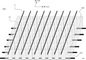
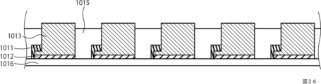
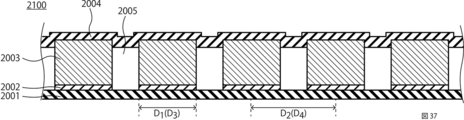
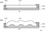
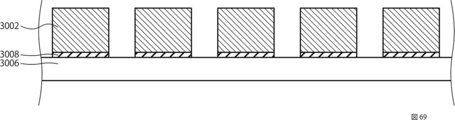
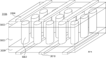
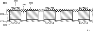
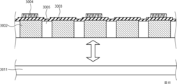
- FIG. 1 is a perspective view of the LED sheet 1100.
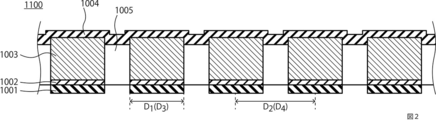
- FIG. 2 shows a cross-sectional view of the LED sheet 1100.
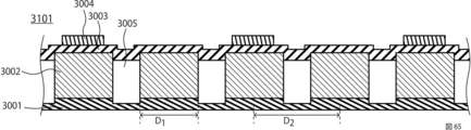
- the LED sheet 1100 includes a plurality of light emitting elements in which a first wiring 1001, a first buffer layer 1002, a light emitting layer 1003 including a diode, and a second wiring 1004 are sequentially stacked.
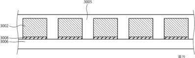
- An insulating layer 1005 is disposed.
- the first wiring 1001 extends in the first direction
- the second wiring 1004 extends in the second direction.
- the light emitting elements are uniformly arranged in the first direction and the second direction with the same size, but the size and arrangement of the light emitting elements are limited to the form shown in FIGS. It is not a thing.
- the LED sheet is used as a display device, it is preferable that the light emitting elements are arranged with a specific shape and pattern.
- the LED sheet 1100 can be used not only for a display device but also for a lighting device.
- the LED sheet 1100 has a first surface and a second surface opposite to the first surface, a plurality of light emitting elements having a light emitting layer 1003 including a diode, and an insulating layer 1005 disposed between the plurality of light emitting elements.
- the first wiring 1001 provided on the first surface side of the light emitting layer 1003 of the plurality of light emitting elements, and the second wiring 1004 provided on the second surface side of the light emitting layer 1003 of the plurality of light emitting elements.
- the LED sheet 1100 has a structure in which a light emitting element is disposed in an insulating layer 1005.
- the LED sheet can be made flexible. Flexible means that the LED sheet 1100 is not broken, chipped, or damaged by repeated winding and opening slowly 10 times on a cylindrical bar having a diameter of 200 mm under an atmospheric pressure environment of 25 ° C. Say.
- the LED sheet 1100 does not include a single crystal epitaxial growth substrate for growing the light emitting layer 1003 and is not used in manufacturing, the LED sheet 1100 can be manufactured at low cost.
- the LED sheet 1100 can be a passive matrix type that does not include a driving element (switching element) inside. Further, the LED sheet 1100 can be an active matrix type including a driving element therein.
- the switching element is not particularly limited, such as one or more selected from the group consisting of inorganic TFT (Thin Film Transistor) such as Si and IGZO, organic TFT, CMOS and diode.
- the active matrix LED sheet 1100 is also flexible. 1 and 2 show a passive matrix type LED sheet.
- the size of the LED sheet varies from several tens of mm 2 to more than 1 m 2 .
- the first wiring 1001 is a conductor that is in direct contact with the first buffer layer 1002.
- the first wiring 1001 is an electrode of each light emitting element.
- the first wiring 1001 serves as one of the anode and the cathode of the light emitting layer 1003.
- the first wiring 1001 is in direct contact with the first buffer layer 1002.
- the surface of the first buffer layer 1002 that is in contact with the first wiring 1001 is opposite to the surface of the first buffer layer 1002 that faces the second wiring 1004. It is preferable that the plurality of light emitting elements included in the LED sheet 1100 are electrically connected via the first wiring 1001.
- the first wiring 1001 includes either a metal film or a transparent conductive film.
- the first wiring 1001 can be a transparent electrode.
- the first wiring 1001 may be a laminated film.
- a metal film may be used for the first wiring 1001, and the first wiring 1001 may also function as a reflector.
- the first wiring 1001 may be able to electrically connect a plurality of light emitting elements arranged as shown in FIGS.
- the LED sheet 1100 is of an active matrix type
- one of the first wiring 1001 and the second wiring 1004 is connected to a driving element that selects a light emitting element that emits light.
- the LED sheet 1100 is an active matrix type
- one of the first wiring and the second wiring not connected to the driving element is a line-shaped, mesh-shaped, or film-shaped conductor, and a plurality of light-emitting elements Are electrically connected by a line, mesh, or film conductor.
- the first wiring 1001 includes a form that becomes an electrode of a light emitting element, a form that is a wiring connected to a driving element, a form that is an electrode of a driving element, and the like.
- the first buffer layer 1002 contains a layered compound.
- the first buffer layer 1002 is preferably plate-shaped.
- the first buffer layer 1002 is preferably a layer made of a layered compound.
- the first buffer layer 1002 is disposed between the first wiring 1001 and the light emitting layer 1003.
- the surface of the first buffer layer 1002 facing the light emitting layer 1003 is opposite to the surface of the first buffer layer 1002 facing the first wiring 1001.
- the first buffer layer 1002 is a single crystal containing a plurality of two-dimensional sheet-like layered compounds, or the crystal orientation of the surface facing the light emitting layer 1003 of the first buffer layer 1002 is uniform (the crystal orientation of the layered compound). is there.
- the crystallinity of the first buffer layer 1002 is determined by four-axis X-ray diffraction measurement or transmission electron microscope observation.
- a two-dimensional layered material such as graphene, a hexagonal metal such as hafnium or an alloy, or a ceramic may be used.
- the layered compound is a two-dimensional sheet extending in the surface direction of the first buffer layer 1002.
- a metal chalcogenide is preferable.
- graphene is also a layered compound, graphene cannot change the lattice constant according to the light emitting layer 1003.
- the lattice constant of the layered compound can be controlled by selecting the metal and the chalcogen element and the ratio thereof.
- a metal chalcogenide represented by MSe ⁇ S ⁇ Te ⁇ O ⁇ is preferable.
- M which is a metal contained in the metal chalcogenide is Ti, Zr, Hf, V, Nb, Ta, Cr, Mo, W, Zn, Cd, Ga, In, Ge, Sn, Pt, Au, Cu, Ag, Mn , Fe, Co, Ni, Pb, and Bi.
- ⁇ , ⁇ and ⁇ are 0.0 ⁇ ⁇ ⁇ 2.0, 0.0 ⁇ ⁇ ⁇ 2.0, 0.0 ⁇ ⁇ ⁇ 2.0, 0.0 ⁇ ⁇ ⁇ 2.0 and 1.0. It is preferable that ⁇ ⁇ + ⁇ + ⁇ + ⁇ ⁇ 2.0 is satisfied.
- ⁇ , ⁇ and ⁇ are 0.0 ⁇ ⁇ ⁇ 2.0, 0.0 ⁇ ⁇ ⁇ 2.0, 0.0 ⁇ ⁇ ⁇ 2.0, 0.0 ⁇ ⁇ ⁇ 2.0, 0 0.0 ⁇ + ⁇ + ⁇ and 1.0 ⁇ ⁇ + ⁇ + ⁇ + ⁇ ⁇ 2.0 are preferably satisfied.
- M which is a metal contained in the metal chalcogenide, preferably contains at least one selected from the group consisting of Mo, W, and Cr. The selection and ratio of metal chalcogenide elements are changed according to the light emitting layer 1003 to be epitaxially grown.
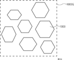
- the diameter (D1) of the first buffer layer 1002 is preferably in the range of 0.1 ⁇ m to 200 ⁇ m. Within this range, the light source is suitable for a display device.
- the diameter of the first buffer layer 1002 is determined as an inscribed circle diameter and a circumscribed circle diameter of each first buffer layer 1002 in a cross section perpendicular to the stacking direction of the light emitting elements. The average value of the determined inscribed circle diameter and circumscribed circle diameter is defined as the diameter of each first buffer layer.
- the diameter of the columnar body in which the first buffer layer 1002 and the light emitting layer 1003 are stacked depends on the diameter of the first buffer layer 1002.
- the diameter of the first buffer layer 1002 (columnar material) is preferably 1 ⁇ m or more and 200 ⁇ m or less. It is preferable that the cross-sectional area and the diameter of the first buffer layer 1002 are changed according to required luminance or the like.
- the plate shape (cross-sectional shape) of the first buffer layer 1002 is often a polygonal column shape such as a disc shape, a triangular column shape, or a hexagonal column shape, but may be any plate shape.
- the shapes of the adjacent first buffer layers 1002 may be different.
- the shortest distance (D2) between the centers of the first buffer layers 1002 (columnar objects) of the plurality of light emitting elements is 0.5 ⁇ m or more and 500 ⁇ m or less.
- a plurality of light emitting elements are included in the LED sheet 10. The plurality of light emitting elements are separated from each other, and there is a gap between the plurality of light emitting elements.
- the shortest distance between the centers of the first buffer layers 1002 of the plurality of light emitting elements is obtained as follows. First, the center point of the first buffer layer 1002 of one light emitting element and the center point of the first buffer layer 1002 of a plurality of light emitting elements around it are obtained.
- the shortest distance between the center point of the first buffer layer 1002 of one light emitting element and the center point of the first buffer layer 1002 of the plurality of light emitting elements on the outer periphery of the light emitting element is the distance between the plurality of light emitting elements.
- the shortest distance between the centers of the first buffer layers 1002 is used.
- the center point of the first buffer layer 1002 of the light emitting element is the center of the circumscribed circle of the first buffer layer 1002.
- the shortest distance between the centers of the first buffer layers 1002 (columnar objects) of the plurality of light emitting elements is more preferably 5 ⁇ m to 300 ⁇ m, and more preferably 30 ⁇ m to 100 ⁇ m.
- the number of pixels of the shortest distance product between the centers of the first buffer layers 1002 of the plurality of light emitting elements is changed.
- the thickness of the first buffer layer 1002 is not particularly limited.
- the thickness of the first buffer layer 1002 is, for example, not less than 10 nm and not more than 1000 nm.
- the variation in the thickness of the first buffer layer 1002 is preferably as small as possible.
- the first buffer layer 1002 and the light emitting layer 1003 are in a heteroepitaxial relationship.
- the stacking direction of the light emitting elements is parallel to the hexagonal c-axis of the metal chalcogenide.
- the metal chalcogenide perpendicular to the stacking direction of the light emitting elements is parallel to the hexagonal a and b axes.
- the orientation of the metal chalcogenide parallel to the substrate surface is random and is not particularly limited as viewed perpendicularly from the substrate surface.
- the metal chalcogenide can arbitrarily change the lattice constant by selecting the element, the lattice constant of the single crystal layer to be epitaxially grown and the lattice constant of the metal chalcogenide can be matched by changing the composition of the metal chalcogenide. That is, by changing the composition of the metal chalcogenide according to the single crystal layer to be epitaxially grown and the crystal orientation to be grown, for example, a substrate suitable for epitaxial growth such as GaN, InN, and AlN can be prepared. In these hexagonal nitrides, the plane orientation for growth is the 0001 direction.
- the difference between the in-plane lattice constant of the first buffer layer 1002 and the in-plane lattice constant of the layer that is closest to the first buffer layer 1002 among the light emitting layers 1003 in which a plurality of layers are stacked ([[the first buffer layer 1002 of In-plane lattice constant]-[in-plane lattice constant of the light emitting layer 1003 closest to the first buffer layer 1002] / [in-plane lattice constant of the first buffer layer 1002]) within ⁇ 1%
- the difference in lattice constant is large, epitaxial growth is difficult, and if the deviation is large, epitaxial growth does not occur or crystal defects are likely to occur, so that the in-plane lattice constant of the first buffer layer 1002 and a plurality of layers are easily formed.
- the difference in the in-plane lattice constant of the layer present on the first buffer layer 1002 side of the light emitting layer 1003 in which is stacked is within ⁇ 0.5%.
- the child constant is obtained by four-axis X-ray diffraction measurement, or is generally determined by the composition ratio of the metal chalcogenide constituting the first buffer layer 1002.
- MoS 1.6 Se 0.4 is used, and the error between the GaN a-axis length 3.189 mm and the metal chalcogenide a-axis length 3.189 mm is 0.0%, which is suitable for epitaxial growth of GaN. It is.
- the two-dimensional sheet-shaped metal chalcogenide that is in direct contact with the light emitting layer 1003 of the first buffer layer 1002 may be composed of a plurality of two-dimensional sheet-shaped metal chalcogenides.
- the surface of the first buffer layer 1002 that is in direct contact with the light emitting layer 1003 is arranged so that the crystal orientations of the plurality of two-dimensional sheet-shaped metal chalcogenides are aligned.
- a plurality of two-dimensional sheet-shaped metal chalcogenides may be overlapped, and there may be a step.
- the surface of the first buffer layer 1002 that is in direct contact with the light emitting layer 1003 is not a metal chalcogenide of a single two-dimensional sheet at the time of peeling from the substrate used at the time of manufacturing, a plurality of two-dimensional sheets of If the crystal orientation of the metal chalcogenide is uniform, the light emitting layer 1003 can be epitaxially grown on the first buffer layer 1002. Since epitaxial growth is possible even if it is not a perfect sheet, a member in which a plurality of first buffer layers 1002 are arranged on a substrate can be manufactured at low cost. And the production cost of an LED sheet can be suppressed by producing an LED sheet using the board
- the light emitting layer 1003 is a light emitting diode disposed between the first buffer layer 1002 and the second wiring 1004.
- the light emitting layer 1003 is in direct contact with the first buffer layer 1002 and in direct contact with the second wiring 1004.
- the surface in which the light emitting layer 1003 is in direct contact with the second wiring 1004 is opposite to the surface in direct contact with the first buffer layer 1002.
- the light emitting layer 1003 includes a first conductivity type semiconductor layer (compound semiconductor layer), an active layer, and a second conductivity type semiconductor layer (compound semiconductor layer).
- the light emitting layer 1003 includes a hexagonal nitride semiconductor layer.
- the light-emitting layer 1003 is preferably formed by stacking a plurality of hexagonal nitride semiconductor layers.
- the plurality of layers of the light emitting layer 1003 are preferably in a heteroepitaxial relationship. That is, a quantum well structure that improves the luminous efficiency is included.
- the nitride semiconductor layer is preferably a single crystal layer of GaN, InN, AlN, and two or more mixed compositions selected from the group consisting of GaN, InN, and AlN.
- the in-plane lattice constant of the nitride semiconductor layer has a width from 3.111 to 3.532.
- the metal chalcogenide composition ratio may be slightly changed in consideration of the difference in thermal expansion coefficient during film formation and the growth rate.
- Compound semiconductors (including active layers) used for the light emitting layer 1003 include GaN, InN, AlN, and two or more mixed compositions selected from the group consisting of GaN, InN, and AlN, as well as GaAs.
- Examples include arsenic compound semiconductors and phosphorus compound semiconductors such as InGaAlP.
- the arsenic compound semiconductor and the phosphorus compound semiconductor can have the same in-plane lattice constant with the first buffer layer 1002 as in the case of the nitride semiconductor.
- An arsenic compound semiconductor or a phosphorus compound semiconductor can be preferably grown as the light emitting layer 1003 from the first buffer layer 1002. That is, the first conductivity type semiconductor layer, the active layer, and the second conductivity type semiconductor layer are semiconductor layers including at least one selected from the group consisting of nitride semiconductors, arsenic compound semiconductors, and phosphorus compound semiconductors. .
- the light emitting layer 1003 When the light emitting layer 1003 is a blue light emitting diode, the light emitting layer 1003 includes, for example, a first conductivity type GaN, a first conductivity type AlGaN, an InGaN, a second conductivity type AlGaN, and a second conductivity type GaN.
- the in-plane lattice constant of the first buffer layer 1002 is set to GaN.
- MoS 1.6 Se 0.4 for the metal chalcogenide, the lattice constants of the metal chalcogenide and GaN are matched.
- the diameter (D3) of the light emitting layer 1003 is preferably in the range of 0.1 ⁇ m or more and 200 ⁇ m or less. Within this range, the light source is suitable for a display device. Regarding the diameter of the light emitting layer 1003, the inscribed circle diameter and the circumscribed circle diameter of the light emitting layer 1003 are obtained in a cross section perpendicular to the stacking direction of the light emitting elements. The average value of the obtained inscribed circle diameter and circumscribed circle diameter is defined as the diameter of each light emitting layer 1003.
- the diameter of the columnar body in which the first buffer layer 1002 and the light emitting layer 1003 are stacked is affected by the diameter of the first buffer layer 1002.
- the diameter of the light emitting layer 1003 (columnar material) is preferably 1 ⁇ m or more and 200 ⁇ m or less.
- the cross-sectional area and diameter of the light emitting layer 1003 are preferably changed according to required luminance or the like.
- the cross-sectional shape of the light emitting layer 1003 is often a polygonal prism shape such as a disc shape, a triangular prism shape, or a hexagonal prism shape, but is not particularly limited.
- the shapes of the adjacent light emitting layers 1003 may be different.
- the shortest distance (D4) between the centers of the light emitting layers 1003 of the plurality of light emitting elements is 0.5 ⁇ m or more and 500 ⁇ m or less.
- a plurality of light emitting elements are included in the LED sheet 1100. The plurality of light emitting elements are separated from each other, and there is a gap between the plurality of light emitting elements.
- the shortest distance between the centers of the light emitting layers 1003 of the plurality of light emitting elements is obtained as follows. First, the center point of the light emitting layer 1003 of one light emitting element and the center point of the light emitting layer 1003 of a plurality of light emitting elements around it are obtained.
- the shortest distance between the center point of the light emitting layer 1003 of one light emitting element and the center point of the light emitting layer 1003 of the plurality of light emitting elements on the outer periphery of the light emitting element is the light emitting layer 1003 of the plurality of light emitting elements.
- the center point of the light emitting layer 1003 of the light emitting element is the center of the circumscribed circle of the light emitting layer 1003.
- the shortest distance between the centers of the light emitting layers 1003 of the plurality of light emitting elements is more preferably 5 ⁇ m to 300 ⁇ m, and 30 ⁇ m to 100 ⁇ m.
- the number of pixels of the shortest distance product between the centers of the light emitting layers 1003 of the plurality of light emitting elements is changed.
- the second wiring 1004 is a conductor that is in direct contact with the light emitting layer 1003.
- the second wiring 2 is an electrode of each light emitting element. It is preferable that the plurality of light emitting elements included in the LED sheet 1100 are electrically connected via the second wiring 1004.
- the second wiring 1004 includes either a metal film or a transparent conductive film.
- the second wiring 1004 can be a transparent electrode.
- the second wiring 1004 may be a laminated film.
- a metal film may be used for the second wiring 1004, and the second wiring 1004 may also function as a reflector.
- the second wiring 1004 includes a form that becomes an electrode of a light emitting element, a form that is a wiring connected to the driving element, a form that is an electrode of the driving element, and the like.
- the insulating layer 1005 is disposed between the plurality of light emitting elements.
- the insulating layer 1005 preferably holds the light emitting element and becomes a base of the LED sheet 1100.
- the insulating layer 1005 is made of an insulating material containing a polymer.
- the surface of the insulating layer 1005 facing the light emitting element is in direct contact with at least part of the surface of the light emitting element facing the insulating layer 1005 (side surface of the light emitting element).
- the surface of the insulating layer 1005 facing the light emitting element includes a direction perpendicular to the stacking direction of the light emitting elements.
- the insulating layer 1005 is in direct contact with the first buffer layer 1002, the light emitting layer 1003, or the side surfaces of the first buffer layer 1002 and the light emitting layer 1003.
- the insulating layer 1005 is filled between the light emitting layers 1003 grown in a columnar shape and spreads in a sheet shape.
- the insulating layer 1005 is a polymer spacer.
- the thickness of the insulating layer 1005 is such that it covers the first buffer layer 1002 and the light emitting layer 1003 grown thereon.
- the insulating layer having a thickness of about 2 to 5 ⁇ m insulates the light emitting layer, It is a part that bears the flexibility of the light-emitting element sheet and the display sheet as products, and it is preferable to select a material based on strength and workability.
- a colored or colorless polymer can be used as the insulating layer 1005. From the viewpoint of reducing light absorption loss, a colorless and transparent one is more desirable.
- the polymer that can be used as the insulating layer 1005 include a fluororesin, an epoxy resin, and a silicon resin.
- the insulating layer 1005 is filled with, for example, a fluorine resin, a transparent resin, a transparent polymer, or the like at least between a plurality of light emitting layers including a diode. Specifically, at least a part of the side surface of the light emitting layer 1003 is covered, and at least filled between the plurality of light emitting layers so that the plurality of light emitting layers 1003 do not directly contact each other. More specifically, in the case where the first wiring 1001 and the second wiring 1004 are also formed on part of the side surface of the light emitting layer 1003, the insulating layer 1005 is also formed on the outer peripheral side surface of the first wiring 1001 and the second wiring 1004. May be formed.
- an insulating layer 1005 is formed on the surface where the light emitting layer 1003 which is the upper end surface of the light emitting layer 1003 is in contact with the first wiring 1001 and the surface where the light emitting layer 1003 which is the lower end surface is in contact with the second wiring 1004.
- the insulating layer 1005 may cover a part of the side surfaces of the first wiring 1001 and the second wiring 1004, but the surface opposite to the surface facing the light emitting layer 1003 of the first wiring 1001.
- the insulating layer 1005 is preferably not formed on the surface of the second wiring 1004 opposite to the surface facing the light emitting layer 1003.
- the insulating layer 1005 is in contact with the light emitting layer 1003.
- the light emitted from the light emitting layer 1003 is totally reflected on the surface in contact with the insulating layer 1005, color mixture of pixels can be prevented.
- the light emitting elements 1003 are densely arranged, the interval between the light emitting elements is narrowed and the color mixture between the pixels is likely to occur.
- the material which increases the refractive index difference between the light emitting layer 1003 and the insulating layer 1005 is insulated. By selecting the layer 1005, color mixture between pixels can be prevented.
- the refractive index n 3 of the light emitting layer 1003 is approximately 3.0, specifically 2.4 to 2.5, and the same numerical values as other nitride semiconductor layers, The details are close to 1.9 to 2.9.
- the refractive index of the light-emitting layer 1003 is around 2.4 to 2.5, it is preferable to select a material for the insulating layer 1005 that is smaller than the refractive index n 3 of the light-emitting layer 3.
- the refractive index n 5 of the insulating layer 1005 is less than 2.5, preferably less than 1.9, more preferably less than 1.5.
- the refractive index difference between the insulating layer 1005 and the light emitting layer 1003 is very large, preventing color mixture between pixels, and further the light emission intensity of the LED sheet 1100. It is very preferable in that it becomes high.
- the light emission 1002 is epitaxially grown on the first buffer layer 1002.
- a light emitting layer 1003 in which an n-type GaN layer, a superlattice (Strained-Layer ⁇ Superlattice; SLS), a multi-quantum well (MQW) as an active layer, and a p-type GaN layer are stacked will be described as an example.
- SLS relaxed-Layer ⁇ Superlattice
- MQW multi-quantum well
- n-type GaN is grown on the first buffer layer 1002.
- the growth of the n-type GaN layer is preferably performed by supplying a nitrogen gas as a carrier gas, in which the first buffer layer 1002 is not easily destroyed.
- a nitrogen gas as a carrier gas
- the n-type impurity one or more selected from the group consisting of Si, Ge, Te and Sn is used.
- the size and shape of the ground plane with the n-type GaN first buffer layer 1002 are controlled by the shape of the first buffer layer 1002.
- the height of the n-type GaN layer is typically about several ⁇ m, and is controlled to be the designed height.
- the first buffer layer 1002 is selected so that the (0001) plane of the n-type GaN layer grows.
- the n-type GaN layer may be further grown using a mixed gas of nitrogen gas and hydrogen gas or hydrogen gas as a carrier gas from the viewpoint of growth control and the like.
- a mixed gas of nitrogen gas and hydrogen gas or hydrogen gas as a carrier gas from the viewpoint of growth control and the like.
- the (0001) plane which is a polar plane, but also a semipolar plane such as the (10-11) plane and a non-polar plane such as the (1-100) plane Polar faces may be mixed.
- the internal electric field due to polarization may be reduced and the droop phenomenon may be suppressed.
- the n-type GaN layer on the superlattice or multiple quantum well side may be thicker than the first buffer layer 1002. Note that the emission spectrum can be controlled by the cross-sectional diameter of the light-emitting layer 1003.
- a stacked structure in which, for example, a plurality of 2 nm n-type GaN and 1 nm InGaN (In ⁇ Ga) are periodically stacked as superlattices is formed on the nGaN layer.
- the superlattice may be omitted.
- Multiple quantum wells are formed on the superlattice or n-type GaN layer.
- the multiple quantum well has a structure in which a plurality of barrier layers (non-doped GaN) layers and well layers (InGaN) layers are stacked.
- An example of the stack of multiple quantum wells is a structure in which 10 or less pairs of InGaN and GaN are stacked (for example, 8 pairs in the case of blue light emission).
- the thickness of each layer of the multiple quantum well is several nm.
- the emission spectrum can be controlled by changing the composition of In or Al in the well layer.
- a p-type GaN layer is grown on the multiple quantum well.
- the p-type impurity one or more selected from the group consisting of Mg and Zn is used.
- the p-type GaN layer has a single layer structure or a laminated structure.
- the thickness of the p-type GaN layer is, for example, about 150 nm.
- On the surface of the p-type GaN layer not only the (0001) plane but also a semipolar plane such as the (10-11) plane as with the surface of the n-type GaN layer And nonpolar surfaces such as (1-100) surfaces may be mixed.
- the thickness of the p-type GaN layer can be controlled in the same manner as the n-type GaN layer.
- the n-type GaN of the light emitting layer 1003 manufactured by such a method is in contact with the first wiring 1001 and the p-type GaN is in contact with the second wiring 1004.
- the diameter of the light emitting layer 1003 (the diameter of the inscribed circle of the columnar object) can be changed. At this time, the diameter of the light emitting layer 1003 on the first wiring 1001 side is different from the diameter on the second wiring side 1004 side.
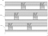
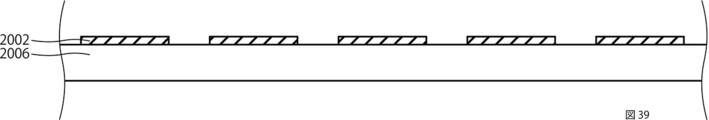
- the method for producing the LED sheet 1100 described below includes a step (first step) of forming a plurality of first buffer layer precursors in a plate shape (dot shape) on a non-oriented substrate, and a first buffer layer precursor.
- Heating a member formed on the non-oriented substrate to form a plurality of first buffer layers containing the layered compound on the non-oriented substrate (second step), and a plurality of first A step of forming a plurality of pillars by epitaxially growing a light emitting layer on the buffer layer (third step), a step of forming an insulating layer filling between the plurality of pillars (fourth step), and a plurality of pillars; A step of forming a second wiring on a surface of the light emitting layer opposite to the surface facing the first buffer layer (fifth step), a non-oriented substrate is peeled off, and a plurality of columnar objects are formed.
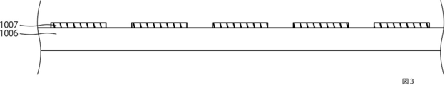
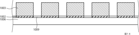
- FIG. 3 shows a step (first step) of forming a plurality of first buffer layer precursors 1007 on the non-oriented substrate 1006 in a plate shape.
- the non-oriented substrate 1006 may be anything as long as there is no crystal orientation that is uniquely determined over the entire surface of the substrate, such as glass, metal, polycrystal, plastic (resin), ceramics, and amorphous.
- the non-oriented substrate 1006 is not particularly limited as long as it holds the first buffer layer 1002 necessary for epitaxial growth. It is not necessary to use an expensive single crystal base material for the non-oriented substrate 1006. Further, the non-oriented substrate 1006 is not included in the light emitting element.
- the first buffer layer precursor 1007 is obtained by forming a metal contained in a layered compound into a plate shape.
- the first buffer layer precursor 1007 that is a metal (or alloy) is formed in a plate shape by forming and patterning a metal film (or alloy film).
- the first buffer layer precursor 1007 includes Ti, Zr, Hf, V, Nb, Ta, Cr, Mo, W, Zn, Cd, Ga, In, Ge, Sn, Pt, Au, Cu, Ag, Mn, and Fe.
- the metal of the first buffer layer precursor 1007 is selected according to the light emitting layer 1003 to be epitaxially grown.
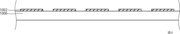
- a member in which the first buffer layer precursor 1007 is formed on the non-oriented substrate 1006 is heated to form a plurality of first buffer layers 1002 including a layered compound on the non-oriented substrate 1006 in a plate shape.
- the process (2nd process) formed in is shown.
- the heating is performed in an atmosphere containing one or more selected from the group consisting of Se, S, Te, and O (oxygen).
- the first buffer layer 1002 is formed on the non-oriented substrate 1006.
- Heating conditions are selected according to the light emitting layer 1003 to be epitaxially grown. It is preferable that all the plate-like first buffer layers 1002 have the same composition.
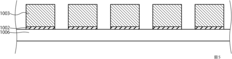
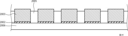
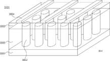
- FIG. 5 shows a step (third step) in which the light emitting layer 1003 is epitaxially grown on the plurality of first buffer layers 1002 to form a plurality of columnar objects.
- the columnar body includes one first buffer layer 1002 and a light emitting layer 1003 formed on the first buffer layer 1002. Since the lattice constant of the first buffer layer 1002 matches the lattice constant of the layer to be epitaxially grown, the light emitting layer 1003 grows epitaxially on the first buffer layer 1002. Since the growth hardly occurs on the non-oriented substrate 1006, the light emitting layer 1003 is selectively grown on the first buffer layer 1002.
- the light emitting layer 1003 includes a plurality of layers such as an electrode contact layer and a quantum well, epitaxial growth is performed a plurality of times, and the light emitting layer 1003 is epitaxially grown on the plurality of first buffer layers 1002 to form a plurality of columnar objects.
- FIG. 6 shows a step (fourth step) of forming an insulating layer 1005 filling between a plurality of columnar objects.
- An insulating layer 1005 is formed so as to fill a space between the columnar members of a member in which a plurality of columnar materials are formed on the non-oriented substrate 1006.
- the insulating layer 1005 can be formed by dipping, spraying, spin coating, or the like.
- the insulating layer 1005 may expose a part of the columnar object on the side opposite to the non-oriented substrate 1006 side, or the columnar object may be completely covered. If necessary, since the light emitting layer 1003 is in direct contact with the second wiring 1004, part of the insulating layer 1005 can be removed to expose at least part of the surface of the light emitting layer 1003.
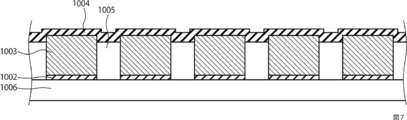
- FIG. 7 shows a step (fifth step) of forming the second wiring 1004 on the surface opposite to the surface facing the plurality of first buffer layers 1002 of the plurality of columnar light emitting layers 1003. This step may be performed after the non-oriented substrate 1006 is peeled off.
- a conductive second wiring 1004 is formed over the light emitting layer 1003. This wiring may be a wiring that connects the light emitting elements arranged side by side, or may be a wiring that is connected to a driving element. In FIG. 7, the second wiring 1004 is formed so as to connect the light emitting elements arranged in the horizontal direction.
- FIG. 8 shows a step of peeling the non-oriented substrate 1006. Then, by forming the first wiring 1001 so as to be in direct contact with the lower side of the first buffer layer 1002 (the surface opposite to the surface facing the light emitting layer 1003 of the first buffer layer 1002), FIG. The LED sheet 1100 shown in the cross-sectional view is obtained.
- This wiring may be a wiring connecting the light emitting elements arranged side by side or a wiring connecting to the driving element.
- the second wiring 1004 is formed so as to connect the light emitting elements arranged in the depth direction of FIG.
- the second wiring 1004 side is preferably fixed to a base material (not shown) and peeled off. Since the first buffer layer 1002 is fixed to the non-oriented substrate 1006 by van der Waals contact, the first buffer layer 1002 is physically easily peeled off. By peeling off the insulating layer 1005, the light emitting element portion including the light emitting layer 1003 epitaxially grown with the first buffer layer 1002 is attached to the sheet side of the insulating layer 1005. At this time, a part of the layered compound may be peeled off. The first buffer layer 1002 remaining on the sheet side may be intentionally peeled off by electrostatic adsorption, ultrasonic treatment, cleaning, etching, or the like.
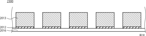
- the LED sheet 1100 can be manufactured without using a very expensive single crystal substrate, the manufacturing cost is lower than when the single crystal substrate is used or manufactured. Significant reduction is achieved. In addition, it is possible to increase the film forming area, which is limited by the wafer shape of the single crystal substrate, and to improve the shape flexibility such as a square shape, which also leads to cost reduction and design flexibility.
- the second embodiment relates to an LED sheet.
- the LED sheet of the second embodiment is a modification of the first embodiment.
- FIG. 9 shows a cross-sectional view of the LED sheet 1101.
- the LED sheet 1101 includes a plurality of light emitting elements in which a first wiring 1001, a first buffer layer 1002, a light emitting layer 1003 including a diode, and a second wiring 1004 are sequentially stacked.
- An insulating layer 1005 is disposed.
- common description is omitted.
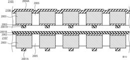
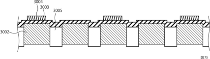
- the difference between the LED sheet 1101 and the LED sheet 1100 is that the insulating layer 1005 is also formed on a part of the surface of the light emitting layer 1003 in contact with the second wiring 1004.
- the second wiring 1004 is in direct contact with the light emitting layer 1003 from between the insulating layers 1005 above the light emitting layer 1003.
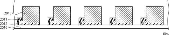
- the third embodiment relates to an LED sheet.
- the LED sheet of the third embodiment is a modification of the first embodiment.
- FIG. 10 shows a cross-sectional view of the LED sheet 1102.
- the LED sheet 1101 includes a plurality of light emitting elements in which a first wiring 1001, a first buffer layer 1002, a light emitting layer 1003 including a diode, and a second wiring 1004 are sequentially stacked.
- An insulating layer 1005 is disposed.
- a common description is omitted.
- the difference between the LED sheet 1101 and the LED sheet 1100 is that the second wiring 1004 side of the light emitting layer 1003 has a conical shape.
- the second wiring 1004 is along the cone shape of the light emitting layer 1003.
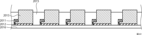
- the fourth embodiment relates to an LED sheet.
- the LED sheet of the fourth embodiment is a modification of the first embodiment.
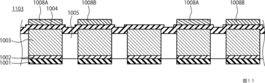
- FIG. 11 shows a cross-sectional view of the LED sheet 1101.
- the LED sheet 1101 includes a plurality of light emitting elements in which a first wiring 1001, a first buffer layer 1002, a light emitting layer 1003 including a diode, and a second wiring 1004 are sequentially stacked.
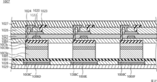
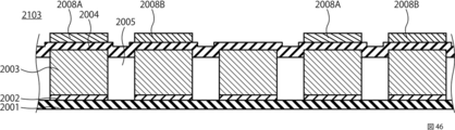
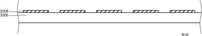
- An insulating layer 1005 is provided, and a transmissive color gamut adjusting layer 1008 is formed over at least part of the light emitting elements.
- a common description is omitted.
- the transmission color gamut adjustment layer 1008 is a phosphor, a color filter, a quantum dot, or a phosphor and a color filter.
- FIG. 11 shows an example of an LED sheet capable of full color display when the light emitting element emits blue light.
- a green phosphor 1008A and a red phosphor 1008B are arranged on the second wiring 1004 for the two light emitting elements, and one light emitting element has a fluorescent light. Neither body nor color filter is placed.
- the emission intensity changes by providing the green phosphor 1008A or the red phosphor 1008B for example, by changing the area of the light emitting element for each color to emit light
- full color display including white can be performed.
- a transmission color gamut adjustment layer 1008 is provided on both sides of the first wiring 1001 and the second wiring 1004.
- a transmission color gamut adjusting layer 1008 is provided on the light emitting surface side.
- the transmission color gamut adjustment layer 1008 is formed by vapor deposition, ink jet, or the like.
- the fifth embodiment relates to an LED sheet.
- the LED sheet of the fifth embodiment is a modification of the first embodiment.
- the LED sheet of the fifth embodiment includes at least a first wiring, a light emitting layer including a diode, a plurality of light emitting elements in which second wirings are sequentially stacked, and an insulating layer arranged between the plurality of light emitting elements.
- the light emitting layer is in direct contact with the first wiring, and the surface of the light emitting layer opposite to the surface in direct contact with the first wiring is in direct contact with the second wiring.
- common description is omitted.
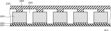
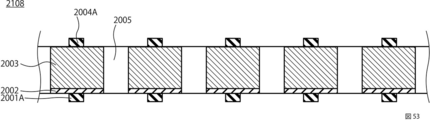
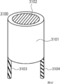
- FIG. 12A shows a cross-sectional view of the LED sheet 1104 of the fifth embodiment.
- the first buffer layer 1002 is not included, and the light emitting layer 1003 is similar to the LED sheet of the first embodiment except that the light emitting layer 1003 is in direct contact with both the first wiring 1001 and the second wiring 1004. Since the first buffer layer 1002 is conductive, it may be included between the light emitting layer 1003 and the first wiring 1001, but the first buffer layer 1002 can be omitted.
- the surface of the light emitting layer 1003 opposite to the surface directly in contact with the first wiring 1001 is in direct contact with the second wiring 1004. Since the first buffer layer 1002 easily absorbs light, it is preferable that the light emission efficiency is improved by removing the layered compound.
- the LED sheet 1104 has a first surface and a second surface opposite to the first surface, and includes a plurality of light emitting elements having a light emitting layer 1003 including a diode, and an insulating layer 1005 disposed between the plurality of light emitting elements.
- a first wiring 1001 provided in contact with the first surface of the light emitting layer 1003 of the plurality of light emitting elements, and a second wiring 1004 provided in contact with the second surface of the light emitting layer 1003 of the plurality of light emitting elements.
- the LED sheet 1104 is produced by a step of forming a plurality of first buffer layer precursors on a non-oriented substrate (seventh step), and the formation of the first buffer layer precursor on the non-oriented substrate.
- Heating the formed member to form a plurality of buffer layers containing a layered compound on a non-oriented substrate in a plate shape (eighth step), and epitaxially growing a light emitting layer on the plurality of first buffer layers A step of forming a plurality of pillars (a ninth step), a step of forming an insulating layer filling between the plurality of pillars (a tenth step), and a surface having a layered compound of the plurality of pillars
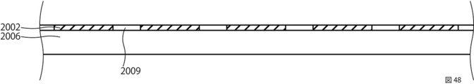
- substrate 1006 and the 1st buffer layer 1002 differs from the preparation methods in 1st Embodiment.
- the method for peeling the first buffer layer 1002 is not limited, but, for example, after the non-oriented substrate 1006 is peeled off, the first buffer layer 1002 may be peeled off by electrostatic adsorption, ultrasonic waves, tape adsorption peeling, etching, washing, or the like.
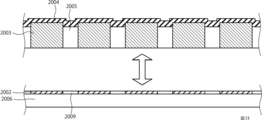
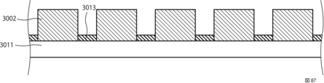
- a method of forming an insulating material, fixing the first buffer layer 1002, and peeling the first buffer layer 1002 together with the insulating material before epitaxial growth will be described with reference to FIGS.
- a step (seventh step) of forming a plurality of first buffer layer precursors in a plate shape on a non-oriented substrate 1006, and a member in which the first buffer layer precursor is formed on the non-oriented substrate are heated.
- a step (eighth step) of forming a plurality of first buffer layers containing a layered compound in a plate shape on a non-oriented substrate is performed.
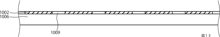
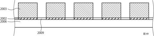
- a resist is formed by the photolithography so that the plate-like first buffer layer 1002 is partially exposed.
- an insulating film 1009 is formed between the first buffer layers 1002 as shown in FIG.
- the insulating film 1009 is formed of, for example, SiO 2 by sputtering.
- the resist is removed by lift-off, and a part of the plate-like first buffer layer 1002 is exposed.
- the first buffer layer 1002 can be removed without using the insulating film 1009.
- the process (9th process) which carries out the epitaxial growth of the light emitting layer 1003 on the some 1st buffer layer 1002, and forms a some columnar thing is performed.
- the step of forming the insulating layer 1005 filling the space between the plurality of pillars (the tenth step) is opposite to the surface of the plurality of pillars 3 having the first buffer layer 1002.
- a step of forming the second wiring on the side surface (11th step) is performed.
- substrate 1006 and the 1st buffer layer 1002 is performed.
- the first buffer layer 1002 fixed by the insulating film 1009 together with the non-oriented substrate 1006 may be peeled off, or may be peeled off separately.
- a step of forming the first wiring 1001 on one surface in a direction perpendicular to the surface of the plurality of columnar objects facing the insulating layer 1005 is performed to obtain the LED sheet 1104 of FIG.
- FIG. 12B shows another LED sheet 1004 ′ that does not include the first buffer layer 1002.
- the diameter of the light emitting layer 1003 on the first wiring 1001 side is thin, and the diameter of the light emitting layer 1003 n on the second wiring 1004 side is large.
- the light emitting layer 1003 is easily caught by the insulating layer 1005 and is difficult to come off between the insulating layers 1005 when being separated from the non-oriented substrate 1006. There is a case.
- the light emitting layer 1003 is provided on the non-oriented substrate 1006 side after peeling, the voids that have escaped from between the insulating layers 1005 become the dots of the LED sheet.
- the diameter of the light emitting layer 1003 is controlled, the adhesion between the light emitting layer 1003 and the insulating layer 1005 is improved, and the non-oriented substrate 1006 is easily peeled. .
- an adhesive may be provided between the light emitting layer 1003 and the insulating layer 1005.
- the adhesive is handled as a material included in the insulating layer 1005.
- the adhesive is not limited as long as the light emitting layer 1003 is difficult to come off from the insulating layer 1005.
- a plurality of means for preventing dot omission of the LED sheet can be combined.
- ⁇ Molecular bonding agent can also be used as an example of an adhesive that prevents missing dots on the LED sheet.
- the molecular bonding agent prevents the light emitting layer 1003 from coming off the insulating layer 1005 by increasing the adhesion between the side surface of the light emitting layer 1003 and the insulating layer 1005.
- a molecular bonding agent is applied to the side surface of the light emitting layer 1003 so as not to adhere to the non-oriented substrate 1006, and then the insulating layer 1005 is formed, and the light emitting layer 1003 and the insulating layer 1005 are bonded.
- a small amount of the insulating layer 1005 is applied to the side surface of the light emitting layer 1003, and then a molecular bonding agent is applied.
- the insulating layer 1005 is further applied to increase the adhesion between the side surface side of the light emitting layer 1003 and the insulating layer 1005. Can be increased.
- adhesion between the non-oriented substrate 1006 and the insulating layer 1005 can be improved.
- the adhesive it is preferable to select a suitable material according to the material to be bonded.
- the insulating film 1009 provided between the insulating layer 1005 and the non-oriented substrate 1006 has low adhesiveness to the non-oriented substrate 1006.
- a material having high adhesiveness can be selected.
- a layer or a film other than the insulating film 1009 may be formed.
- the sixth embodiment relates to an LED sheet.
- the LED sheet of the sixth embodiment is a modification of the first embodiment.
- FIG. 17 shows a cross-sectional view of the LED sheet 1105.
- the LED sheet 1105 includes a plurality of light emitting elements in which a first wiring 1001, a first buffer layer 1002, a light emitting layer 1003 including a diode, and a second wiring 1004 are sequentially stacked.
- An insulating layer 1005 is disposed and includes a driving element 1010 electrically connected to the first wiring 1001. In the first embodiment 1 and the sixth embodiment, common description is omitted.
- a driving element 1010 such as a TFT is formed in an individual light emitting element, and the light emission on / off of the element can be driven by the TFT.
- the light emitting elements can be individually turned on / off by forming the wiring in a stripe shape so that the first wiring 1001 and the second wiring 1004 intersect.
- the seventh embodiment relates to an LED sheet.
- the LED sheet of the seventh embodiment is a modification of the first embodiment.
- FIG. 18 shows a cross-sectional view of the LED sheet 1106.
- the LED sheet 1106 includes a plurality of light emitting elements in which a first wiring 1001, a first buffer layer 1002, a light emitting layer 1003 including a diode, and a second wiring 1004 are sequentially stacked.
- An insulating layer 1005 is disposed and includes a driving element 1010 electrically connected to the second wiring 1004.
- the first embodiment and the sixth embodiment are common except that the drive element 1010 is connected to the second wiring 1004.
- Each of the LED sheets shown in the first to seventh embodiments has a structure that can be manufactured without using a single crystal substrate that is expensive and has limited size and shape, and is a practical LED. It is a sheet. Moreover, these LED sheets are also suitable in that they can be used for display devices and lighting devices in which the light emitting portion can be bent by making them flexible. The LED sheet can be used for displays such as televisions and smartphones. In addition, it can be used for wallpaper, clothing, and flexible displays for bent parts.
- the eighth embodiment is a display device using the LED sheet of the embodiment.
- FIG. 19 shows a conceptual diagram of the display device 1200.
- the display device 1200 includes an LED sheet 1201, a control unit 1202, a power supply unit 1203, and a signal input unit 1204.
- Display device 1200 may be housed in one housing or may be divided into a plurality of housings.
- the LED sheet 1201 is preferably not weathered, but is sealed with a polymer material, a resin material, a glass material, or the like, and has weather resistance.
- the LED sheet 1201 may not be accommodated in the housing as long as the LED sheet 1201 includes a light emitting element control terminal.
- the LED sheet 1201, the control unit 1202, the power supply unit 1203, and the signal input unit 1204 constituting the display device 1200 are connected by wire, wireless, or wired and wireless.
- the LED sheet 1201 controls light emission, non-light emission, light emission intensity, and the like of a specific light emitting element by a signal and power from the control unit 1202.
- the control unit 1202 may process an image signal to be displayed on the LED sheet 1201.
- the signal input to the signal input unit 1204 is processed by the control unit 1202.
- the signal input unit 1204 can have a function of processing an external signal and a communication function such as a tuner.
- the control unit 1202 may be connected to one part of the LED sheet 1201 or may be connected to a plurality of LED sheets 1201.
- the power supply unit 1203 is connected to the control unit 1202 and the signal input unit 1204, and converts the power into power necessary for operating the display device 1200.
- the power supply unit 1203 includes, for example, an AC-DC converter and a DC-DC converter.
- a non-flexible LED sheet with a support that is held on the support by a process of holding on the support can be used.
- the ninth embodiment relates to an LED sheet.
- the LED sheet of the ninth embodiment includes a non-oriented substrate, a first wiring, a second buffer layer, a light emitting layer, a second wiring, and an insulating layer.
- the light emitting layer is disposed between the second buffer layer and the second wiring.
- FIG. 20 shows a cross-sectional view of the LED sheet 1300 of the ninth embodiment.
- An LED sheet 1300 illustrated in FIG. 20 includes a non-oriented substrate 1016 and a plurality of light-emitting elements on the non-oriented substrate 1016, and an insulating layer is disposed between the plurality of light-emitting elements.
- the light emitting layer includes a plurality of layers.
- the light emitting layer 1013 has an extending surface on the second buffer layer 1012 side, and the extending surface is in direct contact with the first wiring 1011. In addition, the extending surface is disposed between the first wiring 1011 and the second buffer layer 1012.
- the light emitting element of the LED sheet 1300 has a horizontal device structure.
- the layer disposed closest to the second buffer layer 1012 of the light emitting layer 1013 includes a surface that is not stacked with other layers of the light emitting layer 1013.
- This non-stacked surface is a surface facing the side opposite to the surface facing the second buffer layer 1012 of the light emitting layer 1013.
- This non-stacked surface is directly connected to the first wiring 1011.
- a layer disposed on the opposite side of the light emitting layer 1013 with respect to the second buffer layer 1012 and the second wiring 1014 are directly connected.
- the first wiring 1011 and the second wiring 1014 are in direct contact with the surface of the light emitting layer 1013 facing away from the surface facing the second buffer layer 1012.
- the second buffer layer 1012 is a plate-like crystal and is a hexagonal metal alloy made of two or more kinds of metals.
- the second buffer layer 1012 is preferably a layer made of a hexagonal metal alloy made of two or more kinds of metals.
- the second buffer layer 1012 is disposed between the non-oriented substrate 1016 and the light emitting layer 1013.
- the surface of the second buffer layer 1012 facing the light emitting layer 1013 is opposite to the surface of the second buffer layer 1012 facing the non-oriented substrate 1016.
- the crystal orientation of the surface of the second buffer layer 1012 facing the light emitting layer 1003 is uniform or the second buffer layer 1012 is a single crystal.
- the crystallinity of the second buffer layer 1012 is determined by four-axis X-ray diffraction measurement or transmission electron microscope observation.
- the buffer layer may be in direct contact with the first electrode 1.
- composition of the second buffer layer 1012 is as follows.
- Hexagonal metal alloys include, for example, Mg, Ca, Sc, Ti, Fe, Co, Ni, Zn, Sr, Y, Zr, Tc, Ru, Cd, In, Sn, Sb, Ba, Hf, Re, Os and An alloy containing one or more metals selected from the group consisting of Pb. Since the lattice constant of the metal alloy can be arbitrarily changed by selecting an element, the lattice constant of the light emitting layer 1013 to be epitaxially grown can be matched with the lattice constant of the metal alloy by changing the composition of the metal alloy.
- a base material suitable for epitaxial growth such as GaN, InN, and AlN can be prepared.
- the plane orientation for growth is the 0001 direction.
- a hexagonal metal alloy formed by alloying with a hexagonal metal may be included.
- Hexagonal metal alloys include, for example, Mg, Ca, Sc, Ti, Fe, Co, Ni, Zn, Sr, Y, Zr, Tc, Ru, Cd, In, Sn, Sb, Ba, Hf, Re, Os and An alloy made of two or more metals selected from the group consisting of Pb is preferable.
- the hexagonal metal alloy is preferably an alloy containing one or more metals selected from the group consisting of Cr, Mo and W.
- the diameter (D5) of the second buffer layer 1012 is in the range of 0.1 ⁇ m to 200 ⁇ m. Within this range, the light source is suitable for a display device.
- the diameter of the second buffer layer 1012 the inscribed circle diameter and circumscribed circle diameter of each second buffer layer 1012 are obtained in a cross section perpendicular to the stacking direction of the light emitting elements.
- the average value of the obtained inscribed circle diameter and circumscribed circle diameter is set as the diameter of each second buffer layer 1012.
- the diameter of the columnar body in which the second buffer layer 1012 and the light emitting layer 1013 are stacked depends on the diameter of the first buffer layer 1002.
- the diameter of the second buffer layer 1012 (columnar material) is preferably 1 ⁇ m or more and 200 ⁇ m or less.
- the cross-sectional area and diameter of the second buffer layer 1012 are preferably changed according to required luminance or the like.
- the plate shape (cross-sectional shape) of the second buffer layer 1012 is often a polygonal column shape such as a disc shape, a triangular column shape, or a hexagonal column shape, but may be any plate shape.
- the shapes of the adjacent hexagonal compound layers 2 may be different.
- the shortest distance (D6) between the centers of the second buffer layers 1012 (columnar objects) of the plurality of light emitting elements is 0.5 ⁇ m or more and 500 ⁇ m or less.
- a plurality of light emitting elements are included in the LED sheet 10. The plurality of light emitting elements are separated from each other, and there is a gap between the plurality of light emitting elements.
- the shortest distance between the centers of the second buffer layers 1012 of the plurality of light emitting elements is obtained as follows. First, the center point of the second buffer layer 1012 of one light emitting element and the center point of the second buffer layer 1012 of a plurality of light emitting elements around it are obtained.
- the shortest distance between the center point of the second buffer layer 1012 of one light emitting element and the center point of the second buffer layer 1012 of the plurality of light emitting elements on the outer periphery of the light emitting element is the distance between the plurality of light emitting elements.
- the shortest distance between the centers of the second buffer layers 1012 is used.
- the center point of the second buffer layer 1012 of the light emitting element is the center of the circumscribed circle of the first buffer layer 1002.
- the shortest distance between the centers of the second buffer layers 1012 (columnar objects) of the plurality of light emitting elements is more preferably 5 ⁇ m to 300 ⁇ m, and 30 ⁇ m to 100 ⁇ m. It is changed according to the number of pixels of the shortest distance product between the centers of the second buffer layers 1012 of the plurality of light emitting elements.
- the thickness of the second buffer layer 1012 is not particularly limited.
- the thickness of the second buffer layer 1012 is, for example, not less than 10 nm and not more than 1000 nm. A smaller variation in the thickness of the second buffer layer 1012 is better.
- the second buffer layer 1012 and the light emitting layer 1013 are heteroepitaxial.
- the stacking direction of the light emitting elements is parallel to the hexagonal c-axis of the hexagonal metal alloy.
- the hexagonal metal alloy perpendicular to the stacking direction of the light emitting elements is parallel to the hexagonal a and b axes.
- the orientation of the second buffer layer 1012 is random and not particularly limited.
- the difference between the in-plane lattice constant of the second buffer layer 1012 and the in-plane lattice constant of the layer that is closest to the second buffer layer 1012 among the light emitting layers 1013 in which a plurality of layers are stacked ([the second buffer layer 1012 In-plane lattice constant]-[in-plane lattice constant of the light emitting layer 1013 closest to the second buffer layer 1012] / [in-plane lattice constant of the second buffer layer 1012]) is within ⁇ 1% If the difference between the lattice constants is large, epitaxial growth is difficult, and if the deviation is large, epitaxial growth does not occur.
- the difference in the in-plane lattice constant of the layer existing closest to the second buffer layer 1012 is more preferably within ⁇ 0.5%.
- it is generally determined by the composition ratio of the metal alloy constituting the second buffer layer 1012.
- Hf 0.95 is included in the metal alloy.
- -Ti 0.05 series alloy is used, and the error between the GaN a-axis length 3.189 mm and the metal alloy a-axis length 3.189 mm is 0.0%, which is suitable for epitaxial growth of GaN.
- the composition ratio of the second buffer layer 1012 may be slightly changed in consideration of the difference in thermal expansion coefficient and the growth rate.
- the plate-shaped hexagonal metal alloy has a case where the crystal system on the non-oriented substrate 1016 side is not a hexagonal crystal system or has a large mismatch with an epitaxial growth layer having an intended composition. It is important that the surface opposite to the non-oriented substrate 1016 side of 1012 is composed of a hexagonal metal alloy. Further, there are cases where the plate-like surface includes a step or a grain boundary, but there is no problem if high-quality epitaxial growth is possible. Since the second buffer layer 1012 can be epitaxially grown even if it is not a perfect single crystal, the LED sheet 1300 is provided at low cost.
- the method for producing the LED sheet 1300 described below includes a step of forming a plurality of second buffer layer precursors in a plate shape (dot shape) on a non-oriented substrate (14th step), and a second buffer layer precursor.
- Annealing a member formed on the non-oriented substrate to form a plurality of second buffer layers in a plate shape on the non-oriented substrate (15th step), and on the plurality of second buffer layers A step of epitaxially growing the light emitting layer to form a plurality of pillars (step 16), a step of removing a part of the light emitting layer of each pillar (step 17), and a plurality of partially removed pillars Forming a first wiring (18th step), forming an insulating layer filling the space between the plurality of pillars (19th step), and a plurality of second buffers of the light emitting layer of the plurality of pillars Forming a second wiring on a surface opposite to the surface facing the layer Having a 20th step) and. Note that the order of the steps can be changed within a possible range.
- a method for manufacturing the LED sheet 1300 will be described with reference to the process diagrams of FIGS.
- FIG. 21 shows a step (fourteenth step) in which a plurality of alloys as second buffer layer precursors 1017 are formed in a plate shape on a non-oriented substrate 1016.
- the non-oriented substrate 1016 may be anything as long as there is no crystal orientation that is uniquely determined over the entire surface of the substrate, such as glass, metal, polycrystal, plastic (resin), ceramics, and amorphous.
- the non-oriented substrate 1016 is not particularly limited as long as it holds the hexagonal compound layer 2 necessary for epitaxial growth.
- the non-oriented substrate 1016 need not use an expensive single crystal base material.
- the light emitting element does not include the non-oriented substrate 1016 but is included in the LED sheet 1300.
- the LED sheet 1300 is not flexible. It is possible to make it flexible by bonding and fixing to a flexible substrate after device fabrication, laser lift-off from the non-oriented substrate 1016 side, or the like.
- the second buffer layer precursor 1017 is a metal alloy formed in a plate shape.
- the first buffer layer precursor 1007 that is a metal alloy is formed in a plate shape by forming and patterning a metal alloy film by sputtering or vapor deposition.
- the second buffer layer precursor 1017 includes Mg, Ca, Sc, Ti, Fe, Co, Ni, Zn, Sr, Y, Zr, Tc, Ru, Cd, In, Sn, Sb, Ba, Hf, Re, Os. And an alloy containing one or more metals selected from the group consisting of Pb. From the viewpoint of epitaxial growth, it is preferable that all the plate-like second buffer layer precursors 1017 and the second buffer layer precursors 1017 have the same composition.
- the metal of the second buffer layer precursor 1017 is selected according to the light emitting layer 1013 to be epitaxially grown.
- Annealing is performed in an inert gas atmosphere. By this heat treatment, the crystal of the alloy of the second buffer layer precursor 1017 on the non-oriented substrate 1016 is changed to form the second buffer layer 1012. It is important to perform c-axis orientation and single crystallization by heat treatment under predetermined annealing conditions. Before annealing, the crystal system is not hexagonal, but is often amorphous and non-oriented.
- the crystal system is hexagonal, c-axis oriented, alloyed, and single crystal (single grained) after annealing. It is.
- the annealing method is by laser heating or an electric furnace. Annealing conditions (atmosphere, temperature, time, etc.) are selected according to the light emitting layer 1013 to be epitaxially grown. It is preferable that all the plate-like second buffer layers 1012 have the same composition.
- FIG. 23 shows a step (sixteenth step) in which a light emitting layer 1013 is epitaxially grown on a plurality of second buffer layers 1012 to form a plurality of columnar objects.
- the columnar body includes one second buffer layer 1012 and a light emitting layer 1013 formed on the second buffer layer 1012. Since the lattice constant of the buffer layer 13 is matched with the lattice constant of the layer to be epitaxially grown, the light emitting layer 1013 is epitaxially grown on the second buffer layer 1012. Since the growth hardly occurs on the non-oriented substrate 1016, the light emitting layer 1013 is selectively grown on the second buffer layer 1012.
- the light emitting layer 1013 includes a plurality of layers, epitaxial growth is performed a plurality of times, and the light emitting layer 1013 is epitaxially grown on the plurality of second buffer layers 1012 to form a plurality of columnar objects.
- FIG. 24 shows a step of removing a part of each columnar light-emitting layer 1013 (a 17th step).
- a part of the light emitting layer 1013 is removed by, for example, ashing to form a region (extended surface) where the light emitting layer 1013 can contact the first wiring 1011. Ashing is performed to form a region where electrode contact can be made.
- FIG. 25 shows a step of forming the first wiring 1011 on the plurality of partially removed columnar objects (eighteenth step).
- the first wiring 1011 is formed in a region that can contact the first wiring 1011 formed by ashing or the like.
- FIG. 26 shows a step (19th step) of forming an insulating layer 1015 filling between a plurality of columnar objects.
- An insulating layer 1015 is formed so as to fill a space between columnar members of a member in which a plurality of columnar materials are formed on the non-oriented substrate 1016.
- the insulating layer 1015 can be formed by spraying, spin coating, or the like.
- the insulating layer 1015 may expose a part of the columnar object on the side opposite to the non-oriented substrate 1016 side, or the columnar object may be completely covered. If necessary, since the light emitting layer 1013 is in direct contact with the second wiring 1014, a part of the insulating layer 1005 can be removed to expose at least part of the surface of the light emitting layer 1003.
- step 20 a step of forming the second wiring on the surface opposite to the surface facing the plurality of second buffer layers 1012 of the plurality of columnar light emitting layers 1013 (step 20) is performed, and the LED sheet 1300 shown in FIG. Can be produced.
- the LED sheet 1300 modifications from the first embodiment to the seventh embodiment can be employed. Further, the LED sheet 1300 can be used for a display device, a lighting device, and the like as shown in the eighth embodiment.
- the tenth embodiment relates to an LED sheet.
- the LED sheet of the tenth embodiment has a specific configuration of the drive element 1010.
- FIG. 27 shows an LED sheet 1007 according to the tenth embodiment.
- An LED sheet 1007 shown in FIG. 27 has a configuration in which a TFT is provided on the anode side of the LED sheet described above.
- the LED sheet 1007 shown in FIG. 27 includes a first wiring 1001, a light emitting layer 1003 composed of an n-type semiconductor layer 1003a, an active layer 1003b, and a p-type semiconductor layer 1003c, a second wiring 1004, an insulating layer 1005, and a white phosphor 1008C.
- the second wiring 1004 is provided for each light emitting layer 1003. For example, if the light emitting layer 1003 has a hexagonal shape, the second wiring 1004 can similarly have a hexagonal shape.
- the LED sheet 1007 has a configuration in which, for example, the light emitting layer 1003 emits blue light, and the light passing through the white phosphor 1008C passes through the color filters 1008D to F.
- the light emitting layer 1003 emits blue light
- the light passing through the white phosphor 1008C passes through the color filters 1008D to F.
- one pixel is composed of three light emitting layers 1003.
- an insulating film 1028 may be disposed between the color filters 1008D to 1008F, and a protective film 1029 may be provided on the outermost surface.
- control semiconductor layer 1020 polysilicon, amorphous silicon, an amorphous oxide compound semiconductor, or the like is used.
- oxide compound semiconductor include IGZO.
- the control semiconductor layer 1020 is connected to the gate electrode 1022 through the gate insulating film 1021, connected to the drain electrode 1023, and connected to the source electrode 1024.
- a second wiring 1004 that is an anode electrode of the diode (light emitting layer 1003) is connected to the source electrode 1024, and a first wiring 1001 that is a cathode electrode of the diode (light emitting layer 1003) is a common electrode, and a plurality of diodes are connected. It is in contact with the n-type semiconductor layer. Driving of each light emitting layer 1003 of the LED sheet 1007 is controlled by the TFT.
- a manufacturing method of the LED sheet 1107 of the tenth embodiment will be described. 28
- a first buffer layer 1002 is provided over a non-oriented substrate 1006, and an insulating film 1009 is provided between the first buffer layers 1002.
- the insulating film 1009 is a film for peeling the first buffer layer 1002 together with the non-oriented substrate 1006.
- the first buffer layer 1002 can be removed even if the insulating film 1009 is omitted.
- the light emitting layer 1002 is grown on the member of FIG. 28 by the method described in the above embodiment.
- a p-type semiconductor layer 1003a is epitaxially grown on the first buffer layer 1002, and then an active layer 1003b and a p-type semiconductor layer 1003c are grown.
- the second wiring 1004 is formed.
- the second wiring 1004 preferably covers the p-type semiconductor layer 1003c to the extent that it does not contact the active layer 1003b.
- the second wiring 1004 may use a metal film that functions as a reflector.
- a known semiconductor manufacturing process is adopted for the member of FIG. 29 to form a TFT. Since the driving element 1020 including the control semiconductor layer 1020 and the light emitting layer 1003 are stacked in the direction from the first wiring 1001 to the second wiring 1004, the aperture ratio is reduced by positioning the TFT over the semiconductor light emitting layer. prevent.
- Another advantage of the embodiment is that the TFTs are not arranged in the direction in which the light emitting layers 1002 are arranged, so that the layout of the light emitting layer 1002 is not limited by the TFTs.
- a process of forming the first wiring 1001 is performed. Then, an LED sheet is formed, and a phosphor, a color filter, and the like are formed to obtain the LED sheet of FIG.
- FIG. 32 shows an equivalent circuit diagram of a part of the tenth embodiment.
- D is the light emitting element of the embodiment
- the first transistor T1 is the driving element 1010
- the second transistor T2 is a switching TFT
- the third transistor T3 is a light emission time control TFT.
- the gate electrode 1022 is electrically connected to the source electrode of the second transistor T2.
- the control line cn1 is connected to the gate electrode
- the signal line sg1 is connected to the drain electrode.
- the source electrode 1024 is electrically connected to the p-type semiconductor layer 1003c (second wiring 1004).
- the drain electrode 1023 is electrically connected to the third transistor T3.
- the control line cn2 is connected to the gate electrode of the third transistor T3.
- the third transistor T3 has a source electrode connected to the first transistor T1 and a drain electrode connected to the high potential terminal PVDD.
- the n-type semiconductor layer 1003a (first wiring 1001) side is a low potential end PVSS.
- the light emission timing and the duty ratio can be controlled by the signals (timing chart) from the control lines cn1 and cn2, and light can be emitted efficiently.
- the structure shown in the equivalent circuit of FIG. 32 is an example of a driver circuit for a light-emitting element.
- the eleventh embodiment relates to an LED sheet.
- the LED sheet of the eleventh embodiment enables the LED sheet to display in full color by emitting light of different colors from the light emitting layer 1003 itself.
- FIG. 33 is a conceptual diagram of an LED sheet for one pixel.
- the hexagonal shape represents the light emitting layer 1003, and G, B, and R written on each represent the color of the emitted light (G: green, B: blue, R: red).
- G green, B: blue, R: red
- GaN material blue efficiency is high, and green and red have low luminous efficiency. Therefore, by increasing the number of green and red light emitting layers 1003 to two or more for one blue light emitting layer 1003, the amount of emitted light of each color is balanced. By performing different wiring for each color, it is possible to control for each color.
- the twelfth embodiment relates to an LED sheet.
- the LED sheet of the eleventh embodiment is a form in which a light emitting layer group 1003G composed of a plurality of light emitting layers 1003 emits light as one color of one pixel.
- FIG. 34 is a conceptual diagram of an LED sheet for one pixel.
- the light emitting layer group 1003G is sandwiched between electrodes that electrically connect a plurality of light emitting layers 1002 such as a solid film, and the light emitting layer group 1003G is controlled by electricity from a common solid film electrode.
- the size of the light emitting layer 1003 is not uniform, but the size of the light emitting layer 1003 may be uniform.
- the shape of the light emitting layer 1003 is uniform or not uniform as shown in FIG. 34, it is possible to suppress variations in luminance by controlling the plurality of light emitting layers 1003 as one color of one pixel.
- the redundancy is improved and the yield is increased.
- a hexagonal shape is adopted, stress is easily dispersed when bent, which is preferable from the viewpoint of flexibility.
- a high refractive index material can be used for the insulating layer 1005 so that total reflection at the interface between the light emitting layer 1003 and the insulating layer 1005 is difficult.
- the thirteenth embodiment relates to an LED sheet.
- the LED sheet of the thirteenth embodiment has a configuration in which a plurality of LED sheets having different emission colors are stacked. The color of light emitted from each LED sheet can be changed by changing the composition of the light emitting layer 1003 or the like.
- FIG. 35 shows an LED sheet 1108 of the thirteenth embodiment. By overlapping the LED sheet 1107R that emits red light, the LED sheet 1107G that emits green light, and the LED sheet 1107B that emits blue light so that the light emitting layer 1003 does not overlap, full color display is possible.
- the LED sheet on which the amorphous oxide TFT is formed is excellent in flexibility and is a very thin film.
- Example 1-1 As the substrate, a 10 cm square glass substrate (made of quartz) having a thickness of 1 mm was prepared. A resist was applied on the substrate, and vertical holes with a diameter of 5 ⁇ m were formed by photolithography. A Mo film was formed to 100 nm by a vapor deposition method, and Mo dots were formed by lift-off. Annealing was performed at 1000 ° C. in an atmosphere of sulfur and selenium 4: 1 to form Mo (S 0.8 Se 0.2 ) 2 in a single crystal state. When this was taken out and the a-axis length of the molybdenum selenide sulfide compound was determined by X-ray diffraction, it was 3.189 mm.
- a light emitting element portion was fabricated in the order of n-type GaN, GaN quantum well, and p-type GaN.
- Cytop manufactured by Asahi Kasei
- Cytop was applied as an insulating layer, and only the light emitting layer portion was exposed by photolithography and oxygen plasma.
- a stripe-shaped transparent electrode was formed so as to connect adjacent light emitting element portions in the linear direction, and then a glass plate coated with resin was covered and fixed, and peeled off from the quartz substrate.
- a striped transparent electrode was formed so as to connect adjacent light emitting element portions so as to intersect the striped transparent electrode in a straight line.
- RBG pixels were formed using a green phosphor and a red phosphor to form a passive matrix display. Thereafter, the glass substrate was peeled off to obtain a flexible display.
- Example 1-2 As the substrate, a 10 cm square glass substrate (made of quartz) having a thickness of 1 mm was prepared. A resist was applied on the substrate, and vertical holes with a diameter of 5 ⁇ m were formed by photolithography. A Mo film was formed to 100 nm by a vapor deposition method, and Mo dots were formed by lift-off. Annealing was performed at 1000 ° C. in an atmosphere of sulfur and selenium 4: 1 to form Mo (S 0.8 Se 0.2 ) 2 in a single crystal state. When this was taken out and the a-axis length of the molybdenum selenide sulfide compound was determined by X-ray diffraction, it was 3.189 mm.
- a light emitting element portion was fabricated in the order of n-type GaN, GaN quantum well, and p-type GaN.
- Cytop manufactured by Asahi Kasei
- a transparent electrode was formed so as to connect the entire surface of the light emitting element portion, and then a glass plate coated with a resin was covered and fixed, and then peeled off from the quartz substrate.
- One TFT was formed for each pixel, and red and green quantum dots were applied to form RBG pixels, thereby forming an active matrix display. Thereafter, the glass substrate was peeled off to obtain a flexible display.
- the quantum dots are changed slightly from Example 1-1. The effect is the same.
- Example 1-3 As the substrate, a 10 cm square glass substrate (made of quartz) having a thickness of 1 mm was prepared. A resist was applied on the substrate, and vertical holes with a diameter of 5 ⁇ m were formed by photolithography. A Mo film was formed to 100 nm by a vapor deposition method, and Mo dots were formed by lift-off. Annealing was performed at 1000 ° C. in an atmosphere of sulfur and selenium 4: 1 to form Mo (S 0.8 Se 0.2 ) 2 in a single crystal state. When this was taken out and the a-axis length of the molybdenum selenide sulfide compound was determined by X-ray diffraction, it was 3.189 mm.
- a light emitting element portion was fabricated in the order of n-type GaN, GaN quantum well, and p-type GaN.
- Cytop manufactured by Asahi Kasei
- One TFT was formed for one light emitting element, and a glass plate coated with resin was covered and fixed, and peeled off from the quartz substrate. After peeling, the entire surface of the light emitting element was covered with a transparent electrode, RBG pixels were formed using a green phosphor and a red phosphor, and an active matrix display was formed. Thereafter, the glass substrate was peeled off to obtain a flexible display.
- a 10 cm square glass substrate made of quartz having a thickness of 1 mm was prepared.
- a resist was applied on the substrate, and vertical holes with a diameter of 5 ⁇ m were formed by photolithography.
- a Mo film was formed to 100 nm by a vapor deposition method, and Mo dots were formed by lift-off.
- Annealing was performed at 1000 ° C. in an atmosphere of sulfur and selenium 4: 1 to form MoSe 2 in a single crystal state. When this was taken out and the a-axis length of the molybdenum selenide compound was determined by X-ray diffraction, it was 3.288 mm.
- a light emitting element portion was fabricated in the order of n-type GaN, GaN quantum well, and p-type GaN.
- Cytop manufactured by Asahi Kasei
- Cytop was applied as an insulating layer, and only the light emitting layer portion was exposed by photolithography and oxygen plasma.
- a stripe-shaped transparent electrode was formed so as to connect adjacent light emitting element portions in the linear direction, and then a glass plate coated with resin was covered and fixed, and peeled off from the quartz substrate.
- a striped transparent electrode was formed so as to connect adjacent light emitting element portions so as to intersect the striped transparent electrode in a straight line.
- RBG pixels were formed using a green phosphor and a red phosphor to form a passive matrix display. Thereafter, the glass substrate was peeled off to obtain a flexible display. However, the device did not emit light. This is probably because the difference in lattice constant between GaN and molybdenum selenide compound is large, and a large amount of crystal defects exist in the light emitting element portion.
- Example 2-1 As the substrate, a 10 cm square glass substrate (made of quartz) having a thickness of 1 mm was prepared. A resist was applied on the substrate, and vertical holes having a diameter of 10 ⁇ m were formed by photolithography. An Hf—Ti film having a thickness of 100 nm was formed by vapor deposition, and Hf—Ti dots were formed by lift-off. Annealing was performed at 1000 ° C. to form Hf—Ti dots in a single crystal state. When this was taken out and the a-axis length of the metal alloy was determined by X-ray diffraction, it was 3.189 mm.
- a light emitting element portion was fabricated in the order of n-type GaN, GaN quantum well, and p-type GaN. Ashing was partially cut to form a lower electrode in a stripe shape. Cytop (manufactured by Asahi Kasei) was applied as an insulating layer, dried, and only the light emitting layer portion was exposed by photolithography and oxygen plasma. After forming the stripe-shaped upper transparent electrode so as to cross the straight line with the stripe-shaped lower electrode and to connect the adjacent light emitting element portions in the linear direction, the RBG pixel is formed using the green phosphor and the red phosphor. The passive matrix type display was formed.
- Example 2-2 As the substrate, a 10 cm square glass substrate (made of quartz) having a thickness of 1 mm was prepared. A resist was applied on the substrate, and vertical holes having a diameter of 10 ⁇ m were formed by photolithography. An Hf—Ti film having a thickness of 100 nm was formed by vapor deposition, and Hf—Ti dots were formed by lift-off. Annealing was performed at 1000 ° C. to form Hf—Ti dots in a single crystal state. When this was taken out and the a-axis length of the metal alloy was determined by X-ray diffraction, it was 3.189 mm.
- a light emitting element portion was fabricated in the order of n-type GaN, GaN quantum well, and p-type GaN. Ashing was partially cut to form a lower electrode in a mesh shape. Cytop (manufactured by Asahi Kasei) was applied as an insulating layer, dried, and only the light emitting layer portion was exposed by photolithography and oxygen plasma.
- TFT was formed for one light emitting element, RBG pixels were formed using a green phosphor and a red phosphor, and an active matrix display was formed.
- Example 2-3 As the substrate, a 10 cm square glass substrate (made of quartz) having a thickness of 1 mm was prepared. A resist was applied on the substrate, and vertical holes having a diameter of 10 ⁇ m were formed by photolithography. A Zr—Ti film having a thickness of 100 nm was formed by vapor deposition, and Zr—Ti dots were formed by lift-off. Annealing was performed at 1000 ° C. to form Zr—Ti dots in a single crystal state. The a-axis length of the alloy was determined by X-ray diffraction and found to be 3.112 mm.
- a light emitting element portion was fabricated in the order of an underlayer composed of AlN and GaN, a quantum well, and a p-type layer. Ashing was partially cut to form a lower electrode in a mesh shape. Cytop (manufactured by Asahi Kasei) was applied as an insulating layer, and only the light emitting layer portion was exposed by photolithography and oxygen plasma. After forming a mesh-like rhodium electrode so as to connect the light emitting element portions, a glass plate coated with resin is covered and fixed, whereby a deep ultraviolet light emitting element is obtained.
- a 10 cm square glass substrate made of quartz
- a resist was applied on the substrate, and vertical holes having a diameter of 10 ⁇ m were formed by photolithography.
- An Mg film having a thickness of 100 nm was formed by vapor deposition, and Hf—Ti dots were formed by lift-off. Annealing was performed at 1000 ° C. to form Mg dots in a single crystal state. When this was taken out and the a-axis length of the metal alloy was determined by X-ray diffraction, it was 3.210 mm.
- a light emitting element portion was fabricated in the order of n-type GaN, GaN quantum well, and p-type GaN. Ashing was partially cut to form a lower electrode in a stripe shape. Cytop (manufactured by Asahi Kasei) was applied as an insulating layer, dried, and only the light emitting layer portion was exposed by photolithography and oxygen plasma. After forming the stripe-shaped upper transparent electrode so as to cross the straight line with the stripe-shaped lower electrode and to connect the adjacent light emitting element portions in the linear direction, the RBG pixel is formed using the green phosphor and the red phosphor. The passive matrix type display was formed. However, the device did not emit light. This is probably because the lattice constant difference between GaN and ceMg is large, and a large amount of crystal defects exist in the light emitting element portion.
- Technical proposal 1 A plurality of light emitting elements in which a first wiring, a first buffer layer (layered compound layer), a light emitting layer including a diode, and a second wiring are sequentially stacked; And at least an insulating layer disposed between the plurality of light emitting elements, The first wiring is in direct contact with the first buffer layer, The second wiring is in direct contact with the light emitting layer, The light-emitting diode sheet, wherein a surface of the first buffer layer directly in contact with the first wiring is opposite to a surface of the first buffer layer facing the second wiring.
- Technical plan 2 The light emitting diode sheet according to the technical solution 1, wherein a surface of the insulating layer facing the light emitting element is in direct contact with at least a part of a surface of the light emitting element facing the insulating layer.
- Technical plan 3 The plurality of light emitting elements are electrically connected via the first wiring, The light emitting diode sheet according to Technical Solution 1 or 2, wherein the plurality of light emitting elements are electrically connected via the second wiring.
- the light emitting layer has a heteroepitaxial relationship in which a plurality of layers are stacked, The first buffer layer and the light emitting layer are in direct contact with each other, A technique in which a difference between an in-plane lattice constant of the first buffer layer and an in-plane lattice constant of a layer that is closest to the first buffer layer among light emitting layers in which the plurality of layers are stacked is within a range of ⁇ 1%. 4.
- Technical plan 5 The light emitting diode sheet according to any one of the technical solutions 1 to 4, wherein the first buffer layer layer includes a metal chalcogenide.
- the first buffer layer includes a layered compound represented by MSe ⁇ S ⁇ Te ⁇ O ⁇ ,
- the M is Ti, Zr, Hf, V, Nb, Ta, Cr, Mo, W, Zn, Cd, Ga, In, Ge, Sn, Pt, Au, Cu, Ag, Mn, Fe, Co, Ni, One or more selected from the group consisting of Pb and Bi;
- the ⁇ , ⁇ and ⁇ are 0.0 ⁇ ⁇ ⁇ 2.0, 0.0 ⁇ ⁇ ⁇ 2.0, 0.0 ⁇ ⁇ ⁇ 2.0, 0.0 ⁇ ⁇ ⁇ 2.0 and 1.
- the first buffer layer includes a layered compound represented by MSe ⁇ S ⁇ Te ⁇ O ⁇ , M includes at least one selected from the group consisting of Mo, W and Cr, The ⁇ , ⁇ and ⁇ are 0.0 ⁇ ⁇ ⁇ 2.0, 0.0 ⁇ ⁇ ⁇ 2.0, 0.0 ⁇ ⁇ ⁇ 2.0, 0.0 ⁇ ⁇ ⁇ 2.0 and 1. 7.
- the diameter of the first buffer layer is in the range of 0.1 ⁇ m to 200 ⁇ m; 8.
- Technical plan 9 The shortest distance between the centers of the first buffer layers of the plurality of light emitting elements is 0.5 ⁇ m or more and 500 ⁇ m or less, The light emitting diode sheet according to any one of the technical solutions 1 to 8, wherein a shortest distance between centers of the light emitting layers of the plurality of light emitting elements is 0.5 ⁇ m or more and 500 ⁇ m or less.
- Technical plan 10 A plurality of light emitting elements in which a first wiring, a light emitting layer including a diode, and a second wiring are sequentially stacked; And at least an insulating layer disposed between the plurality of light emitting elements, The light emitting layer is in direct contact with the first wiring, The light emitting diode sheet
- Technical plan 11 The light emitting diode sheet according to the technical plan 10, wherein a surface of the insulating layer facing the light emitting element is in direct contact with at least a part of a surface of the light emitting element facing the insulating layer.
- Technical plan 12 The plurality of light emitting elements are electrically connected via the first wiring, The light emitting diode sheet according to the technical solution 10 or 11, wherein the plurality of light emitting elements are electrically connected via the second wiring.
- Technical plan 13 13 The light emitting diode sheet according to any one of the technical solutions 9 to 12, wherein the diameter of the light emitting layer is in a range of 0.1 ⁇ m to 200 ⁇ m.
- Technical proposal 14 The light emitting diode sheet according to any one of the technical solutions 9 to 13, wherein a shortest distance between centers of the light emitting layers of the plurality of light emitting elements is 0.5 ⁇ m or more and 500 ⁇ m or less.
- Technical plan 15 A display device using the light-emitting diode sheet according to any one of the technical solutions 1 to 14.
- Technical plan 16 Forming a plurality of first buffer layer precursors in a plate shape on a non-oriented substrate; Heating the member in which the first buffer layer precursor is formed on a non-oriented substrate to form a plurality of first buffer layers containing a layered compound on the non-oriented substrate in a plate shape; Forming a plurality of pillars by epitaxially growing a light emitting layer on the plurality of first buffer layers; Forming an insulating layer filling the space between the plurality of pillars; Forming a second wiring on a surface of the light emitting layer of the plurality of columnar objects opposite to a surface facing the plurality of first buffer layers; Peeling the non-oriented substrate and forming a first wiring on a surface of the plurality of columnar objects opposite to the surface facing the light emitting layer of the plurality of layered compounds; A method for producing a light-emitting diode
- the first buffer layer includes a layered compound represented by MSe ⁇ S ⁇ Te ⁇ O ⁇ , M includes at least one selected from the group consisting of Mo, W and Cr,
- the ⁇ , ⁇ and ⁇ are 0.0 ⁇ ⁇ ⁇ 2.0, 0.0 ⁇ ⁇ ⁇ 2.0, 0.0 ⁇ ⁇ ⁇ 2.0, 0.0 ⁇ ⁇ ⁇ 2.0 and 1.
- Technical plan 20 The diameter of the plurality of columnar objects is in the range of 0.1 ⁇ m to 200 ⁇ m, The method for manufacturing a light-emitting diode sheet according to any one of the technical solutions 15 to 18, wherein the shortest distance between the centers of the plurality of columnar objects is 0.5 ⁇ m or more and 500 ⁇ m or less.
- the fourteenth embodiment relates to a light emitting diode sheet (hereinafter referred to as an LED sheet).
- the LED sheet includes a first wiring, a layered compound layer, a light emitting layer including a diode, a plurality of light emitting elements in which second wirings are sequentially stacked, and an insulating layer disposed between the plurality of light emitting elements.
- the emission wavelength can be changed.
- the LED sheet can also emit ultraviolet light. By emitting visible light, the LED sheet can be used as illumination.
- the LED sheet can be used as a sheet for emitting ultraviolet light by emitting ultraviolet light. Ultraviolet rays on the order of 200 nm to 300 nm are strong in energy and are suitable for sterilization performed by decomposing DNA or the like.
- FIG. 36 shows a perspective view of the LED sheet 2100.
- FIG. 37 shows a cross-sectional view of the LED sheet 2100.
- the LED sheet 2100 includes a plurality of light emitting elements in which a first wiring 2001, a first buffer layer 2002, a light emitting layer 2003 including a diode, and a second wiring 2004 are sequentially stacked.
- An insulating layer 2005 is disposed.
- the first wiring 2001 extends in the first direction
- the second wiring 2004 extends in the second direction.
- the light emitting elements are uniformly arranged in the first direction and the second direction with the same size, but the size and arrangement of the light emitting elements are limited to the form illustrated in FIGS. It is not a thing.
- the LED sheet 2100 has a first surface and a second surface opposite to the first surface, a plurality of light emitting elements having a light emitting layer 2003 including a diode, and an insulating layer 2005 disposed between the plurality of light emitting elements.
- the first wiring 2001 provided on the first surface side of the light emitting layer 1003 of the plurality of light emitting elements, and the second wiring 2004 provided on the second surface side of the light emitting layer 2003 of the plurality of light emitting elements.
- the LED sheet 2100 has a configuration in which a light emitting element is disposed in an insulating layer 2005.
- a flexible polymer or the like for the insulating layer 2005, the LED sheet 2100 can be made flexible. Flexible means that the LED sheet 2100 is not broken, chipped, or damaged by repeated winding and releasing 10 times slowly on a cylindrical rod having a diameter of 200 mm under an atmospheric pressure environment of 25 ° C. Say.
- the LED sheet 2100 does not include an epitaxial growth substrate for growing the light emitting layer 2003 and is not used in production, the LED sheet 2100 can be produced at low cost.
- the size of the LED sheet 2100 varies from tens of mm 2 to more than 1 m 2 . Since it can be manufactured at a lower cost than the conventional one, a design that can irradiate the target with an effective arrangement becomes possible.
- the LED sheet 2100 that emits ultraviolet light is wound around a transparent pipe, the object passing through the pipe can be sterilized.
- the LED sheet 2100 may be fixed to a glass or resin substrate (not shown).
- the first wiring 2001 is a conductor that is in direct contact with the first buffer layer 2002.
- the first wiring 2001 is an electrode of each light emitting element.
- the first wiring 2001 serves as one of the anode and the cathode of the light emitting layer 2003.
- the first wiring 2001 is in direct contact with the first buffer layer 2002.
- the surface of the first buffer layer 2002 that is in contact with the first wiring 2001 is the opposite side of the surface of the first buffer layer 2002 that faces the second wiring 2004. It is preferable that the plurality of light emitting elements included in the LED sheet 2100 are electrically connected via the first wiring 2001.
- the first wiring 2001 is a single anode electrode of the LED sheet 2100
- the second wiring 2004 is a single cathode electrode of the LED sheet 2100
- the first wiring 2001 is a single cathode electrode of the LED sheet 2100
- the second wiring 2004 is a single anode electrode of the LED sheet 2100. That is, the LED sheet 2100 is an element that is in two states, that is, all the light emitting elements emit light or all the light emitting elements do not emit light except for defects and failures.
- the first wiring 2001 includes either a metal film or a transparent conductive film.
- the first wiring 2001 can be a transparent electrode.
- the first wiring 2001 may be a laminated film.
- the first wiring 2001 is a line-shaped, mesh-shaped, or film-shaped conductor, and a plurality of light-emitting elements are electrically connected by a line-shaped, mesh-shaped, or film-shaped conductor.
- the line-shaped conductor is a single line or bundled.
- the first wiring 2001 is preferably a metal electrode that also serves as a reflector.
- the first wiring 2001 is preferably a stripe-shaped or mesh-shaped metal film or a transparent conductive film.
- the first wiring 2001 It is preferable to use a stripe-shaped or mesh-shaped metal film. In addition, it is good also as a double-sided light emission type LED sheet which makes the both sides of the 1st wiring 2001 and the 2nd wiring 2004 light emission.
- the first wiring 2001 may be able to electrically connect all the light emitting elements arranged as shown in FIG. 36 and FIG. Since it is not necessary to individually control the light emission of the plurality of light emitting elements, the first wiring is preferably a film-like conductor. Further, it is preferable that the first wiring 2001 electrically and directly connects all the light emitting elements.
- the first buffer layer 2002 includes a layered compound.
- the first buffer layer 2002 is preferably plate-shaped.
- the first buffer layer 2002 is preferably a layer made of a layered compound.
- the first buffer layer 2002 is disposed between the first wiring 2001 and the light emitting layer 2003.
- the surface of the first buffer layer 2002 facing the light emitting layer 2003 is opposite to the surface of the first buffer layer 2002 facing the first wiring 2001.
- the first buffer layer 2002 is a single crystal containing a plurality of two-dimensional sheet-like layered compounds, and the crystal orientation of the surface facing the light emitting layer 2003 of the first buffer layer 2002 (crystal orientation of the layered compound) is uniform. is there.
- the crystallinity of the first buffer layer 2002 is determined by 4-axis X-ray diffraction measurement or observation with a transmission electron microscope.
- a two-dimensional layered material such as graphene, a hexagonal metal such as hafnium or an alloy, or a ceramic may be used.
- the layered compound is a two-dimensional sheet extending in the surface direction of the first buffer layer 2002.
- a metal chalcogenide is preferable.
- graphene is also a layered compound, graphene cannot change the lattice constant according to the light emitting layer 2003.
- the lattice constant of the layered compound can be controlled by selecting the metal and the chalcogen element and the ratio thereof.
- a metal chalcogenide represented by MSe ⁇ S ⁇ Te ⁇ O ⁇ is preferable.
- M which is a metal contained in the metal chalcogenide is Ti, Zr, Hf, V, Nb, Ta, Cr, Mo, W, Zn, Cd, Ga, In, Ge, Sn, Pt, Au, Cu, Ag, Mn , Fe, Co, Ni, Pb, and Bi.
- ⁇ , ⁇ and ⁇ are 0.0 ⁇ ⁇ ⁇ 2.0, 0.0 ⁇ ⁇ ⁇ 2.0, 0.0 ⁇ ⁇ ⁇ 2.0, 0.0 ⁇ ⁇ ⁇ 2.0 and 1.0. It is preferable that ⁇ ⁇ + ⁇ + ⁇ + ⁇ ⁇ 2.0 is satisfied.
- ⁇ , ⁇ and ⁇ are 0.0 ⁇ ⁇ ⁇ 2.0, 0.0 ⁇ ⁇ ⁇ 2.0, 0.0 ⁇ ⁇ ⁇ 2.0, 0.0 ⁇ ⁇ ⁇ 2.0, 0 0.0 ⁇ + ⁇ + ⁇ and 1.0 ⁇ ⁇ + ⁇ + ⁇ + ⁇ ⁇ 2.0 are preferably satisfied.
- M which is a metal contained in the metal chalcogenide, preferably contains at least one selected from the group consisting of Mo, W, and Cr. The selection and ratio of metal chalcogenide elements are changed according to the light emitting layer 2003 to be epitaxially grown.
- the diameter (D1) of the first buffer layer 2002 is in the range of 0.1 ⁇ m to 200 ⁇ m. Within this range, the light source is suitable for a light emitting device.
- the diameter of the first buffer layer 2002 the inscribed circle diameter and the circumscribed circle diameter of each first buffer layer 2002 are obtained in a cross section perpendicular to the stacking direction of the light emitting elements.
- the average value of the determined inscribed circle diameter and circumscribed circle diameter is defined as the diameter of each layered compound layer.
- the diameter of the columnar body in which the first buffer layer 2002 and the light emitting layer 2003 are stacked depends on the diameter of the first buffer layer 2002.
- the diameter of the first buffer layer 2002 (columnar material) is preferably 1 ⁇ m or more and 200 ⁇ m or less, or 5 ⁇ m or more and 100 ⁇ m or less.
- the cross-sectional area and the diameter of the first buffer layer 2002 are preferably changed according to required luminance or the like.
- the plate shape (cross-sectional shape) of the first buffer layer 2002 is often a polygonal column shape such as a disc shape, a triangular column shape, or a hexagonal column shape, but may be any plate shape.
- the shapes of the adjacent first buffer layers 2002 may be different.
- the shortest distance (D2) between the centers of the first buffer layers 2002 (columnar objects) of the plurality of light emitting elements is 0.5 ⁇ m or more and 300 ⁇ m or less.
- a plurality of light emitting elements are included in the LED sheet 10. The plurality of light emitting elements are separated from each other, and there is a gap between the plurality of light emitting elements.
- the shortest distance between the centers of the first buffer layers 2002 of the plurality of light emitting elements is obtained as follows. First, the center point of the first buffer layer 2002 of one light emitting element and the center point of the first buffer layer 2002 of a plurality of light emitting elements around it are obtained.
- the shortest distance among the distances between the center point of the first buffer layer 2002 of one light emitting element and the center point of the first buffer layer 2002 of the plurality of light emitting elements on the outer periphery of the light emitting element is determined by the plurality of light emitting elements.
- the shortest distance between the centers of the first buffer layers 2002 is set.
- the center point of the first buffer layer 2002 of the light emitting element is the center of the circumscribed circle of the first buffer layer 2002.
- the shortest distance between the centers of the 1st buffer layer 2002 (columnar thing) of a several light emitting element it is more preferable that they are 20 micrometers or more and 300 micrometers or less.
- the number of pixels of the shortest distance product between the centers of the first buffer layers 2002 of the plurality of light emitting elements is changed.
- the thickness of the first buffer layer 2002 is not particularly limited.
- the thickness of the first buffer layer 2002 is, for example, not less than 10 nm and not more than 1000 nm.
- the variation in the thickness of the first buffer layer 2002 is preferably as small as possible.
- the first buffer layer 2002 and the light emitting layer 2003 are in a heteroepitaxial relationship.
- the stacking direction of the light emitting elements is parallel to the hexagonal c-axis of the metal chalcogenide.
- the metal chalcogenide perpendicular to the stacking direction of the light emitting elements is parallel to the hexagonal a and b axes.
- the orientation of the metal chalcogenide parallel to the substrate surface is random and is not particularly limited as viewed perpendicularly from the substrate surface.
- the metal chalcogenide can arbitrarily change the lattice constant by selecting the element, the lattice constant of the single crystal layer to be epitaxially grown and the lattice constant of the metal chalcogenide can be matched by changing the composition of the metal chalcogenide. That is, by changing the composition of the metal chalcogenide according to the single crystal layer to be epitaxially grown and the crystal orientation to be grown, for example, a substrate suitable for epitaxial growth such as GaN, InN, and AlN can be prepared. In these hexagonal nitrides, the plane orientation for growth is the 0001 direction.
- the difference between the in-plane lattice constant of the first buffer layer 2002 and the in-plane lattice constant of the layer that is closest to the first buffer layer 2002 among the light emitting layers 2003 in which a plurality of layers are stacked ([[the first buffer layer 2002 of In-plane lattice constant]-[in-plane lattice constant of the layer that is closest to the first buffer layer 2002 in the light emitting layer 2003] / [in-plane lattice constant of the first buffer layer 2002]) is within ⁇ 1%.
- the difference in lattice constant is large, epitaxial growth is difficult, and if the difference is large, epitaxial growth does not occur or crystal defects are likely to occur, so that the in-plane lattice constant of the first buffer layer 2002 and a plurality of layers are easily formed. More preferably, the difference in the in-plane lattice constant of the layer present on the first buffer layer 2002 side of the light emitting layer 2003 laminated with is within 0.5%.
- the lattice constant is obtained by 4-axis X-ray diffraction measurement, or is generally determined by the composition ratio of the metal chalcogenide constituting the first buffer layer 2002.
- the two-dimensional sheet-shaped metal chalcogenide that is in direct contact with the light emitting layer 2003 of the first buffer layer 2002 may be composed of a plurality of two-dimensional sheet-shaped metal chalcogenides.
- the surface of the first buffer layer 2002 that is in direct contact with the light emitting layer 2003 is arranged so that the crystal orientations of a plurality of two-dimensional sheet-shaped metal chalcogenides are aligned.
- a plurality of two-dimensional sheet-shaped metal chalcogenides may be overlapped, and there may be a step.
- the surface of the first buffer layer 2002 in direct contact with the light emitting layer 2003 is not a single two-dimensional sheet metal chalcogenide when peeling from the substrate used at the time of production, a plurality of two-dimensional sheet If the crystal orientation of the metal chalcogenide is uniform, the light emitting layer 2003 can be epitaxially grown on the first buffer layer 2002. Since epitaxial growth is possible even if it is not a perfect sheet, a member in which a plurality of first buffer layers 2002 are arranged on a substrate can be manufactured at low cost. And the production cost of an LED sheet can be suppressed by producing an LED sheet using the board
- the light emitting layer 2003 is a light emitting diode disposed between the first buffer layer 2002 and the second wiring 2004.
- the light emitting layer 2003 is in direct contact with the first buffer layer 2002 and in direct contact with the second wiring 2004.
- the surface in which the light emitting layer 2003 is in direct contact with the second wiring 2004 is opposite to the surface in direct contact with the first buffer layer 2002.
- the light emitting layer 2003 includes a first conductivity type semiconductor layer (compound semiconductor), an active layer, and a second conductivity type semiconductor layer (compound semiconductor).
- the light emitting layer 2003 includes a hexagonal nitride semiconductor layer.
- the light-emitting layer 2003 is preferably formed by stacking a plurality of hexagonal nitride semiconductor layers.
- the plurality of layers of the light emitting layer 2003 are preferably in a heteroepitaxial relationship.
- the nitride semiconductor layer is preferably a single crystal layer of GaN, InN, AlN, and two or more mixed compositions selected from the group consisting of GaN, InN, and AlN.
- the in-plane lattice constant of the nitride semiconductor layer has a width from 3.111 to 3.532.
- the metal chalcogenide can be adjusted to the in-plane lattice constant of the nitride semiconductor layer from 3.111 to 3.532.
- the metal chalcogenide composition ratio may be slightly changed in consideration of the difference in thermal expansion coefficient during film formation and the growth rate.
- the compound semiconductor (including the active layer) used for the light emitting layer 2003 includes GaN, InN, AlN, and two or more kinds of mixed compositions selected from the group consisting of GaN, InN, and AlN, as well as GaAs, etc.
- Examples include arsenic compound semiconductors and phosphorus compound semiconductors such as InGaAlP.
- the arsenic compound semiconductor and the phosphorus compound semiconductor can have the same in-plane lattice constant with the first buffer layer 2002 as in the case of the nitride semiconductor.
- An arsenic compound semiconductor or a phosphorus compound semiconductor can be preferably grown as the light emitting layer 2003 from the first buffer layer 2002. That is, the first conductivity type semiconductor layer, the active layer, and the second conductivity type semiconductor layer are semiconductor layers including at least one selected from the group consisting of nitride semiconductors, arsenic compound semiconductors, and phosphorus compound semiconductors. .
- the light emitting layer 2003 When the light emitting layer 2003 is a blue light emitting diode, the light emitting layer 2003 includes, for example, a first conductivity type GaN layer, a first conductivity type AlGaN layer, an InGaN layer, a second conductivity type AlGaN layer, and a second conductivity type.
- the GaN layers are stacked.
- the in-plane lattice constant of the first buffer layer 2002 is set to GaN.
- MoS 1.6 Se 0.4 for the metal chalcogenide, the lattice constants of the metal chalcogenide and GaN are matched.
- the light emitting layer 2003 When the light emitting layer 2003 is an ultraviolet light emitting diode, the light emitting layer 2003 has a structure in which, for example, a first conductive type AlN, an AlN light emitting layer and a second conductive type AlN are stacked.
- the in-plane lattice constant of the first buffer layer 2002 is set to AlN.
- Mo 0.6 Cr 0.4 S 2.0 for the metal chalcogenide the lattice constants of the metal chalcogenide and AlN match.
- the diameter (D3) of the light emitting layer 2003 is preferably in the range of 0.1 ⁇ m to 200 ⁇ m. Within this range, the light source is suitable for a light emitting device.
- the diameter of the light emitting layer 2003 the inscribed circle diameter and the circumscribed circle diameter of the light emitting layer 2003 are obtained in a cross section perpendicular to the stacking direction of the light emitting elements. The average value of the obtained inscribed circle diameter and circumscribed circle diameter is defined as the diameter of each light emitting layer 2003.
- the diameter of the columnar body in which the first buffer layer 2002 and the light emitting layer 2003 are stacked is affected by the diameter of the first buffer layer 2002.
- the diameter of the light emitting layer 2003 is preferably 1 ⁇ m or more and 200 ⁇ m or less, or 5 ⁇ m or more and 100 ⁇ m or less.
- the cross-sectional area and diameter of the light emitting layer 2003 are preferably changed according to required luminance or the like.
- the cross-sectional shape of the light emitting layer 2003 is often a polygonal prism shape such as a disc shape, a triangular prism shape, or a hexagonal prism shape, but is not particularly limited.
- the shapes of the adjacent light emitting layers 2003 may be different.
- the shortest distance (D4) between the centers of the light emitting layers 2003 of the plurality of light emitting elements is 0.5 ⁇ m or more and 300 ⁇ m or less.
- a plurality of light emitting elements are included in the LED sheet 10. The plurality of light emitting elements are separated from each other, and there is a gap between the plurality of light emitting elements.
- the shortest distance between the centers of the light emitting layers 2003 of the plurality of light emitting elements is obtained as follows. First, the center point of the light emitting layer 2003 of one light emitting element and the center point of the light emitting layer 2003 of a plurality of light emitting elements around it are obtained.
- the shortest distance between the center point of the light emitting layer 2003 of one light emitting element and the center point of the light emitting layer 2003 of the plurality of light emitting elements on the outer periphery of the light emitting element is the light emitting layer 2003 of the plurality of light emitting elements.
- the center point of the light emitting layer 2003 of the light emitting element is the center of the circumscribed circle of the light emitting layer 2003.
- the shortest distance between the centers of the light emitting layers 2003 of the plurality of light emitting elements is more preferably 5 ⁇ m or more and 300 ⁇ m or less, or 10 ⁇ m or more and 100 ⁇ m or less.
- the shortest distance between the centers of the light emitting layers 2003 of the plurality of light emitting elements is changed according to product specifications and the like.
- the second wiring 2004 is a conductor that is in direct contact with the surface of the light emitting layer 2003 opposite to the surface facing the first buffer layer 2002.
- the second wiring 2 is an electrode of each light emitting element. It is preferable that the plurality of light emitting elements included in the LED sheet 2100 are electrically connected via the second wiring 2004.
- the second wiring 2004 includes either a metal film or a transparent conductive film.
- the second wiring 2004 can be a transparent electrode.
- the second wiring 2004 may be a laminated film. It is preferable that the plurality of light emitting elements included in the LED sheet 2100 are electrically connected via the second wiring 2004.
- the second wiring 2004 is a single anode electrode of the LED sheet 2100
- the first wiring 2001 is a single cathode electrode of the LED sheet 2100
- the second wiring 2004 is a single cathode electrode of the LED sheet 2100.
- the first wiring 2001 is a single anode electrode of the LED sheet 2100.
- the second wiring 2004 includes either a metal film or a transparent conductive film.
- the second wiring 2004 can be a transparent electrode.
- the second wiring 2004 may be a laminated film.
- the first wiring 2001 is a line-shaped, mesh-shaped, or film-shaped conductor, and a plurality of light-emitting elements are electrically connected by a line-shaped, mesh-shaped, or film-shaped conductor.
- the line-shaped conductor is a single line or bundled.
- the second wiring 2004 is preferably a metal electrode that also serves as a reflector.
- the second wiring 2004 may be a stripe-shaped or mesh-shaped metal film or a transparent conductive film.
- the second wiring 2004 It is preferable to use a stripe-shaped or mesh-shaped metal film.
- the second wiring 2004 may be able to electrically connect all the light emitting elements arranged as shown in FIG. 36 and FIG. Since it is not necessary to individually control the light emission of the plurality of light emitting elements, the second wiring 2004 is preferably a film-like conductor. Further, it is preferable that the second wiring 2004 electrically and directly connects all the light emitting elements.
- the insulating layer 2005 is disposed between the plurality of light emitting elements.
- the insulating layer 2005 preferably holds the light emitting element and becomes a base of the LED sheet 2100.
- the insulating layer 2005 is made of an insulating material containing a polymer.
- the surface of the insulating layer 2005 facing the light emitting element is in direct contact with at least a part of the surface of the light emitting element facing the insulating layer 2005 (side surface of the light emitting element).
- the surface of the insulating layer 2005 facing the light emitting element includes a direction perpendicular to the stacking direction of the light emitting elements.
- the insulating layer 2005 is in direct contact with the first buffer layer 2002, the light emitting layer 2003, or the side surfaces of the first buffer layer 2002 and the light emitting layer 2003.
- the insulating layer 2005 is filled between the light emitting layers 2003 grown in a columnar shape and spreads in a sheet shape.
- the insulating layer 2005 is a polymer spacer.
- the thickness of the insulating layer 2005 is such that it covers the first buffer layer 2002 and the light emitting layer 2003 grown thereon.
- the insulating layer 2005 that is approximately 2 ⁇ m to 5 ⁇ m insulates the light emitting layer 2003 from each other.
- it is a part which bears the flexibility of the light emitting element sheet as a product, and it is preferable to select a material based on strength and workability.
- a colored or colorless polymer can be used as the insulating layer 2005. From the viewpoint of reducing light absorption loss, a colorless and transparent one having a wider band gap is more desirable.
- the polymer that can be used as the insulating layer 2005 include a fluororesin, an epoxy resin, and a silicon resin.
- the insulating layer 2005 is filled, for example, with a fluorine resin, a transparent resin, a transparent polymer, or the like between a plurality of light emitting layers including a diode. Specifically, at least a part of the side surface of the light emitting layer 2003 is covered and at least filled between the plurality of light emitting layers so that the plurality of light emitting layers 2003 are not in direct contact with each other. More specifically, when the first wiring 2001 and the second wiring 2004 are also formed on a part of the side surface of the light emitting layer 2003, the insulating layer 2005 is also formed on the outer peripheral side surface of the first wiring 2001 and the second wiring 2004. May be formed.
- the insulating layer 2005 is formed on the surface where the light emitting layer 2003 which is the upper end surface of the light emitting layer 2003 is in contact with the first wiring 2001 and the surface where the light emitting layer 2003 which is the lower end surface is in contact with the second wiring 2004.
- the insulating layer 2005 may cover a part of the side surface of the first wiring 2001 or the second wiring 2004, but the surface of the first wiring 2001 opposite to the surface facing the light emitting layer 2003. It is preferable that the insulating layer 2005 is not formed on the surface of the second wiring 2004 opposite to the surface facing the light emitting layer 2003.
- the light emission 2002 is epitaxially grown on the first buffer layer 2002.
- the light-emitting layer 2003 in which an n-type GaN layer, a superlattice (Strained Layer) SLS, an active multi-quantum well (Multi MQW), and a p-type GaN layer are stacked will be described as an example.
- n-type GaN is grown on the first buffer layer 2002.
- the growth of the n-type GaN layer is preferably performed by supplying a nitrogen gas as a carrier gas that is difficult to destroy the first buffer layer 2002.
- the n-type impurity one or more selected from the group consisting of Si, Ge, Te and Sn is used.
- the size and shape of the ground plane with the n-type GaN first buffer layer 2002 are controlled by the shape of the first buffer layer 2002.
- the height of the n-type GaN layer is typically about several ⁇ m, and is controlled to be the designed height.
- the first buffer layer 2002 is selected so that the (0001) plane of the n-type GaN layer grows.
- the n-type GaN layer may be further grown using a mixed gas of nitrogen gas and hydrogen gas or hydrogen gas as a carrier gas from the viewpoint of growth control and the like.
- the n-type GaN layer on the superlattice or the multiple quantum well side On the surface of the n-type GaN layer on the superlattice or the multiple quantum well side, not only the (0001) plane which is a polar plane, but also a semipolar plane such as the (10-11) plane and a non-polar plane such as the (1-100) plane Polar faces may be mixed. In a multi-quantum well having a semipolar plane such as the (10-11) plane or a nonpolar plane such as the (1-100) plane, the internal electric field due to polarization may be reduced and the droop phenomenon may be suppressed.
- the n-type GaN layer on the superlattice or multiple quantum well side may be thicker than the first buffer layer 2002. Note that the emission spectrum can also be controlled by the cross-sectional diameter of the light-emitting layer 2003.
- a stacked structure in which, for example, a plurality of 2 nm n-type GaN and 1 nm InGaN (In ⁇ Ga) are periodically stacked as superlattices is formed on the nGaN layer.
- the superlattice may be omitted.
- Multiple quantum wells are formed on the superlattice or n-type GaN layer.
- the multiple quantum well has a structure in which a plurality of barrier layers (non-doped GaN) layers and well layers (InGaN) layers are stacked.
- An example of the stack of multiple quantum wells is a structure in which 10 or less pairs of InGaN and GaN are stacked (for example, 8 pairs in the case of blue light emission).
- the thickness of each layer of the multiple quantum well is several nm.
- the emission spectrum can be controlled by changing the composition of In or Al in the well layer.
- a p-type GaN layer is grown on the multiple quantum well.
- the p-type impurity one or more selected from the group consisting of Mg and Zn is used.
- the p-type GaN layer has a single layer structure or a laminated structure.
- the thickness of the p-type GaN layer is, for example, about 150 nm.
- On the surface of the p-type GaN layer not only the (0001) plane but also a semipolar plane such as the (10-11) plane as with the surface of the n-type GaN layer And nonpolar surfaces such as (1-100) surfaces may be mixed.
- the thickness of the p-type GaN layer can be controlled in the same manner as the n-type GaN layer.
- the n-type GaN of the light emitting layer 2003 manufactured by such a method is in contact with the first wiring 2001, and the p-type GaN is in contact with the second wiring 2004.
- the diameter of the light emitting layer 2003 (the diameter of the inscribed circle of the columnar object) can be changed. At this time, the diameter of the light emitting layer 2003 on the first wiring 2001 side is different from the diameter on the second wiring side 2004 side.
- the method for producing LED sheet 2100 described below includes a step of forming a plurality of layered compound precursors on a non-oriented substrate (step 21), and a layered compound precursor formed on the non-oriented substrate.
- a method for manufacturing the LED sheet 2100 will be described with reference to the process diagrams of FIGS.
- FIG. 38 shows a step of forming a plurality of layered compound precursors 2007 on the non-oriented substrate 2006 (21st step).
- the non-oriented substrate 2006 may be anything as long as there is no crystal orientation uniquely determined over the entire surface of the substrate, such as glass, metal, polycrystal, plastic (resin), ceramics, and amorphous.
- the non-oriented substrate 2006 is not particularly limited as long as it holds the first buffer layer 2002 necessary for epitaxial growth.
- the non-oriented substrate 2006 does not need to use an expensive single crystal base material. Further, the non-oriented substrate 2006 is not included in the light emitting element.
- the layered compound precursor 2007 is obtained by forming a metal contained in the layered compound into a plate shape. For example, by forming and patterning a metal film (or alloy film), the layered compound precursor 2007 that is a metal (or alloy) is formed in a plate shape.
- the layered compound precursor 2007 includes Ti, Zr, Hf, V, Nb, Ta, Cr, Mo, W, Zn, Cd, Ga, In, Ge, Sn, Pt, Au, Cu, Ag, Mn, Fe, Co.
- the metal of the layered compound precursor 2007 is selected according to the light emitting layer 2003 to be epitaxially grown.
- the member in which the layered compound precursor 2007 is formed on the non-oriented substrate 2006 is heated to form a plurality of first buffer layers 2002 including the layered compound on the non-oriented substrate 2006 in a plate shape.
- the process to perform (the 22nd process) is shown.
- the heating is performed in an atmosphere containing one or more selected from the group consisting of Se, S, Te, and O (oxygen).
- the first buffer layer 2002 is formed over the non-oriented substrate 2006.
- the heating conditions are selected according to the light emitting layer 2003 to be epitaxially grown. All the plate-like first buffer layers 2002 preferably have the same composition.
- FIG. 40 shows a step of forming a plurality of columnar objects by epitaxially growing the light emitting layer 2003 on the plurality of first buffer layers 2002 (a twenty-third step).
- the columnar body includes one first buffer layer 2002 and a light emitting layer 2003 formed on the first buffer layer 2002. Since the lattice constant of the first buffer layer 2002 is matched with the lattice constant of the layer to be epitaxially grown, the light emitting layer 2003 is epitaxially grown on the first buffer layer 2002. Since the growth hardly occurs on the non-oriented substrate 2006, the light emitting layer 2003 is selectively grown on the first buffer layer 2002.
- the light emitting layer 2003 includes a plurality of layers such as an electrode contact layer and a quantum well, epitaxial growth is performed a plurality of times, and the light emitting layer 2003 is epitaxially grown on the plurality of first buffer layers 2002 to form a plurality of columnar objects.
- FIG. 41 shows a step (24th step) of forming an insulating layer 2005 filling between a plurality of columnar objects.
- An insulating layer 2005 is formed so as to fill a space between the columnar members of a member in which a plurality of columnar materials are formed on the non-oriented substrate 2006.
- the insulating layer 2005 can be formed by spraying, spin coating, dipping, or the like.
- the insulating layer 2005 may expose a part of the columnar object on the side opposite to the non-oriented substrate 2006 side, or the columnar object may be completely covered. If necessary, since the light emitting layer 2003 is in direct contact with the second wiring 2004, a part of the insulating layer 2005 can be removed to expose at least part of the surface of the light emitting layer 2003.
- FIG. 42 shows a step of forming the second wiring 2004 on the surface opposite to the surface facing the plurality of first buffer layers 2002 of the light emitting layer 2003 of the plurality of columnar objects (25th step). This step may be performed after the non-oriented substrate 2006 is peeled off.
- a conductive second wiring 2004 is formed over the light emitting layer 2003. This wiring may be a wiring that connects the light emitting elements arranged side by side, or may be a wiring that is connected to a driving element. In FIG. 42, the second wiring 2004 is formed so as to connect the light emitting elements arranged in the horizontal direction.
- FIG. 43 shows a step of peeling the non-oriented substrate 2006. Then, by forming the first wiring 2001 so as to be in direct contact with the lower side of the first buffer layer 2002 (the surface opposite to the surface of the first buffer layer 2002 facing the light emitting layer 2003), FIG. An LED sheet 2100 shown in the sectional view is obtained.
- This wiring may be a wiring connecting the light emitting elements arranged side by side or a wiring connecting to the driving element.
- the second wiring 2004 is formed so as to connect the light emitting elements arranged in the depth direction of FIG.
- the driving element When the driving element is connected to the first wiring 2001 or the second wiring 2004, for example, it can be combined with the driving element of the form shown in the tenth embodiment.
- the second wiring 2004 side is preferably fixed to a base material (not shown) and peeled off. Since the first buffer layer 2002 is fixed to the non-oriented substrate 2006 by van der Waals contact, the first buffer layer 2002 is physically easily peeled off. By peeling off the insulating layer 2005, the light emitting element portion including the light emitting layer 2003 epitaxially grown with the first buffer layer 2002 is attached to the sheet side of the insulating layer 2005. At this time, a part of the layered compound may be peeled off. Further, if the first buffer layer 2002 remaining on the sheet side is intentionally peeled off by electrostatic adsorption, ultrasonic treatment, cleaning, etching, or the like, it is effective in reducing light absorption loss.
- the LED sheet 2100 can be manufactured without using a very expensive single crystal substrate, the manufacturing cost is lower than when the single crystal substrate is used for manufacturing or a product. Significant reduction is achieved.
- the fifteenth embodiment relates to an LED sheet.
- the LED sheet of the fifteenth embodiment is a modification of the fourteenth embodiment.
- FIG. 44 shows a cross-sectional view of the LED sheet 2101.
- the LED sheet 2101 includes a plurality of light emitting elements in which a first wiring 2001, a first buffer layer 2002, a light emitting layer 2003 including a diode, and a second wiring 2004 are sequentially stacked.
- An insulating layer 2005 is disposed.
- common descriptions are omitted.
- the difference between the LED sheet 2101 and the LED sheet 2100 is that the insulating layer 2005 is also formed on a part of the surface in contact with the second wiring 2004 of the light emitting layer 2003.
- the second wiring 2004 is in direct contact with the light emitting layer 2003 from between the insulating layers 2005 on the upper side of the light emitting layer 2003.
- the sixteenth embodiment relates to an LED sheet.
- the LED sheet of the sixteenth embodiment is a modification of the fourteenth embodiment.
- FIG. 45 shows a cross-sectional view of the LED sheet 2102.
- the LED sheet 2101 includes a plurality of light emitting elements in which a first wiring 2001, a first buffer layer 2002, a light emitting layer 2003 including a diode, and a second wiring 2004 are sequentially stacked.
- An insulating layer 2005 is disposed.
- common descriptions are omitted.
- the difference between the LED sheet 2101 and the LED sheet 2100 is that the second wiring 2004 side of the light emitting layer 2003 has a conical shape.
- the second wiring 2004 is along the cone shape of the light emitting layer 2003.
- the seventeenth embodiment relates to an LED sheet.
- the LED sheet of the seventeenth embodiment is a modification of the fourteenth embodiment.
- FIG. 46 shows a cross-sectional view of the LED sheet 2103.
- the LED sheet 2101 includes a plurality of light emitting elements in which a first wiring 2001, a first buffer layer 2002, a light emitting layer 2003 including a diode, and a second wiring 2004 are sequentially stacked.
- An insulating layer 2005 is provided, and a transmission color gamut adjustment layer 2008 is formed over at least part of the light emitting elements.
- common description is omitted.
- the transmission color gamut adjustment layer 2008 is a phosphor, a color filter, a quantum dot, or a phosphor and a color filter.
- FIG. 46 shows an example of an LED sheet that can emit white light when the light emitting element emits blue light.
- a green phosphor 2008A and a red phosphor 2008B are arranged on the second wiring 2004 for the two light emitting elements, and one light emitting element has a fluorescent light. Neither body nor color filter is placed.
- white emission can be performed by changing the area of the light emitting element for each color to emit light.
- a transmission color gamut adjustment layer 2008 is provided on both sides of the first wiring 2001 and the second wiring 2004.
- a transmission color gamut adjusting layer 2008 is provided on the light emitting surface side.
- the transmission color gamut adjustment layer 2008 is formed by vapor deposition, inkjet, or the like.
- a substrate on which a phosphor, a color filter, and quantum dots are formed in advance may be attached.
- the eighteenth embodiment relates to an LED sheet.
- the LED sheet of the eighteenth embodiment is a modification of the fourteenth embodiment.
- the LED sheet of the eighteenth embodiment includes at least a first wiring, a light emitting layer including a diode, a plurality of light emitting elements in which second wirings are sequentially stacked, and an insulating layer disposed between the plurality of light emitting elements.
- the light emitting layer is in direct contact with the first wiring, and the surface of the light emitting layer opposite to the surface in direct contact with the first wiring is in direct contact with the second wiring.
- common descriptions are omitted.
- FIG. 47 shows a cross-sectional view of the LED sheet 2104 of the eighteenth embodiment.
- the first buffer layer 2002 is not included, and the light emitting layer 2003 is the same as the LED sheet of the fourteenth embodiment except that the light emitting layer 2003 is in direct contact with both the first wiring 2001 and the second wiring 2004. Since the first buffer layer 2002 is conductive, it may be included between the light emitting layer 2003 and the first wiring 2001, but the first buffer layer 2002 may be omitted.
- the first buffer layer 2002 remaining on the sheet side can be intentionally separated by electrostatic adsorption, ultrasonic treatment, cleaning, etching, tape adsorption separation, or the like.
- the surface of the light emitting layer 2003 opposite to the surface directly in contact with the first wiring 2001 is in direct contact with the second wiring 2004. Since the first buffer layer 2002 easily absorbs light, it is preferable that the light emission efficiency is improved by removing the layered compound.
- the LED sheet 2104 has a first surface and a second surface opposite to the first surface, a plurality of light emitting elements having a light emitting layer 2003 including a diode, and an insulating layer 2005 disposed between the plurality of light emitting elements.
- a first wiring 2001 provided in contact with the first surface of the light emitting layer 2003 of the plurality of light emitting elements, and a second wiring 2004 provided in contact with the second surface of the light emitting layer 2003 of the plurality of light emitting elements.
- the method for producing the LED sheet 2104 includes a step of forming a plurality of layered compound precursors on a non-oriented substrate (step 27), and a member in which the layered compound precursor is formed on the non-oriented substrate.
- a step of heating to form a plurality of first buffer layers containing a layered compound on a non-oriented substrate (step 28); and a light emitting layer is epitaxially grown on the plurality of first buffer layers to form a plurality of
- the step of forming the columnar object (29th step), the step of forming the insulating layer filling between the plurality of columnar objects (30th step), and the surface on the side having the layered compound of the plurality of columnar objects are opposite.
- a step of forming the second wiring on the side surface (31st step), a step of peeling the non-oriented substrate and the first buffer layer (32nd step), and a surface facing the insulating layer of the plurality of columnar objects Forming a first wiring on one surface in the vertical direction (first Has a 3 step), the.
- substrate 2006 and the layered compound layer 1 differs from the preparation methods in 14th Embodiment.
- the method for peeling the first buffer layer 2002 is not limited, but for example, after peeling the non-oriented substrate 2006, the method for adsorbing and peeling the first buffer layer 2002 by electrostatic adsorption, There is a method of forming an insulating film before epitaxial growth, fixing the first buffer layer 2002, and peeling the first buffer layer 2002 together with the insulating material.
- a method of forming an insulating material, fixing the first buffer layer 2002, and peeling the first buffer layer 2002 together with the insulating material before epitaxial growth will be described with reference to FIGS. 48 to 51. .
- a step of forming a plurality of layered compound precursors in a plate shape on the non-oriented substrate 2006 (a 27th step) and a member in which the layered compound precursor is formed on the non-oriented substrate are heated to make the non-oriented property.
- a step of forming a plurality of layered compound layers including a layered compound on the substrate in a plate shape (step 28) is performed. Thereafter, a resist is formed by photolithography so that a part of the plate-like first buffer layer 2002 is exposed.
- an insulating film 2009 is formed between the first buffer layers 2002 as shown in FIG.
- the insulating film 2009 is formed of, for example, SiO 2 by sputtering.
- the resist is removed by lift-off, and a part of the plate-like first buffer layer 2002 is exposed.
- the process (29th process) which carries out the epitaxial growth of the light emitting layer 2003 on the several 1st buffer layer 2002, and forms a several columnar thing is performed.
- the step (30th step) of forming the insulating layer 2005 filling between the plurality of columnar objects is opposite to the surface of the plurality of columnar objects 3 on the side having the first buffer layer 2002.
- a step of forming the second wiring on the side surface (31st step) is performed.
- substrate 2006 and the 1st buffer layer 2002 is performed.
- the first buffer layer 2002 fixed with the insulating film 2009 together with the non-oriented substrate 2006 may be peeled off, or may be peeled off separately.
- a step of forming the first wiring 2001 on one surface in a direction perpendicular to the surface of the plurality of columnar objects facing the insulating layer 2005 is performed to obtain the LED sheet 2104 of FIG.
- the first buffer layer 2002 can be removed without using the insulating film 2009.
- the nineteenth embodiment relates to a laminated LED sheet.
- the LED sheet of the nineteenth embodiment is a modification of the fourteenth embodiment.
- the LED sheet of the nineteenth embodiment is a double-sided light emitting type in which two LED sheets are overlapped.
- FIG. 52 shows a cross-sectional view of the LED sheet 2105 of the nineteenth embodiment.
- the LED sheet 2105 in FIG. 52 includes an LED sheet 2106 and an LED sheet 2107. Note that the cross-sectional view of FIG. 52 is a cross-sectional view in a different direction from the cross-sectional view of FIG.
- the first wiring 2001A and the second wiring 2004A are line-shaped conductors.
- the first wiring 2001B is film-shaped and the second wiring 2004A is line-shaped.
- the symbol A of the wiring is a line shape, and B is a film shape.
- the first wiring 2001B functions as a reflective film of the LED sheet 2106 and the LED sheet 2107. Except for the above points, the nineteenth embodiment and the fourteenth embodiment are common.
- the twentieth embodiment relates to an LED sheet.
- the LED sheet of the twentieth embodiment is a modification of the fourteenth embodiment.
- the LED sheet of the twentieth embodiment is a double-sided light emitting type.
- FIG. 52 shows a cross-sectional view of the LED sheet 2105 of the twentieth embodiment.
- both the first wiring 2001A and the second wiring 2004A are linear conductors.
- the LED sheet 2108 can emit light on both sides because there is no member functioning as a reflective film. Except for the above points, the twentieth embodiment and the fourteenth embodiment are common.
- the 21st embodiment is a light emitting device using the LED sheet of the embodiment.
- FIG. 54 shows a conceptual diagram of the light emitting device 2200.
- the light emitting device 2200 includes an LED sheet 2201 and a power supply unit 2202.
- the light emitting device 2200 may be housed in one housing or may be divided into a plurality of housings.
- the LED sheet 2201 is preferably not weathered, but is sealed with a polymer material, a resin material, a glass material, or the like, and has weather resistance.
- the LED sheet 2201 may not be accommodated in the housing.
- the LED sheet 2201 and the power supply unit 2202 constituting the light emitting device 2200 are connected by wire, wireless, or wired and wireless.
- the power supply unit 2202 includes, for example, an AC-DC converter and a DC-DC converter.
- the LED sheet 2201 emits light when power is supplied from the power supply unit 2202.
- an LED sheet with a non-flexible support that is held on a support by a process of holding on a support may be used instead of the LED sheet 2201 that does not include a substrate.
- the twenty-second embodiment relates to an LED sheet.
- the LED sheet of the twenty-second embodiment includes a non-oriented substrate, a first wiring, a second buffer layer, a light emitting layer, a second wiring, and an insulating layer.
- the light emitting layer is disposed between the second buffer layer and the second wiring.
- FIG. 55 shows a cross-sectional view of the LED sheet 2300 of the twenty-second embodiment.
- An LED sheet 2300 illustrated in FIG. 55 includes a non-oriented substrate 2016 and a plurality of light-emitting elements on the non-oriented substrate 2016, and an insulating layer is disposed between the plurality of light-emitting elements.
- the light emitting layer includes a plurality of layers.
- the second buffer layer 2012 on the non-oriented substrate 2016, the light emitting layer 2013 including a plurality of layers on the second buffer layer 2012, and the layer disposed closest to the second buffer layer 2012 of the light emitting layer 2013 are directly connected.
- a plurality of light-emitting elements including a first wiring 2011 in contact with the second wiring and a second wiring in direct contact with a layer opposite to the second buffer layer 2012 side of the light-emitting layer 2013 (a layer farthest from the buffer layer) has been.
- the light emitting layer 2013 has an extending surface on the second buffer layer 2012 side, and the extending surface and the first wiring 2011 are in direct contact with each other. Further, the extending surface is disposed between the first wiring 2011 and the second buffer layer 2012.
- the light emitting element of the LED sheet 2300 has a horizontal device structure.
- the layer disposed closest to the second second buffer layer 2012 of the light emitting layer 2013 includes a surface that is not stacked with other layers of the light emitting layer 2013.
- This non-stacked surface is a surface facing the side opposite to the surface facing the second buffer layer 2012 of the light emitting layer 2013.
- This non-stacked surface is directly connected to the first wiring 2011.
- the layer disposed on the opposite side of the light emitting layer 2013 to the second buffer layer 2012 and the second wiring 2014 are directly connected.
- the first wiring 2011 and the second wiring 2014 are in direct contact with the surface of the light emitting layer 2013 facing the side opposite to the surface facing the second buffer layer 2012.
- the description of the contents common to the other embodiments is omitted.
- the second buffer layer 2012 is a plate-like crystal and is a hexagonal metal alloy made of two or more kinds of metals.
- the second buffer layer 2012 is preferably a layer made of a hexagonal metal alloy made of two or more kinds of metals.
- the second buffer layer 2012 is disposed between the non-oriented substrate 2016 and the light emitting layer 2013.
- the surface of the second buffer layer 2012 facing the light emitting layer 2013 is opposite to the surface of the second buffer layer 2012 facing the non-oriented substrate 2016.
- the crystal orientation of the surface of the second buffer layer 2012 facing the light emitting layer 2003 is uniform, or the second buffer layer 2012 is a single crystal.
- the crystallinity of the second buffer layer 2012 is determined by four-axis X-ray diffraction measurement or transmission electron microscope observation.
- the second buffer layer 2012 may be in direct contact with the first electrode 2011.
- Hexagonal metal alloys include, for example, Mg, Ca, Sc, Ti, Fe, Co, Ni, Zn, Sr, Y, Zr, Tc, Ru, Cd, In, Sn, Sb, Ba, Hf, Re, Os and An alloy containing one or more metals selected from the group consisting of Pb. Since the lattice constant of the metal alloy can be arbitrarily changed by selecting an element, the lattice constant of the light emitting layer 2013 to be epitaxially grown can be matched with the lattice constant of the metal alloy by changing the composition of the metal alloy.
- the composition of the metal alloy according to the light emitting layer 2013 to be epitaxially grown and the crystal orientation to be grown, it is possible to prepare a base material suitable for epitaxial growth such as GaN, InN, and AlN.
- a base material suitable for epitaxial growth such as GaN, InN, and AlN.
- the plane orientation for growth is the 0001 direction.
- not only a single hexagonal metal but also a hexagonal metal alloy formed by alloying with a hexagonal metal may be included.
- Hexagonal metal alloys include, for example, Mg, Ca, Sc, Ti, Fe, Co, Ni, Zn, Sr, Y, Zr, Tc, Ru, Cd, In, Sn, Sb, Ba, Hf, Re, Os and An alloy made of two or more metals selected from the group consisting of Pb is preferable.
- the hexagonal metal alloy is preferably an alloy containing one or more metals selected from the group consisting of Cr, Mo and W.
- the diameter (D5) of the second buffer layer 2012 is in the range of 0.1 ⁇ m to 200 ⁇ m. Within this range, the light source is suitable for a light emitting device.
- the diameter of the second buffer layer 2012 the inscribed circle diameter and the circumscribed circle diameter of each second buffer layer 2012 are obtained in a cross section perpendicular to the stacking direction of the light emitting elements. The average value of the determined inscribed circle diameter and circumscribed circle diameter is defined as the diameter of each layered compound layer.
- the diameter of the columnar body in which the second buffer layer 2012 and the light emitting layer 2013 are stacked depends on the diameter of the first buffer layer 2002.
- the diameter of the second buffer layer 2012 (columnar material) is preferably 0.1 ⁇ m or more and 200 ⁇ m or less, or 5 ⁇ m or more and 100 ⁇ m or less.
- the cross-sectional area and diameter of the second buffer layer 2012 are preferably changed according to required luminance or the like.
- the plate shape (cross-sectional shape) of the second buffer layer 2012 is often a polygonal column shape such as a disc shape, a triangular column shape, or a hexagonal column shape, but may be any plate shape.
- the shapes of the adjacent first buffer layers 2002 may be different.
- the shortest distance (D6) between the centers of the second buffer layers 2012 (columnar objects) of the plurality of light emitting elements is 0.5 ⁇ m or more and 500 ⁇ m or less.
- a plurality of light emitting elements are included in the LED sheet 10. The plurality of light emitting elements are separated from each other, and there is a gap between the plurality of light emitting elements.
- the shortest distance between the centers of the second buffer layers 2012 of the plurality of light emitting elements is obtained as follows. First, the center point of the second buffer layer 2012 of one light emitting element and the center point of the second buffer layer 2012 of a plurality of light emitting elements around it are obtained.
- the shortest distance between the center point of the second buffer layer 2012 of one light emitting element and the center point of the second buffer layer 2012 of the plurality of light emitting elements on the outer periphery of the light emitting element is the distance between the plurality of light emitting elements.
- the shortest distance between the centers of the second buffer layers 2012 is set.
- the center point of the second buffer layer 2012 of the light emitting element is the center of the circumscribed circle of the first buffer layer 2002.
- the shortest distance between the centers of the second buffer layers 2012 (columns) of the plurality of light emitting elements is more preferably 5 ⁇ m or more and 300 ⁇ m or less, or 10 ⁇ m or more and 300 ⁇ m or less.
- the number of pixels of the shortest distance product between the centers of the second buffer layers 2012 of the plurality of light emitting elements is changed.
- the thickness of the second buffer layer 2012 is not particularly limited.
- the thickness of the second buffer layer 2012 is, for example, not less than 10 nm and not more than 1000 nm.
- the variation in the thickness of the second buffer layer 2012 is preferably as small as possible.
- the second buffer layer 2012 and the light emitting layer 2013 are in a heteroepitaxial relationship.
- the stacking direction of the light emitting elements is parallel to the hexagonal c-axis of the hexagonal metal alloy.
- the hexagonal metal alloy perpendicular to the stacking direction of the light emitting elements is parallel to the hexagonal a and b axes.
- the orientation of the second buffer layer 2012 is random and not particularly limited.
- the difference between the in-plane lattice constants of the layers existing closest to the second buffer layer 2012 is more preferably within ⁇ 0.5%.
- it is generally determined by the composition ratio of the metal alloy constituting the second buffer layer 2012.
- Hf 0.95 is included in the metal alloy.
- -Ti 0.05 series alloy is used, and the error between the GaN a-axis length 3.189 mm and the metal alloy a-axis length 3.189 mm is 0.0%, which is suitable for epitaxial growth of GaN.
- the composition ratio of the second buffer layer 2012 may be slightly changed in consideration of the difference in thermal expansion coefficient and the growth rate.
- the plate-shaped hexagonal metal alloy has a case where the crystal system on the non-oriented substrate 2016 side is not a hexagonal crystal system or there is a large mismatch with an epitaxial growth layer having an intended composition. It is important that the surface of 2012 opposite to the non-oriented substrate 2016 is made of a hexagonal metal alloy. Further, there are cases where the plate-like surface includes a step or a grain boundary, but there is no problem if high-quality epitaxial growth is possible. Since the second buffer layer 2012 can be epitaxially grown even if it is not a perfect single crystal, the LED sheet 2300 is provided at low cost.
- the method for producing the LED sheet 2300 described below includes a step of forming a plurality of second buffer layer precursors in a plate shape (dot shape) on a non-oriented substrate (step 34), and a second buffer layer precursor.
- Annealing a member formed on the non-oriented substrate to form a plurality of second buffer layers in a plate shape on the non-oriented substrate (35th step), and on the plurality of second buffer layers A step of epitaxially growing the light emitting layer to form a plurality of pillars (step 36), a step of removing a part of the light emitting layer of each pillar (step 37), and a plurality of partially removed pillars Forming a first wiring (18th step), forming an insulating layer filling the space between the plurality of pillars (19th step), and a plurality of second buffers of the light emitting layer of the plurality of pillars Forming a second wiring on a surface opposite to the surface facing the layer Having a 20th step) and. Note that the order of the steps can be changed within a possible range.
- a method for manufacturing the LED sheet 2300 will be described with reference to the process diagrams of FIGS.
- FIG. 56 shows a step (34th step) in which a plurality of alloys as the second buffer layer precursor 2017 are formed on the non-oriented substrate 2016 in a plate shape.
- the non-oriented substrate 2016 may be anything as long as there is no crystal orientation that is uniquely determined over the entire surface of the substrate, such as glass, metal, polycrystal, plastic (resin), ceramics, and amorphous.
- the non-oriented substrate 2016 is not particularly limited as long as it holds the first buffer layer 2002 necessary for epitaxial growth.
- the non-oriented substrate 2016 does not need to use an expensive single crystal base material.
- the light emitting element does not include the non-oriented substrate 2016 but is included in the LED sheet 2300.
- the LED sheet 2300 is not flexible. It is possible to make it flexible by bonding and fixing to a flexible substrate after device fabrication, laser lift-off from the non-oriented substrate 2016 side, and the like.
- the second buffer layer precursor 2017 is a metal alloy formed in a plate shape.
- the layered compound precursor 2007, which is a metal alloy is formed in a plate shape by forming and patterning a metal alloy film by sputtering or vapor deposition.
- the second buffer layer precursor 2017 includes Mg, Ca, Sc, Ti, Fe, Co, Ni, Zn, Sr, Y, Zr, Tc, Ru, Cd, In, Sn, Sb, Ba, Hf, Re, Os. And an alloy containing one or more metals selected from the group consisting of Pb. From the viewpoint of epitaxial growth, it is preferable that all the plate-like second buffer layer precursors 2017 have the same composition.
- the metal of the second buffer layer precursor 2017 is selected according to the light emitting layer 2013 to be epitaxially grown.
- the member in which the second buffer layer precursor 2017 is formed on the non-oriented substrate 2016 is annealed to form a plurality of second buffer layers 2012 on the non-oriented substrate 2016 in a plate shape. (35th process) is shown. Annealing is performed in an inert gas atmosphere. By the heat treatment, the crystal of the alloy of the buffer layer precursor on the non-oriented substrate 2016 is changed, and the second buffer layer 2012 is formed. It is important to perform c-axis orientation and single crystallization by heat treatment under predetermined annealing conditions. Before annealing, the crystal system is not hexagonal, but is often amorphous and non-oriented.
- the crystal system is hexagonal, c-axis oriented, alloyed, and single crystal (single grained) after annealing. It is.
- the annealing method is by laser heating or an electric furnace. Annealing conditions (atmosphere, temperature, time, etc.) are selected according to the light emitting layer 2013 to be epitaxially grown. It is preferable that all the plate-like second buffer layers 2012 have the same composition.
- FIG. 58 shows a step of forming a plurality of columnar objects by epitaxially growing the light emitting layer 2013 on the plurality of second buffer layers 2012 (a thirty-sixth step).
- the columnar body includes one second buffer layer 2012 and a light emitting layer 2013 formed on the second buffer layer 2012. Since the lattice constant of the second buffer layer 2012 is matched with the lattice constant of the layer to be epitaxially grown, the light emitting layer 2013 is epitaxially grown on the second buffer layer 2012. Since the growth hardly occurs on the non-oriented substrate 2016, the light emitting layer 2013 is selectively grown on the second buffer layer 2012. Since the light emitting layer 2013 includes a plurality of layers, epitaxial growth is performed a plurality of times, and the light emitting layer 2013 is epitaxially grown on the plurality of second buffer layers 2012 to form a plurality of columnar objects.
- FIG. 59 shows a step of removing a part of the light emitting layer 2013 of each columnar body (37th step).
- a part of the light emitting layer 2013 is removed by, for example, ashing to form a region (extended surface) where the light emitting layer 2013 can contact the first wiring 2011. Ashing is performed to form a region where electrode contact can be made.
- FIG. 60 shows a step (eighteenth step) of forming the first wiring 2011 on a plurality of partially removed columnar objects.
- the first wiring 2011 is formed in a region that can be in contact with the first wiring 2011 formed by ashing or the like.
- FIG. 61 shows a step (19th step) of forming an insulating layer 2015 filling between a plurality of columnar objects.
- An insulating layer 2015 is formed so as to fill a space between the columnar members of a member in which a plurality of columnar materials are formed on the non-oriented substrate 2016.
- the insulating layer 2015 can be formed by spraying, spin coating, or the like.
- the insulating layer 2015 may expose a part of the columnar object on the side opposite to the non-oriented substrate 2016 side or may be completely covered with the columnar object. If necessary, since the light emitting layer 2013 is in direct contact with the second wiring 2014, a part of the insulating layer 2005 can be removed to expose at least part of the surface of the light emitting layer 2003.
- a step of forming the second wiring on the surface opposite to the surface facing the plurality of second buffer layers 2012 of the plurality of columnar light emitting layers 2013 (the twentieth step) is performed, and the LED sheet 2300 shown in FIG. Can be produced.
- the LED sheet 2300 modifications from the fourteenth embodiment to the twentieth embodiment can be employed. Further, the LED sheet 2300 can be used for a light emitting device such as an ultraviolet ray as shown in the twenty-first embodiment.
- a light emitting device such as an ultraviolet ray as shown in the twenty-first embodiment.
- Example 3-1 A glass substrate (made of quartz) having a 10 cm square and a thickness of 1 mm was prepared as a substrate. A resist was applied on the substrate, and vertical holes with a diameter of 5 ⁇ m were formed by photolithography. A MoCr film of 100 nm was formed by sputtering, and MoCr dots were formed by lift-off. Annealing was performed at 1000 ° C. in a sulfur atmosphere to form Mo 0.6 Cr 0.4 S 2.0 in a single crystal state. When this was taken out and the a-axis length of the molybdenum sulfide chromium compound was determined by X-ray diffraction, it was 3.112 mm.
- a light emitting element portion was fabricated in the order of an underlayer composed of AlN and GaN, a quantum well, and a p-type layer.
- Cytop manufactured by Asahi Kasei
- Cytop was applied as an insulating layer, and only the light emitting layer portion was exposed by photolithography and oxygen plasma.
- a striped rhodium electrode was formed so as to connect adjacent light emitting element portions in the linear direction, and then fixed with a glass plate coated with resin, and peeled off from the quartz substrate.
- the Mo 0.6 Cr 0.4 S 2.0 layer was removed by electrostatic adsorption, and a rhodium electrode was formed on the entire surface. Thereby, a single-sided deep ultraviolet light emitting sheet (emission wavelength 220 nm) is obtained.
- Example 3-2 As the substrate, a 10 cm square glass substrate (made of quartz) having a thickness of 1 mm was prepared. A resist was applied on the substrate, and vertical holes with a diameter of 5 ⁇ m were formed by photolithography. A MoCr film of 100 nm was formed by sputtering, and MoCr dots were formed by lift-off. Annealing was performed at 1000 ° C. in a sulfur atmosphere to form Mo 0.9 Cr 0.1 S 2.0 in a single crystal state. When this was taken out and the a-axis length of the molybdenum sulfide chromium compound was determined by X-ray diffraction, it was 3.16 mm.
- a light emitting element portion was fabricated in the order of an underlayer composed of AlN and GaN, a quantum well, and a p-type layer.
- Cytop manufactured by Asahi Kasei
- Cytop was applied as an insulating layer, and only the light emitting layer portion was exposed with oxygen plasma.
- a striped rhodium electrode was formed so as to connect adjacent light emitting element portions in the linear direction, and then fixed with a glass plate coated with resin, and peeled off from the quartz substrate.
- the Mo 0.9 Cr 0.1 S 2.0 layer was removed by electrostatic adsorption, and striped rhodium electrodes were formed so as to connect adjacent light emitting element portions. Thereby, a double-sided light emitting sheet (emission wavelength 265 nm) is obtained.
- a 10 cm square glass substrate made of quartz having a thickness of 1 mm was prepared.
- a resist was applied on the substrate, and vertical holes with a diameter of 5 ⁇ m were formed by photolithography.
- a Mo film was formed to 100 nm by sputtering, and MoCr dots were formed by lift-off.
- Annealing was performed at 1000 ° C. in a sulfur atmosphere to form MoS 2.0 in a single crystal state. When this was taken out and the a-axis length of the molybdenum sulfide chromium compound was determined by X-ray diffraction, it was 3.189 mm.
- a light emitting element portion was fabricated in the order of an underlayer composed of AlN and GaN, a quantum well, and a p-type layer.
- Cytop manufactured by Asahi Kasei
- Cytop was applied as an insulating layer, and only the light emitting layer portion was exposed by photolithography and oxygen plasma.
- a striped rhodium electrode was formed so as to connect adjacent light emitting element portions in the linear direction, and then fixed with a glass plate coated with resin, and peeled off from the quartz substrate.
- the MoS 2.0 layer was removed by etching, and a rhodium electrode was formed on the entire surface.
- the device did not emit light. This is probably because the lattice constant difference between AlN and molybdenum sulfide compound is large, and a large amount of crystal defects exist in the light emitting element portion.
- Example 4-1 As the substrate, a 10 cm square glass substrate (made of quartz) having a thickness of 1 mm was prepared. A resist was applied on the substrate, and vertical holes having a diameter of 10 ⁇ m were formed by photolithography. A Zr—Ti film having a thickness of 100 nm was formed by vapor deposition, and Zr—Ti dots were formed by lift-off. Annealing was performed at 1000 ° C. to form Zr—Ti dots in a single crystal state. The a-axis length of the alloy was determined by X-ray diffraction and found to be 3.112 mm.
- a light emitting element portion was fabricated in the order of an underlayer composed of AlN and GaN, a quantum well, and a p-type layer. Ashing was partially cut to form a lower electrode in a mesh shape. Cytop (manufactured by Asahi Kasei) was applied as an insulating layer, and only the light emitting layer portion was exposed with oxygen plasma. After forming a mesh-like rhodium electrode so as to connect the light emitting element portions, a glass plate coated with resin is covered and fixed, whereby a deep ultraviolet light emitting sheet is obtained.
- a light emitting element portion was fabricated in the order of an underlayer composed of AlN and GaN, a quantum well, and a p-type layer. Ashing was partially cut to form a lower electrode in a mesh shape. Cytop (manufactured by Asahi Kasei) was applied as an insulating layer, and only the light emitting layer portion was exposed with oxygen plasma. After forming a mesh-like rhodium electrode so as to connect the light emitting element portions, a glass plate coated with resin was covered and fixed. However, the device did not emit light. This is probably because the difference in lattice constant between AlN and Hf was large, and a large amount of crystal defects existed in the light emitting element portion. By using a light absorbing layer instead of the light emitting layer, it can be used as a solar cell.
- Technical proposal 1 A plurality of light emitting elements in which a first wiring, a light emitting layer including a diode, and a second wiring are sequentially stacked; And at least an insulating layer disposed between the plurality of light emitting elements, The light emitting layer is in direct contact with the first wiring, The surface of the light emitting layer opposite to the surface directly in contact with the first wiring is a light emitting diode sheet in direct contact with the second wiring, The first wiring is a single anode electrode of the light emitting diode sheet, and the second wiring is a single cathode electrode of the light emitting diode sheet, or the first wiring is a single anode electrode of the light emitting diode sheet.
- Technical plan 2 The light emitting diode sheet according to the technical solution 1, wherein a surface of the insulating layer facing the light emitting element is in direct contact with at least a part of a surface of the light emitting element facing the insulating layer.
- Technical plan 3 The light emitting diode sheet according to Technical Solution 1 or 2, wherein the light emitting layer includes a nitride semiconductor layer.
- Technical plan 4 4. The light emitting diode sheet according to any one of the technical solutions 1 to 3, wherein the diameter of the light emitting layer is in a range of 0.1 ⁇ m or more and 200 ⁇ m or less.
- Technical plan 5 The light emitting diode sheet according to any one of the technical solutions 1 to 4, wherein a shortest distance between centers of the light emitting layers of the plurality of light emitting elements is 0.5 ⁇ m or more and 500 ⁇ m or less.
- Technical plan 6 A plurality of light emitting elements in which a first wiring, a first buffer layer (layered compound layer), a light emitting layer including a diode, and a second wiring are sequentially stacked; And at least an insulating layer disposed between the plurality of light emitting elements, The first wiring is in direct contact with the first buffer layer, The second wiring is in direct contact with the light emitting layer, A surface of the first buffer layer in direct contact with the first wiring is a light emitting diode sheet opposite to a surface of the first buffer layer facing the second wiring; The first wiring is a single anode electrode of the light emitting diode sheet, and the second wiring is a single cathode electrode of the light emitting diode sheet, or the first wiring is a single
- Technical plan 7 The light-emitting diode sheet according to Technical Solution 5, wherein a surface of the insulating layer facing the light-emitting element is in direct contact with at least a part of a surface of the light-emitting element facing the insulating layer.
- Technical plan 8 The light emitting diode sheet according to Technical Solution 6 or 7, wherein the light emitting layer includes a nitride semiconductor layer.
- the light emitting layer has an epitaxial relationship in which a plurality of layers are stacked, The first buffer layer and the light emitting layer are in direct contact with each other, A technique in which a difference between an in-plane lattice constant of the first buffer layer and an in-plane lattice constant of a layer that is closest to the first buffer layer among light emitting layers in which the plurality of layers are stacked is within a range of ⁇ 1%
- the light-emitting diode sheet according to any one of plans 5 to 7.
- Technical plan 10 The light emitting diode sheet according to any one of the technical solutions 6 to 9, wherein the first buffer layer includes a metal chalcogenide.
- the first buffer layer includes a layered compound represented by MSe ⁇ S ⁇ Te ⁇ O ⁇ ,
- the M is Ti, Zr, Hf, V, Nb, Ta, Cr, Mo, W, Zn, Cd, Ga, In, Ge, Sn, Pt, Au, Cu, Ag, Mn, Fe, Co, Ni, One or more selected from the group consisting of Pb and Bi;
- the ⁇ , ⁇ and ⁇ are 0.0 ⁇ ⁇ ⁇ 2.0, 0.0 ⁇ ⁇ ⁇ 2.0, 0.0 ⁇ ⁇ ⁇ 2.0, 0.0 ⁇ ⁇ ⁇ 2.0 and 1.
- the first buffer layer includes a layered compound represented by MSe ⁇ S ⁇ Te ⁇ O ⁇ , M includes at least one selected from the group consisting of Mo, W and Cr,
- the ⁇ , ⁇ and ⁇ are 0.0 ⁇ ⁇ ⁇ 2.0, 0.0 ⁇ ⁇ ⁇ 2.0, 0.0 ⁇ ⁇ ⁇ 2.0, 0.0 ⁇ ⁇ ⁇ 2.0 and 1.
- the diameter of the first buffer layer is in the range of 0.1 ⁇ m to 200 ⁇ m;
- Technical proposal 14 The shortest distance between the centers of the first buffer layers of the plurality of light emitting elements is 0.5 ⁇ m or more and 500 ⁇ m or less,
- Technical plan 15 A light-emitting device using the light-emitting diode sheet according to any one of the technical solutions 1 to 14.
- Technical plan 16 A step of forming a plurality of layered compound precursors in a plate shape on a non-oriented substrate; Heating the member in which the layered compound precursor is formed on the non-oriented substrate to form a plurality of first buffer layers containing the layered compound on the non-oriented substrate in a plate shape; Forming a plurality of pillars by epitaxially growing a light emitting layer on the plurality of first buffer layers; Forming an insulating layer filling the space between the plurality of pillars; Forming a second wiring on a surface opposite to the surface having the layered compound of the plurality of columnar objects; Peeling the non-oriented substrate and the first buffer layer; Forming a first wiring on one surface in a direction perpendicular to a surface facing the insulating layer of the plurality of columnar objects; A method for producing a light-emitting diode sheet
- Technical plan 17 A step of forming a plurality of layered compound precursors in a plate shape on a non-oriented substrate; Heating the member in which the layered compound precursor is formed on the non-oriented substrate to form a plurality of first buffer layers containing the layered compound on the non-oriented substrate in a plate shape; A step of epitaxially growing a light emitting layer on the plurality of first buffer layers to form a plurality of pillars; Forming an insulating layer filling the space between the plurality of pillars; Forming a second wiring on a surface of the light emitting layer of the plurality of columnar objects opposite to a surface facing the plurality of first buffer layers; Peeling the non-oriented substrate and forming a first wiring on a surface of the plurality of columnar objects opposite to the surface facing the light emitting layer of the plurality of layered compounds; A method for
- the first buffer layer includes a layered compound represented by MSe ⁇ S ⁇ Te ⁇ O ⁇ ,
- the M is Ti, Zr, Hf, V, Nb, Ta, Cr, Mo, W, Zn, Cd, Ga, In, Ge, Sn, Pt, Au, Cu, Ag, Mn, Fe, Co, Ni, One or more selected from the group consisting of Pb and Bi;
- the ⁇ , ⁇ and ⁇ are 0.0 ⁇ ⁇ ⁇ 2.0, 0.0 ⁇ ⁇ ⁇ 2.0, 0.0 ⁇ ⁇ ⁇ 2.0, 0.0 ⁇ ⁇ ⁇ 2.0 and 1. 18.
- the first buffer layer includes a layered compound represented by MSe ⁇ S ⁇ Te ⁇ O ⁇ , M includes at least one selected from the group consisting of Mo, W and Cr, The ⁇ , ⁇ and ⁇ are 0.0 ⁇ ⁇ ⁇ 2.0, 0.0 ⁇ ⁇ ⁇ 2.0, 0.0 ⁇ ⁇ ⁇ 2.0, 0.0 ⁇ ⁇ ⁇ 2.0 and 1.
- Technical plan 20 The diameter of the plurality of columnar objects is in the range of 0.1 ⁇ m to 200 ⁇ m, 20.
- the twenty-third embodiment relates to a light emitting device in which a flexible light emitting diode sheet (hereinafter referred to as an LED sheet) is disposed on a support.
- the LED sheet includes a light emitting element including a first wiring, a second wiring, and a light emitting layer including a diode, and an insulating layer disposed between the plurality of light emitting layers.
- the light emitting device 3100 includes an LED sheet 3101, a support 3102, a first electrode terminal 3103, and a second electrode terminal 3104.
- the light emitting device can be manufactured by a process of holding the LED sheet 3101 on the support without including the substrate.
- the light-emitting device 3100 has less heat loss and is suitably used for a device with high emission intensity such as a projector or a lighting device.
- a device with high emission intensity such as a projector or a lighting device.
- the light emitting elements are arranged with a specific shape and pattern so as to obtain luminance suited to the application.
- the LED sheet 3101 is disposed between a light emitting element including a first wiring, a second wiring, a light emitting layer including a plurality of diodes disposed between the first wiring and the second wiring, and the plurality of light emitting layers.
- the wiring on the light emitting side of the LED sheet 3101 is a transparent electrode.
- the transparent electrode is preferably provided with a plurality of striped metal wirings as extraction electrodes.
- FIG. 64 is a perspective transparent view of the LED sheet 3101.
- FIG. 65 shows a cross-sectional view of the LED sheet 3101.
- the LED sheet shown in FIGS. 64 and 65 includes a layered first wiring 3001, a plurality of light emitting layers 3002, a layered second wiring 3003, a second metal wiring 3004, and an insulating layer 3005.
- the LED sheet 3101 has a first surface and a second surface opposite to the first surface, and includes a plurality of light emitting elements having a light emitting layer 3002 including a diode, and an insulating layer 3005 disposed between the plurality of light emitting elements.
- a first wiring 3002 provided in contact with the first surface of the light emitting layer 3002 of the plurality of light emitting elements, and a second wiring 3003 provided in contact with the second surface of the light emitting layer 3002 of the plurality of light emitting elements.
- the light emitting layers are uniformly arranged at equal intervals with the same size, the size and arrangement of the light emitting layers are not limited to the form shown in FIGS.
- the LED sheet 3101 has a configuration in which a light emitting layer 3002 is disposed in an insulating layer 3005.
- the LED sheet 3101 can be made flexible. Flexible means that the LED sheet 3101 is not cracked, chipped, or damaged by repeated winding and opening 10 times slowly on a cylindrical rod having a diameter of 200 mm under an atmospheric pressure environment of 25 ° C. Say.
- the LED sheet 3101 does not include an epitaxial growth substrate for growing the light emitting layer 3002 and is not used in production, the LED sheet 3101 can be produced at low cost.
- the size of the LED sheet 3101 varies from several tens of mm 2 to more than 1 m 2 . Since it can be manufactured at a lower cost than the conventional one, a design that can irradiate the target with an effective arrangement becomes possible.
- the first wiring 3001 is a conductor that is in direct contact with the light emitting layer 3002.
- the first wiring 3001 is an electrode of each light emitting element.
- the first wiring 3001 serves as one of the anode and the cathode of the light emitting layer 3002.
- the first wiring 3001 is in direct contact with the light emitting layer 3002.
- the surface of the light emitting layer 3002 that is in contact with the first wiring 3001 is opposite to the surface of the light emitting layer 3002 that faces the second wiring 3003. It is preferable that the plurality of light emitting elements included in the LED sheet 3101 are electrically connected via the first wiring 3001.
- the first wiring 3001 is a single anode electrode of the LED sheet 3101 and the second wiring 3003 is a single cathode electrode of the LED sheet 3101, or the first wiring 3001 is a single cathode electrode of the LED sheet 3101.
- the second wiring 3003 is a single anode electrode of the LED sheet 3101.
- the LED sheet 3101 is an element that has two states, that is, all light emitting elements emit light or all light emitting elements do not emit light except for defects and failures.
- the first wiring 3001 includes either a metal film or a transparent conductive film.
- the first wiring 3001 can be a transparent electrode.
- the first wiring 3001 is preferably layered.
- the first wiring 3001 may be a layer of one part, or is preferably a layered conductor that is divided into a plurality of layers so that a light emitting region, a light emission amount, orientation, and the like can be adjusted.
- the first wiring 3001 may be a laminated film.
- the first wiring 3001 is a layered conductor having a mesh shape or a film shape. 64 and 65 show the case where the first wiring 3001 is a metal film that does not transmit light. From the viewpoint of making the LED sheet 3101 flexible, it is not suitable to use a thick metal film for the first wiring 3001. You may form auxiliary electrodes, such as silver, aluminum, and nickel, as needed.
- the first wiring 3001 is, for example, a metal electrode such as nickel, aluminum, gold, silver, or rhodium, indium tin oxide (ITO), aluminum-doped zinc oxide (AZO), boron-doped zinc oxide (Boron- doped Zinc Oxide (BZO), Gallium-doped Zinc Oxide (GZO), Indium-doped Zinc Oxide (IZO), Titanium-doped Indium Oxide (ITO) and oxidation
- a transparent conductive film such as indium gallium zinc (IGZO) or hydrogen-doped indium oxide (In 2 O 3 ) can be used.
- the first wiring 3001 is preferably a metal electrode that also serves as a reflector.
- the first wiring 3001 is preferably a mesh metal film or a transparent conductive film.
- the first wiring 3001 It is preferable to use a mesh-like metal film. Note that a double-sided light emitting LED sheet in which both sides of the first wiring 3001 and the second wiring 3003 emit light may be used.
- the first wiring 3001 may be able to electrically connect all the light emitting elements arranged as shown in FIG. 64 and FIG. Since it is not necessary to individually control the light emission of the plurality of light emitting elements, the first wiring is preferably a film-like conductor. Furthermore, it is preferable that the first wiring 3001 electrically and directly connect all the light emitting layers.
- the light emitting layer 3002 is a light emitting diode disposed between the first buffer layer 3008 and the second wiring 3003.
- the light emitting layer 3002 is in direct contact with the first buffer layer 3008 and is in direct contact with the second wiring 3003.
- the surface in which the light emitting layer 3002 is in direct contact with the second wiring 3003 is opposite to the surface in direct contact with the first buffer layer 3008.
- the first buffer layer 3008 is removed, but the first buffer layer 3008 may be in direct contact with the light emitting layer 3002 as described above.
- the light emitting layer 3002 includes a first conductivity type semiconductor layer, an active layer, and a second conductivity type semiconductor layer.
- the light emitting layer 3002 includes a hexagonal nitride semiconductor layer.
- the light emitting layer 3002 preferably includes a multiple quantum well structure in which a plurality of hexagonal nitride semiconductor layers are stacked.
- the nitride semiconductor layer is preferably a single crystal layer of GaN, InN, AlN, and two or more mixed compositions selected from the group consisting of GaN, InN, and AlN. Depending on the mixed composition ratio, the in-plane lattice constant of the nitride semiconductor layer has a width from 3.111 to 3.532.
- the metal chalcogenide can be adjusted from the in-plane lattice constant of 3.111 to 3.532 by the composition ratio of the constituent elements.
- the metal chalcogenide composition ratio may be slightly changed in consideration of the difference in thermal expansion coefficient during film formation and the growth rate.
- the compound semiconductor (including the active layer) used for the light emitting layer 3002 includes GaN, InN, AlN, and two or more mixed compositions selected from the group consisting of GaN, InN, and AlN, as well as GaAs.
- Examples include arsenic compound semiconductors and phosphorus compound semiconductors such as InGaAlP.
- the arsenic compound semiconductor and the phosphorus compound semiconductor can have the same in-plane lattice constant with the first buffer layer 3008 as in the case of the nitride semiconductor.
- An arsenic compound semiconductor or a phosphorus compound semiconductor can be preferably grown as the light emitting layer 3002 from the first buffer layer 3008. That is, the first conductivity type semiconductor layer, the active layer, and the second conductivity type semiconductor layer are semiconductor layers including at least one selected from the group consisting of nitride semiconductors, arsenic compound semiconductors, and phosphorus compound semiconductors. .
- the light emitting layer 3002 When the light emitting layer 3002 is a blue light emitting diode, the light emitting layer 3002 includes, for example, a first conductive type GaN, a first conductive type AlGaN, an InGaN, a second conductive type AlGaN, and a second conductive type GaN. Has the structure. In this case, the in-plane lattice constant of the first buffer layer 3008 described later is set to GaN.
- the diameter (D1) of the light emitting layer 3002 is preferably in the range of 0.1 ⁇ m or more and 200 ⁇ m or less. Within this range, the light source is suitable for a light emitting device.
- the diameter of the light emitting layer 3002 the inscribed circle diameter and circumscribed circle diameter of the light emitting layer 3002 are obtained in a cross section perpendicular to the stacking direction of the light emitting elements.
- the average value of the determined inscribed circle diameter and circumscribed circle diameter is defined as the diameter of each light emitting layer 3002.
- the diameter of the columnar body in which the first buffer layer 3008 and the light emitting layer 3002 are stacked is affected by the diameter of the first buffer layer 3008.
- the diameter of the light emitting layer 3002 is preferably 1 ⁇ m or more and 200 ⁇ m or less, or 5 ⁇ m or more and 100 ⁇ m or less.
- the cross-sectional area and diameter of the light emitting layer 3002 are preferably changed according to required luminance or the like.
- the cross-sectional shape of the light emitting layer 3002 is often a polygonal prism shape such as a disc shape, a triangular prism shape, or a hexagonal prism shape, but is not particularly limited.
- the shapes of the adjacent light emitting layers 3002 may be different.
- the cross-sectional shape of the light emitting layer 3002 is a polygon
- a shape with rounded corners is also included.
- the light emitting layer 3002 is handled as a polygonal column including a shape with a sharp tip.
- the shortest distance (D2) between the centers of the light emitting layers 3002 of the plurality of light emitting elements is 0.5 ⁇ m or more and 300 ⁇ m or less.
- a plurality of light emitting elements are included in the LED sheet 3101. The plurality of light emitting elements are separated from each other, and there is a gap between the plurality of light emitting elements.
- the shortest distance between the centers of the light emitting layers 3002 of the plurality of light emitting elements is obtained as follows. First, the center point of the light emitting layer 3002 of one light emitting element and the center point of the light emitting layer 3002 of a plurality of light emitting elements around it are obtained.
- the shortest distance between the center point of the light emitting layer 3002 of one light emitting element and the center point of the light emitting layer 3002 of the plurality of light emitting elements on the outer periphery of the light emitting element is the light emitting layer 3002 of the plurality of light emitting elements.
- the center point of the light emitting layer 3002 of the light emitting element is the center of the circumscribed circle of the light emitting layer 3002.
- the shortest distance between the centers of the light emitting layers 3002 of the plurality of light emitting elements is more preferably 5 ⁇ m or more and 300 ⁇ m or less, or 10 ⁇ m or more and 100 ⁇ m or less.
- the shortest distance between the centers of the light emitting layers 3002 of the plurality of light emitting elements is changed according to product specifications and the like. Further, the light emitting layers 3002 are not necessarily arranged with regularity such as being arranged in series.
- FIG. 66 shows a schematic diagram in which light-emitting elements are finely arranged.
- the light emitting layer 3002 has a hexagonal column shape in cross section, and is arranged so that the side (surface) of the central light emitting layer 3002 is parallel to the outer light emitting layer 3002. If the cross section of the light emitting layer 3002 is a polygon, the cross section of the first buffer layer 3008 is also a polygon (for example, the same, similar, or approximate).
- the LED sheet 3101 of the embodiment it is not necessary to diffuse the light from the LED chip with a lens and to control the optical path of the diffused light with a reflection wall, so that the light emitting layer 3002 can be finely arranged.
- 1 to 6 light emitting layers 3002 are circumferentially arranged so as to surround one light emitting layer 3002 of the light emitting layers 3002, and 2 to 6 light emitting layers 3002. Is preferably arranged.
- the light emitting layer 3002 that minimizes the sum of the distances between the centers of the three light emitting layers 3002 is selected, and in the triangle (shown in FIG. 66) connecting the centers of the three light emitting layers 3002, the center of the light emitting layer 3002 is the top. It is preferable that all of the three angles are acute angles, and more preferably 60 ° ⁇ 10 ° or less. Note that the center of the light-emitting layer 3002 is the center of an inscribed circle of the light-emitting layer 3002.
- a distance between the light emitting layers 3002 closest to one light emitting layer 3002 is d (shown in FIG. 66), and a triangle having a side length d connecting the centers of the closest light emitting layers 3002 is symmetrical three times. It is preferable to overlap.
- the second wiring 3003 is a conductor that is in direct contact with the surface of the light emitting layer 3002 opposite to the surface facing the first buffer layer 3008.
- the second wiring 3003 is an electrode of each light emitting element. It is preferable that the plurality of light emitting elements included in the LED sheet 3101 are electrically connected via the second wiring 3003.
- the second wiring 3003 includes either a metal film or a transparent conductive film.
- the second wiring 3003 can be a transparent electrode.
- the second wiring 3003 may be a laminated film. It is preferable that the plurality of light emitting elements included in the LED sheet 3101 are electrically connected via the second wiring 3003.
- the second wiring 3003 is a single anode electrode of the LED sheet 3101 and the first wiring 3001 is a single cathode electrode of the LED sheet 3101, or the second wiring 3003 is a single cathode electrode of the LED sheet 3101.
- the first wiring 3001 is a single anode electrode of the LED sheet 3101.
- the second wiring 3003 includes either a metal film or a transparent conductive film.
- the second wiring 3003 can be a transparent electrode.
- the second wiring 3003 is preferably layered.
- the second wiring 3003 may be a layer of one part, or is preferably a layered conductor that is divided into a plurality of layers so that a light emitting region, a light emission amount, orientation, and the like can be adjusted.
- the second wiring 3003 may be a laminated film.
- the second wiring 3003 is a layered conductor having a mesh shape or a film shape. 64 and 65 show the case where the second wiring 3003 is a metal film that does not transmit light. From the viewpoint of making the LED sheet 3101 flexible, it is not suitable to use a thick metal film for the second wiring 3003. You may form auxiliary electrodes, such as silver, aluminum, and nickel, as needed.
- the first wiring 3001 is, for example, a metal electrode such as nickel, aluminum, gold, silver, or rhodium, indium tin oxide (ITO), aluminum-doped zinc oxide (AZO), boron-doped zinc oxide (Boron- doped Zinc Oxide (BZO), Gallium-doped Zinc Oxide (GZO), Indium-doped Zinc Oxide (IZO), Titanium-doped Indium Oxide (ITO) and oxidation
- a transparent conductive film such as indium gallium zinc (IGZO) or hydrogen-doped indium oxide (In 2 O 3 ) can be used.
- the second wiring 3003 is preferably a metal electrode that also serves as a reflector.
- the second wiring 3003 is preferably a mesh-like metal film or a transparent conductive film.
- the second wiring 3003 It is preferable to use a mesh-like metal film. Note that a double-sided light emitting LED sheet in which both sides of the first wiring 3001 and the second wiring 3003 emit light may be used.
- the second wiring 3003 may change the wiring and the connection area in the sheet in order to partially illuminate different light emitting layers 3002 in the sheet of the LED sheet 3101 or change the luminance.
- the second metal wiring 3004 is a low-resistance conductive member that improves the connectivity with the second electrode terminal 3104.
- the second metal wiring 3004 is preferably a plurality of stripes or meshes and has light transparency. In the case where a transparent electrode is used for the second wiring 3003, the transparent electrode has a higher resistance than that of metal. Therefore, it is preferable to provide the second metal wiring 3004 as a low-resistance metal wiring in order to reduce the resistance of the electrode. .
- the second metal wiring 3004 is not particularly limited, for example, a conductive paste containing copper, aluminum, silver, or the like. In order to reduce light emission loss, the second metal wiring 3004 is preferably disposed so as not to overlap the light emitting layer 3002.
- a first metal wiring 3010 to be described later is also a low-resistance conductive member that improves the connectivity with the first electrode terminal 3103 in the same manner as the second metal wiring 3004.
- the material and arrangement of the first metal wiring 3010 are the same as those of the second metal wiring 3004.
- the insulating layer 3005 is disposed between the plurality of light emitting elements.
- the insulating layer 3005 preferably holds a light emitting element and becomes a base of the LED sheet 3101.
- the insulating layer 3005 is made of an insulating material containing a polymer.
- the surface of the insulating layer 3005 that faces the light-emitting element is in direct contact with at least part of the surface of the light-emitting element that faces the insulating layer 3005 (side surface of the light-emitting element).
- the surface of the insulating layer 3005 facing the light emitting element includes a direction perpendicular to the stacking direction of the light emitting elements.
- the insulating layer 3005 is in direct contact with the first buffer layer 3008, the light emitting layer 3002, or the side surfaces of the first buffer layer 3008 and the light emitting layer 3002.
- the insulating layer 3005 is filled between the light emitting layers 3002 grown in a columnar shape and spreads in a sheet shape.
- the insulating layer 3005 is a polymer spacer.
- the thickness of the insulating layer 3005 is such that it covers the first buffer layer 3008 and the light emitting layer 3002 grown on the first buffer layer 3008.
- the insulating layer having a thickness of about 2 to 5 ⁇ m insulates the light emitting layer, It is a part that bears the flexibility of the light emitting element sheet as a product, and it is preferable to select a material based on strength and workability.
- a colored or colorless polymer can be used as the insulating layer 3005. From the viewpoint of reducing light absorption loss, a colorless and transparent one having a wider band gap is more desirable.
- the polymer that can be used as the insulating layer 3005 include a fluororesin, an epoxy resin, and a silicon resin.
- the insulating layer 3005 is filled with, for example, a fluorine resin, a transparent resin, a transparent polymer, or the like at least between a plurality of light emitting layers including a diode. Specifically, at least a part of the side surface of the light emitting layer 3002 is covered and at least filled between the plurality of light emitting layers so that the plurality of light emitting layers 3002 do not directly contact each other. More specifically, in the case where the first wiring 3001 and the second wiring 3003 are also formed on part of the side surface of the light emitting layer 3002, the insulating layer 3005 is also formed on the outer peripheral side surface of the first wiring 3001 and the second wiring 3003. May be formed.
- an insulating layer 3005 is formed on the surface where the light emitting layer 3002 which is the upper end surface of the light emitting layer 3002 is in contact with the first wiring 3001 or the surface where the light emitting layer 3002 which is the lower end surface is in contact with the second wiring 3002.
- the insulating layer 3005 may cover a part of the side surface of the first wiring 3001 or the second wiring 3003, but the surface opposite to the surface facing the light emitting layer 3002 of the first wiring 3001.
- the insulating layer 3005 is preferably not formed on the surface of the second wiring 3003 opposite to the surface facing the light emitting layer 3002.
- the light emitting layer 3002 is epitaxially grown on the first buffer layer 3008.
- a light-emitting layer 3002 in which an n-type GaN layer, a superlattice (Strained-Layer Superlattice; SLS), a multi-quantum well (MQW) as an active layer, and a p-type GaN layer are stacked will be described as an example.
- SLS relaxed-Layer Superlattice
- MQW multi-quantum well
- n-type GaN is grown on the first buffer layer 3008.
- the growth of the n-type GaN layer is preferably performed by supplying nitrogen gas as a carrier gas, in which the first buffer layer 3008 is not easily destroyed.
- the n-type impurity one or more selected from the group consisting of Si, Ge, Te and Sn is used.
- the size and shape of the ground plane with the n-type GaN first buffer layer 3008 are controlled by the shape of the first buffer layer 3008.
- the height of the n-type GaN layer is typically about several ⁇ m, and is controlled to be the designed height.
- the first buffer layer 3008 is selected so that the (0001) plane of the n-type GaN layer grows.
- the n-type GaN layer may be further grown using a mixed gas of nitrogen gas and hydrogen gas or hydrogen gas as a carrier gas from the viewpoint of growth control and the like.
- a mixed gas of nitrogen gas and hydrogen gas or hydrogen gas as a carrier gas from the viewpoint of growth control and the like.
- the (0001) plane which is a polar plane, but also a semipolar plane such as the (10-11) plane and a non-polar plane such as the (1-100) plane Polar faces may be mixed.
- the internal electric field due to polarization may be reduced and the droop phenomenon may be suppressed.
- the n-type GaN layer on the superlattice or multiple quantum well side may be thicker than the first buffer layer 3008 side. Note that the emission spectrum can also be controlled by the cross-sectional diameter of the light-emitting layer 3002.
- a stacked structure in which, for example, a plurality of 2 nm n-type GaN and 1 nm InGaN (In ⁇ Ga) are periodically stacked as superlattices is formed on the nGaN layer.
- the superlattice may be omitted.
- Multiple quantum wells are formed on the superlattice or n-type GaN layer.
- the multiple quantum well has a structure in which a plurality of barrier layers (non-doped GaN) layers and well layers (InGaN) layers are stacked.
- An example of the stack of multiple quantum wells is a structure in which 10 or less pairs of InGaN and GaN are stacked (for example, 8 pairs in the case of blue light emission).
- the thickness of each layer of the multiple quantum well is several nm.
- the emission spectrum can be controlled by changing the composition of In or Al in the well layer.
- a p-type GaN layer is grown on the multiple quantum well.
- the p-type impurity one or more selected from the group consisting of Mg and Zn is used.
- the p-type GaN layer has a single layer structure or a laminated structure.
- the thickness of the p-type GaN layer is, for example, about 150 nm.
- the thickness of the p-type GaN layer which may include nonpolar surfaces such as (1-100) plane can be controlled in the same manner as the n-type GaN layer.
- the n-type GaN of the light emitting layer 3002 manufactured by such a method is in contact with the first wiring 3001 and the p-type GaN is in contact with the second wiring 3003.
- the diameter of the light emitting layer 3002 (the diameter of the inscribed circle in the cross section of the columnar object) can be changed. At this time, the diameter of the light emitting layer 3002 on the first wiring 3001 side and the diameter of the second wiring side 3003 side are different.
- the method for producing the LED sheet 3100 described below includes a step of forming a plurality of layered compound precursors on a non-oriented substrate (first step), and a layered compound precursor formed on the non-oriented substrate.
- a method for manufacturing the LED sheet 3101 will be described with reference to the process diagrams of FIGS.
- FIG. 67 shows a step of forming a plurality of first buffer layer precursors 3007 in a plate shape on a non-oriented substrate 3006 (first step).
- the non-oriented substrate 3006 may be anything as long as there is no crystal orientation that is uniquely determined over the entire surface of the substrate, such as glass, metal, polycrystal, plastic (resin), ceramics, and amorphous.
- the non-oriented substrate 3006 is not particularly limited as long as it holds the first buffer layer 3008 necessary for epitaxial growth.
- the non-oriented substrate 3006 does not need to use an expensive single crystal base material. Further, the LED sheet 3101 does not include the non-oriented substrate 3006.
- the first buffer layer precursor 3007 is obtained by forming a metal contained in a layered compound into a plate shape. For example, by forming a metal film (or alloy film) and patterning, the first buffer layer precursor 3007 that is a metal (or alloy) is formed in a plate shape.
- the first buffer layer precursor 3007 includes Ti, Zr, Hf, V, Nb, Ta, Cr, Mo, W, Zn, Cd, Ga, In, Ge, Sn, Pt, Au, Cu, Ag, Mn, and Fe.
- the composition of the first buffer layer precursor 3007 is selected according to the light emitting layer 3002 to be epitaxially grown.
- the first buffer layer precursor 3007 is heated to become a first buffer layer 3008 containing a plate-like layered metal chalcogenide (layered compound). Since the lattice constant can be arbitrarily changed by selecting the metal chalcogenide element, the lattice constant of the single crystal layer to be epitaxially grown can be matched with the lattice constant of the metal chalcogenide by changing the composition of the metal chalcogenide. That is, by changing the composition of the metal chalcogenide according to the single crystal layer to be epitaxially grown and the crystal orientation to be grown, for example, a substrate suitable for epitaxial growth such as GaN, InN, and AlN can be prepared.
- a metal chalcogenide represented by MSe ⁇ S ⁇ Te ⁇ O ⁇ is preferable.
- M which is a metal contained in the metal chalcogenide is Ti, Zr, Hf, V, Nb, Ta, Cr, Mo, W, Zn, Cd, Ga, In, Ge, Sn, Pt, Au, Cu, Ag, Mn , Fe, Co, Ni, Pb, and Bi.
- ⁇ , ⁇ and ⁇ are 0.0 ⁇ ⁇ ⁇ 2.0, 0.0 ⁇ ⁇ ⁇ 2.0, 0.0 ⁇ ⁇ ⁇ 2.0, 0.0 ⁇ ⁇ ⁇ 2.0 and 1.0. It is preferable that ⁇ ⁇ + ⁇ + ⁇ + ⁇ ⁇ 2.0 is satisfied.
- ⁇ , ⁇ and ⁇ are 0.0 ⁇ ⁇ ⁇ 2.0, 0.0 ⁇ ⁇ ⁇ 2.0, 0.0 ⁇ ⁇ ⁇ 2.0, 0.0 ⁇ ⁇ ⁇ 2.0, 0 0.0 ⁇ + ⁇ + ⁇ and 1.0 ⁇ ⁇ + ⁇ + ⁇ + ⁇ ⁇ 2.0 are preferably satisfied.
- M which is a metal contained in the metal chalcogenide, preferably contains at least one selected from the group consisting of Mo, W, and Cr. The selection and ratio of metal chalcogenide elements are changed according to the light emitting layer 3002 to be epitaxially grown.
- the thickness of the first buffer layer 3008 is not particularly limited.
- the thickness of the first buffer layer 3008 is, for example, not less than 1 nm and not more than 1000 nm.
- the variation in the thickness of the first buffer layer 3008 is preferably as small as possible.
- the first buffer layer 3008 and the light emitting layer 3002 are in a heteroepitaxial relationship.
- the two-dimensional sheet-shaped metal chalcogenide that is in direct contact with the light-emitting layer 3002 of the first buffer layer 3008 may be composed of a plurality of two-dimensional sheet-shaped metal chalcogenides.
- the surface of the first buffer layer 3008 that is in direct contact with the light emitting layer 3002 is arranged so that the crystal orientations of the plurality of two-dimensional sheet-shaped metal chalcogenides are aligned.
- a plurality of two-dimensional sheet-like metal chalcogenides may be overlapped without any problem, and may have a step if no problem occurs in crystal growth of the light emitting layer.
- the surface of the first buffer layer 3008 that is in direct contact with the light emitting layer 3002 is not a metal chalcogenide of a single two-dimensional sheet at the time of peeling from the substrate used at the time of manufacturing. If the crystal orientation of the metal chalcogenide is uniform, the light emitting layer 3002 can be epitaxially grown on the first buffer layer 3008. Since it is possible to perform epitaxial growth on the first buffer layer 3008 even if it is not a perfect sheet, a member in which a plurality of the first buffer layers 3008 are arranged on the substrate can be manufactured at low cost. In addition, by producing an LED sheet using the substrate, the production cost of the LED sheet can be reduced as compared with the case of using a single crystal substrate.
- the first buffer layer 3008 absorbs light emitted from the light emitting layer, it is removed by etching or the like during the manufacturing process of the LED sheet. A step of removing the first buffer layer 3008 is included after the light emitting layer is epitaxially grown and before the electrode is formed.
- the difference between the in-plane lattice constant of the first buffer layer 3008 and the in-plane lattice constant of the layer that is closest to the first buffer layer 3008 among the light emitting layers 3002 in which a plurality of layers are stacked ([the first buffer layer 3008 In-plane lattice constant]-[in-plane lattice constant of the light emitting layer 3002 closest to the first buffer layer 3008] / [in-plane lattice constant of the first buffer layer 3008]) within ⁇ 1%
- the difference in lattice constant is large, epitaxial growth is difficult, and if the difference is large, epitaxial growth does not occur or crystal defects are likely to occur, so that the in-plane lattice constant of the first buffer layer 3008 and a plurality of layers are easily formed.
- the difference in the in-plane lattice constant of the layer that is closest to the first buffer layer 3008 in the light emitting layer 3002 in which is stacked is within ⁇ 0.5%.
- the lattice constant is determined by 4-axis X-ray diffraction measurement, or is generally determined by the composition ratio of the metal chalcogenide constituting the first buffer layer 3008.
- a member in which the first buffer layer precursor 3007 is formed on the non-oriented substrate 3006 is heated to form a plurality of first buffer layers 3008 containing a layered compound on the non-oriented substrate 3006 in a plate shape.
- the process (2nd process) formed in is shown.
- the heating is performed in an atmosphere containing one or more selected from the group consisting of Se, S, Te, and O (oxygen).
- the first buffer layer 3008 is formed over the non-oriented substrate 3006. Heating conditions (atmosphere, temperature, time, etc.) are selected according to the light emitting layer 3002 to be epitaxially grown. All the plate-like first buffer layers 3008 preferably have the same composition.
- FIG. 69 shows a step (third step) of forming a plurality of columnar objects by epitaxially growing the light emitting layer 3002 on the plurality of first buffer layers 3008.
- the columnar body includes one first buffer layer 3008 and a light emitting layer 3002 formed on the first buffer layer 3008. Since the lattice constant of the first buffer layer 3008 matches the lattice constant of the layer to be epitaxially grown, the light emitting layer 3002 is epitaxially grown on the first buffer layer 3008. Since the growth hardly occurs on the non-oriented substrate 3006, the light emitting layer 3002 is selectively grown on the first buffer layer 3008.
- the light emitting layer 3002 includes a plurality of layers such as an electrode contact layer and a quantum well, the light emitting layer 3002 is epitaxially grown a plurality of times, and the light emitting layer 3002 is epitaxially grown on the plurality of first buffer layers 3008 to form a plurality of columns.
- FIG. 70 shows a step (fourth step) of forming an insulating layer 3005 filling between a plurality of columnar objects.
- An insulating layer 3005 is formed so as to fill a space between columnar members of a member in which a plurality of columnar materials are formed on the non-oriented substrate 3006.
- the insulating layer 3005 can be formed by spraying, spin coating, dipping, or the like.
- the insulating layer 3005 may expose a part of the columnar object on the side opposite to the non-oriented substrate 3006 side, or the columnar object may be completely covered. If necessary, since the light emitting layer 3002 is in direct contact with the second wiring 3003, a part of the insulating layer 3005 can be removed to expose at least part of the surface of the light emitting layer 3002.
- a sacrificial layer (not shown) may be provided between the exposed surface of the non-oriented substrate 3006 and the insulating layer 3005.
- a metal film having a large contact area with the side surface of the light-emitting layer 3002 can be formed as a wiring by forming a metal film as the second wiring 3003 in a portion where the sacrificial layer is removed later.
- the contact area between the second wiring 3003 and the side surface of the light emitting layer 3002 increases, and the second wiring 3003 is suitable as a reflective film on the side surface of the light emitting layer 3002. .
- the first wiring 3001 having a large contact area between the side surface of the light emitting layer 3002 on the first wiring 3001 side and the first wiring 3001 may be formed.
- a wiring having a large contact area with the side surface is also preferable from the viewpoint of reducing the resistance.
- step 72 shows a step (fifth step) of forming the second wiring 3003 on the surface opposite to the surface facing the plurality of first buffer layers 3008 of the light emitting layer 3002 of the plurality of columnar objects. This step may be performed after the non-oriented substrate 3006 is peeled off. A conductive second wiring 3003 is formed over the light emitting layer 3002. After the fifth step, as shown in the step diagram of FIG. 73, a step of forming a plurality of stripe-shaped or mesh-shaped second metal wirings 3004 that are electrically connected to the second wirings 3003 may be performed.
- FIG. 74 shows a step of peeling the non-oriented substrate 3006. If it is fixed and peeled off with a soluble polymer or a supporting substrate, peeling is easy and wrinkles can be prevented. In FIG. 74, the soluble polymer and the support substrate are omitted.
- FIG. 75 shows a step of removing the first buffer layer 3008.
- the insulating layer 3005 and the light-emitting layer 3002 are often resistant to acid, and the first buffer layer 3008 is selectively removed with acid.
- the LED sheet 3101 may be peeled off from the polymer or support substrate fixed in the sixth step, or may be used while being supported.
- the peeled non-oriented substrate 3006 can be reused for the production of the LED sheet 3101 by performing cleaning by removing the attached first buffer layer 3008 by washing with aqua regia.
- the LED sheet 3101 used in the embodiment is manufactured in a state in which a resin is filled between minute LED elements, the LED sheet 3101 is flexible and can be wound around or attached to the support 3102.
- a single crystal substrate generally used for forming an LED element is not used in the embodiment, and is easily peeled off from the support 3102 and formed into a sheet shape. ing.
- the support 3102 can dissipate heat more effectively by attaching a heat dissipation material.
- the LED sheet 3101 used in the embodiment has a vertical electrode structure in which electrodes are provided so as to sandwich a light emitting layer in the vertical direction. Since the contact area between the light emitting layer and the electrode is wide as compared with the conventional lateral device, the contact resistance is small. Moreover, since the LED sheet 3101 used in the embodiment has a low semiconductor internal resistance, the current use efficiency is good. In addition, since the light emitting element does not include a growth substrate and is composed of the simplest member, that is, a light emitting layer and two electrodes, there is an advantage that light emission loss in the element is small.
- the first buffer having substantially the same lattice constant is used.
- a semiconductor layer which is the light-emitting layer 3002 can be grown from the layer 3008.
- the first buffer layer 3008 can be easily removed, and the LED sheet 3101 not including the first buffer layer 3008 is also preferable from the viewpoint of light emission efficiency and loss. Therefore, since the LED sheet used in the embodiment suppresses light emission recombination, it is advantageous in terms of efficiency.
- the structure is more advantageous for heat generation and heat dissipation than conventional LEDs, and it is possible to significantly reduce or eliminate cooling means such as a cooling fan and an air cooling mechanism.
- the support 3102 is a member that holds the LED sheet 3101.
- the support 3102 includes a flat surface, a curved surface, or an uneven surface, and the flat surface, the curved surface, or the uneven surface is a surface that holds the LED sheet 3101. Since the LED sheet 3101 is flexible, the LED sheet 3101 can be held not only on a flat surface but also on a curved surface or an uneven surface.
- the shape of the surface holding the LED sheet 3101 of the support 3102 can be arbitrarily selected in consideration of optical characteristics and design.
- the LED sheet 3101 functions as a member that reflects light emitted.
- the support 3102 is a member that transmits light, it functions as a member that guides light to the opposite side of the LED sheet 3101.
- a half mirror can be used for the support 3102.
- the support 3102 is preferably a heat pipe or a metal material processed into a shape excellent in heat dissipation design.
- an installation method with excellent heat dissipation such as fixing with a conductive paste, is desirable.
- it can be used by attaching it to a copper heat pipe or directly attached to a heat dissipation board. You may stick a LED sheet 3101 directly to a mirror using a mirror as the support body 3102 for light projection.
- the support 3102 is not particularly limited as long as it can support the LED sheet 3101 such as a metal rod, a heat pipe, ceramics, glass, or resin having excellent heat dissipation.
- the support 3102 and the LED sheet 3101 can also be fixed with an adhesive.
- a conductive paste is used for the stripe-shaped metal wiring of the support 3102 and the LED sheet 3101, the support 3102 and the LED sheet 3101 are electrically connected with the conductive paste, and the support 3102 is connected to the electrode terminal of the light emitting device 3100. It can also be a part.
- the support 3102 may be a flexible base material. By making the support 3102 flexible, the light emitting device 3100 itself becomes flexible.
- the light emitting device 3100 can be configured such that the first wiring 3001 extends over the entire sheet surface and the second wiring 3003 also extends over the entire sheet back surface.
- a flexible LED sheet 3101 can be wound. By making the light emitting device 3100 cylindrical, light can be emitted from the entire curved surface of the cylinder.
- an LED sheet 3101 is attached to a curved-surface-type support 3102.
- an LED sheet 3101 is attached to a planar mold support 3102.
- an LED sheet 3101 is attached to a corrugated support 3102 which is a kind of concave-convex type.
- FIG. 76 shows a light emitting device 3202 as a modification of the light emitting device 3201.
- the light emitting device 3202 includes an LED sheet 3101, a support 3102, a first electrode terminal 3103, and a second electrode terminal 3104.
- FIG. 76 is a cross-sectional perspective view of the light emitting device 3202.
- the support 3102 has smooth unevenness with no corners.
- the surface in contact with the support 3102 and the LED sheet 3101 is an uneven surface.
- the LED sheet 3101 is attached to the uneven surface of the support 3102 and preferably has an uneven shape similar to the uneven surface of the support 3102 along the uneven surface of the support 3012.
- the uneven surface is preferably a smooth curved surface with no corners or substantially no corners.
- the irregularities are dot-like or corrugated.
- the irregularities may be periodic or random.
- the orientation of light emission from the LED sheet can be controlled by selecting the uneven shape.
- the unevenness is periodic, and when used for illumination that takes a wide and uniform orientation angle, the unevenness is not periodic but random.
- the light emission of the LED sheet can increase the orientation angle in the plane of the LED sheet.
- the irregularities are arranged in the horizontal direction of FIG. 76 (surface direction of the support 3102) and in the case of a smooth waveform shape extending in the depth direction of FIG. 76 (perpendicular to the horizontal direction of FIG. 76).
- the light emission angle in the horizontal direction 76 can be selectively increased.
- the height and pitch of the unevenness are arbitrarily selected according to the design of the light emitting device 3202.
- the surface shape of the LED sheet 3101 conforms to the response shape of the support 3102.
- the unevenness is preferably a dot having no corners and a low curvature or a waveform having a low curvature. If the curvature of the unevenness is too high, the adhesion between the support 3102 and the LED sheet 3101 is deteriorated, and the heat dissipation may be reduced.
- the light emitting device 3100 As a specific example of the light emitting device 3100, a configuration in which an LED sheet 3101 including 4 million (2000 ⁇ 2000) light emitting elements per 1 mm 2 is wound around a support 3102 having an uneven surface and a diameter of about 0.5 mm. Is mentioned.
- the LED sheet 3101 of the embodiment can increase the area of the light emitting element without increasing the light source capacity by sticking to the uneven surface, and reduce the droop phenomenon by reducing the current density to obtain a desired light amount. It can suppress and can improve luminous efficiency.
- the light emitting device 3100 according to the embodiment is suitable for improving the light emission efficiency from the viewpoint of not only reducing the heat generation amount by improving the light emission efficiency but also improving the heat exhaust efficiency by bringing the uneven surface and the LED sheet 3101 into contact with each other. It is.
- the LED sheet 3101 can be adhered to the support 3102 with an adhesive. Further, the thin and light LED sheet 3101 can be bonded to the support 3102 with an electrostatic force.
- the first electrode terminal 3103 is a conductive member that is electrically connected to the first wiring 3001 of the LED sheet 3101. By using a member having high thermal conductivity for the first electrode terminal 3103, the first electrode terminal 3103 can be used as a heat dissipation material.
- the first electrode terminal 3103 is not limited to a rod shape as shown in FIG. 62, and may be appropriately selected depending on the light emitting device 3100 such as a layer shape or a block shape.
- the second electrode terminal 3104 is a conductive member that is electrically connected to the second wiring 3003 of the LED sheet 3101. By using a member having high thermal conductivity for the second electrode terminal 3104, the second electrode terminal 3104 can be used as a heat dissipation material.
- the first electrode terminal 3103 is not limited to a rod shape as shown in FIG. 62, and may be appropriately selected depending on the light emitting device 3100 such as a layer shape or a block shape.
- FIG. 77 shows an LED sheet 3105 provided with a transmission color gamut adjustment layer 3009.
- the transmission color gamut adjustment layer 3009 is a phosphor, a color filter, a quantum dot, or a phosphor and a color filter.
- FIG. 77 shows an example of an LED sheet on which one type of phosphor is formed.
- a green phosphor and a red phosphor are arranged on the second wiring 3003 for the two light emitting elements, and one phosphor also has a phosphor.
- the transmission color gamut adjustment layer 3009 can be configured so that no color filter is disposed. When the emission intensity changes by providing a green phosphor or a red phosphor, white light emission can be achieved, for example, by changing the area of the light emitting element for each color to emit light.
- a transmission color gamut adjustment layer 3009 is provided on both sides of the first wiring 3001 and the second wiring 3003.
- a transmission color gamut adjusting layer 3009 is provided on the light emitting surface side.
- the transmission color gamut adjustment layer 3009 is formed by vapor deposition or ink jet. A substrate on which a phosphor, a color filter, and quantum dots are formed in advance may be attached.
- the light emitting device 3100 can use a double-sided light emitting type LED sheet 3106.
- FIG. 78 is a perspective view of a double-sided light emitting type LED sheet 3106.
- FIG. 79 shows a cross-sectional view of a double-sided light emitting type LED sheet 3106.
- both the first wiring 3009 and the second wiring 3003 are transparent electrodes.
- a plurality of striped first metal wirings 3010 are provided on the first wiring 3009 side.
- a plurality of striped second metal wirings 3004 are also provided on the second wiring 3003 side.
- the LED sheet 3101 used in the embodiment can also be manufactured using a single crystal epitaxial growth substrate. Referring to FIGS. 80 to 87, a method for manufacturing LED sheet 3101 using a single crystal epitaxial growth substrate will be described.
- the manufacturing method of the LED sheet 3101 using the substrate for single crystal epitaxial growth includes a step (eighth step) of epitaxially growing a semiconductor layer on the single crystal substrate to form a plurality of pillars, and filling between the plurality of pillars.
- Forming an insulating layer to be formed (9th step) forming a second wiring on the opposite side of the columnar material from the single crystal substrate side (10th step), and peeling a plurality of columnar materials from the single crystal substrate
- a step of forming a first wiring in contact with the plurality of pillars so as to face the second wiring (a twelfth step).
- the columnar material becomes the light emitting layer 3002.
- a step 80 and 81 show a step (eighth step) in which a semiconductor layer 3012 is epitaxially grown on a single crystal substrate 3011 to form a plurality of columnar objects 3002.
- a layered semiconductor layer 3012 is formed over the single crystal substrate 3011.
- the semiconductor layer 3012 is processed by etching or the like to form a plurality of columnar objects 3002.
- FIG. 82 shows a step of forming an insulating layer 3005 that fills a space between the plurality of columnar objects 3002 (the ninth step). This step is the same as the fourth step shown in FIGS.
- FIG. 83 shows a step of forming the second wiring 3003 on the opposite side of the columnar object 3002 from the single crystal substrate 3011 side (tenth step). This step may be performed after the separation on the single crystal substrate 3011 side.
- a conductive second wiring 3003 is formed on the columnar object 3002. After the tenth process, as shown in the process diagram of FIG. 84, a process of forming a plurality of stripe-shaped or mesh-shaped second metal wirings 3004 electrically connected to the second wirings 3003 may be performed.
- FIG. 85 shows a process of peeling a plurality of columnar objects from the single crystal substrate 3011 (11th process). After fixing the second wiring 3003 side with a polymer (not shown) and a supporting substrate, laser irradiation is performed from the single crystal substrate 3011 side, and the single crystal substrate and the columnar body 3002 of the gallium nitride compound are separated.
- a step of forming the first wiring 3001 in contact with the plurality of columnar objects 3002 so as to face the second wiring 3003 is performed.
- the single crystal substrate 3011 is textured beforehand.
- 3013 processing is performed to provide a portion that is not epitaxially grown (FIG. 86). Since the epitaxial growth does not occur from the processed portion of the texture 3013, the light emitting layer 3002 grows in a divided state when grown from here.
- the texture 3013 processing is not particularly limited, such as forming an insulating film on the single crystal substrate 3011 so that epitaxial growth cannot be performed.
- the LED sheet 3101 can be manufactured by the above method, the manufacturing cost is increased as compared with the case where the LED sheet 3101 is manufactured because a very expensive single crystal substrate and a laser peeling process are used. Further, the columnar object (light emitting layer) 3002 is damaged by the laser, so that the light emission efficiency and heat dissipation are deteriorated as compared with the LED sheet 3101.
- the LED sheet 3101 does not include a single crystal epitaxial growth substrate (for example, a sapphire substrate, a gallium nitride substrate, a silicon carbide substrate, or the like) for growing the light emitting layer 3002, the LED sheet 3101 is manufactured in a structure that allows easy heat dissipation. Can be designed.
- a single crystal epitaxial growth substrate for example, a sapphire substrate, a gallium nitride substrate, a silicon carbide substrate, or the like
- the embodiment can provide a light-emitting device 3100 that can eliminate or reduce the cooling mechanism using the LED sheet 3101 that is flexible and does not have a single crystal substrate, or enables the cooling mechanism. This has many advantages such as weight, volume reduction, power consumption reduction, and design improvement.
- the twenty-fourth embodiment relates to a projector.
- the projector according to the twenty-fourth embodiment uses the light emitting device 3100 according to the twenty-third embodiment and includes a reflecting mirror that guides light emitted from the LED sheet 3101 of the light emitting device in a target direction.
- the projector according to the embodiment can be configured with less heat loss.
- a projector 3300 shown in FIG. 88 includes a light emitting device 3100, a reflection mirror 3301, a control circuit 3302, and a lens 3303.
- a projector 3300 in FIG. 88 illustrates a form using a cylindrical light emitting device 3100.
- the cooling in the projector 3300 can be simplified. For example, by omitting a cooling fan or the like, it is possible to reduce the size of the projector 3300, and the advantage is that the degree of freedom of design of the projector and the degree of freedom of design of the apparatus using the projector 3300 are increased. is there.
- the light emitted from the light emitting device 3100 is reflected by the reflection mirror 3301 and guided in the target direction.
- a lens 3303 can be arbitrarily used, and the light guide direction can be adjusted by using the lens 3303 and the reflection mirror 3301 together.
- the light emission of the light emitting device 3100 can be controlled by the control circuit 3302.
- the control circuit 3302 can be configured to drive the reflection mirror 3301 so that the reflection mirror 3301 can be driven to distribute light in an arbitrary direction.
- the projector that can change the light distribution direction is used as an in-vehicle headlamp, switching between a high beam and a low beam is possible with a single projector.
- a phosphor is required to obtain a required emission color.
- a phosphor may be directly formed on the LED sheet 3101, or may be formed on the reflection mirror 3301 or the lens 3303.
- a plurality of light emitting devices 3100 may be installed in the reflection mirror 3301 or a plurality of projectors 3300 may be installed in order to obtain a required amount of light. A plurality of them can be used side by side. Since the projector 3300 is small, it is also an advantage that the arrangement of the projector 3300 can be arranged more freely.
- FIG. 89 is a cross-sectional view of a projector 3400 using thin plate type light emitting devices 3200 and 3201.
- the projector 3400 includes a light emitting device 3200, a housing 3401, a reflection mirror 3402, a control circuit 403, and a lens 3404. Since the thin plate type light emitting devices 3200 and 3201 emit light on one side, the reflection mirror 3402 has a shape that matches the thin plate type light emitting devices 3200 and 3201, and the thin plate type light emitting devices 3200 and 3201 include the housing 3401. Is held in. Similar to the projector 3300, the projector 3400 has less heat loss, and it is also advantageous that the arrangement of the projector 3400 can be arranged more freely by downsizing.
- the LED shape which is conventionally limited by the wafer shape of the single crystal substrate, becomes flexible, so that the degree of freedom of shape can be improved, and it is easy to process such as attaching to various supports. Become. Thereby, a design with high heat dissipation becomes possible, and cooling mechanisms such as fans and heat dissipation valves can be reduced in the light emitting device and the projector. Further, since the LED sheet 3101 can be manufactured without using a very expensive single crystal substrate, the manufacturing cost can be greatly reduced as compared with the case where the single crystal substrate is used for product manufacture and product.
- Example 5-1 As the substrate, a 10 cm square glass substrate (made of quartz) having a thickness of 1 mm was prepared. A resist was applied on the substrate, and vertical holes with a diameter of 5 ⁇ m were formed by photolithography. A Mo film was formed to 100 nm by a vapor deposition method, and Mo dots were formed by lift-off. Annealing was performed at 1000 ° C. in an atmosphere of sulfur and selenium 4: 1 to form Mo (S 0.8 Se 0.2 ) 2 in a single crystal state. The a-axis length of the molybdenum selenide sulfide compound determined by X-ray diffraction was 3.189 mm.
- the light emitting layer portion was grown in a columnar shape in the order of n-type GaN, GaN quantum well, and p-type GaN.
- a fluorine-based resin was applied as an insulating layer, and only the light emitting layer portion was exposed by photolithography and oxygen plasma.
- a striped rhodium electrode was formed as an auxiliary electrode so as not to overlap with the columnar light emitting layer portion, coated with PMMA resin, and covered with a PET film and fixed. Mechanical peeling was performed from the quartz substrate, and the exposed light emitting layer was removed with an acidic solution. Ag was deposited on the exposed columnar light-emitting layer.
- the PET substrate was peeled off with an organic solvent, and a wiring for driving the light emitting element was formed.
- a resin in which a yellow phosphor was dispersed was applied and placed in the center of a parabolic mirror to provide a projector.
- Example 5-2 A 4 inch, 1 mm thick sapphire c-plane substrate was prepared. On this substrate, the light emitting layer portion was crystal-grown on the entire surface in the order of n-type GaN, GaN quantum well, and p-type GaN. The light emitting layer portion was divided into a lattice shape by dry etching, and a fluorine-based resin was applied as an insulating layer to fill the pitch of the light emitting layer portion. Only the light emitting layer portion was exposed by photolithography and oxygen plasma. After forming the transparent electrode, a striped rhodium electrode was formed as an auxiliary electrode so as not to overlap with the light emitting layer portion, coated with PMMA resin, and covered with a quartz substrate and fixed.
- Laser was irradiated from the sapphire substrate side, and the sapphire substrate and the light emitting layer were peeled off. After the exposed light emitting layer was washed with an organic solvent, Ag was deposited on the exposed columnar light emitting layer. A silver paste was attached to a plate-like heat-treated substrate, PMMA was dissolved with an organic solvent, and the quartz substrate was peeled off to form a wiring for driving the light emitting element.
- the projector was installed in a parabolic mirror coated with a resin in which a yellow phosphor was dispersed.
- the light emitting diode sheet includes: a light emitting element including a layered first wiring; a layered second wiring; and a light emitting layer including a plurality of diodes disposed between the first wiring and the second wiring; An insulating layer disposed between the plurality of light emitting layers,
- the first wiring is in direct contact with the light emitting layer
- the second wiring is in direct contact with the light emitting layer
- the surface of the light emitting layer in which the first wiring and the light emitting layer are in direct contact is a surface opposite to the surface of the light emitting layer in which the second wiring and the light emitting layer are in direct contact.
- Technical plan 3 The light emitting device according to Technical Solution 1 or 2, wherein a surface of the insulating layer facing the light emitting layer is in direct contact with at least a part of a surface of the light emitting layer facing the insulating layer.
- Technical plan 4 The plurality of light emitting layers are electrically connected via the first wiring, The light emitting device according to any one of the technical solutions 1 to 3, wherein the plurality of light emitting layers are electrically connected via the second wiring.
- Technical plan 5 5.
- the light emitting device according to any one of the technical solutions 1 to 4 wherein the diameter of the light emitting layer is in a range of 3 ⁇ m to 200 ⁇ m.
- the light emitting device according to any one of the technical solutions 1 to 5, wherein the shortest distance between the centers of the light emitting layers is 10 ⁇ m or more and 500 ⁇ m or less.
- the light emitting diode sheet includes a first wiring, a second wiring, a light emitting element including a light emitting layer including a plurality of diodes disposed between the first wiring and the second wiring, and the plurality of light emitting layers.
- the light emitting layer is composed of a plurality of stacked semiconductor layers,
- the first wiring is in direct contact with the light emitting layer,
- the second wiring is in direct contact with the light emitting layer,
- the surface of the light emitting layer in which the first wiring and the light emitting layer are in direct contact is a surface opposite to the surface of the light emitting layer in which the second wiring and the light emitting layer are in direct contact.
- Technical plan 8 A light emitting device according to any one of the technical solutions 1 to 7, A reflection mirror for guiding light emitted from the light emitting diode sheet of the light emitting device in a target direction; Floodlight with Technical plan 9 The light projector according to the technical solution 8 that can distribute light in an arbitrary direction by driving the support, the reflection mirror, or the support and the reflection mirror.
- Technical plan 10 A step of forming a plurality of layered compound precursors in a plate shape on a non-oriented substrate; A step of heating a member in which the layered compound precursor is formed on a non-oriented substrate to form a plurality of first buffer layers (layered compound layers) containing the layered compound on the non-oriented substrate in a plate shape.
- a method for producing a light-emitting diode sheet comprising: a step of removing the non-oriented substrate and removing the first buffer layer; and a step of forming a first wiring in contact with a columnar object so as to face the two wirings.
- the first buffer layer includes a layered compound represented by MSe ⁇ S ⁇ Te ⁇ O ⁇ ,
- the M is Ti, Zr, Hf, V, Nb, Ta, Cr, Mo, W, Zn, Cd, Ga, In, Ge, Sn, Pt, Au, Cu, Ag, Mn, Fe, Co, Ni, One or more selected from the group consisting of Pb and Bi;
- the ⁇ , ⁇ and ⁇ are 0.0 ⁇ ⁇ ⁇ 2.0, 0.0 ⁇ ⁇ ⁇ 2.0, 0.0 ⁇ ⁇ ⁇ 2.0, 0.0 ⁇ ⁇ ⁇ 2.0 and 1. 11.
- the first buffer layer includes a layered compound represented by MSe ⁇ S ⁇ Te ⁇ O ⁇ , M includes at least one selected from the group consisting of Mo, W and Cr, The ⁇ , ⁇ and ⁇ are 0.0 ⁇ ⁇ ⁇ 2.0, 0.0 ⁇ ⁇ ⁇ 2.0, 0.0 ⁇ ⁇ ⁇ 2.0, 0.0 ⁇ ⁇ ⁇ 2.0 and 1.
- Technical plan 13 A step of epitaxially growing a semiconductor layer on a single crystal substrate to form a plurality of pillars; Forming an insulating layer filling a space between the plurality of columnar objects; Forming a second wiring on the side opposite to the single crystal substrate side of the plurality of columnar objects; Peeling the plurality of the columnar objects from the single crystal substrate; Forming a first wiring in contact with the plurality of columnar objects so as to face the two wirings.
- the configurations adopted in different embodiments can be added, omitted, and rearranged.
- the structure described in the light-emitting diode sheet can be used for a light-emitting device, a display device, and a projector.
- some elements are represented only by element symbols.
- SYMBOLS 1100-1106 ... LED sheet, 1001 ... 1st wiring, 1002 ... 1st buffer layer, 1003 ... Light emitting layer, 1003G ... Light emitting layer group, 1004 ... 2nd wiring, 1005 ... Insulating layer, 1006 ... Non-oriented substrate, 1007 ... first buffer layer precursor, 1008 ... transmission color gamut adjustment layer, 1008A ... green phosphor, 1008B ... red phosphor, 1008C ... white phosphor, 1008D to F ... color filter, 1009 ... insulating film, 1010 ... driving element , 1200 ... Display device, 1201 ... LED sheet, 1202 ... Control unit, 1203 ...
- Power supply unit, 1204 ... Signal input unit, DESCRIPTION OF SYMBOLS 1300 ... LED sheet, 1011 ... 1st wiring, 1012 ... 2nd buffer layer, 1013 ... Light emitting layer, 1014 ... 2nd wiring, 1015 ... Insulating layer, 1016 ... Non-oriented substrate, 1017 ... 2nd buffer layer precursor, 2100 to 2108 ... LED sheet, 2001 ... first wiring, 2002 ... first buffer layer, 2003 ... light emitting layer, 2004 ... second wiring, 2005 ... insulating layer, 2006 ... non-oriented substrate, 2007 ... layered compound precursor, 2008 ... Transmission color gamut adjustment layer, 2008A ... Green phosphor, 2008B ... Red phosphor, 2009 ... Insulating film, 2200 ...
- Light emitting device 2201 ... LED sheet, 2202 ... Power supply unit, 2300 ... LED sheet, 2011 ... first wiring, 2012 ... second buffer layer, 2013 ... light emitting layer, 2014 ... second wiring, 2015 ... insulating layer, 2016 ... non-oriented substrate, 2017 ... second buffer layer precursor, 3100, 3200, 3201 ... Light emitting device, 3101, 3105, 3106 ... LED sheet, 3102 ... Support, 3103 ... First electrode terminal, 3104 ... Second electrode terminal, 3001, 3010 ... First wiring, 3002 ... Light emitting layer, 3003 ... Second wiring, 3004 ... Second metal wiring, 3005 ... Insulating layer, 3006 ... Non-oriented substrate, 3007 ... Layered compound precursor, 3008 ...
- First buffer layer 3009 ... Transmission color gamut adjustment layer, 3011 ... First 1 metal wiring, 3012 ... single crystal substrate, 3012 ... semiconductor layer, 3013 ... texture, 3300, 3400 ... projector, 3301, 3402 ... reflecting mirror, 3302, 3403 ... control circuit, 3303, 3404 ... lens, 3401 ... casing
Landscapes
- Engineering & Computer Science (AREA)
- Chemical & Material Sciences (AREA)
- Materials Engineering (AREA)
- Metallurgy (AREA)
- Power Engineering (AREA)
- Computer Hardware Design (AREA)
- Inorganic Chemistry (AREA)
- Crystallography & Structural Chemistry (AREA)
- Manufacturing & Machinery (AREA)
- Microelectronics & Electronic Packaging (AREA)
- Organic Chemistry (AREA)
- Physics & Mathematics (AREA)
- General Physics & Mathematics (AREA)
- Theoretical Computer Science (AREA)
- Led Devices (AREA)
- Led Device Packages (AREA)
Abstract
Un mode de réalisation de la présente invention concerne Une feuille de DEL à usage pratique. Cette feuille de diode électroluminescente comprend au moins : une pluralité d'éléments électroluminescents ayant chacun séquentiellement stratifié dans celui-ci, un premier câblage, une couche électroluminescente comprenant une diode, et un second câblage ; et une couche d'isolation qui est disposée entre les éléments électroluminescents, la couche électroluminescente venant directement en butée contre un premier câblage, et, dans la couche électroluminescente, la surface, sur le côté opposé de la surface venant directement en butée contre le premier câblage, vient directement en butée sur le second câblage.
Applications Claiming Priority (10)
| Application Number | Priority Date | Filing Date | Title |
|---|---|---|---|
| JP2018-037436 | 2018-03-02 | ||
| JP2018037435 | 2018-03-02 | ||
| JP2018037436 | 2018-03-02 | ||
| JP2018-037435 | 2018-03-02 | ||
| JP2018053534 | 2018-03-20 | ||
| JP2018-053535 | 2018-03-20 | ||
| JP2018-053534 | 2018-03-20 | ||
| JP2018053535 | 2018-03-20 | ||
| JP2018174318 | 2018-09-18 | ||
| JP2018-174318 | 2018-09-18 |
Publications (1)
| Publication Number | Publication Date |
|---|---|
| WO2019168187A1 true WO2019168187A1 (fr) | 2019-09-06 |
Family
ID=67806325
Family Applications (1)
| Application Number | Title | Priority Date | Filing Date |
|---|---|---|---|
| PCT/JP2019/008239 WO2019168187A1 (fr) | 2018-03-02 | 2019-03-01 | Feuille de diode électroluminescente, dispositif d'affichage, dispositif électroluminescent, procédé de fabrication de dispositif d'affichage et procédé de fabrication de dispositif électroluminescent |
Country Status (2)
| Country | Link |
|---|---|
| TW (1) | TW201947758A (fr) |
| WO (1) | WO2019168187A1 (fr) |
Cited By (10)
| Publication number | Priority date | Publication date | Assignee | Title |
|---|---|---|---|---|
| WO2021065917A1 (fr) * | 2019-10-01 | 2021-04-08 | 日亜化学工業株式会社 | Dispositif d'affichage d'image, et procédé de fabrication de celui-ci |
| EP3840072A1 (fr) * | 2019-12-20 | 2021-06-23 | Commissariat à l'énergie atomique et aux énergies alternatives | Procede de fabrication d'une couche de nitrure d'aluminium texture |
| JP2022529861A (ja) * | 2020-03-24 | 2022-06-27 | 中国科学院蘇州納米技術与納米▲ファン▼生研究所 | 超可撓性透明半導体薄膜及びその製造方法 |
| WO2022196448A1 (fr) * | 2021-03-17 | 2022-09-22 | 日亜化学工業株式会社 | Dispositif d'affichage d'image, et procédé de fabrication de celui-ci |
| WO2022209824A1 (fr) * | 2021-03-30 | 2022-10-06 | 日亜化学工業株式会社 | Procédé de fabrication de dispositif d'affichage d'image, et dispositif d'affichage d'image |
| WO2022209748A1 (fr) * | 2021-03-29 | 2022-10-06 | 日亜化学工業株式会社 | Procédé de production de dispositif d'affichage d'image et dispositif d'affichage d'image |
| WO2022209764A1 (fr) * | 2021-03-29 | 2022-10-06 | 日亜化学工業株式会社 | Procédé de fabrication de dispositif d'affichage d'image, et dispositif d'affichage d'image |
| WO2023058308A1 (fr) * | 2021-10-05 | 2023-04-13 | 株式会社ジャパンディスプレイ | Dispositif électroluminescent et substrat de formation de dispositif électroluminescent |
| WO2023145217A1 (fr) * | 2022-01-28 | 2023-08-03 | 株式会社ジャパンディスプレイ | Dispositif électroluminescent et substrat sur lequel est formé un dispositif électroluminescent |
| WO2023145215A1 (fr) * | 2022-01-28 | 2023-08-03 | 株式会社ジャパンディスプレイ | Dispositif électroluminescent |
Citations (9)
| Publication number | Priority date | Publication date | Assignee | Title |
|---|---|---|---|---|
| JPH11121811A (ja) * | 1997-10-16 | 1999-04-30 | Gifu Prefecture Kenkyu Kaihatsu Zaidan | 3色ledとそれを用いた表示パネル及び表示装置と製法 |
| JP2002335016A (ja) * | 2001-03-06 | 2002-11-22 | Sony Corp | 表示装置及び半導体発光素子 |
| JP2009010272A (ja) * | 2007-06-29 | 2009-01-15 | Oki Data Corp | 発光パネル、表示装置及び光源装置 |
| JP2009062216A (ja) * | 2007-09-05 | 2009-03-26 | National Institute For Materials Science | 結晶成長用基板とこれを用いた結晶成長方法 |
| JP2012182247A (ja) * | 2011-02-28 | 2012-09-20 | Tdk Corp | 発光体 |
| JP2014154673A (ja) * | 2013-02-07 | 2014-08-25 | Seiko Epson Corp | 映像表示デバイスおよびプロジェクター |
| JP2016502123A (ja) * | 2012-10-04 | 2016-01-21 | オスラム オプト セミコンダクターズ ゲゼルシャフト ミット ベシュレンクテル ハフツングOsram Opto Semiconductors GmbH | 発光ダイオードディスプレイの製造方法および発光ダイオードディスプレイ |
| US9368549B1 (en) * | 2015-09-02 | 2016-06-14 | Nthdegree Technologies Worldwide Inc. | Printed mesh defining pixel areas for printed inorganic LED dies |
| US20170260651A1 (en) * | 2014-11-24 | 2017-09-14 | Innosys, Inc. | Gallium Nitride Growth on Silicon |
-
2019
- 2019-03-01 WO PCT/JP2019/008239 patent/WO2019168187A1/fr active Application Filing
- 2019-03-04 TW TW108107073A patent/TW201947758A/zh unknown
Patent Citations (9)
| Publication number | Priority date | Publication date | Assignee | Title |
|---|---|---|---|---|
| JPH11121811A (ja) * | 1997-10-16 | 1999-04-30 | Gifu Prefecture Kenkyu Kaihatsu Zaidan | 3色ledとそれを用いた表示パネル及び表示装置と製法 |
| JP2002335016A (ja) * | 2001-03-06 | 2002-11-22 | Sony Corp | 表示装置及び半導体発光素子 |
| JP2009010272A (ja) * | 2007-06-29 | 2009-01-15 | Oki Data Corp | 発光パネル、表示装置及び光源装置 |
| JP2009062216A (ja) * | 2007-09-05 | 2009-03-26 | National Institute For Materials Science | 結晶成長用基板とこれを用いた結晶成長方法 |
| JP2012182247A (ja) * | 2011-02-28 | 2012-09-20 | Tdk Corp | 発光体 |
| JP2016502123A (ja) * | 2012-10-04 | 2016-01-21 | オスラム オプト セミコンダクターズ ゲゼルシャフト ミット ベシュレンクテル ハフツングOsram Opto Semiconductors GmbH | 発光ダイオードディスプレイの製造方法および発光ダイオードディスプレイ |
| JP2014154673A (ja) * | 2013-02-07 | 2014-08-25 | Seiko Epson Corp | 映像表示デバイスおよびプロジェクター |
| US20170260651A1 (en) * | 2014-11-24 | 2017-09-14 | Innosys, Inc. | Gallium Nitride Growth on Silicon |
| US9368549B1 (en) * | 2015-09-02 | 2016-06-14 | Nthdegree Technologies Worldwide Inc. | Printed mesh defining pixel areas for printed inorganic LED dies |
Cited By (12)
| Publication number | Priority date | Publication date | Assignee | Title |
|---|---|---|---|---|
| WO2021065917A1 (fr) * | 2019-10-01 | 2021-04-08 | 日亜化学工業株式会社 | Dispositif d'affichage d'image, et procédé de fabrication de celui-ci |
| EP3840072A1 (fr) * | 2019-12-20 | 2021-06-23 | Commissariat à l'énergie atomique et aux énergies alternatives | Procede de fabrication d'une couche de nitrure d'aluminium texture |
| FR3105591A1 (fr) * | 2019-12-20 | 2021-06-25 | Commissariat A L'energie Atomique Et Aux Energies Alternatives | Procede de fabrication d’une couche de nitrure d’aluminium texture |
| JP2022529861A (ja) * | 2020-03-24 | 2022-06-27 | 中国科学院蘇州納米技術与納米▲ファン▼生研究所 | 超可撓性透明半導体薄膜及びその製造方法 |
| JP7325850B2 (ja) | 2020-03-24 | 2023-08-15 | 中国科学院蘇州納米技術与納米▲ファン▼生研究所 | 超可撓性透明半導体薄膜及びその製造方法 |
| WO2022196448A1 (fr) * | 2021-03-17 | 2022-09-22 | 日亜化学工業株式会社 | Dispositif d'affichage d'image, et procédé de fabrication de celui-ci |
| WO2022209748A1 (fr) * | 2021-03-29 | 2022-10-06 | 日亜化学工業株式会社 | Procédé de production de dispositif d'affichage d'image et dispositif d'affichage d'image |
| WO2022209764A1 (fr) * | 2021-03-29 | 2022-10-06 | 日亜化学工業株式会社 | Procédé de fabrication de dispositif d'affichage d'image, et dispositif d'affichage d'image |
| WO2022209824A1 (fr) * | 2021-03-30 | 2022-10-06 | 日亜化学工業株式会社 | Procédé de fabrication de dispositif d'affichage d'image, et dispositif d'affichage d'image |
| WO2023058308A1 (fr) * | 2021-10-05 | 2023-04-13 | 株式会社ジャパンディスプレイ | Dispositif électroluminescent et substrat de formation de dispositif électroluminescent |
| WO2023145217A1 (fr) * | 2022-01-28 | 2023-08-03 | 株式会社ジャパンディスプレイ | Dispositif électroluminescent et substrat sur lequel est formé un dispositif électroluminescent |
| WO2023145215A1 (fr) * | 2022-01-28 | 2023-08-03 | 株式会社ジャパンディスプレイ | Dispositif électroluminescent |
Also Published As
| Publication number | Publication date |
|---|---|
| TW201947758A (zh) | 2019-12-16 |
Similar Documents
| Publication | Publication Date | Title |
|---|---|---|
| WO2019168187A1 (fr) | Feuille de diode électroluminescente, dispositif d'affichage, dispositif électroluminescent, procédé de fabrication de dispositif d'affichage et procédé de fabrication de dispositif électroluminescent | |
| TWI614920B (zh) | 光電元件及其製造方法 | |
| KR101513641B1 (ko) | 표시장치 | |
| KR102135352B1 (ko) | 표시장치 | |
| US11817435B2 (en) | Light emitting device for display and LED display apparatus having the same | |
| US11489002B2 (en) | LED display apparatus | |
| US11769761B2 (en) | Light emitting device for display and light emitting package having the same | |
| US11855062B2 (en) | Method for manufacturing display array | |
| KR20170142022A (ko) | 표시 장치 및 이의 제조 방법 | |
| US11810944B2 (en) | LED display apparatus | |
| EP2827391B1 (fr) | Diode électroluminescente | |
| CN105280665B (zh) | 光电元件及其制造方法 | |
| US11658275B2 (en) | Light emitting device for display and LED display apparatus having the same | |
| US20230378412A1 (en) | Light emitting device for display and led display apparatus having the same | |
| WO2022209823A1 (fr) | Procédé de fabrication de dispositif d'affichage d'image, et dispositif d'affichage d'image | |
| WO2022209748A1 (fr) | Procédé de production de dispositif d'affichage d'image et dispositif d'affichage d'image | |
| US20230352619A1 (en) | Light emitting device and light emitting module having the same | |
| KR101893919B1 (ko) | 발광소자와 발광 어레이, 및 각각의 제조방법 | |
| US20230369304A1 (en) | Pixel device and display apparatus having the same | |
| WO2022209824A1 (fr) | Procédé de fabrication de dispositif d'affichage d'image, et dispositif d'affichage d'image | |
| TWI743503B (zh) | 光電元件及其製造方法 | |
| TWI787987B (zh) | 光電元件 | |
| TWI662720B (zh) | 光電元件及其製造方法 | |
| TW201842686A (zh) | 光電元件及其製造方法 | |
| TW201813130A (zh) | 光電元件及其製造方法 |
Legal Events
| Date | Code | Title | Description |
|---|---|---|---|
| 121 | Ep: the epo has been informed by wipo that ep was designated in this application |
Ref document number: 19760115 Country of ref document: EP Kind code of ref document: A1 |
|
| ENP | Entry into the national phase |
Ref document number: 2020503665 Country of ref document: JP Kind code of ref document: A |
|
| NENP | Non-entry into the national phase |
Ref country code: DE |
|
| 122 | Ep: pct application non-entry in european phase |
Ref document number: 19760115 Country of ref document: EP Kind code of ref document: A1 |