WO2022209083A1 - パワー半導体装置 - Google Patents
パワー半導体装置 Download PDFInfo
- Publication number
- WO2022209083A1 WO2022209083A1 PCT/JP2021/048274 JP2021048274W WO2022209083A1 WO 2022209083 A1 WO2022209083 A1 WO 2022209083A1 JP 2021048274 W JP2021048274 W JP 2021048274W WO 2022209083 A1 WO2022209083 A1 WO 2022209083A1
- Authority
- WO
- WIPO (PCT)
- Prior art keywords
- power semiconductor
- semiconductor element
- conductor plate
- distance
- semiconductor device
- Prior art date
- Legal status (The legal status is an assumption and is not a legal conclusion. Google has not performed a legal analysis and makes no representation as to the accuracy of the status listed.)
- Ceased
Links
Images





Classifications
-
- H—ELECTRICITY
- H10—SEMICONDUCTOR DEVICES; ELECTRIC SOLID-STATE DEVICES NOT OTHERWISE PROVIDED FOR
- H10W—GENERIC PACKAGES, INTERCONNECTIONS, CONNECTORS OR OTHER CONSTRUCTIONAL DETAILS OF DEVICES COVERED BY CLASS H10
- H10W40/00—Arrangements for thermal protection or thermal control
- H10W40/20—Arrangements for cooling
- H10W40/22—Arrangements for cooling characterised by their shape, e.g. having conical or cylindrical projections
-
- H—ELECTRICITY
- H10—SEMICONDUCTOR DEVICES; ELECTRIC SOLID-STATE DEVICES NOT OTHERWISE PROVIDED FOR
- H10W—GENERIC PACKAGES, INTERCONNECTIONS, CONNECTORS OR OTHER CONSTRUCTIONAL DETAILS OF DEVICES COVERED BY CLASS H10
- H10W90/00—Package configurations
-
- H—ELECTRICITY
- H10—SEMICONDUCTOR DEVICES; ELECTRIC SOLID-STATE DEVICES NOT OTHERWISE PROVIDED FOR
- H10W—GENERIC PACKAGES, INTERCONNECTIONS, CONNECTORS OR OTHER CONSTRUCTIONAL DETAILS OF DEVICES COVERED BY CLASS H10
- H10W70/00—Package substrates; Interposers; Redistribution layers [RDL]
- H10W70/40—Leadframes
- H10W70/461—Leadframes specially adapted for cooling
-
- H—ELECTRICITY
- H10—SEMICONDUCTOR DEVICES; ELECTRIC SOLID-STATE DEVICES NOT OTHERWISE PROVIDED FOR
- H10W—GENERIC PACKAGES, INTERCONNECTIONS, CONNECTORS OR OTHER CONSTRUCTIONAL DETAILS OF DEVICES COVERED BY CLASS H10
- H10W70/00—Package substrates; Interposers; Redistribution layers [RDL]
- H10W70/40—Leadframes
- H10W70/481—Leadframes for devices being provided for in groups H10D8/00 - H10D48/00
-
- H—ELECTRICITY
- H10—SEMICONDUCTOR DEVICES; ELECTRIC SOLID-STATE DEVICES NOT OTHERWISE PROVIDED FOR
- H10W—GENERIC PACKAGES, INTERCONNECTIONS, CONNECTORS OR OTHER CONSTRUCTIONAL DETAILS OF DEVICES COVERED BY CLASS H10
- H10W40/00—Arrangements for thermal protection or thermal control
- H10W40/40—Arrangements for thermal protection or thermal control involving heat exchange by flowing fluids
- H10W40/47—Arrangements for thermal protection or thermal control involving heat exchange by flowing fluids by flowing liquids, e.g. forced water cooling
-
- H—ELECTRICITY
- H10—SEMICONDUCTOR DEVICES; ELECTRIC SOLID-STATE DEVICES NOT OTHERWISE PROVIDED FOR
- H10W—GENERIC PACKAGES, INTERCONNECTIONS, CONNECTORS OR OTHER CONSTRUCTIONAL DETAILS OF DEVICES COVERED BY CLASS H10
- H10W40/00—Arrangements for thermal protection or thermal control
- H10W40/70—Fillings or auxiliary members in containers or in encapsulations for thermal protection or control
- H10W40/77—Auxiliary members characterised by their shape
- H10W40/778—Auxiliary members characterised by their shape in encapsulations
-
- H—ELECTRICITY
- H10—SEMICONDUCTOR DEVICES; ELECTRIC SOLID-STATE DEVICES NOT OTHERWISE PROVIDED FOR
- H10W—GENERIC PACKAGES, INTERCONNECTIONS, CONNECTORS OR OTHER CONSTRUCTIONAL DETAILS OF DEVICES COVERED BY CLASS H10
- H10W90/00—Package configurations
- H10W90/701—Package configurations characterised by the relative positions of pads or connectors relative to package parts
- H10W90/731—Package configurations characterised by the relative positions of pads or connectors relative to package parts of die-attach connectors
- H10W90/736—Package configurations characterised by the relative positions of pads or connectors relative to package parts of die-attach connectors between a chip and a stacked lead frame, conducting package substrate or heat sink
Definitions
- an object of the present invention is to provide a power semiconductor device that achieves both miniaturization and improved reliability.
- a power conversion device includes a power semiconductor element, a conductor plate connected to the power semiconductor element, and an insulating layer connected to the surface of the conductor plate opposite to the surface connected to the power semiconductor element. and, wherein the power semiconductor element includes a first power semiconductor element and a second power semiconductor element, and the amount of heat generated by the first power semiconductor element is equal to the first power semiconductor element. 2, the first distance, which is the distance from the end of the first power semiconductor element to the end of the conductor plate, is greater than the end of the second power semiconductor element. is greater than a second distance, which is the distance from the edge to the edge of the conductor plate.
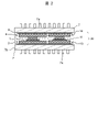
- FIG. 1 is an external plan view of a power module according to a first embodiment of the present invention
- excluded the heat radiating member from FIG. 1 is a chip layout diagram of a power semiconductor module according to a first embodiment of the present invention
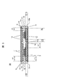
- FIG. 6 is a cross-sectional view of FIG. 5 with the flow path forming body removed; A first modification of FIG. A second modification of FIG. Sectional drawing of the power semiconductor module based on the 3rd Embodiment of this invention. Sectional drawing of the power semiconductor module based on the 4th Embodiment of this invention.
- the heat dissipation member 7 is, for example, a composite material such as Cu, Cu alloy, Cu--C or Cu--CuO, or a composite material such as Al, Al alloy, Al-SiC or Al--C.
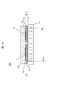
- FIG. 3 is a cross-sectional view of the power semiconductor module with the heat dissipation member removed from FIG.
- the first power semiconductor element 1 and the second power semiconductor element 11 are arranged on the first conductor plate 3 and the second conductor plate 13 respectively such that the first length L1 is longer than the second length L2. ing. More specifically, of the first length L1 and the second length L2, which are approximately the same length as in the conventional configuration, only the second length L2 is reduced. are placed. The reason for this configuration is that thermal stress during driving of the power semiconductor module 30 may cause damage such as peeling or cracking of the insulating layer 5 .
- the first power semiconductor element 1 and the second power semiconductor element 11 are separated from each other by the first conductor plate 3 and the second conductor plate so that the first length L1 is longer than the second length L2. 13, respectively.
- the maximum value of the thermal stress of the insulating layer 5 does not increase, and the effect of the thermal stress on the insulating layer 5 is small because it is joined to the second power semiconductor element 11 having a small amount of heat generation.
- a second length L2 can be determined by reducing the size of the plate 13 alone. By doing so, the reliability of the power module 100 can be ensured while downsizing can be achieved.
- the power semiconductor element 1 , 11 spreads out, the effect of improving the heat dissipation can be obtained.
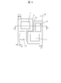
- FIG. 4 is a chip layout diagram of the power semiconductor module according to the first embodiment of the present invention.
- the aspect ratio of the first power semiconductor element 1 is smaller than the aspect ratio of the second power semiconductor element 11 . Also, the first conductor plate 3 and the second conductor plate 13 are arranged adjacent to each other in an L shape.
- the power module 100 has a structure in which the insulating layer 5 is sealed with the sealing resin 9 together with the conductor plates 3, 13, 4, 14, so that when the power semiconductor elements 1, 11 generate heat, The difference in thermal deformation between the conductor plates 3, 13, 4, 14 and the insulating layer 5 caused by the temperature rise is reduced, and the thermal stress generated in the insulating layer 5 connected to the ends 3b, 13b of the conductor plates is also reduced. so damage is less likely to occur. Thereby, a more reliable power semiconductor device can be realized.
- the first conductor plate 3, the second conductor plate 13, the third conductor plate 4, and the fourth conductor plate 14 are each connected to the insulating layer 5A, and the insulating layer 5A dissipates heat through the connecting material 20. It is connected to a member (channel forming body) 17 .
- the heat dissipation member 17 has a flow path 17a through which a cooling medium for dissipating heat from the power semiconductor module 30A flows.
- the surfaces opposite to the surfaces connected to the conductor plates 3, 13, 4, 14 are exposed and fixed with a sealing resin 9A. By doing so, it is possible to seal and fix the power semiconductor module 30A including the insulating layer 5A.
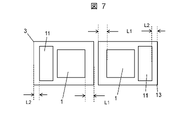
- the power semiconductor element and the conductor plate are arranged in an L shape, but as shown in FIGS. 7 and 8, while maintaining the relationship between the first length L1 and the second length L2, , the first power semiconductor element 1 and the second power semiconductor element 11 can be arranged on the first conductor plate 3 and the second conductor plate 13, respectively.
- the maximum length of the sides of the first power semiconductor element 1 is smaller than the maximum length of the sides of the second power semiconductor element 11 .
- FIG. 9 is a cross-sectional view of a power semiconductor module according to a third embodiment of the invention.
- the power semiconductor module 30B has a configuration in which the first conductor plate 3B is continuous so that both the first power semiconductor element 1 and the second power semiconductor element 11 are arranged as a set.
- the third conductor plate 4B, on which the first power semiconductor element 1 and the second power semiconductor element 11 are connected on the side opposite to the side on which the first conductor plate 3B is connected, is also continuous. configuration. By doing so, only the first length L1 and the second length L2 need to be taken into account when arranging the first power semiconductor element 1 and the second power semiconductor element 11 on the conductor plate. It can be arranged without considering the inward ends 3c, 13c (see FIGS. 3 and 5) of the conductor plate shown in the first embodiment.
- the first length L1 and the second length L2 are larger than the thickness T1 of the first conductor plate, the first power semiconductor element 1 and the second power semiconductor element 11 are Since the heat spreads sufficiently, heat dissipation is improved.
- an example of a 2-in-1 power semiconductor device is shown, but it is also applicable to a 1-in-1 power semiconductor device in which a structure in which an IGBT and a diode are connected one by one on one conductor plate is packaged. It can also be applied to a 6-in-1 power semiconductor device.
- the power semiconductor module 30 of the present embodiment may be connected to the heat dissipation member 7 at both ends of the heat dissipation member 7 .
- FIG. 10 is a cross-sectional view of a power semiconductor module according to a fourth embodiment of the invention.
- the power semiconductor module 30C of the present embodiment has a structure in which the heat dissipation member 17 is provided only on one side for cooling. Along with this, the insulating layer 5 is also installed only on the side where the heat dissipation member 17 is provided, so that a power conversion device that contributes to further miniaturization can be realized.
- a power semiconductor device includes a power semiconductor element, a conductor plate connected to the power semiconductor element, an insulating layer 5 connected to the surface of the conductor plate opposite to the surface connected to the power semiconductor element, It has The power semiconductor device includes a first power semiconductor device 1 and a second power semiconductor device 11 .
- the first distance L1 which is the distance
- the second distance L2 which is the distance from the end of the second power semiconductor element 11 to the end 13b (13c) of the second conductor plate.
- Conductive plates include a first conductive plate 3 connected to the first power semiconductor element 1 and a second conductive plate 13 connected to the second power semiconductor element 11 .
- the first distances L1 and L3 are the cross-sections of the first power semiconductor element 1 passing through the first power semiconductor element 1 and perpendicular to the joint surface between the first conductor plate 3 and the first power semiconductor element 1. It is defined as the distance from the edge to the edge 3b (3c) of the first conductor plate.
- the second distances L2 and L4 are the second power semiconductor element in a cross section perpendicular to the joint surface between the second conductor plate 13 and the second power semiconductor element 11 through the second power semiconductor element 11. 11 to the end 13b (13c) of the second conductor plate.
- the third conductor plate 4 is connected to the surface opposite to the surface to which the first conductor plate 3 is connected.
- a fourth conductor plate 14 is connected to the surface opposite to the surface to which the second conductor plate 13 is connected.
- the surface opposite to the surface connected to the element 1 and the second power semiconductor element 11 is connected to the heat dissipation member 7 via the insulating layer 5 . By doing so, the power module 100 can be cooled on both sides.
- the loss of the first power semiconductor device 1 is greater than the loss of the second power semiconductor device 11 . Because of this arrangement, it is necessary to configure the first distance L1 and the second distance L2 to achieve the effects of the present invention.
- the first power semiconductor element 1 is an IGBT, and the second power semiconductor element 11 is a diode. Because of this arrangement, it is necessary to configure the first distance L1 and the second distance L2 to achieve the effects of the present invention.
- the aspect ratio of the first power semiconductor element 1 is smaller than the aspect ratio of the second power semiconductor element 11 .
- the maximum side length of the first power semiconductor element 1 is smaller than the maximum side length of the second power semiconductor element 11 .
- the first distance L1 is greater than or equal to the third distance L3, and the second distance L2 is greater than or equal to the fourth distance L4.
- the power semiconductor module 30 is connected to the heat dissipation member 7 at both ends of the heat dissipation member 7 .
- the effect of the present invention becomes remarkable at the edge where damage such as peeling or cracking of the insulating layer 5 is likely to occur.
- the ends of the conductor plate can be tapered.
- the insulating layer to which the first conductor plate and the second conductor plate are connected is made flat to provide insulation. It is desirable that the angle from the corner of the end of the conductor plate in contact with the layer toward the end of the power semiconductor element is 45 degrees or less.
- the present invention is not limited to the above embodiments, and various modifications and other configurations can be combined without departing from the spirit of the present invention. Moreover, the present invention is not limited to those having all the configurations described in the above embodiments, and includes those having some of the configurations omitted.
Landscapes
- Cooling Or The Like Of Semiconductors Or Solid State Devices (AREA)
Abstract
Description
図1は、本発明の第1の実施形態に係る、パワーモジュールの外観平面図である。また、図2は、図1のA-A´断面図である。A-A´線はパワー半導体素子を通る断線である。
図5は、本発明の第2の実施形態に係る、パワー半導体モジュールの断面図である。また、図6は、図5から流路形成体を除いた断面図である。
図7および図8は、図4の第1の変形例および第2の変形例である。
図9は、本発明の第3の実施形態に係る、パワー半導体モジュールの断面図である。
図10は、本発明の第4の実施形態に係る、パワー半導体モジュールの断面図である。
3、3B…第1導体板
3b…第1導体板の端部(外向き側)
3c…第1導体板の端部(内向き側)
4、4B…第3導体板
5、5A…絶縁層
7…放熱部材(フィンタイプ)
7a…放熱フィン
7b…放熱部材の端部
9、9A、9C…封止樹脂
10…接合材
11…第2パワー半導体素子
13…第2導体板
13b…第2導体板の端部(外側)
13c…第2導体板の端部(内側)
14…第4導体板
17…放熱部材(流路形成体)
17a…流路
20…接続材(熱伝導体)
30、30A~30C…パワー半導体モジュール
31…外部端子
100…パワーモジュール
L1~L6…第1~第6の長さ
T1…第1導体板の厚さ
T2…第2導体板の厚さ
Claims (11)
- パワー半導体素子と、
前記パワー半導体素子と接続される導体板と、
前記導体板において前記パワー半導体素子と接続される面とは反対側の面で接続される絶縁層と、を備えたパワー半導体装置であって、
前記パワー半導体素子は、第1のパワー半導体素子と、第2のパワー半導体素子と、を含み、
前記第1のパワー半導体素子の発熱量が前記第2のパワー半導体素子の発熱量よりも大きい場合、前記第1のパワー半導体素子の端部から前記導体板の端部までの距離である第1の距離は、前記第2のパワー半導体素子の端部から前記導体板の端部までの距離である第2の距離よりも大きい
パワー半導体装置。 - 請求項1に記載のパワー半導体装置であって、
前記導体板は、前記第1のパワー半導体素子と接続される第1の導体板と、前記第2のパワー半導体素子と接続される第2の導体板と、を含み、
前記第1の距離は、前記第1のパワー半導体素子を通って前記第1の導体板と前記第1のパワー半導体素子との接合面に垂直な断面における前記第1のパワー半導体素子の前記端部から前記第1の導体板の前記端部までの距離として定義され、
前記第2の距離は、前記第2のパワー半導体素子を通って前記第2の導体板と前記第2のパワー半導体素子との接合面に垂直な断面における前記第2のパワー半導体素子の前記端部から前記第2の導体板の前記端部までの距離として定義される
パワー半導体装置。 - 請求項1に記載のパワー半導体装置であって、
前記第1のパワー半導体素子および前記第2のパワー半導体素子は、同一の前記導体板上に配置され、
前記第1の距離は、前記第1のパワー半導体素子を通って前記導体板と前記第1のパワー半導体素子との接合面に垂直な断面における前記第1のパワー半導体素子の前記端部から前記導体板の前記端部までの距離として定義され、
前記第2の距離は、前記第2のパワー半導体素子を通って前記導体板と前記第2のパワー半導体素子との接合面に垂直な断面における前記第2のパワー半導体素子の前記端部から前記導体板の前記端部までの距離として定義される
パワー半導体装置。 - 請求項1に記載のパワー半導体装置であって、
前記第1のパワー半導体素子において、前記第1の導体板が接続される面とは反対側の面に第3の導体板が接続され、
前記第2のパワー半導体素子において、前記第2の導体板が接続される面とは反対側の面に第4の導体板が接続され、
前記第1から前記第4の導体板において、それぞれ前記第1および前記第2パワー半導体素子と接続される面とは反対側の面で、前記絶縁層を介して放熱部材と接続される
パワー半導体装置。 - 請求項1に記載のパワー半導体装置であって、
前記第1のパワー半導体素子の損失が、前記第2のパワー半導体素子の損失よりも大きい
パワー半導体装置。 - 請求項1に記載のパワー半導体装置あって、
前記第1のパワー半導体素子はIGBTであり、前記第2のパワー半導体素子はダイオードである
パワー半導体装置。 - 請求項1に記載のパワー半導体装置であって、
前記第1のパワー半導体素子の縦横比が、前記第2のパワー半導体素子の縦横比よりも小さい
パワー半導体装置。 - 請求項1に記載のパワー半導体装置であって、
前記第1のパワー半導体素子の辺の長さの最大値は、前記第2のパワー半導体素子の辺の長さの最大値より小さい
パワー半導体装置。 - 請求項4に記載のパワー半導体装置であって、
前記第1のパワー半導体素子の端部から前記第3の導体板の端部までの距離である第3の距離は、前記第2のパワー半導体素子の端部から前記第4の導体板の端部までの距離である第4の距離よりも大きい
パワー半導体装置。 - 請求項9に記載のパワー半導体装置であって、
前記第1の距離は、前記第3の距離以上であり、
前記第2の距離は、前記第4の距離以上である
パワー半導体装置。 - 請求項4に記載のパワー半導体装置であって、
前記放熱部材とは、前記放熱部材の両端部で接続されている
パワー半導体装置。
Priority Applications (3)
| Application Number | Priority Date | Filing Date | Title |
|---|---|---|---|
| CN202180092589.0A CN116783707A (zh) | 2021-03-29 | 2021-12-24 | 功率半导体器件 |
| US18/274,747 US12660617B2 (en) | 2021-03-29 | 2021-12-24 | Power semiconductor device |
| DE112021006266.2T DE112021006266T5 (de) | 2021-03-29 | 2021-12-24 | Leistungshalbleitereinrichtung |
Applications Claiming Priority (2)
| Application Number | Priority Date | Filing Date | Title |
|---|---|---|---|
| JP2021056155A JP7587454B2 (ja) | 2021-03-29 | 2021-03-29 | パワー半導体装置 |
| JP2021-056155 | 2021-03-29 |
Publications (1)
| Publication Number | Publication Date |
|---|---|
| WO2022209083A1 true WO2022209083A1 (ja) | 2022-10-06 |
Family
ID=83455782
Family Applications (1)
| Application Number | Title | Priority Date | Filing Date |
|---|---|---|---|
| PCT/JP2021/048274 Ceased WO2022209083A1 (ja) | 2021-03-29 | 2021-12-24 | パワー半導体装置 |
Country Status (5)
| Country | Link |
|---|---|
| US (1) | US12660617B2 (ja) |
| JP (1) | JP7587454B2 (ja) |
| CN (1) | CN116783707A (ja) |
| DE (1) | DE112021006266T5 (ja) |
| WO (1) | WO2022209083A1 (ja) |
Families Citing this family (1)
| Publication number | Priority date | Publication date | Assignee | Title |
|---|---|---|---|---|
| JP7580349B2 (ja) * | 2021-07-01 | 2024-11-11 | 日立Astemo株式会社 | パワー半導体装置 |
Citations (4)
| Publication number | Priority date | Publication date | Assignee | Title |
|---|---|---|---|---|
| JP2002260936A (ja) * | 2001-03-06 | 2002-09-13 | Hitachi Ltd | 内燃機関の点火回路モジュール及び点火コイル装置 |
| JP2009059887A (ja) * | 2007-08-31 | 2009-03-19 | Denso Corp | 電力変換装置 |
| WO2015186470A1 (ja) * | 2014-06-03 | 2015-12-10 | 日立オートモティブシステムズ株式会社 | 半導体モジュールおよび半導体モジュールの製造方法ならびに電子制御装置 |
| WO2020105407A1 (ja) * | 2018-11-21 | 2020-05-28 | 日立オートモティブシステムズ株式会社 | パワー半導体装置 |
Family Cites Families (3)
| Publication number | Priority date | Publication date | Assignee | Title |
|---|---|---|---|---|
| KR101827186B1 (ko) * | 2013-09-04 | 2018-02-07 | 미쓰비시덴키 가부시키가이샤 | 반도체 모듈 및 인버터 장치 |
| DE112016006381B4 (de) * | 2016-02-09 | 2024-06-20 | Mitsubishi Electric Corporation | Leistungshalbleitervorrichtung und herstellungsverfahren dafür |
| JP6710163B2 (ja) | 2017-01-12 | 2020-06-17 | 日立オートモティブシステムズ株式会社 | パワー半導体装置 |
-
2021
- 2021-03-29 JP JP2021056155A patent/JP7587454B2/ja active Active
- 2021-12-24 US US18/274,747 patent/US12660617B2/en active Active
- 2021-12-24 CN CN202180092589.0A patent/CN116783707A/zh active Pending
- 2021-12-24 DE DE112021006266.2T patent/DE112021006266T5/de active Pending
- 2021-12-24 WO PCT/JP2021/048274 patent/WO2022209083A1/ja not_active Ceased
Patent Citations (4)
| Publication number | Priority date | Publication date | Assignee | Title |
|---|---|---|---|---|
| JP2002260936A (ja) * | 2001-03-06 | 2002-09-13 | Hitachi Ltd | 内燃機関の点火回路モジュール及び点火コイル装置 |
| JP2009059887A (ja) * | 2007-08-31 | 2009-03-19 | Denso Corp | 電力変換装置 |
| WO2015186470A1 (ja) * | 2014-06-03 | 2015-12-10 | 日立オートモティブシステムズ株式会社 | 半導体モジュールおよび半導体モジュールの製造方法ならびに電子制御装置 |
| WO2020105407A1 (ja) * | 2018-11-21 | 2020-05-28 | 日立オートモティブシステムズ株式会社 | パワー半導体装置 |
Also Published As
| Publication number | Publication date |
|---|---|
| US12660617B2 (en) | 2026-06-16 |
| US20240096727A1 (en) | 2024-03-21 |
| JP2022153100A (ja) | 2022-10-12 |
| CN116783707A (zh) | 2023-09-19 |
| JP7587454B2 (ja) | 2024-11-20 |
| DE112021006266T5 (de) | 2023-09-14 |
Similar Documents
| Publication | Publication Date | Title |
|---|---|---|
| KR101836658B1 (ko) | 파워 모듈 및 그 제조 방법 | |
| JP5273101B2 (ja) | 半導体モジュールおよびその製造方法 | |
| US20090194862A1 (en) | Semiconductor module and method of manufacturing the same | |
| JP6257478B2 (ja) | 電力用半導体装置 | |
| JP5217884B2 (ja) | 半導体装置 | |
| CN113039636B (zh) | 功率半导体装置 | |
| JP6286543B2 (ja) | パワーモジュール装置、電力変換装置およびパワーモジュール装置の製造方法 | |
| JP3646665B2 (ja) | インバータ装置 | |
| WO2019003718A1 (ja) | パワー半導体装置及びそれを用いた電力変換装置 | |
| JP7030535B2 (ja) | パワー半導体装置 | |
| JP6286541B2 (ja) | パワーモジュール装置及び電力変換装置 | |
| US11735557B2 (en) | Power module of double-faced cooling | |
| JP2010165743A (ja) | 半導体モジュールおよびその製造方法 | |
| JP4935783B2 (ja) | 半導体装置および複合半導体装置 | |
| JP7356402B2 (ja) | パワーモジュール | |
| JP7587454B2 (ja) | パワー半導体装置 | |
| JP2009200258A (ja) | 半導体モジュール | |
| JP2012015167A (ja) | 半導体モジュールおよびその製造方法 | |
| JP2008258448A (ja) | バスバーおよび半導体装置 | |
| JP4158648B2 (ja) | 半導体冷却ユニット | |
| JP4193633B2 (ja) | 半導体冷却ユニット | |
| JP4396366B2 (ja) | 半導体装置 | |
| JP2025127525A (ja) | 半導体装置 | |
| WO2022075199A1 (ja) | 発熱体冷却構造および電力変換装置 |
Legal Events
| Date | Code | Title | Description |
|---|---|---|---|
| 121 | Ep: the epo has been informed by wipo that ep was designated in this application |
Ref document number: 21935230 Country of ref document: EP Kind code of ref document: A1 |
|
| WWE | Wipo information: entry into national phase |
Ref document number: 112021006266 Country of ref document: DE |
|
| WWE | Wipo information: entry into national phase |
Ref document number: 18274747 Country of ref document: US |
|
| WWE | Wipo information: entry into national phase |
Ref document number: 202180092589.0 Country of ref document: CN |
|
| 122 | Ep: pct application non-entry in european phase |
Ref document number: 21935230 Country of ref document: EP Kind code of ref document: A1 |
|
| WWG | Wipo information: grant in national office |
Ref document number: 18274747 Country of ref document: US |