WO2022202747A1 - Ga2O3系単結晶基板並びにGa2O3系単結晶基板の製造方法 - Google Patents
Ga2O3系単結晶基板並びにGa2O3系単結晶基板の製造方法 Download PDFInfo
- Publication number
- WO2022202747A1 WO2022202747A1 PCT/JP2022/012972 JP2022012972W WO2022202747A1 WO 2022202747 A1 WO2022202747 A1 WO 2022202747A1 JP 2022012972 W JP2022012972 W JP 2022012972W WO 2022202747 A1 WO2022202747 A1 WO 2022202747A1
- Authority
- WO
- WIPO (PCT)
- Prior art keywords
- single crystal
- crystal substrate
- plane
- less
- ga2o3
- Prior art date
- Legal status (The legal status is an assumption and is not a legal conclusion. Google has not performed a legal analysis and makes no representation as to the accuracy of the status listed.)
- Ceased
Links
Images



Classifications
-
- C—CHEMISTRY; METALLURGY
- C30—CRYSTAL GROWTH
- C30B—SINGLE-CRYSTAL GROWTH; UNIDIRECTIONAL SOLIDIFICATION OF EUTECTIC MATERIAL OR UNIDIRECTIONAL DEMIXING OF EUTECTOID MATERIAL; REFINING BY ZONE-MELTING OF MATERIAL; PRODUCTION OF A HOMOGENEOUS POLYCRYSTALLINE MATERIAL WITH DEFINED STRUCTURE; SINGLE CRYSTALS OR HOMOGENEOUS POLYCRYSTALLINE MATERIAL WITH DEFINED STRUCTURE; AFTER-TREATMENT OF SINGLE CRYSTALS OR A HOMOGENEOUS POLYCRYSTALLINE MATERIAL WITH DEFINED STRUCTURE; APPARATUS THEREFOR
- C30B29/00—Single crystals or homogeneous polycrystalline material with defined structure characterised by the material or by their shape
- C30B29/10—Inorganic compounds or compositions
- C30B29/16—Oxides
-
- C—CHEMISTRY; METALLURGY
- C30—CRYSTAL GROWTH
- C30B—SINGLE-CRYSTAL GROWTH; UNIDIRECTIONAL SOLIDIFICATION OF EUTECTIC MATERIAL OR UNIDIRECTIONAL DEMIXING OF EUTECTOID MATERIAL; REFINING BY ZONE-MELTING OF MATERIAL; PRODUCTION OF A HOMOGENEOUS POLYCRYSTALLINE MATERIAL WITH DEFINED STRUCTURE; SINGLE CRYSTALS OR HOMOGENEOUS POLYCRYSTALLINE MATERIAL WITH DEFINED STRUCTURE; AFTER-TREATMENT OF SINGLE CRYSTALS OR A HOMOGENEOUS POLYCRYSTALLINE MATERIAL WITH DEFINED STRUCTURE; APPARATUS THEREFOR
- C30B29/00—Single crystals or homogeneous polycrystalline material with defined structure characterised by the material or by their shape
- C30B29/10—Inorganic compounds or compositions
- C30B29/38—Nitrides
-
- C—CHEMISTRY; METALLURGY
- C30—CRYSTAL GROWTH
- C30B—SINGLE-CRYSTAL GROWTH; UNIDIRECTIONAL SOLIDIFICATION OF EUTECTIC MATERIAL OR UNIDIRECTIONAL DEMIXING OF EUTECTOID MATERIAL; REFINING BY ZONE-MELTING OF MATERIAL; PRODUCTION OF A HOMOGENEOUS POLYCRYSTALLINE MATERIAL WITH DEFINED STRUCTURE; SINGLE CRYSTALS OR HOMOGENEOUS POLYCRYSTALLINE MATERIAL WITH DEFINED STRUCTURE; AFTER-TREATMENT OF SINGLE CRYSTALS OR A HOMOGENEOUS POLYCRYSTALLINE MATERIAL WITH DEFINED STRUCTURE; APPARATUS THEREFOR
- C30B15/00—Single-crystal growth by pulling from a melt, e.g. Czochralski method
- C30B15/34—Edge-defined film-fed crystal-growth using dies or slits
-
- C—CHEMISTRY; METALLURGY
- C30—CRYSTAL GROWTH
- C30B—SINGLE-CRYSTAL GROWTH; UNIDIRECTIONAL SOLIDIFICATION OF EUTECTIC MATERIAL OR UNIDIRECTIONAL DEMIXING OF EUTECTOID MATERIAL; REFINING BY ZONE-MELTING OF MATERIAL; PRODUCTION OF A HOMOGENEOUS POLYCRYSTALLINE MATERIAL WITH DEFINED STRUCTURE; SINGLE CRYSTALS OR HOMOGENEOUS POLYCRYSTALLINE MATERIAL WITH DEFINED STRUCTURE; AFTER-TREATMENT OF SINGLE CRYSTALS OR A HOMOGENEOUS POLYCRYSTALLINE MATERIAL WITH DEFINED STRUCTURE; APPARATUS THEREFOR
- C30B25/00—Single-crystal growth by chemical reaction of reactive gases, e.g. chemical vapour-deposition growth
- C30B25/02—Epitaxial-layer growth
- C30B25/18—Epitaxial-layer growth characterised by the substrate
-
- C—CHEMISTRY; METALLURGY
- C30—CRYSTAL GROWTH
- C30B—SINGLE-CRYSTAL GROWTH; UNIDIRECTIONAL SOLIDIFICATION OF EUTECTIC MATERIAL OR UNIDIRECTIONAL DEMIXING OF EUTECTOID MATERIAL; REFINING BY ZONE-MELTING OF MATERIAL; PRODUCTION OF A HOMOGENEOUS POLYCRYSTALLINE MATERIAL WITH DEFINED STRUCTURE; SINGLE CRYSTALS OR HOMOGENEOUS POLYCRYSTALLINE MATERIAL WITH DEFINED STRUCTURE; AFTER-TREATMENT OF SINGLE CRYSTALS OR A HOMOGENEOUS POLYCRYSTALLINE MATERIAL WITH DEFINED STRUCTURE; APPARATUS THEREFOR
- C30B25/00—Single-crystal growth by chemical reaction of reactive gases, e.g. chemical vapour-deposition growth
- C30B25/02—Epitaxial-layer growth
- C30B25/18—Epitaxial-layer growth characterised by the substrate
- C30B25/183—Epitaxial-layer growth characterised by the substrate being provided with a buffer layer, e.g. a lattice matching layer
-
- C—CHEMISTRY; METALLURGY
- C30—CRYSTAL GROWTH
- C30B—SINGLE-CRYSTAL GROWTH; UNIDIRECTIONAL SOLIDIFICATION OF EUTECTIC MATERIAL OR UNIDIRECTIONAL DEMIXING OF EUTECTOID MATERIAL; REFINING BY ZONE-MELTING OF MATERIAL; PRODUCTION OF A HOMOGENEOUS POLYCRYSTALLINE MATERIAL WITH DEFINED STRUCTURE; SINGLE CRYSTALS OR HOMOGENEOUS POLYCRYSTALLINE MATERIAL WITH DEFINED STRUCTURE; AFTER-TREATMENT OF SINGLE CRYSTALS OR A HOMOGENEOUS POLYCRYSTALLINE MATERIAL WITH DEFINED STRUCTURE; APPARATUS THEREFOR
- C30B25/00—Single-crystal growth by chemical reaction of reactive gases, e.g. chemical vapour-deposition growth
- C30B25/02—Epitaxial-layer growth
- C30B25/18—Epitaxial-layer growth characterised by the substrate
- C30B25/186—Epitaxial-layer growth characterised by the substrate being specially pre-treated by, e.g. chemical or physical means
-
- C—CHEMISTRY; METALLURGY
- C30—CRYSTAL GROWTH
- C30B—SINGLE-CRYSTAL GROWTH; UNIDIRECTIONAL SOLIDIFICATION OF EUTECTIC MATERIAL OR UNIDIRECTIONAL DEMIXING OF EUTECTOID MATERIAL; REFINING BY ZONE-MELTING OF MATERIAL; PRODUCTION OF A HOMOGENEOUS POLYCRYSTALLINE MATERIAL WITH DEFINED STRUCTURE; SINGLE CRYSTALS OR HOMOGENEOUS POLYCRYSTALLINE MATERIAL WITH DEFINED STRUCTURE; AFTER-TREATMENT OF SINGLE CRYSTALS OR A HOMOGENEOUS POLYCRYSTALLINE MATERIAL WITH DEFINED STRUCTURE; APPARATUS THEREFOR
- C30B29/00—Single crystals or homogeneous polycrystalline material with defined structure characterised by the material or by their shape
- C30B29/10—Inorganic compounds or compositions
- C30B29/40—AIIIBV compounds wherein A is B, Al, Ga, In or Tl and B is N, P, As, Sb or Bi
- C30B29/403—AIII-nitrides
-
- H—ELECTRICITY
- H10—SEMICONDUCTOR DEVICES; ELECTRIC SOLID-STATE DEVICES NOT OTHERWISE PROVIDED FOR
- H10D—INORGANIC ELECTRIC SEMICONDUCTOR DEVICES
- H10D30/00—Field-effect transistors [FET]
- H10D30/60—Insulated-gate field-effect transistors [IGFET]
- H10D30/64—Double-diffused metal-oxide semiconductor [DMOS] FETs
- H10D30/66—Vertical DMOS [VDMOS] FETs
-
- H—ELECTRICITY
- H10—SEMICONDUCTOR DEVICES; ELECTRIC SOLID-STATE DEVICES NOT OTHERWISE PROVIDED FOR
- H10D—INORGANIC ELECTRIC SEMICONDUCTOR DEVICES
- H10D62/00—Semiconductor bodies, or regions thereof, of devices having potential barriers
- H10D62/80—Semiconductor bodies, or regions thereof, of devices having potential barriers characterised by the materials
-
- H—ELECTRICITY
- H10—SEMICONDUCTOR DEVICES; ELECTRIC SOLID-STATE DEVICES NOT OTHERWISE PROVIDED FOR
- H10D—INORGANIC ELECTRIC SEMICONDUCTOR DEVICES
- H10D62/00—Semiconductor bodies, or regions thereof, of devices having potential barriers
- H10D62/80—Semiconductor bodies, or regions thereof, of devices having potential barriers characterised by the materials
- H10D62/85—Semiconductor bodies, or regions thereof, of devices having potential barriers characterised by the materials being Group III-V materials, e.g. GaAs
- H10D62/8503—Nitride Group III-V materials, e.g. AlN or GaN
-
- H—ELECTRICITY
- H10—SEMICONDUCTOR DEVICES; ELECTRIC SOLID-STATE DEVICES NOT OTHERWISE PROVIDED FOR
- H10H—INORGANIC LIGHT-EMITTING SEMICONDUCTOR DEVICES HAVING POTENTIAL BARRIERS
- H10H20/00—Individual inorganic light-emitting semiconductor devices having potential barriers, e.g. light-emitting diodes [LED]
- H10H20/80—Constructional details
- H10H20/81—Bodies
- H10H20/815—Bodies having stress relaxation structures, e.g. buffer layers
-
- H—ELECTRICITY
- H10—SEMICONDUCTOR DEVICES; ELECTRIC SOLID-STATE DEVICES NOT OTHERWISE PROVIDED FOR
- H10P—GENERIC PROCESSES OR APPARATUS FOR THE MANUFACTURE OR TREATMENT OF DEVICES COVERED BY CLASS H10
- H10P14/00—Formation of materials, e.g. in the shape of layers or pillars
- H10P14/60—Formation of materials, e.g. in the shape of layers or pillars of insulating materials
- H10P14/69—Inorganic materials
- H10P14/692—Inorganic materials composed of oxides, glassy oxides or oxide-based glasses
- H10P14/6938—Inorganic materials composed of oxides, glassy oxides or oxide-based glasses the material containing at least one metal element, e.g. metal oxides, metal oxynitrides or metal oxycarbides
- H10P14/6939—Inorganic materials composed of oxides, glassy oxides or oxide-based glasses the material containing at least one metal element, e.g. metal oxides, metal oxynitrides or metal oxycarbides characterised by the metal
- H10P14/69391—Inorganic materials composed of oxides, glassy oxides or oxide-based glasses the material containing at least one metal element, e.g. metal oxides, metal oxynitrides or metal oxycarbides characterised by the metal the material containing aluminium, e.g. Al2O3
-
- H—ELECTRICITY
- H10—SEMICONDUCTOR DEVICES; ELECTRIC SOLID-STATE DEVICES NOT OTHERWISE PROVIDED FOR
- H10P—GENERIC PROCESSES OR APPARATUS FOR THE MANUFACTURE OR TREATMENT OF DEVICES COVERED BY CLASS H10
- H10P90/00—Preparation of wafers not covered by a single main group of this subclass, e.g. wafer reinforcement
- H10P90/12—Preparing bulk and homogeneous wafers
-
- H—ELECTRICITY
- H10—SEMICONDUCTOR DEVICES; ELECTRIC SOLID-STATE DEVICES NOT OTHERWISE PROVIDED FOR
- H10W—GENERIC PACKAGES, INTERCONNECTIONS, CONNECTORS OR OTHER CONSTRUCTIONAL DETAILS OF DEVICES COVERED BY CLASS H10
- H10W70/00—Package substrates; Interposers; Redistribution layers [RDL]
- H10W70/60—Insulating or insulated package substrates; Interposers; Redistribution layers
- H10W70/67—Insulating or insulated package substrates; Interposers; Redistribution layers characterised by their insulating layers or insulating parts
- H10W70/69—Insulating materials thereof
- H10W70/698—Semiconductor materials that are electrically insulating, e.g. undoped silicon
-
- H—ELECTRICITY
- H10—SEMICONDUCTOR DEVICES; ELECTRIC SOLID-STATE DEVICES NOT OTHERWISE PROVIDED FOR
- H10D—INORGANIC ELECTRIC SEMICONDUCTOR DEVICES
- H10D30/00—Field-effect transistors [FET]
- H10D30/01—Manufacture or treatment
- H10D30/021—Manufacture or treatment of FETs having insulated gates [IGFET]
- H10D30/025—Manufacture or treatment of FETs having insulated gates [IGFET] of vertical IGFETs
-
- H—ELECTRICITY
- H10—SEMICONDUCTOR DEVICES; ELECTRIC SOLID-STATE DEVICES NOT OTHERWISE PROVIDED FOR
- H10P—GENERIC PROCESSES OR APPARATUS FOR THE MANUFACTURE OR TREATMENT OF DEVICES COVERED BY CLASS H10
- H10P14/00—Formation of materials, e.g. in the shape of layers or pillars
- H10P14/20—Formation of materials, e.g. in the shape of layers or pillars of semiconductor materials
- H10P14/29—Formation of materials, e.g. in the shape of layers or pillars of semiconductor materials characterised by the substrates
- H10P14/2901—Materials
- H10P14/2918—Materials being semiconductor metal oxides
-
- H—ELECTRICITY
- H10—SEMICONDUCTOR DEVICES; ELECTRIC SOLID-STATE DEVICES NOT OTHERWISE PROVIDED FOR
- H10P—GENERIC PROCESSES OR APPARATUS FOR THE MANUFACTURE OR TREATMENT OF DEVICES COVERED BY CLASS H10
- H10P14/00—Formation of materials, e.g. in the shape of layers or pillars
- H10P14/20—Formation of materials, e.g. in the shape of layers or pillars of semiconductor materials
- H10P14/29—Formation of materials, e.g. in the shape of layers or pillars of semiconductor materials characterised by the substrates
- H10P14/2926—Crystal orientations
-
- H—ELECTRICITY
- H10—SEMICONDUCTOR DEVICES; ELECTRIC SOLID-STATE DEVICES NOT OTHERWISE PROVIDED FOR
- H10P—GENERIC PROCESSES OR APPARATUS FOR THE MANUFACTURE OR TREATMENT OF DEVICES COVERED BY CLASS H10
- H10P14/00—Formation of materials, e.g. in the shape of layers or pillars
- H10P14/20—Formation of materials, e.g. in the shape of layers or pillars of semiconductor materials
- H10P14/32—Formation of materials, e.g. in the shape of layers or pillars of semiconductor materials characterised by intermediate layers between substrates and deposited layers
- H10P14/3202—Materials thereof
- H10P14/3214—Materials thereof being Group IIIA-VA semiconductors
- H10P14/3216—Nitrides
-
- H—ELECTRICITY
- H10—SEMICONDUCTOR DEVICES; ELECTRIC SOLID-STATE DEVICES NOT OTHERWISE PROVIDED FOR
- H10P—GENERIC PROCESSES OR APPARATUS FOR THE MANUFACTURE OR TREATMENT OF DEVICES COVERED BY CLASS H10
- H10P14/00—Formation of materials, e.g. in the shape of layers or pillars
- H10P14/20—Formation of materials, e.g. in the shape of layers or pillars of semiconductor materials
- H10P14/32—Formation of materials, e.g. in the shape of layers or pillars of semiconductor materials characterised by intermediate layers between substrates and deposited layers
- H10P14/3242—Structure
- H10P14/3244—Layer structure
- H10P14/3251—Layer structure consisting of three or more layers
-
- H—ELECTRICITY
- H10—SEMICONDUCTOR DEVICES; ELECTRIC SOLID-STATE DEVICES NOT OTHERWISE PROVIDED FOR
- H10P—GENERIC PROCESSES OR APPARATUS FOR THE MANUFACTURE OR TREATMENT OF DEVICES COVERED BY CLASS H10
- H10P14/00—Formation of materials, e.g. in the shape of layers or pillars
- H10P14/20—Formation of materials, e.g. in the shape of layers or pillars of semiconductor materials
- H10P14/34—Deposited materials, e.g. layers
- H10P14/3402—Deposited materials, e.g. layers characterised by the chemical composition
- H10P14/3414—Deposited materials, e.g. layers characterised by the chemical composition being group IIIA-VIA materials
- H10P14/3416—Nitrides
-
- H—ELECTRICITY
- H10—SEMICONDUCTOR DEVICES; ELECTRIC SOLID-STATE DEVICES NOT OTHERWISE PROVIDED FOR
- H10P—GENERIC PROCESSES OR APPARATUS FOR THE MANUFACTURE OR TREATMENT OF DEVICES COVERED BY CLASS H10
- H10P14/00—Formation of materials, e.g. in the shape of layers or pillars
- H10P14/20—Formation of materials, e.g. in the shape of layers or pillars of semiconductor materials
- H10P14/34—Deposited materials, e.g. layers
- H10P14/3438—Doping during depositing
- H10P14/3441—Conductivity type
- H10P14/3444—P-type
Definitions
- the present invention relates to a Ga 2 O 3 -based single crystal substrate and a method for producing a Ga 2 O 3 -based single crystal substrate.
- a low-temperature AlN buffer layer is first laminated on a Ga 2 O 3 -based single crystal substrate, and then a nitride semiconductor layer or the like is laminated on the buffer layer to create various device structures. making it possible.
- Patent Document 2 a method of stacking an interfacial resistance reduction layer and then a stress relaxation layer on a low-temperature AlN buffer layer, and stacking an Al x Ga (1-x) N-based semiconductor layer on the stress relaxation layer.
- an Al x Ga (1-x) N-based semiconductor in which cracks in the semiconductor layer are effectively suppressed can be obtained.
- the technology for stacking semiconductors on Ga 2 O 3 -based single crystal substrates is under research and development.
- the crystal system to which a single crystal belongs is one of the most important basic elements.
- Major semiconductor single crystal substrates currently used in various semiconductor devices include, for example, Si substrates, GaAs substrates, SiC(4H) substrates, and sapphire substrates. These crystal systems are cubic, cubic, and hexagonal, respectively. They are crystals and trigonal crystals, both of which are highly symmetrical crystal systems and have weak cleavage.
- the new Ga 2 O 3 system single crystal belongs to the monoclinic crystal system, which is a rare crystal system with low symmetry. , there was a possibility that conventional semiconductor lamination technology would not work.
- the present invention has been made in view of the above problems .
- a manufacturing method for a single crystal substrate, and an Al x Ga (1-x) N-based optical semiconductor device and an Al x Ga (1-x) N-based power semiconductor device using the Ga 2 O 3 -based single crystal substrate With the goal.
- a Ga 2 O 3 -based single crystal substrate having a principal surface with a warp amount of ⁇ 50 ⁇ m or more and 50 ⁇ m or less (including 0 ⁇ m).
- the Ga 2 O 3 -based single crystal substrate according to [1] above which has a circular planar shape, a diameter of 24 mm or more and 160 mm or less, and a thickness of 0.1 mm or more and 2.0 mm or less.
- the Ga 2 O 3 -based single crystal substrate according to [1] above which has a square planar shape, a long side of 15 mm or more and 150 mm or less, and a thickness of 0.1 mm or more and 2.0 mm or less.
- a plane inclined in the range of 7° or less with respect to any of the (100) plane, (010) plane, (001) plane, (-201) plane, and (101) plane is the main surface of the Ga 2 O 3 system single crystal substrate according to any one of [1] to [4] above.
- the principal plane is the (100) plane or a plane inclined by 7° or less from the (100) plane, perpendicular to the principal plane and parallel to the b-axis or within a range of 5°.
- the Ga 2 O 3 -based single crystal substrate according to any one of [1] to [6] above, wherein at least one inclined end surface is provided.
- the main surface is other than the (100) plane or a plane inclined in the range of 7° or less from a plane other than the (100) plane, is perpendicular to the above main surface, and is both the main surface and the (100) plane.
- the Ga 2 O 3 single crystal according to any one of the above [1] to [6], which has at least one end face that is parallel to or inclined within the range of 5° from a direction parallel to the line of intersection with substrate.
- [11] Contains a p-type dopant, Group 1 element, Group 2 element, Group 15 element, or one or more elements of Fe, Cu, and Zn, in a total range of 0.02 mol% or more and 0.15 mol% or less.
- the Ga 2 O 3 -based single crystal substrate according to any one of [1] to [9] above.
- Ga2O3 - based single crystal substrate according to [13] above, wherein the Ga2O3 - based epitaxial layer or the AlGaN-based epitaxial layer has a thickness of 1 nm or more and 50 ⁇ m or less.
- the direction in which the Ga 2 O 3 single crystal is grown is 7° to any one of the a-axis, b-axis, and c-axis directions, or any one of the a-axis, b-axis, and c-axis directions.
- the Ga 2 O 3 single crystal substrate of the present invention When the Ga 2 O 3 single crystal substrate of the present invention is used as a base substrate, it is possible to eliminate cracks and peeling that occur during the lamination step of Al x Ga (1-x) N semiconductors, and to prevent warping during lamination. It was found that high-quality and uniform Al x Ga (1-x) N-based semiconductor laminated films can be grown because the temperature distribution in the substrate surface can be made uniform because the temperature can be kept small. As a result, for example, Al x Ga (1-x) N-based ultraviolet LEDs, which are a type of optical semiconductor device, can be manufactured with high quality, and more ultraviolet LED elements can be obtained from a single substrate. Therefore, the yield increases. Furthermore, it is possible to manufacture ultraviolet LEDs on large substrates, which improves productivity. Also, the same applies to power semiconductor devices.
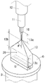
- FIG. 1 is a schematic cross-sectional view illustrating a growth furnace as an example of a method for producing a Ga 2 O 3 -based single crystal by the EFG method.
- FIG. FIG. 2 is an explanatory diagram of a method for producing a Ga 2 O 3 -based single crystal by the EFG method; 1 is a perspective view showing an example of a Ga 2 O 3 -based single crystal substrate according to an embodiment of the present invention;
- FIG. FIG. 2 is a perspective view showing another example of a Ga 2 O 3 -based single crystal substrate according to an embodiment of the present invention;
- FIG. 5 is an explanatory diagram showing measurement standards of SORI in the Ga 2 O 3 -based single crystal substrates of FIGS. 3 and 4.
- FIG. FIG. 6 is an explanatory diagram showing the measurement criteria of the BOW shown in FIG. 5; Structure of UV LED (Example 3). Structure of vertical MISFET (Example 4).
- the Ga 2 O 3 system is ⁇ -type Ga 2 O 3 or ⁇ -Ga 2 O 3 containing Al.
- it contains Al, it is a crystal having a composition ratio of (Al 1-x Ga x ) 2 O 3 (0 ⁇ X ⁇ 1).
- FIG. 1 is a schematic cross-sectional view showing the structure of a Ga 2 O 3 -based single crystal growth apparatus 1 using the EFG method.
- the crystal growth method is not limited to the EFG method, and may be the CZ (Czochralski) method, the Bridgman method, or the Flux method.
- a crucible 3 filled with a Ga 2 O 3 -based single crystal raw material and a die 5 provided with a slit 5A are installed in the crucible 3 inside the growth apparatus 1 .
- a lid 6 is placed on the upper surface of the crucible 3 except for the die 5 portion.
- the Ga 2 O 3 raw material to be used is Ga 2 O 3 having a high purity of 5N (99.999%) or higher, preferably 6N (99.9999%) or higher, and having a high bulk density.
- various additives are added to the raw material. good too.
- an n-type dopant one or more elements of group 14 and group 17 elements are introduced.
- a p-type dopant one or more elements of Groups 1, 2, and 15 and Fe, Cu, and Zn are introduced.
- a high-melting-point material that does not easily react with steam and has heat resistance above about 1800°C is used.
- iridium is the most suitable material, so iridium is used. Therefore, the growth atmosphere must be an inert atmosphere containing 100 vol.
- the crucible 3 may be pressurized to suppress evaporation of raw materials.
- the crucible 3 is induction-heated to a predetermined temperature by a heater section 9 consisting of an induction heating coil, the raw material in the crucible 3 is melted, and the melt rises through the slit 5A due to capillary action.
- a heating method for crystal growth there is resistance heating, which is generally used for growing Si single crystals by the CZ method, but induction heating is more suitable for growing Ga 2 O 3 single crystals.
- induction heating is more suitable for growing Ga 2 O 3 single crystals.
- Ga 2 O 3 is highly susceptible to sublimation and evaporation at high temperatures. Since sublimation and decomposition/evaporation occur from the grown crystals, those crystals become thin and thin, and in the worst case, all the crystals sublimate, decompose/evaporate, and disappear. As a result, the yield of crystal growth is lowered, or the crystal cannot be grown.
- the seed crystal 10 is lowered above the slit 5A so that it partially contacts the die upper surface 5B where the melt 2 is exposed. After that, by pulling the seed crystal 10 at a predetermined speed, crystallization is started from the melt contact portion of the seed crystal 10 .
- the direction of pulling is the direction of crystal growth.
- the temperature is raised as high as possible, and the seed crystal 10 is pulled up while adjusting the pulling speed to form a thin neck for removing dislocations in the crystal (necking 13a).
- the growth temperature is set to 1800° C. or higher, and the thickness of the neck portion is set to about half or less of the cross-sectional area of the seed crystal 10 in contact with the die upper surface portion 5B.
- the seed crystal preferably has as few dislocations as possible in order to obtain a single crystal with few dislocations.
- the rising speed of the seed crystal holder 11 is set to a predetermined speed, and the growth temperature is lowered at a predetermined rate so that the Ga 2 O 3 system single crystal 13 is spread over the width of the die 5 around the seed crystal 10 .
- the crystal is grown so as to widen at a constant angle ⁇ in the direction (spreading 13b).
- ⁇ ° is increased, atoms in the melt are rapidly aligned and crystallized, resulting in more twin crystals. Specifically, when the angle is set to 30° or less, twin crystals disappear and a single crystal with high crystallinity can be grown.
- the impurity concentration in the single crystal is 0.02 mol % or more, twin crystals do not occur regardless of the magnitude of ⁇ . Twin crystals occur when the impurity concentration is lower than 0.02 mol %. Note that when the impurity concentration is higher than 0.15 mol %, the crystallinity deteriorates although twin crystals do not occur. Therefore, the impurity concentration is preferably 0.15 mol % or less.
- the portion (straight body portion 13c) having the same width shape as the full width of the die 5 is pulled up to an appropriate length.
- the substrate is pulled up by about 55 mm at 10 mm/hr.
- the dislocation density of the Ga 2 O 3 system single crystal 13 can be reduced to 1.0 ⁇ 10 5 /cm 2 or less by necking, spreading and growing the straight body portion.
- the pulling plane orientation can be set in various ways according to the plane orientation of the main surface.
- the pulling direction should be 7° or less with respect to any one of the a-axis, b-axis, and c-axis where crystallization is easy during crystal growth and cracks, peeling, and chipping are less likely to occur during substrate processing. Pull up in any direction inclined within the range of .
- the main surface 15 of the substrate 16 or 21 is the (100) plane, which enables formation of a high-quality semiconductor layer with good surface morphology on the main surface 15 and is suitable for fabricating device structures such as ultraviolet LEDs.
- a method for processing the grown Ga 2 O 3 system single crystal 13 into a circular Ga 2 O 3 system single crystal substrate 16 as shown in FIG. 3 or a square shape 21 as shown in FIG. 4 will be described.
- a slicing machine, a core drill, an ultrasonic processing machine, or the like is used to cut out a circular or rectangular shape to produce a circular or rectangular substrate of a predetermined size.
- the end face of the substrate is shaped using an end face grinder.
- orientation flats may be formed on the substrate 16 or 21 as necessary.
- the main surface is the (100) plane or a surface inclined in the range of 7° or less from the (100) plane, it is perpendicular to the main surface and parallel to the b axis or 5° from the b axis is provided as an orientation flat.
- the above principal plane is other than the (100) plane or a plane inclined in the range of 7° or less from the (100) plane, the An end face is provided in a direction parallel to or inclined within a range of 5° from the parallel direction.
- One or more orientation flats may be provided on the main surface as shown in FIG. 3(b).
- one or more corner cutouts may be provided by using the end face of the corner cutout portion as an orientation flat as shown in FIG. 4(b).
- one side of the manufactured substrate 16 or 21 is used as the main surface 15, and the main surface 15 is subjected to polishing processing such as lapping and polishing to make the main surface 15 super flat. Further, the rear surface 19 is also subjected to polishing according to necessity such as shape, and at the same time the thickness of the substrate 16 or 21 is adjusted.
- Abrasive grains for lapping use silicon carbide or alumina. Chemical mechanical polishing is used for polishing, and colloidal silica is used for CMP abrasive grains.
- the surface roughness Ra of the main surface 15 is 3.0 nm or less, and the surface roughness Ra of the back surface 19 is 0.1 nm or more as required.
- the purpose is to remove residual thermal strain, residual processing strain, and coloring, which are common to those skilled in the field of substrate processing such as Si, GaAs, and sapphire single crystal, and to improve electrical characteristics.
- a heat treatment for the purpose is carried out as appropriate.
- the atmosphere gas for heat treatment may be nitrogen, carbon dioxide, argon, oxygen, or air, excluding a reducing gas such as hydrogen gas, which has the effect of roughening the substrate surface, and may be appropriately combined.
- the treatment temperature is 500-1600°C, preferably 700-1400°C. Also, it may be pressurized.
- the shape of the substrate in the plane direction is rectangular, circular, or rectangular or circular with an orientation flat.
- the long side is 15 mm from the viewpoint that it is possible to secure the rigidity as, and it has the strength to the extent that it does not cause any inconvenience in handling, and it is possible to prevent cracks, peeling, and chipping.
- 150 mm or less is preferable, and in the case of each circular shape, the diameter is preferably ⁇ 25 mm or more and ⁇ 160 mm or less.
- the thickness of the substrate is preferably 0.10 mm or more and 2.0 mm or less.
- the amount of warpage of the main surface 15 is within the above range due to substrate processing including heat treatment of the substrate 16 or 21 and substrate cleaning.
- the substrate may be subjected to an internal modification process using a laser to achieve the above-described amount of warp.
- the amount of warpage is defined as having an absolute value of SORI (conforming to SEMI standards) and having a ⁇ sign that indicates the direction of warpage.
- the sign of ⁇ can be obtained from the cross-sectional view of the SORI measurement result, BOW measurement, etc.
- the board surface center position is above the reference plane, it is + (convex shape), and when it is below the reference plane, it is - (concave shape). shape).
- the above SORI and BOW are obtained using a flatness measuring device.
- an optical interference measuring device manufactured by NIDEK is used. The measurement is as follows.
- SORI is the maximum distance from the reference plane S on the front surface of the substrate 16 or 21 when the back surface of the substrate 16 or 21 is fixed by suction at one or three points (non-suction) with a suction chuck (not shown). It is the sum of the vertical distances (absolute values) between the point and the lowest point. Since the SORI is the sum of the absolute values of the vertical distances to the highest point and the lowest point, the SORI is always a positive value. Letting A be the vertical distance from the reference plane S to the highest point, and B be the vertical distance from the reference plane S to the lowest point, SORI is defined by Equation 1 below.
- the amount of warpage is -(
- the SORI value is the same as the so-called PV (Peak to Valley) value when the least-squares plane on the main surface 15 is used as the reference plane.
- BOW as shown in FIG. 6, is the point with the maximum absolute value and the opposite sign from the center C of the substrate on the front surface when the back surface of the substrate 16 is adsorbed at one to three points (non-adhered state). (excluding the center C) and the distance from the center C, as shown in FIG. Note that the upper side of the reference plane S is the positive side, and the lower side is the negative side. In FIG. 6, the center C is positioned below the reference plane S, so BOW has a negative value.
- the dislocation density of the substrate 16 or 21 cut from the single crystal grown by the EFG method is 1.0 ⁇ 10 5 /cm 2 or less.
- the dislocation density is measured with a transmission electron microscope (TEM). Also, since the dot-like etch pit density when the substrate is etched corresponds to the dislocation density, etching may be performed for evaluation.
- TEM transmission electron microscope
- the lamination method is not limited to the MOCVD method, such as the Molecular Beam Epitaxy (MBE) method, the Pulse Laser Deposition (PLD) method, and the Hydride Vapor Phase Epitaxy (HVPE) method.
- MBE Molecular Beam Epitaxy
- PLD Pulse Laser Deposition
- HVPE Hydride Vapor Phase Epitaxy
- an Al x Ga (1-x) N semiconductor layer is grown on the buffer layer at, eg, 800 to 1100° C. to a thickness of 100 ⁇ m or less, and the temperature is lowered after the growth is completed.
- the Ga 2 O 3 system single crystal substrate on which the Al x Ga (1-x) N system semiconductor is laminated is taken out, and quality evaluation of cracks and peeling is performed visually and using an optical microscope.
- Ga 2 O 3 -based epitaxial layer or an AlxGa(1-x)N-based epitaxial layer is once laminated on the entire surface or at least the main surface 15 of the substrates 16 and 21 by MOCVD, HVPE, or the like. good.
- MOCVD MOCVD
- HVPE HVPE
- laminating Ga 2 O 3 based epitaxial layers by laminating 50 ⁇ m or less on the main surface 15 , crystal defects are reduced and the surface roughness Ra of the main surface 15 becomes even smaller than the Ra value.
- a higher-quality Al x Ga (1-x) N layer can be laminated on the upper Ga 2 O 3 -based epitaxial layer.
- AlxGa(1-x)N system epitaxial layer lamination of 1 nm or more improves the resistance of the Ga 2 O 3 system single crystal substrate against hydrogen carrier gas, which is essential for normal nitride semiconductor growth. , the deterioration of the substrate can be suppressed. Therefore, a desired high-quality AlxGa (1-x) N -based semiconductor layer can be grown on a Ga2O3 - based single crystal substrate. Then, not only the Al x Ga (1-x) N-based semiconductor layer but also the Al x Ga (1-x) N-based semiconductor laminate including the substrates 16 and 21 can be obtained with high quality.
- the surfaces of the substrates 16 and 21 may be nitrided instead of the Al x Ga (1-x) N epitaxial layer.
- Ga 2 O 3 -based single crystal substrates according to samples 1 to 7 of the present example were formed by cutting out with a core drill from single crystals grown by b-axis pulling by the EFG method. Common conditions for each of the samples 1 to 7 are as follows. The shape of the substrate in the plane direction is circular with one orientation flat as shown in FIG . and contains 0.05mol%. Furthermore, the Ga 2 O 3 -based single crystal substrate had a diameter of 2 inches, a principal plane of (101) plane with an off angle of 0.0°, a thickness of 0.70 mm, and a dislocation density of 4 ⁇ 10 4 /cm 2 of the principal plane. Free.
- the outer shape of the substrate was shaped using a surface grinder. Then, the back surface of the substrate was subjected to lapping only, or lapping and polishing in the same manner as the main surface. Then, the main surface of the substrate was subjected to lapping and polishing. After polishing, organic cleaning, hydrofluoric acid cleaning, and RCA cleaning were performed.
- the amount of warpage of the Ga 2 O 3 single crystal substrate of each example sample was formed as shown in Table 1.
- Comparative example 1 As comparative samples 1 and 2, Ga 2 O 3 system single crystal substrates were processed in the same manner as in Example 1, and formed as shown in Table 2.
- An AlN buffer layer of 3 nm was grown at 550° C. on the main surface of each of the Ga 2 O 3 -based single crystal substrates of Example Samples 1 to 7 and Comparative Example Samples 1 and 2 by the MOCVD method, and then Si-doped n-type Al 0 was grown.
- a crystal of .4Ga0.6N composition was grown at 1050°C to 4um. After that, the temperature was lowered and the sample was taken out from the apparatus after reaching normal temperature.
- X-ray diffraction (XRD) measurement of the Al0.4Ga0.6N film showed that the entire main surface of each sample was the (0001) plane and was epitaxially grown. As a result of the quality evaluation, it was confirmed that neither the Al0.4Ga0.6N layer nor the Ga 2 O 3 system single crystal substrate in Examples 1 to 7 had cracks or peeling.
- Ga 2 O 3 -based single crystal substrates according to Example Samples 8 to 14 were formed by cutting out rectangular single crystals of 20 mm ⁇ 30 mm using a slicing machine from single crystals grown by pulling along the b-axis by the EFG method. Common conditions for each of the samples 8 to 14 are as follows. All of the substrates are rectangular in shape in the planar direction, and the Ga 2 O 3 -based single crystal forming the substrate is a ⁇ -Ga 2 O 3 single crystal, which is doped with 0.05 mol % of Si.
- the main surface of the Ga 2 O 3 single crystal substrate is the (101) plane with an off angle of 0.0°, the thickness is 0.70 mm, the dislocation density of the main surface is 4 ⁇ 10 4 /cm 2 , and the substrate is twin-free.
- Example 1 In the same manner as in Example 1, an AlN buffer layer and then an n-type Al 0.4 Ga 0.6 N composition were formed on the main surface of each of the Ga 2 O 3 -based single crystal substrates of Example Samples 8 to 14 and Comparative Example Samples 3 and 4. A crystal was grown and a sample was taken out after the temperature was lowered. From the X-ray diffraction (XRD) measurement of the Al 0.4 Ga 0.6 N film, it was confirmed that the main surface of all the samples was the (0001) plane and was epitaxially grown. As a result of the quality evaluation, it was confirmed that neither the Al 0.4 Ga 0.6 N layer nor the Ga 2 O 3 system single crystal substrate had cracks or peeling in Examples 8 to 14.
- XRD X-ray diffraction
- Example 3 Among the samples of Example 1, a vertical ultraviolet LED as an optical device was produced by duplicating a sample under the same conditions as Sample 4 in which cracks and peeling did not occur.
- FIG. 1 An example of the laminated structure of the vertical ultraviolet LED 23 is shown in FIG.
- an InAl 0.4 Ga 0.6 N layer 26 which is a Si-doped n-type cladding layer, is grown at 1000° C. to a thickness of 25 nm by MOCVD.
- In is added to improve the luminous efficiency, and its composition ratio is less than 1%.
- the InAl 0.5 Ga 0.5 N barrier layer 27 is set to 6 nm at 1050° C.
- the InAl 0.3 Ga 0.7 N quantum well layer 28 is set to 2 nm at 1050° C.
- the barrier layer and the quantum well layer are separated.
- a multilayer structure grown alternately is grown in three layers as shown in FIG.
- a Mg-doped p-type InAl 0.6 Ga 0.4 N electron blocking layer 29 is grown at 1050° C. to a thickness of 20 nm.
- a Mg-doped p-type InAl 0.5 Ga 0.5 N clad layer 30 is grown at 1050° C. to a thickness of 20 nm.
- a Mg-doped p-type InAl 0.3 Ga 0.7 N contact layer 31 is grown at 1000° C. to a thickness of 10 nm.
- a Ni/Al laminated structure that provides ohmic contact and highly reflects ultraviolet light coming from the light-emitting layer is formed on the p-type contact layer 31.
- n-side electrode 33 As the n-side electrode 33, a Ti/Au laminated structure is formed which is in ohmic contact with the Ga 2 O 3 system single crystal substrate 16 and highly transmits ultraviolet light coming from the light emitting layer side.
- this ultraviolet LED 23 By energizing the n-side electrode 33 and the p-side electrode 32, this ultraviolet LED 23 emitted ultraviolet light from the n-side electrode 33 side.
- the vertical ultraviolet LED 23 which could not be realized on the sapphire substrate, is realized with high quality without causing cracks or peeling. We were able to. Furthermore, since it became possible to produce vertical ultraviolet LEDs 23 on a large-sized substrate, it was possible to improve productivity.
- Example 4 Among the samples of Example 1, the one under the same conditions as Sample 5 in which no cracks or peeling occurred was duplicated, and a vertical metal-insulator-semiconductor field effect transistor (MISFET: Metal-Insulator-Semiconductor), which is a device for high withstand voltage power, was reproduced. field effect transistor).
- MISFET Metal-insulator-semiconductor field effect transistor
- N is ion-implanted into the n-type Al 0.4 Ga 0.6 N layer 25 using an ion implantation apparatus to form the p-type region 35 .
- a source electrode 37 having a Ti/Al laminated structure is formed on the p-type region 35 and the n+ region 36 by a vapor deposition apparatus as shown in FIG. Al2O3, which is a gate insulator 38, is formed on the n-Al 0.4 Ga 0.6 N layer 25, the p-type region 35, and the n + -type region 36 by a vapor deposition apparatus, and a gate electrode is formed on the gate insulator 38.
- Form 39 with Al is shown in FIG. Al2O3, which is a gate insulator 38, is formed on the n-Al 0.4 Ga 0.6 N layer 25, the p-type region 35, and the n + -type region 36 by a vapor deposition apparatus, and a gate electrode is formed on the gate insulator 38.
- the drain electrode 40 is formed with a Ti/Al laminated structure on the Ga 2 O 3 system single crystal side to complete the process.
- the high breakdown voltage vertical MISFET 34 in which the Al (1-x) Ga x N semiconductors are laminated can be prevented from cracking or cracking. It can be manufactured without peeling. Furthermore, the vertical MISFET 34 can be manufactured on a large-sized substrate, and productivity can be improved.
Landscapes
- Chemical & Material Sciences (AREA)
- Organic Chemistry (AREA)
- Engineering & Computer Science (AREA)
- Crystallography & Structural Chemistry (AREA)
- Materials Engineering (AREA)
- Metallurgy (AREA)
- Inorganic Chemistry (AREA)
- Chemical Kinetics & Catalysis (AREA)
- General Chemical & Material Sciences (AREA)
- Crystals, And After-Treatments Of Crystals (AREA)
- Led Devices (AREA)
- Chemical Vapour Deposition (AREA)
- Recrystallisation Techniques (AREA)
Priority Applications (2)
| Application Number | Priority Date | Filing Date | Title |
|---|---|---|---|
| EP22775531.1A EP4317547A4 (en) | 2021-03-24 | 2022-03-22 | GA2O3-BASED MONOCRYSTALLINE SUBSTRATE AND METHOD FOR MANUFACTURING GA2O3-BASED MONOCRYSTALLINE SUBSTRATE |
| US18/472,375 US20240011192A1 (en) | 2021-03-24 | 2023-09-22 | Ga2o3-based single crystal substrate and method of manufacturing ga2o3-based single crystal substrate |
Applications Claiming Priority (2)
| Application Number | Priority Date | Filing Date | Title |
|---|---|---|---|
| JP2021049332A JP7704399B2 (ja) | 2021-03-24 | 2021-03-24 | Ga2O3系単結晶基板並びにAlxGa(1-x)N系半導体積層体の製造方法 |
| JP2021-049332 | 2021-03-24 |
Related Child Applications (1)
| Application Number | Title | Priority Date | Filing Date |
|---|---|---|---|
| US18/472,375 Continuation US20240011192A1 (en) | 2021-03-24 | 2023-09-22 | Ga2o3-based single crystal substrate and method of manufacturing ga2o3-based single crystal substrate |
Publications (1)
| Publication Number | Publication Date |
|---|---|
| WO2022202747A1 true WO2022202747A1 (ja) | 2022-09-29 |
Family
ID=83397419
Family Applications (1)
| Application Number | Title | Priority Date | Filing Date |
|---|---|---|---|
| PCT/JP2022/012972 Ceased WO2022202747A1 (ja) | 2021-03-24 | 2022-03-22 | Ga2O3系単結晶基板並びにGa2O3系単結晶基板の製造方法 |
Country Status (5)
| Country | Link |
|---|---|
| US (1) | US20240011192A1 (https=) |
| EP (1) | EP4317547A4 (https=) |
| JP (2) | JP7704399B2 (https=) |
| TW (1) | TW202302934A (https=) |
| WO (1) | WO2022202747A1 (https=) |
Families Citing this family (1)
| Publication number | Priority date | Publication date | Assignee | Title |
|---|---|---|---|---|
| WO2025250905A1 (en) * | 2024-05-31 | 2025-12-04 | Luxium Solutions, Llc | Apparatus and method for growth of gallium oxide crystal with an offcut |
Citations (5)
| Publication number | Priority date | Publication date | Assignee | Title |
|---|---|---|---|---|
| JP2000211993A (ja) * | 1999-01-22 | 2000-08-02 | Mitsubishi Electric Corp | 半導体ウェハの製造方法、半導体製造装置、および、半導体装置 |
| JP2014199935A (ja) | 2011-04-08 | 2014-10-23 | 株式会社タムラ製作所 | 半導体積層体及びその製造方法、並びに半導体素子 |
| JP2016013931A (ja) * | 2014-06-30 | 2016-01-28 | 株式会社タムラ製作所 | β−Ga2O3系単結晶基板 |
| JP2016013934A (ja) * | 2014-06-30 | 2016-01-28 | 株式会社タムラ製作所 | β−Ga2O3系単結晶基板の製造方法 |
| JP2017157725A (ja) | 2016-03-02 | 2017-09-07 | 株式会社タムラ製作所 | 窒化物半導体テンプレート及びその製造方法、並びに紫外線led |
Family Cites Families (7)
| Publication number | Priority date | Publication date | Assignee | Title |
|---|---|---|---|---|
| KR100787272B1 (ko) * | 2003-02-24 | 2007-12-20 | 각코호진 와세다다이가쿠 | Ga2O3계 발광 소자 및 그 제조 방법 |
| EP2221855A4 (en) * | 2007-11-21 | 2013-08-07 | Mitsubishi Chem Corp | NITRIDE SEMICONDUCTOR AND NITRIDE SEMICONDUCTOR CRYSTAL GROWTH PROCESS |
| JP5051455B2 (ja) | 2008-01-16 | 2012-10-17 | 日立電線株式会社 | エピタキシャル成長用窒化物半導体基板の製造方法 |
| JP5104830B2 (ja) * | 2008-09-08 | 2012-12-19 | 住友電気工業株式会社 | 基板 |
| JP5786179B2 (ja) | 2010-03-12 | 2015-09-30 | 並木精密宝石株式会社 | 酸化ガリウム単結晶及びその製造方法 |
| US9461124B2 (en) * | 2011-09-08 | 2016-10-04 | Tamura Corporation | Ga2O3 semiconductor element |
| JP5747110B1 (ja) * | 2014-06-30 | 2015-07-08 | 株式会社タムラ製作所 | Ga2O3系単結晶基板 |
-
2021
- 2021-03-24 JP JP2021049332A patent/JP7704399B2/ja active Active
-
2022
- 2022-03-07 TW TW111108149A patent/TW202302934A/zh unknown
- 2022-03-22 EP EP22775531.1A patent/EP4317547A4/en active Pending
- 2022-03-22 WO PCT/JP2022/012972 patent/WO2022202747A1/ja not_active Ceased
-
2023
- 2023-09-22 US US18/472,375 patent/US20240011192A1/en active Pending
- 2023-10-18 JP JP2023179430A patent/JP2023184577A/ja active Pending
Patent Citations (5)
| Publication number | Priority date | Publication date | Assignee | Title |
|---|---|---|---|---|
| JP2000211993A (ja) * | 1999-01-22 | 2000-08-02 | Mitsubishi Electric Corp | 半導体ウェハの製造方法、半導体製造装置、および、半導体装置 |
| JP2014199935A (ja) | 2011-04-08 | 2014-10-23 | 株式会社タムラ製作所 | 半導体積層体及びその製造方法、並びに半導体素子 |
| JP2016013931A (ja) * | 2014-06-30 | 2016-01-28 | 株式会社タムラ製作所 | β−Ga2O3系単結晶基板 |
| JP2016013934A (ja) * | 2014-06-30 | 2016-01-28 | 株式会社タムラ製作所 | β−Ga2O3系単結晶基板の製造方法 |
| JP2017157725A (ja) | 2016-03-02 | 2017-09-07 | 株式会社タムラ製作所 | 窒化物半導体テンプレート及びその製造方法、並びに紫外線led |
Non-Patent Citations (1)
| Title |
|---|
| See also references of EP4317547A4 |
Also Published As
| Publication number | Publication date |
|---|---|
| TW202302934A (zh) | 2023-01-16 |
| JP7704399B2 (ja) | 2025-07-08 |
| EP4317547A1 (en) | 2024-02-07 |
| JP2023184577A (ja) | 2023-12-28 |
| EP4317547A4 (en) | 2024-08-21 |
| JP2022147881A (ja) | 2022-10-06 |
| US20240011192A1 (en) | 2024-01-11 |
Similar Documents
| Publication | Publication Date | Title |
|---|---|---|
| TWI429797B (zh) | 第 iii 族氮化物半導體結晶基板及半導體元件 | |
| JP4597259B2 (ja) | Iii族窒化物半導体成長用基板、iii族窒化物半導体エピタキシャル基板、iii族窒化物半導体素子およびiii族窒化物半導体自立基板、ならびに、これらの製造方法 | |
| JP5865440B2 (ja) | β−Ga2O3系単結晶基板の製造方法 | |
| US9349915B2 (en) | β-Ga2O3-based single crystal substrate | |
| JP2022552024A (ja) | ScAlMgO4基板に基づく窒化ガリウム単結晶及びその製造方法 | |
| US11384449B2 (en) | Two-stage seeded growth of large aluminum nitride single crystals | |
| US20240011192A1 (en) | Ga2o3-based single crystal substrate and method of manufacturing ga2o3-based single crystal substrate | |
| WO2004086520A1 (ja) | ZnO系半導体素子およびその製造方法 | |
| JP2017001907A (ja) | β−Ga2O3基板、半導体積層構造体、及び半導体素子 | |
| JP2015164162A (ja) | 半導体積層構造体及び半導体素子 | |
| JP7800516B2 (ja) | 積層体 | |
| EP3435407B1 (en) | Method for producing group iii nitride laminate | |
| JP5145488B2 (ja) | サファイア単結晶基板及びその製造方法 | |
| JP2010251743A (ja) | Iii族窒化物半導体成長用基板、iii族窒化物半導体自立基板、iii族窒化物半導体素子、ならびに、これらの製造方法 | |
| JP7822460B2 (ja) | AlN単結晶基板及びデバイス | |
| JP2023021233A (ja) | Ga2O3系単結晶基板と、Ga2O3系単結晶基板の製造方法 | |
| CN118610071A (zh) | 复合结构氮化铝单晶复合衬底及其制备方法、紫外发光器件 | |
| WO2025196855A1 (ja) | Iii族元素窒化物基板、貼合せ基板、半導体素子およびiii族元素窒化物基板の製造方法 | |
| Bauman et al. | Fabrication and Testing of Substrates Made from Bulk Gallium Oxide Crystals by the Cleavage Method | |
| JP2000247790A (ja) | 半導体素子用基板及び半導体素子並びに窒素化合物半導体単結晶基板の製造方法 | |
| JP2011222778A (ja) | 積層体の製造方法、iii族窒化物単結晶自立基板の製造方法、および、積層体 |
Legal Events
| Date | Code | Title | Description |
|---|---|---|---|
| 121 | Ep: the epo has been informed by wipo that ep was designated in this application |
Ref document number: 22775531 Country of ref document: EP Kind code of ref document: A1 |
|
| WWE | Wipo information: entry into national phase |
Ref document number: 2022775531 Country of ref document: EP |
|
| NENP | Non-entry into the national phase |
Ref country code: DE |
|
| ENP | Entry into the national phase |
Ref document number: 2022775531 Country of ref document: EP Effective date: 20231024 |