WO2022202747A1 - Ga2o3-based single crystal substrate and method for manufacturing ga2o3-based single crystal substrate - Google Patents
Ga2o3-based single crystal substrate and method for manufacturing ga2o3-based single crystal substrate Download PDFInfo
- Publication number
- WO2022202747A1 WO2022202747A1 PCT/JP2022/012972 JP2022012972W WO2022202747A1 WO 2022202747 A1 WO2022202747 A1 WO 2022202747A1 JP 2022012972 W JP2022012972 W JP 2022012972W WO 2022202747 A1 WO2022202747 A1 WO 2022202747A1
- Authority
- WO
- WIPO (PCT)
- Prior art keywords
- single crystal
- crystal substrate
- plane
- less
- ga2o3
- Prior art date
Links
- 239000013078 crystal Substances 0.000 title claims abstract description 171
- 239000000758 substrate Substances 0.000 title claims abstract description 168
- 238000004519 manufacturing process Methods 0.000 title claims abstract description 17
- 238000000034 method Methods 0.000 title abstract description 27
- 239000004065 semiconductor Substances 0.000 claims abstract description 52
- QZQVBEXLDFYHSR-UHFFFAOYSA-N gallium(III) oxide Inorganic materials O=[Ga]O[Ga]=O QZQVBEXLDFYHSR-UHFFFAOYSA-N 0.000 claims abstract description 21
- 238000010438 heat treatment Methods 0.000 claims abstract description 15
- 230000006698 induction Effects 0.000 claims abstract description 7
- 229910005191 Ga 2 O 3 Inorganic materials 0.000 claims description 110
- 229910002704 AlGaN Inorganic materials 0.000 claims description 8
- 239000002019 doping agent Substances 0.000 claims description 6
- 230000003746 surface roughness Effects 0.000 claims description 5
- 229910052800 carbon group element Inorganic materials 0.000 claims description 3
- 229910052802 copper Inorganic materials 0.000 claims description 3
- 238000002109 crystal growth method Methods 0.000 claims description 3
- 229910052736 halogen Inorganic materials 0.000 claims description 3
- 229910052742 iron Inorganic materials 0.000 claims description 3
- 229910052725 zinc Inorganic materials 0.000 claims description 3
- 229910052696 pnictogen Inorganic materials 0.000 claims description 2
- 230000003287 optical effect Effects 0.000 abstract description 7
- 238000005336 cracking Methods 0.000 abstract description 4
- 238000003475 lamination Methods 0.000 description 17
- 238000012545 processing Methods 0.000 description 12
- 238000005231 Edge Defined Film Fed Growth Methods 0.000 description 9
- 230000000052 comparative effect Effects 0.000 description 9
- 238000005498 polishing Methods 0.000 description 9
- 238000004140 cleaning Methods 0.000 description 8
- 238000005259 measurement Methods 0.000 description 7
- 230000008569 process Effects 0.000 description 6
- 239000002994 raw material Substances 0.000 description 6
- 230000008020 evaporation Effects 0.000 description 5
- 238000001704 evaporation Methods 0.000 description 5
- KRHYYFGTRYWZRS-UHFFFAOYSA-N Fluorane Chemical compound F KRHYYFGTRYWZRS-UHFFFAOYSA-N 0.000 description 4
- 238000009826 distribution Methods 0.000 description 4
- 230000005669 field effect Effects 0.000 description 4
- 239000012535 impurity Substances 0.000 description 4
- 239000000155 melt Substances 0.000 description 4
- 238000003892 spreading Methods 0.000 description 4
- 230000007480 spreading Effects 0.000 description 4
- 238000000859 sublimation Methods 0.000 description 4
- 230000008022 sublimation Effects 0.000 description 4
- VYPSYNLAJGMNEJ-UHFFFAOYSA-N Silicium dioxide Chemical compound O=[Si]=O VYPSYNLAJGMNEJ-UHFFFAOYSA-N 0.000 description 3
- 230000004888 barrier function Effects 0.000 description 3
- 230000032798 delamination Effects 0.000 description 3
- 238000010586 diagram Methods 0.000 description 3
- 238000005516 engineering process Methods 0.000 description 3
- 238000002248 hydride vapour-phase epitaxy Methods 0.000 description 3
- 239000012212 insulator Substances 0.000 description 3
- 229910052741 iridium Inorganic materials 0.000 description 3
- GKOZUEZYRPOHIO-UHFFFAOYSA-N iridium atom Chemical compound [Ir] GKOZUEZYRPOHIO-UHFFFAOYSA-N 0.000 description 3
- 238000010030 laminating Methods 0.000 description 3
- 239000000463 material Substances 0.000 description 3
- 230000004048 modification Effects 0.000 description 3
- 238000012986 modification Methods 0.000 description 3
- 238000013441 quality evaluation Methods 0.000 description 3
- 229910052594 sapphire Inorganic materials 0.000 description 3
- 239000010980 sapphire Substances 0.000 description 3
- CSCPPACGZOOCGX-UHFFFAOYSA-N Acetone Chemical compound CC(C)=O CSCPPACGZOOCGX-UHFFFAOYSA-N 0.000 description 2
- XKRFYHLGVUSROY-UHFFFAOYSA-N Argon Chemical compound [Ar] XKRFYHLGVUSROY-UHFFFAOYSA-N 0.000 description 2
- IJGRMHOSHXDMSA-UHFFFAOYSA-N Atomic nitrogen Chemical compound N#N IJGRMHOSHXDMSA-UHFFFAOYSA-N 0.000 description 2
- CURLTUGMZLYLDI-UHFFFAOYSA-N Carbon dioxide Chemical compound O=C=O CURLTUGMZLYLDI-UHFFFAOYSA-N 0.000 description 2
- 229910001218 Gallium arsenide Inorganic materials 0.000 description 2
- UFHFLCQGNIYNRP-UHFFFAOYSA-N Hydrogen Chemical compound [H][H] UFHFLCQGNIYNRP-UHFFFAOYSA-N 0.000 description 2
- 238000002441 X-ray diffraction Methods 0.000 description 2
- 239000006061 abrasive grain Substances 0.000 description 2
- PNEYBMLMFCGWSK-UHFFFAOYSA-N aluminium oxide Inorganic materials [O-2].[O-2].[O-2].[Al+3].[Al+3] PNEYBMLMFCGWSK-UHFFFAOYSA-N 0.000 description 2
- 230000000903 blocking effect Effects 0.000 description 2
- 230000008859 change Effects 0.000 description 2
- 238000002425 crystallisation Methods 0.000 description 2
- 230000008025 crystallization Effects 0.000 description 2
- 238000005520 cutting process Methods 0.000 description 2
- 238000000354 decomposition reaction Methods 0.000 description 2
- 239000007789 gas Substances 0.000 description 2
- 150000004767 nitrides Chemical class 0.000 description 2
- 230000009467 reduction Effects 0.000 description 2
- HBMJWWWQQXIZIP-UHFFFAOYSA-N silicon carbide Chemical compound [Si+]#[C-] HBMJWWWQQXIZIP-UHFFFAOYSA-N 0.000 description 2
- 229910010271 silicon carbide Inorganic materials 0.000 description 2
- 238000007740 vapor deposition Methods 0.000 description 2
- 240000006829 Ficus sundaica Species 0.000 description 1
- 230000009471 action Effects 0.000 description 1
- 239000000654 additive Substances 0.000 description 1
- 239000003570 air Substances 0.000 description 1
- 229910052786 argon Inorganic materials 0.000 description 1
- QVGXLLKOCUKJST-UHFFFAOYSA-N atomic oxygen Chemical compound [O] QVGXLLKOCUKJST-UHFFFAOYSA-N 0.000 description 1
- 230000005540 biological transmission Effects 0.000 description 1
- 230000015572 biosynthetic process Effects 0.000 description 1
- 229910052799 carbon Inorganic materials 0.000 description 1
- 229910002092 carbon dioxide Inorganic materials 0.000 description 1
- 239000001569 carbon dioxide Substances 0.000 description 1
- 239000012159 carrier gas Substances 0.000 description 1
- 230000015556 catabolic process Effects 0.000 description 1
- 238000006243 chemical reaction Methods 0.000 description 1
- 238000005229 chemical vapour deposition Methods 0.000 description 1
- 238000005253 cladding Methods 0.000 description 1
- 238000003776 cleavage reaction Methods 0.000 description 1
- 239000008119 colloidal silica Substances 0.000 description 1
- 238000004040 coloring Methods 0.000 description 1
- 238000011109 contamination Methods 0.000 description 1
- 229910052593 corundum Inorganic materials 0.000 description 1
- 230000007547 defect Effects 0.000 description 1
- 238000000151 deposition Methods 0.000 description 1
- 230000008021 deposition Effects 0.000 description 1
- 230000006866 deterioration Effects 0.000 description 1
- AJNVQOSZGJRYEI-UHFFFAOYSA-N digallium;oxygen(2-) Chemical compound [O-2].[O-2].[O-2].[Ga+3].[Ga+3] AJNVQOSZGJRYEI-UHFFFAOYSA-N 0.000 description 1
- 230000000694 effects Effects 0.000 description 1
- 238000005530 etching Methods 0.000 description 1
- 238000011156 evaluation Methods 0.000 description 1
- 238000007716 flux method Methods 0.000 description 1
- 239000001257 hydrogen Substances 0.000 description 1
- 229910052739 hydrogen Inorganic materials 0.000 description 1
- 239000011810 insulating material Substances 0.000 description 1
- 238000005468 ion implantation Methods 0.000 description 1
- 150000002500 ions Chemical class 0.000 description 1
- 230000008018 melting Effects 0.000 description 1
- 238000002844 melting Methods 0.000 description 1
- 229910052751 metal Inorganic materials 0.000 description 1
- 239000002184 metal Substances 0.000 description 1
- 238000001451 molecular beam epitaxy Methods 0.000 description 1
- 229910052757 nitrogen Inorganic materials 0.000 description 1
- 239000001301 oxygen Substances 0.000 description 1
- 229910052760 oxygen Inorganic materials 0.000 description 1
- 230000000704 physical effect Effects 0.000 description 1
- 238000007517 polishing process Methods 0.000 description 1
- 238000012827 research and development Methods 0.000 description 1
- 230000000630 rising effect Effects 0.000 description 1
- 238000007788 roughening Methods 0.000 description 1
- 230000007017 scission Effects 0.000 description 1
- 239000000377 silicon dioxide Substances 0.000 description 1
- 239000000126 substance Substances 0.000 description 1
- 238000002834 transmittance Methods 0.000 description 1
- 229910001845 yogo sapphire Inorganic materials 0.000 description 1
Images


Classifications
-
- C—CHEMISTRY; METALLURGY
- C30—CRYSTAL GROWTH
- C30B—SINGLE-CRYSTAL GROWTH; UNIDIRECTIONAL SOLIDIFICATION OF EUTECTIC MATERIAL OR UNIDIRECTIONAL DEMIXING OF EUTECTOID MATERIAL; REFINING BY ZONE-MELTING OF MATERIAL; PRODUCTION OF A HOMOGENEOUS POLYCRYSTALLINE MATERIAL WITH DEFINED STRUCTURE; SINGLE CRYSTALS OR HOMOGENEOUS POLYCRYSTALLINE MATERIAL WITH DEFINED STRUCTURE; AFTER-TREATMENT OF SINGLE CRYSTALS OR A HOMOGENEOUS POLYCRYSTALLINE MATERIAL WITH DEFINED STRUCTURE; APPARATUS THEREFOR
- C30B29/00—Single crystals or homogeneous polycrystalline material with defined structure characterised by the material or by their shape
- C30B29/10—Inorganic compounds or compositions
- C30B29/16—Oxides
-
- C—CHEMISTRY; METALLURGY
- C30—CRYSTAL GROWTH
- C30B—SINGLE-CRYSTAL GROWTH; UNIDIRECTIONAL SOLIDIFICATION OF EUTECTIC MATERIAL OR UNIDIRECTIONAL DEMIXING OF EUTECTOID MATERIAL; REFINING BY ZONE-MELTING OF MATERIAL; PRODUCTION OF A HOMOGENEOUS POLYCRYSTALLINE MATERIAL WITH DEFINED STRUCTURE; SINGLE CRYSTALS OR HOMOGENEOUS POLYCRYSTALLINE MATERIAL WITH DEFINED STRUCTURE; AFTER-TREATMENT OF SINGLE CRYSTALS OR A HOMOGENEOUS POLYCRYSTALLINE MATERIAL WITH DEFINED STRUCTURE; APPARATUS THEREFOR
- C30B29/00—Single crystals or homogeneous polycrystalline material with defined structure characterised by the material or by their shape
- C30B29/10—Inorganic compounds or compositions
- C30B29/38—Nitrides
-
- C—CHEMISTRY; METALLURGY
- C30—CRYSTAL GROWTH
- C30B—SINGLE-CRYSTAL GROWTH; UNIDIRECTIONAL SOLIDIFICATION OF EUTECTIC MATERIAL OR UNIDIRECTIONAL DEMIXING OF EUTECTOID MATERIAL; REFINING BY ZONE-MELTING OF MATERIAL; PRODUCTION OF A HOMOGENEOUS POLYCRYSTALLINE MATERIAL WITH DEFINED STRUCTURE; SINGLE CRYSTALS OR HOMOGENEOUS POLYCRYSTALLINE MATERIAL WITH DEFINED STRUCTURE; AFTER-TREATMENT OF SINGLE CRYSTALS OR A HOMOGENEOUS POLYCRYSTALLINE MATERIAL WITH DEFINED STRUCTURE; APPARATUS THEREFOR
- C30B15/00—Single-crystal growth by pulling from a melt, e.g. Czochralski method
- C30B15/34—Edge-defined film-fed crystal-growth using dies or slits
-
- C—CHEMISTRY; METALLURGY
- C30—CRYSTAL GROWTH
- C30B—SINGLE-CRYSTAL GROWTH; UNIDIRECTIONAL SOLIDIFICATION OF EUTECTIC MATERIAL OR UNIDIRECTIONAL DEMIXING OF EUTECTOID MATERIAL; REFINING BY ZONE-MELTING OF MATERIAL; PRODUCTION OF A HOMOGENEOUS POLYCRYSTALLINE MATERIAL WITH DEFINED STRUCTURE; SINGLE CRYSTALS OR HOMOGENEOUS POLYCRYSTALLINE MATERIAL WITH DEFINED STRUCTURE; AFTER-TREATMENT OF SINGLE CRYSTALS OR A HOMOGENEOUS POLYCRYSTALLINE MATERIAL WITH DEFINED STRUCTURE; APPARATUS THEREFOR
- C30B25/00—Single-crystal growth by chemical reaction of reactive gases, e.g. chemical vapour-deposition growth
- C30B25/02—Epitaxial-layer growth
- C30B25/18—Epitaxial-layer growth characterised by the substrate
- C30B25/183—Epitaxial-layer growth characterised by the substrate being provided with a buffer layer, e.g. a lattice matching layer
-
- C—CHEMISTRY; METALLURGY
- C30—CRYSTAL GROWTH
- C30B—SINGLE-CRYSTAL GROWTH; UNIDIRECTIONAL SOLIDIFICATION OF EUTECTIC MATERIAL OR UNIDIRECTIONAL DEMIXING OF EUTECTOID MATERIAL; REFINING BY ZONE-MELTING OF MATERIAL; PRODUCTION OF A HOMOGENEOUS POLYCRYSTALLINE MATERIAL WITH DEFINED STRUCTURE; SINGLE CRYSTALS OR HOMOGENEOUS POLYCRYSTALLINE MATERIAL WITH DEFINED STRUCTURE; AFTER-TREATMENT OF SINGLE CRYSTALS OR A HOMOGENEOUS POLYCRYSTALLINE MATERIAL WITH DEFINED STRUCTURE; APPARATUS THEREFOR
- C30B25/00—Single-crystal growth by chemical reaction of reactive gases, e.g. chemical vapour-deposition growth
- C30B25/02—Epitaxial-layer growth
- C30B25/18—Epitaxial-layer growth characterised by the substrate
- C30B25/186—Epitaxial-layer growth characterised by the substrate being specially pre-treated by, e.g. chemical or physical means
-
- C—CHEMISTRY; METALLURGY
- C30—CRYSTAL GROWTH
- C30B—SINGLE-CRYSTAL GROWTH; UNIDIRECTIONAL SOLIDIFICATION OF EUTECTIC MATERIAL OR UNIDIRECTIONAL DEMIXING OF EUTECTOID MATERIAL; REFINING BY ZONE-MELTING OF MATERIAL; PRODUCTION OF A HOMOGENEOUS POLYCRYSTALLINE MATERIAL WITH DEFINED STRUCTURE; SINGLE CRYSTALS OR HOMOGENEOUS POLYCRYSTALLINE MATERIAL WITH DEFINED STRUCTURE; AFTER-TREATMENT OF SINGLE CRYSTALS OR A HOMOGENEOUS POLYCRYSTALLINE MATERIAL WITH DEFINED STRUCTURE; APPARATUS THEREFOR
- C30B29/00—Single crystals or homogeneous polycrystalline material with defined structure characterised by the material or by their shape
- C30B29/10—Inorganic compounds or compositions
- C30B29/40—AIIIBV compounds wherein A is B, Al, Ga, In or Tl and B is N, P, As, Sb or Bi
- C30B29/403—AIII-nitrides
-
- H—ELECTRICITY
- H01—ELECTRIC ELEMENTS
- H01L—SEMICONDUCTOR DEVICES NOT COVERED BY CLASS H10
- H01L21/00—Processes or apparatus adapted for the manufacture or treatment of semiconductor or solid state devices or of parts thereof
- H01L21/02—Manufacture or treatment of semiconductor devices or of parts thereof
- H01L21/02002—Preparing wafers
- H01L21/02005—Preparing bulk and homogeneous wafers
- H01L21/02008—Multistep processes
-
- H—ELECTRICITY
- H01—ELECTRIC ELEMENTS
- H01L—SEMICONDUCTOR DEVICES NOT COVERED BY CLASS H10
- H01L21/00—Processes or apparatus adapted for the manufacture or treatment of semiconductor or solid state devices or of parts thereof
- H01L21/02—Manufacture or treatment of semiconductor devices or of parts thereof
- H01L21/02104—Forming layers
- H01L21/02107—Forming insulating materials on a substrate
- H01L21/02109—Forming insulating materials on a substrate characterised by the type of layer, e.g. type of material, porous/non-porous, pre-cursors, mixtures or laminates
- H01L21/02112—Forming insulating materials on a substrate characterised by the type of layer, e.g. type of material, porous/non-porous, pre-cursors, mixtures or laminates characterised by the material of the layer
- H01L21/02172—Forming insulating materials on a substrate characterised by the type of layer, e.g. type of material, porous/non-porous, pre-cursors, mixtures or laminates characterised by the material of the layer the material containing at least one metal element, e.g. metal oxides, metal nitrides, metal oxynitrides or metal carbides
- H01L21/02175—Forming insulating materials on a substrate characterised by the type of layer, e.g. type of material, porous/non-porous, pre-cursors, mixtures or laminates characterised by the material of the layer the material containing at least one metal element, e.g. metal oxides, metal nitrides, metal oxynitrides or metal carbides characterised by the metal
- H01L21/02178—Forming insulating materials on a substrate characterised by the type of layer, e.g. type of material, porous/non-porous, pre-cursors, mixtures or laminates characterised by the material of the layer the material containing at least one metal element, e.g. metal oxides, metal nitrides, metal oxynitrides or metal carbides characterised by the metal the material containing aluminium, e.g. Al2O3
-
- H—ELECTRICITY
- H01—ELECTRIC ELEMENTS
- H01L—SEMICONDUCTOR DEVICES NOT COVERED BY CLASS H10
- H01L23/00—Details of semiconductor or other solid state devices
- H01L23/12—Mountings, e.g. non-detachable insulating substrates
- H01L23/14—Mountings, e.g. non-detachable insulating substrates characterised by the material or its electrical properties
- H01L23/147—Semiconductor insulating substrates
-
- H—ELECTRICITY
- H01—ELECTRIC ELEMENTS
- H01L—SEMICONDUCTOR DEVICES NOT COVERED BY CLASS H10
- H01L29/00—Semiconductor devices adapted for rectifying, amplifying, oscillating or switching, or capacitors or resistors with at least one potential-jump barrier or surface barrier, e.g. PN junction depletion layer or carrier concentration layer; Details of semiconductor bodies or of electrodes thereof ; Multistep manufacturing processes therefor
- H01L29/02—Semiconductor bodies ; Multistep manufacturing processes therefor
- H01L29/12—Semiconductor bodies ; Multistep manufacturing processes therefor characterised by the materials of which they are formed
- H01L29/24—Semiconductor bodies ; Multistep manufacturing processes therefor characterised by the materials of which they are formed including, apart from doping materials or other impurities, only semiconductor materials not provided for in groups H01L29/16, H01L29/18, H01L29/20, H01L29/22
-
- H—ELECTRICITY
- H01—ELECTRIC ELEMENTS
- H01L—SEMICONDUCTOR DEVICES NOT COVERED BY CLASS H10
- H01L29/00—Semiconductor devices adapted for rectifying, amplifying, oscillating or switching, or capacitors or resistors with at least one potential-jump barrier or surface barrier, e.g. PN junction depletion layer or carrier concentration layer; Details of semiconductor bodies or of electrodes thereof ; Multistep manufacturing processes therefor
- H01L29/66—Types of semiconductor device ; Multistep manufacturing processes therefor
- H01L29/68—Types of semiconductor device ; Multistep manufacturing processes therefor controllable by only the electric current supplied, or only the electric potential applied, to an electrode which does not carry the current to be rectified, amplified or switched
- H01L29/76—Unipolar devices, e.g. field effect transistors
- H01L29/772—Field effect transistors
- H01L29/78—Field effect transistors with field effect produced by an insulated gate
-
- H—ELECTRICITY
- H01—ELECTRIC ELEMENTS
- H01L—SEMICONDUCTOR DEVICES NOT COVERED BY CLASS H10
- H01L33/00—Semiconductor devices with at least one potential-jump barrier or surface barrier specially adapted for light emission; Processes or apparatus specially adapted for the manufacture or treatment thereof or of parts thereof; Details thereof
- H01L33/02—Semiconductor devices with at least one potential-jump barrier or surface barrier specially adapted for light emission; Processes or apparatus specially adapted for the manufacture or treatment thereof or of parts thereof; Details thereof characterised by the semiconductor bodies
- H01L33/12—Semiconductor devices with at least one potential-jump barrier or surface barrier specially adapted for light emission; Processes or apparatus specially adapted for the manufacture or treatment thereof or of parts thereof; Details thereof characterised by the semiconductor bodies with a stress relaxation structure, e.g. buffer layer
-
- H—ELECTRICITY
- H01—ELECTRIC ELEMENTS
- H01L—SEMICONDUCTOR DEVICES NOT COVERED BY CLASS H10
- H01L21/00—Processes or apparatus adapted for the manufacture or treatment of semiconductor or solid state devices or of parts thereof
- H01L21/02—Manufacture or treatment of semiconductor devices or of parts thereof
- H01L21/02104—Forming layers
- H01L21/02365—Forming inorganic semiconducting materials on a substrate
- H01L21/02367—Substrates
- H01L21/0237—Materials
- H01L21/02414—Oxide semiconducting materials not being Group 12/16 materials, e.g. ternary compounds
-
- H—ELECTRICITY
- H01—ELECTRIC ELEMENTS
- H01L—SEMICONDUCTOR DEVICES NOT COVERED BY CLASS H10
- H01L21/00—Processes or apparatus adapted for the manufacture or treatment of semiconductor or solid state devices or of parts thereof
- H01L21/02—Manufacture or treatment of semiconductor devices or of parts thereof
- H01L21/02104—Forming layers
- H01L21/02365—Forming inorganic semiconducting materials on a substrate
- H01L21/02367—Substrates
- H01L21/02433—Crystal orientation
-
- H—ELECTRICITY
- H01—ELECTRIC ELEMENTS
- H01L—SEMICONDUCTOR DEVICES NOT COVERED BY CLASS H10
- H01L21/00—Processes or apparatus adapted for the manufacture or treatment of semiconductor or solid state devices or of parts thereof
- H01L21/02—Manufacture or treatment of semiconductor devices or of parts thereof
- H01L21/02104—Forming layers
- H01L21/02365—Forming inorganic semiconducting materials on a substrate
- H01L21/02436—Intermediate layers between substrates and deposited layers
- H01L21/02439—Materials
- H01L21/02455—Group 13/15 materials
- H01L21/02458—Nitrides
-
- H—ELECTRICITY
- H01—ELECTRIC ELEMENTS
- H01L—SEMICONDUCTOR DEVICES NOT COVERED BY CLASS H10
- H01L21/00—Processes or apparatus adapted for the manufacture or treatment of semiconductor or solid state devices or of parts thereof
- H01L21/02—Manufacture or treatment of semiconductor devices or of parts thereof
- H01L21/02104—Forming layers
- H01L21/02365—Forming inorganic semiconducting materials on a substrate
- H01L21/02436—Intermediate layers between substrates and deposited layers
- H01L21/02494—Structure
- H01L21/02496—Layer structure
- H01L21/02505—Layer structure consisting of more than two layers
-
- H—ELECTRICITY
- H01—ELECTRIC ELEMENTS
- H01L—SEMICONDUCTOR DEVICES NOT COVERED BY CLASS H10
- H01L21/00—Processes or apparatus adapted for the manufacture or treatment of semiconductor or solid state devices or of parts thereof
- H01L21/02—Manufacture or treatment of semiconductor devices or of parts thereof
- H01L21/02104—Forming layers
- H01L21/02365—Forming inorganic semiconducting materials on a substrate
- H01L21/02518—Deposited layers
- H01L21/02521—Materials
- H01L21/02538—Group 13/15 materials
- H01L21/0254—Nitrides
-
- H—ELECTRICITY
- H01—ELECTRIC ELEMENTS
- H01L—SEMICONDUCTOR DEVICES NOT COVERED BY CLASS H10
- H01L21/00—Processes or apparatus adapted for the manufacture or treatment of semiconductor or solid state devices or of parts thereof
- H01L21/02—Manufacture or treatment of semiconductor devices or of parts thereof
- H01L21/02104—Forming layers
- H01L21/02365—Forming inorganic semiconducting materials on a substrate
- H01L21/02518—Deposited layers
- H01L21/0257—Doping during depositing
- H01L21/02573—Conductivity type
- H01L21/02579—P-type
-
- H—ELECTRICITY
- H01—ELECTRIC ELEMENTS
- H01L—SEMICONDUCTOR DEVICES NOT COVERED BY CLASS H10
- H01L29/00—Semiconductor devices adapted for rectifying, amplifying, oscillating or switching, or capacitors or resistors with at least one potential-jump barrier or surface barrier, e.g. PN junction depletion layer or carrier concentration layer; Details of semiconductor bodies or of electrodes thereof ; Multistep manufacturing processes therefor
- H01L29/66—Types of semiconductor device ; Multistep manufacturing processes therefor
- H01L29/66007—Multistep manufacturing processes
- H01L29/66075—Multistep manufacturing processes of devices having semiconductor bodies comprising group 14 or group 13/15 materials
- H01L29/66227—Multistep manufacturing processes of devices having semiconductor bodies comprising group 14 or group 13/15 materials the devices being controllable only by the electric current supplied or the electric potential applied, to an electrode which does not carry the current to be rectified, amplified or switched, e.g. three-terminal devices
- H01L29/66409—Unipolar field-effect transistors
- H01L29/66477—Unipolar field-effect transistors with an insulated gate, i.e. MISFET
- H01L29/66666—Vertical transistors
Definitions
- the present invention relates to a Ga 2 O 3 -based single crystal substrate and a method for producing a Ga 2 O 3 -based single crystal substrate.
- a low-temperature AlN buffer layer is first laminated on a Ga 2 O 3 -based single crystal substrate, and then a nitride semiconductor layer or the like is laminated on the buffer layer to create various device structures. making it possible.
- Patent Document 2 a method of stacking an interfacial resistance reduction layer and then a stress relaxation layer on a low-temperature AlN buffer layer, and stacking an Al x Ga (1-x) N-based semiconductor layer on the stress relaxation layer.
- an Al x Ga (1-x) N-based semiconductor in which cracks in the semiconductor layer are effectively suppressed can be obtained.
- the technology for stacking semiconductors on Ga 2 O 3 -based single crystal substrates is under research and development.
- the crystal system to which a single crystal belongs is one of the most important basic elements.
- Major semiconductor single crystal substrates currently used in various semiconductor devices include, for example, Si substrates, GaAs substrates, SiC(4H) substrates, and sapphire substrates. These crystal systems are cubic, cubic, and hexagonal, respectively. They are crystals and trigonal crystals, both of which are highly symmetrical crystal systems and have weak cleavage.
- the new Ga 2 O 3 system single crystal belongs to the monoclinic crystal system, which is a rare crystal system with low symmetry. , there was a possibility that conventional semiconductor lamination technology would not work.
- the present invention has been made in view of the above problems .
- a manufacturing method for a single crystal substrate, and an Al x Ga (1-x) N-based optical semiconductor device and an Al x Ga (1-x) N-based power semiconductor device using the Ga 2 O 3 -based single crystal substrate With the goal.
- a Ga 2 O 3 -based single crystal substrate having a principal surface with a warp amount of ⁇ 50 ⁇ m or more and 50 ⁇ m or less (including 0 ⁇ m).
- the Ga 2 O 3 -based single crystal substrate according to [1] above which has a circular planar shape, a diameter of 24 mm or more and 160 mm or less, and a thickness of 0.1 mm or more and 2.0 mm or less.
- the Ga 2 O 3 -based single crystal substrate according to [1] above which has a square planar shape, a long side of 15 mm or more and 150 mm or less, and a thickness of 0.1 mm or more and 2.0 mm or less.
- a plane inclined in the range of 7° or less with respect to any of the (100) plane, (010) plane, (001) plane, (-201) plane, and (101) plane is the main surface of the Ga 2 O 3 system single crystal substrate according to any one of [1] to [4] above.
- the principal plane is the (100) plane or a plane inclined by 7° or less from the (100) plane, perpendicular to the principal plane and parallel to the b-axis or within a range of 5°.
- the Ga 2 O 3 -based single crystal substrate according to any one of [1] to [6] above, wherein at least one inclined end surface is provided.
- the main surface is other than the (100) plane or a plane inclined in the range of 7° or less from a plane other than the (100) plane, is perpendicular to the above main surface, and is both the main surface and the (100) plane.
- the Ga 2 O 3 single crystal according to any one of the above [1] to [6], which has at least one end face that is parallel to or inclined within the range of 5° from a direction parallel to the line of intersection with substrate.
- [11] Contains a p-type dopant, Group 1 element, Group 2 element, Group 15 element, or one or more elements of Fe, Cu, and Zn, in a total range of 0.02 mol% or more and 0.15 mol% or less.
- the Ga 2 O 3 -based single crystal substrate according to any one of [1] to [9] above.
- Ga2O3 - based single crystal substrate according to [13] above, wherein the Ga2O3 - based epitaxial layer or the AlGaN-based epitaxial layer has a thickness of 1 nm or more and 50 ⁇ m or less.
- the direction in which the Ga 2 O 3 single crystal is grown is 7° to any one of the a-axis, b-axis, and c-axis directions, or any one of the a-axis, b-axis, and c-axis directions.
- the Ga 2 O 3 single crystal substrate of the present invention When the Ga 2 O 3 single crystal substrate of the present invention is used as a base substrate, it is possible to eliminate cracks and peeling that occur during the lamination step of Al x Ga (1-x) N semiconductors, and to prevent warping during lamination. It was found that high-quality and uniform Al x Ga (1-x) N-based semiconductor laminated films can be grown because the temperature distribution in the substrate surface can be made uniform because the temperature can be kept small. As a result, for example, Al x Ga (1-x) N-based ultraviolet LEDs, which are a type of optical semiconductor device, can be manufactured with high quality, and more ultraviolet LED elements can be obtained from a single substrate. Therefore, the yield increases. Furthermore, it is possible to manufacture ultraviolet LEDs on large substrates, which improves productivity. Also, the same applies to power semiconductor devices.
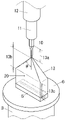
- FIG. 1 is a schematic cross-sectional view illustrating a growth furnace as an example of a method for producing a Ga 2 O 3 -based single crystal by the EFG method.
- FIG. FIG. 2 is an explanatory diagram of a method for producing a Ga 2 O 3 -based single crystal by the EFG method; 1 is a perspective view showing an example of a Ga 2 O 3 -based single crystal substrate according to an embodiment of the present invention;
- FIG. FIG. 2 is a perspective view showing another example of a Ga 2 O 3 -based single crystal substrate according to an embodiment of the present invention;
- FIG. 5 is an explanatory diagram showing measurement standards of SORI in the Ga 2 O 3 -based single crystal substrates of FIGS. 3 and 4.
- FIG. FIG. 6 is an explanatory diagram showing the measurement criteria of the BOW shown in FIG. 5; Structure of UV LED (Example 3). Structure of vertical MISFET (Example 4).
- the Ga 2 O 3 system is ⁇ -type Ga 2 O 3 or ⁇ -Ga 2 O 3 containing Al.
- it contains Al, it is a crystal having a composition ratio of (Al 1-x Ga x ) 2 O 3 (0 ⁇ X ⁇ 1).
- FIG. 1 is a schematic cross-sectional view showing the structure of a Ga 2 O 3 -based single crystal growth apparatus 1 using the EFG method.
- the crystal growth method is not limited to the EFG method, and may be the CZ (Czochralski) method, the Bridgman method, or the Flux method.
- a crucible 3 filled with a Ga 2 O 3 -based single crystal raw material and a die 5 provided with a slit 5A are installed in the crucible 3 inside the growth apparatus 1 .
- a lid 6 is placed on the upper surface of the crucible 3 except for the die 5 portion.
- the Ga 2 O 3 raw material to be used is Ga 2 O 3 having a high purity of 5N (99.999%) or higher, preferably 6N (99.9999%) or higher, and having a high bulk density.
- various additives are added to the raw material. good too.
- an n-type dopant one or more elements of group 14 and group 17 elements are introduced.
- a p-type dopant one or more elements of Groups 1, 2, and 15 and Fe, Cu, and Zn are introduced.
- a high-melting-point material that does not easily react with steam and has heat resistance above about 1800°C is used.
- iridium is the most suitable material, so iridium is used. Therefore, the growth atmosphere must be an inert atmosphere containing 100 vol.
- the crucible 3 may be pressurized to suppress evaporation of raw materials.
- the crucible 3 is induction-heated to a predetermined temperature by a heater section 9 consisting of an induction heating coil, the raw material in the crucible 3 is melted, and the melt rises through the slit 5A due to capillary action.
- a heating method for crystal growth there is resistance heating, which is generally used for growing Si single crystals by the CZ method, but induction heating is more suitable for growing Ga 2 O 3 single crystals.
- induction heating is more suitable for growing Ga 2 O 3 single crystals.
- Ga 2 O 3 is highly susceptible to sublimation and evaporation at high temperatures. Since sublimation and decomposition/evaporation occur from the grown crystals, those crystals become thin and thin, and in the worst case, all the crystals sublimate, decompose/evaporate, and disappear. As a result, the yield of crystal growth is lowered, or the crystal cannot be grown.
- the seed crystal 10 is lowered above the slit 5A so that it partially contacts the die upper surface 5B where the melt 2 is exposed. After that, by pulling the seed crystal 10 at a predetermined speed, crystallization is started from the melt contact portion of the seed crystal 10 .
- the direction of pulling is the direction of crystal growth.
- the temperature is raised as high as possible, and the seed crystal 10 is pulled up while adjusting the pulling speed to form a thin neck for removing dislocations in the crystal (necking 13a).
- the growth temperature is set to 1800° C. or higher, and the thickness of the neck portion is set to about half or less of the cross-sectional area of the seed crystal 10 in contact with the die upper surface portion 5B.
- the seed crystal preferably has as few dislocations as possible in order to obtain a single crystal with few dislocations.
- the rising speed of the seed crystal holder 11 is set to a predetermined speed, and the growth temperature is lowered at a predetermined rate so that the Ga 2 O 3 system single crystal 13 is spread over the width of the die 5 around the seed crystal 10 .
- the crystal is grown so as to widen at a constant angle ⁇ in the direction (spreading 13b).
- ⁇ ° is increased, atoms in the melt are rapidly aligned and crystallized, resulting in more twin crystals. Specifically, when the angle is set to 30° or less, twin crystals disappear and a single crystal with high crystallinity can be grown.
- the impurity concentration in the single crystal is 0.02 mol % or more, twin crystals do not occur regardless of the magnitude of ⁇ . Twin crystals occur when the impurity concentration is lower than 0.02 mol %. Note that when the impurity concentration is higher than 0.15 mol %, the crystallinity deteriorates although twin crystals do not occur. Therefore, the impurity concentration is preferably 0.15 mol % or less.
- the portion (straight body portion 13c) having the same width shape as the full width of the die 5 is pulled up to an appropriate length.
- the substrate is pulled up by about 55 mm at 10 mm/hr.
- the dislocation density of the Ga 2 O 3 system single crystal 13 can be reduced to 1.0 ⁇ 10 5 /cm 2 or less by necking, spreading and growing the straight body portion.
- the pulling plane orientation can be set in various ways according to the plane orientation of the main surface.
- the pulling direction should be 7° or less with respect to any one of the a-axis, b-axis, and c-axis where crystallization is easy during crystal growth and cracks, peeling, and chipping are less likely to occur during substrate processing. Pull up in any direction inclined within the range of .
- the main surface 15 of the substrate 16 or 21 is the (100) plane, which enables formation of a high-quality semiconductor layer with good surface morphology on the main surface 15 and is suitable for fabricating device structures such as ultraviolet LEDs.
- a method for processing the grown Ga 2 O 3 system single crystal 13 into a circular Ga 2 O 3 system single crystal substrate 16 as shown in FIG. 3 or a square shape 21 as shown in FIG. 4 will be described.
- a slicing machine, a core drill, an ultrasonic processing machine, or the like is used to cut out a circular or rectangular shape to produce a circular or rectangular substrate of a predetermined size.
- the end face of the substrate is shaped using an end face grinder.
- orientation flats may be formed on the substrate 16 or 21 as necessary.
- the main surface is the (100) plane or a surface inclined in the range of 7° or less from the (100) plane, it is perpendicular to the main surface and parallel to the b axis or 5° from the b axis is provided as an orientation flat.
- the above principal plane is other than the (100) plane or a plane inclined in the range of 7° or less from the (100) plane, the An end face is provided in a direction parallel to or inclined within a range of 5° from the parallel direction.
- One or more orientation flats may be provided on the main surface as shown in FIG. 3(b).
- one or more corner cutouts may be provided by using the end face of the corner cutout portion as an orientation flat as shown in FIG. 4(b).
- one side of the manufactured substrate 16 or 21 is used as the main surface 15, and the main surface 15 is subjected to polishing processing such as lapping and polishing to make the main surface 15 super flat. Further, the rear surface 19 is also subjected to polishing according to necessity such as shape, and at the same time the thickness of the substrate 16 or 21 is adjusted.
- Abrasive grains for lapping use silicon carbide or alumina. Chemical mechanical polishing is used for polishing, and colloidal silica is used for CMP abrasive grains.
- the surface roughness Ra of the main surface 15 is 3.0 nm or less, and the surface roughness Ra of the back surface 19 is 0.1 nm or more as required.
- the purpose is to remove residual thermal strain, residual processing strain, and coloring, which are common to those skilled in the field of substrate processing such as Si, GaAs, and sapphire single crystal, and to improve electrical characteristics.
- a heat treatment for the purpose is carried out as appropriate.
- the atmosphere gas for heat treatment may be nitrogen, carbon dioxide, argon, oxygen, or air, excluding a reducing gas such as hydrogen gas, which has the effect of roughening the substrate surface, and may be appropriately combined.
- the treatment temperature is 500-1600°C, preferably 700-1400°C. Also, it may be pressurized.
- the shape of the substrate in the plane direction is rectangular, circular, or rectangular or circular with an orientation flat.
- the long side is 15 mm from the viewpoint that it is possible to secure the rigidity as, and it has the strength to the extent that it does not cause any inconvenience in handling, and it is possible to prevent cracks, peeling, and chipping.
- 150 mm or less is preferable, and in the case of each circular shape, the diameter is preferably ⁇ 25 mm or more and ⁇ 160 mm or less.
- the thickness of the substrate is preferably 0.10 mm or more and 2.0 mm or less.
- the amount of warpage of the main surface 15 is within the above range due to substrate processing including heat treatment of the substrate 16 or 21 and substrate cleaning.
- the substrate may be subjected to an internal modification process using a laser to achieve the above-described amount of warp.
- the amount of warpage is defined as having an absolute value of SORI (conforming to SEMI standards) and having a ⁇ sign that indicates the direction of warpage.
- the sign of ⁇ can be obtained from the cross-sectional view of the SORI measurement result, BOW measurement, etc.
- the board surface center position is above the reference plane, it is + (convex shape), and when it is below the reference plane, it is - (concave shape). shape).
- the above SORI and BOW are obtained using a flatness measuring device.
- an optical interference measuring device manufactured by NIDEK is used. The measurement is as follows.
- SORI is the maximum distance from the reference plane S on the front surface of the substrate 16 or 21 when the back surface of the substrate 16 or 21 is fixed by suction at one or three points (non-suction) with a suction chuck (not shown). It is the sum of the vertical distances (absolute values) between the point and the lowest point. Since the SORI is the sum of the absolute values of the vertical distances to the highest point and the lowest point, the SORI is always a positive value. Letting A be the vertical distance from the reference plane S to the highest point, and B be the vertical distance from the reference plane S to the lowest point, SORI is defined by Equation 1 below.
- the amount of warpage is -(
- the SORI value is the same as the so-called PV (Peak to Valley) value when the least-squares plane on the main surface 15 is used as the reference plane.
- BOW as shown in FIG. 6, is the point with the maximum absolute value and the opposite sign from the center C of the substrate on the front surface when the back surface of the substrate 16 is adsorbed at one to three points (non-adhered state). (excluding the center C) and the distance from the center C, as shown in FIG. Note that the upper side of the reference plane S is the positive side, and the lower side is the negative side. In FIG. 6, the center C is positioned below the reference plane S, so BOW has a negative value.
- the dislocation density of the substrate 16 or 21 cut from the single crystal grown by the EFG method is 1.0 ⁇ 10 5 /cm 2 or less.
- the dislocation density is measured with a transmission electron microscope (TEM). Also, since the dot-like etch pit density when the substrate is etched corresponds to the dislocation density, etching may be performed for evaluation.
- TEM transmission electron microscope
- the lamination method is not limited to the MOCVD method, such as the Molecular Beam Epitaxy (MBE) method, the Pulse Laser Deposition (PLD) method, and the Hydride Vapor Phase Epitaxy (HVPE) method.
- MBE Molecular Beam Epitaxy
- PLD Pulse Laser Deposition
- HVPE Hydride Vapor Phase Epitaxy
- an Al x Ga (1-x) N semiconductor layer is grown on the buffer layer at, eg, 800 to 1100° C. to a thickness of 100 ⁇ m or less, and the temperature is lowered after the growth is completed.
- the Ga 2 O 3 system single crystal substrate on which the Al x Ga (1-x) N system semiconductor is laminated is taken out, and quality evaluation of cracks and peeling is performed visually and using an optical microscope.
- Ga 2 O 3 -based epitaxial layer or an AlxGa(1-x)N-based epitaxial layer is once laminated on the entire surface or at least the main surface 15 of the substrates 16 and 21 by MOCVD, HVPE, or the like. good.
- MOCVD MOCVD
- HVPE HVPE
- laminating Ga 2 O 3 based epitaxial layers by laminating 50 ⁇ m or less on the main surface 15 , crystal defects are reduced and the surface roughness Ra of the main surface 15 becomes even smaller than the Ra value.
- a higher-quality Al x Ga (1-x) N layer can be laminated on the upper Ga 2 O 3 -based epitaxial layer.
- AlxGa(1-x)N system epitaxial layer lamination of 1 nm or more improves the resistance of the Ga 2 O 3 system single crystal substrate against hydrogen carrier gas, which is essential for normal nitride semiconductor growth. , the deterioration of the substrate can be suppressed. Therefore, a desired high-quality AlxGa (1-x) N -based semiconductor layer can be grown on a Ga2O3 - based single crystal substrate. Then, not only the Al x Ga (1-x) N-based semiconductor layer but also the Al x Ga (1-x) N-based semiconductor laminate including the substrates 16 and 21 can be obtained with high quality.
- the surfaces of the substrates 16 and 21 may be nitrided instead of the Al x Ga (1-x) N epitaxial layer.
- Ga 2 O 3 -based single crystal substrates according to samples 1 to 7 of the present example were formed by cutting out with a core drill from single crystals grown by b-axis pulling by the EFG method. Common conditions for each of the samples 1 to 7 are as follows. The shape of the substrate in the plane direction is circular with one orientation flat as shown in FIG . and contains 0.05mol%. Furthermore, the Ga 2 O 3 -based single crystal substrate had a diameter of 2 inches, a principal plane of (101) plane with an off angle of 0.0°, a thickness of 0.70 mm, and a dislocation density of 4 ⁇ 10 4 /cm 2 of the principal plane. Free.
- the outer shape of the substrate was shaped using a surface grinder. Then, the back surface of the substrate was subjected to lapping only, or lapping and polishing in the same manner as the main surface. Then, the main surface of the substrate was subjected to lapping and polishing. After polishing, organic cleaning, hydrofluoric acid cleaning, and RCA cleaning were performed.
- the amount of warpage of the Ga 2 O 3 single crystal substrate of each example sample was formed as shown in Table 1.
- Comparative example 1 As comparative samples 1 and 2, Ga 2 O 3 system single crystal substrates were processed in the same manner as in Example 1, and formed as shown in Table 2.
- An AlN buffer layer of 3 nm was grown at 550° C. on the main surface of each of the Ga 2 O 3 -based single crystal substrates of Example Samples 1 to 7 and Comparative Example Samples 1 and 2 by the MOCVD method, and then Si-doped n-type Al 0 was grown.
- a crystal of .4Ga0.6N composition was grown at 1050°C to 4um. After that, the temperature was lowered and the sample was taken out from the apparatus after reaching normal temperature.
- X-ray diffraction (XRD) measurement of the Al0.4Ga0.6N film showed that the entire main surface of each sample was the (0001) plane and was epitaxially grown. As a result of the quality evaluation, it was confirmed that neither the Al0.4Ga0.6N layer nor the Ga 2 O 3 system single crystal substrate in Examples 1 to 7 had cracks or peeling.
- Ga 2 O 3 -based single crystal substrates according to Example Samples 8 to 14 were formed by cutting out rectangular single crystals of 20 mm ⁇ 30 mm using a slicing machine from single crystals grown by pulling along the b-axis by the EFG method. Common conditions for each of the samples 8 to 14 are as follows. All of the substrates are rectangular in shape in the planar direction, and the Ga 2 O 3 -based single crystal forming the substrate is a ⁇ -Ga 2 O 3 single crystal, which is doped with 0.05 mol % of Si.
- the main surface of the Ga 2 O 3 single crystal substrate is the (101) plane with an off angle of 0.0°, the thickness is 0.70 mm, the dislocation density of the main surface is 4 ⁇ 10 4 /cm 2 , and the substrate is twin-free.
- Example 1 In the same manner as in Example 1, an AlN buffer layer and then an n-type Al 0.4 Ga 0.6 N composition were formed on the main surface of each of the Ga 2 O 3 -based single crystal substrates of Example Samples 8 to 14 and Comparative Example Samples 3 and 4. A crystal was grown and a sample was taken out after the temperature was lowered. From the X-ray diffraction (XRD) measurement of the Al 0.4 Ga 0.6 N film, it was confirmed that the main surface of all the samples was the (0001) plane and was epitaxially grown. As a result of the quality evaluation, it was confirmed that neither the Al 0.4 Ga 0.6 N layer nor the Ga 2 O 3 system single crystal substrate had cracks or peeling in Examples 8 to 14.
- XRD X-ray diffraction
- Example 3 Among the samples of Example 1, a vertical ultraviolet LED as an optical device was produced by duplicating a sample under the same conditions as Sample 4 in which cracks and peeling did not occur.
- FIG. 1 An example of the laminated structure of the vertical ultraviolet LED 23 is shown in FIG.
- an InAl 0.4 Ga 0.6 N layer 26 which is a Si-doped n-type cladding layer, is grown at 1000° C. to a thickness of 25 nm by MOCVD.
- In is added to improve the luminous efficiency, and its composition ratio is less than 1%.
- the InAl 0.5 Ga 0.5 N barrier layer 27 is set to 6 nm at 1050° C.
- the InAl 0.3 Ga 0.7 N quantum well layer 28 is set to 2 nm at 1050° C.
- the barrier layer and the quantum well layer are separated.
- a multilayer structure grown alternately is grown in three layers as shown in FIG.
- a Mg-doped p-type InAl 0.6 Ga 0.4 N electron blocking layer 29 is grown at 1050° C. to a thickness of 20 nm.
- a Mg-doped p-type InAl 0.5 Ga 0.5 N clad layer 30 is grown at 1050° C. to a thickness of 20 nm.
- a Mg-doped p-type InAl 0.3 Ga 0.7 N contact layer 31 is grown at 1000° C. to a thickness of 10 nm.
- a Ni/Al laminated structure that provides ohmic contact and highly reflects ultraviolet light coming from the light-emitting layer is formed on the p-type contact layer 31.
- n-side electrode 33 As the n-side electrode 33, a Ti/Au laminated structure is formed which is in ohmic contact with the Ga 2 O 3 system single crystal substrate 16 and highly transmits ultraviolet light coming from the light emitting layer side.
- this ultraviolet LED 23 By energizing the n-side electrode 33 and the p-side electrode 32, this ultraviolet LED 23 emitted ultraviolet light from the n-side electrode 33 side.
- the vertical ultraviolet LED 23 which could not be realized on the sapphire substrate, is realized with high quality without causing cracks or peeling. We were able to. Furthermore, since it became possible to produce vertical ultraviolet LEDs 23 on a large-sized substrate, it was possible to improve productivity.
- Example 4 Among the samples of Example 1, the one under the same conditions as Sample 5 in which no cracks or peeling occurred was duplicated, and a vertical metal-insulator-semiconductor field effect transistor (MISFET: Metal-Insulator-Semiconductor), which is a device for high withstand voltage power, was reproduced. field effect transistor).
- MISFET Metal-insulator-semiconductor field effect transistor
- N is ion-implanted into the n-type Al 0.4 Ga 0.6 N layer 25 using an ion implantation apparatus to form the p-type region 35 .
- a source electrode 37 having a Ti/Al laminated structure is formed on the p-type region 35 and the n+ region 36 by a vapor deposition apparatus as shown in FIG. Al2O3, which is a gate insulator 38, is formed on the n-Al 0.4 Ga 0.6 N layer 25, the p-type region 35, and the n + -type region 36 by a vapor deposition apparatus, and a gate electrode is formed on the gate insulator 38.
- Form 39 with Al is shown in FIG. Al2O3, which is a gate insulator 38, is formed on the n-Al 0.4 Ga 0.6 N layer 25, the p-type region 35, and the n + -type region 36 by a vapor deposition apparatus, and a gate electrode is formed on the gate insulator 38.
- the drain electrode 40 is formed with a Ti/Al laminated structure on the Ga 2 O 3 system single crystal side to complete the process.
- the high breakdown voltage vertical MISFET 34 in which the Al (1-x) Ga x N semiconductors are laminated can be prevented from cracking or cracking. It can be manufactured without peeling. Furthermore, the vertical MISFET 34 can be manufactured on a large-sized substrate, and productivity can be improved.
Abstract
[Problem] To realize a Ga2O3-based single crystal substrate with which it is possible to obtain a high quality and homogeneous semiconductor film without cracking or peeling occurring in the semiconductor layer or the Ga2O3-based single crystal substrate, even if an AlxGa(1-x)N (0 ≤ x ≤ 1)-based semiconductor is layered on the Ga2O3-based single crystal substrate; to provide a method for manufacturing the Ga2O3-based single crystal substrate; and to provide an AlxGa(1-x)N-based optical semiconductor device and an AlxGa(1-x)N-based power semiconductor device using the Ga2O3-based single crystal substrate. [Solution] Provided is a Ga2O3-based single crystal substrate in which the warpage amount of the main surface is -50 μm to 50 μm (including 0 μm). Provided is a method for manufacturing a Ga2O3-based single crystal substrate which is processed into a substrate from a Ga2O3-based single crystal grown through an induction heating type single crystal growing method, the warpage amount of the main surface being -50 μm to 50 μm (including 0 μm).
Description
本発明は、Ga2O3系単結晶基板並びにGa2O3系単結晶基板の製造方法に関する。
The present invention relates to a Ga 2 O 3 -based single crystal substrate and a method for producing a Ga 2 O 3 -based single crystal substrate.
従来、酸化ガリウム(Ga2O3)系単結晶基板上にAlxGa(1-x)N(0≦x≦1)系半導体を積層して発光ダイオード(LED:Light Emitting Diode)や電界効果トランジス(FET:Field Effect Transistor)等の各種電子デバイスを作る開発が試みられている(例えば特許文献1参照)。
Conventionally, Al x Ga (1-x) N (0 ≤ x ≤ 1) based semiconductors have been stacked on gallium oxide (Ga 2 O 3 ) based single crystal substrates to form light emitting diodes (LEDs) and field effect devices. Attempts have been made to develop various electronic devices such as transistors (FETs: Field Effect Transistors) (see Patent Document 1, for example).
特許文献1によれば、Ga2O3系単結晶基板上に、まず低温AlNバッファ層を積層することで、バッファ層上に窒化物半導体層等を積層していき、各種デバイス構造を作り込むことを可能としている。
According to Patent Document 1, a low-temperature AlN buffer layer is first laminated on a Ga 2 O 3 -based single crystal substrate, and then a nitride semiconductor layer or the like is laminated on the buffer layer to create various device structures. making it possible.
しかし、実際のところ、Ga2O3系単結晶基板上に低温AlNバッファ層、次にAlxGa(1-x)N系半導体層を積層した場合、熱膨張係数や格子定数がGa2O3系単結晶基板とAlxGa(1-x)N系半導体層とで異なるため、前記半導体積層時もしくは積層後常温に戻した際に、AlxGa(1-x)N系半導体層及びGa2O3系単結晶基板が反るとともに、前記半導体層や前記基板にクラックや剥離が発生し、高品質で均質なAlxGa(1-x)N系半導体層を積層できないことが多い。
However, in actuality, when a low-temperature AlN buffer layer and then an AlxGa (1-x) N - based semiconductor layer are stacked on a Ga2O3 - based single crystal substrate, the thermal expansion coefficient and lattice constant change to that of Ga2O3. Since the 3 -based single crystal substrate and the Al x Ga (1-x) N-based semiconductor layer are different, the Al x Ga (1-x) N-based semiconductor layer and the Al x Ga (1-x) N-based semiconductor layer and As the Ga 2 O 3 single crystal substrate warps, cracks and peeling occur in the semiconductor layer and the substrate, and it is often impossible to laminate a high-quality and homogeneous Al x Ga (1-x) N semiconductor layer. .
そのため、特許文献2によれば、低温AlNバッファ層上に界面抵抗低減層、次いで応力緩和層を積層し、前記応力緩和層上にAlxGa(1-x)N系半導体層を積層する方法にすることで、前記半導体層のクラックが効果的に抑えられたAlxGa(1-x)N系半導体が得られるとされる。
Therefore, according to Patent Document 2, a method of stacking an interfacial resistance reduction layer and then a stress relaxation layer on a low-temperature AlN buffer layer, and stacking an Al x Ga (1-x) N-based semiconductor layer on the stress relaxation layer. By doing so, an Al x Ga (1-x) N-based semiconductor in which cracks in the semiconductor layer are effectively suppressed can be obtained.
しかし、特許文献2に記載の方法でも、依然としてクラックや剥離は残存しており、不十分であった。また、界面抵抗低減層や応力緩和層という新たな半導体積層工程が増えることは、積層工程が複雑になることから望ましくない。
However, even with the method described in Patent Document 2, cracks and delamination still remain and are insufficient. Moreover, it is not desirable to add a new semiconductor lamination process for the interfacial resistance reduction layer and the stress relaxation layer because the lamination process becomes complicated.
現状のところ、Ga2O3系単結晶基板上への半導体の積層技術は研究開発途上にある。半導体積層技術においては、一般的に、単結晶の属する結晶系が何であるかが最も大事な基本要素の一つである。現在各種半導体デバイスに使われている主要な半導体単結晶基板は、例えばSi基板やGaAs基板、SiC(4H)基板、サファイア基板などがあるが、それらの結晶系はそれぞれ立方晶、立方晶、六方晶、三方晶であり、いずれも対称性の高い結晶系であり、また劈開性は弱い。それらに対し、新しい結晶であるGa2O3系単結晶は、対称性が低い珍しい結晶系である単斜晶に属するため、また極めて強い劈開性を示しクラックや剥離が非常に発生し易いため、これまでの半導体積層技術が通じない可能性があった。
At present, the technology for stacking semiconductors on Ga 2 O 3 -based single crystal substrates is under research and development. In semiconductor lamination technology, generally, the crystal system to which a single crystal belongs is one of the most important basic elements. Major semiconductor single crystal substrates currently used in various semiconductor devices include, for example, Si substrates, GaAs substrates, SiC(4H) substrates, and sapphire substrates.These crystal systems are cubic, cubic, and hexagonal, respectively. They are crystals and trigonal crystals, both of which are highly symmetrical crystal systems and have weak cleavage. On the other hand, the new Ga 2 O 3 system single crystal belongs to the monoclinic crystal system, which is a rare crystal system with low symmetry. , there was a possibility that conventional semiconductor lamination technology would not work.
本発明は上記課題に鑑みてなされたものであり、Ga2O3系単結晶基板上にAlxGa(1-x)N(0≦x≦1)系半導体を積層させても、当該半導体層やGa2O3系単結晶基板中にクラックや剥離が発生することがなく、高品質で均質な当該半導体膜が得られるGa2O3系単結晶基板の実現と、当該Ga2O3系単結晶基板の製造方法、及び当該Ga2O3系単結晶基板用いたAlxGa(1-x)N系光半導体デバイス並びにAlxGa(1-x)N系電力用半導体デバイスの提供を目的とする。
The present invention has been made in view of the above problems . Realization of a Ga 2 O 3 -based single crystal substrate that does not cause cracks or peeling in the layer or the Ga 2 O 3 -based single crystal substrate and provides a high-quality and homogeneous semiconductor film, and the Ga 2 O 3 -based single crystal substrate. A manufacturing method for a single crystal substrate, and an Al x Ga (1-x) N-based optical semiconductor device and an Al x Ga (1-x) N-based power semiconductor device using the Ga 2 O 3 -based single crystal substrate. With the goal.
上記課題は、本発明者が鋭意検討を重ねた結果、以下の〔1〕~〔18〕の本発明により解決されることを見出した。
As a result of extensive studies, the inventors of the present invention have found that the above problems can be solved by the following inventions [1] to [18].
〔1〕主面の反り量が-50μm以上50μm以下(0μmを含む)であるGa2O3系単結晶基板。
[1] A Ga 2 O 3 -based single crystal substrate having a principal surface with a warp amount of −50 μm or more and 50 μm or less (including 0 μm).
〔2〕平面形状が円形状であり、円形状の直径が24mm以上160mm以下で、厚みが0.1mm以上2.0mm以下である上記〔1〕に記載のGa2O3系単結晶基板。
[2] The Ga 2 O 3 -based single crystal substrate according to [1] above, which has a circular planar shape, a diameter of 24 mm or more and 160 mm or less, and a thickness of 0.1 mm or more and 2.0 mm or less.
〔3〕平面形状が方形状であり、方形状の長辺が15mm以上150mm以下で、厚みが0.1mm以上2.0mm以下である上記〔1〕に記載のGa2O3系単結晶基板。
[3] The Ga 2 O 3 -based single crystal substrate according to [1] above, which has a square planar shape, a long side of 15 mm or more and 150 mm or less, and a thickness of 0.1 mm or more and 2.0 mm or less.
〔4〕上記方形状が正方形で、少なくとも一つ以上の角が欠けている上記〔3〕に記載のGa2O3系単結晶基板。
[4] The Ga 2 O 3 -based single crystal substrate according to [3] above, wherein the rectangular shape is a square and lacks at least one corner.
〔5〕上記主面が(100)面、(010)面、(001)面、(-201)面、(101)面の何れかである上記〔1〕~〔4〕の何れかに記載のGa2O3系単結晶基板。
[5] Any one of [1] to [4] above, wherein the principal plane is any one of (100) plane, (010) plane, (001) plane, (-201) plane and (101) plane. Ga 2 O 3 single crystal substrate.
〔6〕(100)面、(010)面、(001)面、(-201)面、(101)面の何れかに対して、7°以下の範囲で傾斜した面(但し、0°は含まない)が、上記主面である上記〔1〕~〔4〕の何れかに記載のGa2O3系単結晶基板。
[6] A plane inclined in the range of 7° or less with respect to any of the (100) plane, (010) plane, (001) plane, (-201) plane, and (101) plane (however, 0° not included) is the main surface of the Ga 2 O 3 system single crystal substrate according to any one of [1] to [4] above.
〔7〕上記主面が、(100)面もしくは(100)面から7°以下の範囲で傾斜した面で、上記主面に垂直でありかつb軸に対して平行又は5°の範囲内で傾斜した端面が、少なくとも1つ設けられている上記〔1〕~〔6〕 の何れかに記載のGa2O3系単結晶基板。
[7] The principal plane is the (100) plane or a plane inclined by 7° or less from the (100) plane, perpendicular to the principal plane and parallel to the b-axis or within a range of 5°. The Ga 2 O 3 -based single crystal substrate according to any one of [1] to [6] above, wherein at least one inclined end surface is provided.
〔8〕上記主面が(100)面以外もしくは(100)面以外の面から7°以下の範囲で傾斜した面以外であり、上記主面に垂直でありかつ上記主面と(100)面との交線に対し平行又は平行方向から5°の範囲内で傾斜した端面が、少なくとも1つ設けられている上記〔1〕~〔6〕 の何れかに記載のGa2O3系単結晶基板。
[8] The main surface is other than the (100) plane or a plane inclined in the range of 7° or less from a plane other than the (100) plane, is perpendicular to the above main surface, and is both the main surface and the (100) plane. The Ga 2 O 3 single crystal according to any one of the above [1] to [6], which has at least one end face that is parallel to or inclined within the range of 5° from a direction parallel to the line of intersection with substrate.
〔9〕上記主面の転位密度が0個/cm2以上1×105個/cm2以下である上記〔1〕~〔8〕の何れかに記載のGa2O3系単結晶基板。
[9] The Ga 2 O 3 -based single crystal substrate according to any one of [1] to [8] above, wherein the main surface has a dislocation density of 0/cm 2 or more and 1×10 5 /cm 2 or less.
〔10〕n型ドーパントである第14族元素又は第17族元素の1つ以上の元素を、計0.02mol%以上0.15 mol%以下の範囲で含有する上記〔1〕~〔9〕の何れかに記載のGa2O3系単結晶基板。
[10] Any of the above [1] to [9] containing one or more elements of Group 14 elements or Group 17 elements, which are n-type dopants, in a total range of 0.02 mol% or more and 0.15 mol% or less. 3. The Ga 2 O 3 -based single crystal substrate according to .
〔11〕p型ドーパントである第1族元素、第2族元素、第15族元素、又はFe、Cu、Znの1つ以上の元素を、計0.02mol%以上0.15 mol%以下の範囲で含有する上記〔1〕~〔9〕の何れかに記載のGa2O3系単結晶基板。
[11] Contains a p-type dopant, Group 1 element, Group 2 element, Group 15 element, or one or more elements of Fe, Cu, and Zn, in a total range of 0.02 mol% or more and 0.15 mol% or less. The Ga 2 O 3 -based single crystal substrate according to any one of [1] to [9] above.
〔12〕上記主面上にAlxGa(1-x)N(0≦X≦1)系半導体層が形成されている上記〔1〕~〔11〕の何れかに記載のGa2O3系単結晶基板。
[12] Ga 2 O 3 according to any one of [1] to [11] above, wherein an Al x Ga (1-x) N (0≤X≤1) based semiconductor layer is formed on the main surface. system single crystal substrate.
〔13〕上記主面上に、Ga2O3系エピタキシャル層又はAlGaN系エピタキシャル層が、積層形成されている上記〔1〕~〔11〕の何れかに記載のGa2O3系単結晶基板。
[13] The Ga 2 O 3 system single crystal substrate according to any one of the above [1] to [11], wherein a Ga 2 O 3 system epitaxial layer or an AlGaN system epitaxial layer is laminated on the main surface. .
〔14〕上記Ga2O3系エピタキシャル層又は上記AlGaN系エピタキシャル層の厚みが、1nm以上50μm以下である上記〔13〕に記載のGa2O3系単結晶基板。
[14] The Ga2O3 - based single crystal substrate according to [13] above, wherein the Ga2O3 - based epitaxial layer or the AlGaN-based epitaxial layer has a thickness of 1 nm or more and 50 µm or less.
〔15〕上記Ga2O3系エピタキシャル層、又は上記AlGaN系エピタキシャル層の表面粗さRaが、3nm以下である上記〔13〕又は〔14〕に記載のGa2O3系単結晶基板。
[15] The Ga2O3 - based single crystal substrate according to [13] or [14] above, wherein the Ga2O3 - based epitaxial layer or the AlGaN-based epitaxial layer has a surface roughness Ra of 3 nm or less.
〔16〕誘導加熱方式の単結晶育成方法によって育成されるGa2O3系単結晶から基板加工されて、主面の反り量が-50μm以上50μm以下(0μmを含む)になるGa2O3系単結晶基板の製造方法。
[16] A Ga 2 O 3 substrate processed from a Ga 2 O 3 -based single crystal grown by an induction heating single crystal growth method, and having a principal surface warp amount of −50 μm or more and 50 μm or less (including 0 μm). A method for producing a single crystal substrate.
〔17〕上記Ga2O3系単結晶を育成する方向が、a軸,b軸,c軸方向の何れか、又はa軸,b軸,c軸方向の何れかの方向に対して7°以下の範囲で傾斜した方向(但し、0°は含まない)である上記〔16〕に記載のGa2O3系単結晶基板の製造方法。
[17] The direction in which the Ga 2 O 3 single crystal is grown is 7° to any one of the a-axis, b-axis, and c-axis directions, or any one of the a-axis, b-axis, and c-axis directions. The method for producing a Ga 2 O 3 -based single crystal substrate according to the above [16], wherein the direction is inclined within the following range (excluding 0°).
〔18〕上記Ga2O3系単結晶基板の全表面のうち、少なくとも主面上に、Ga2O3系エピタキシャル層又はAlGaN系エピタキシャル層を形成する上記〔16〕又は〔17〕に記載のGa2O3系単結晶基板の製造方法。
[18] The above [16] or [17], wherein a Ga 2 O 3 -based epitaxial layer or an AlGaN-based epitaxial layer is formed on at least the main surface of the entire surface of the Ga 2 O 3 -based single crystal substrate. A method for producing a Ga 2 O 3 -based single crystal substrate.
本発明のGa2O3系単結晶基板を下地基板に用いると、AlxGa(1-x)N系半導体の積層段階に発生するクラックや剥離を無くすことができ、また積層時の反りを小さく抑えられることから基板面内温度分布を均一にできるため、高品質で均質なAlxGa(1-x)N系半導体積層膜を成長できることを見出した。そのため、例えば、光半導体デバイスの一種であるAlxGa(1-x)N系紫外LEDを高品質に作製できようになり、1枚の基板からより多くの紫外LED素子が得られるようになるためその歩留まりが上がる。更に大型化基板での紫外LED作製も可能となるため生産性が向上する。また、同様のことが電力用半導体デバイスにも適用できる。
When the Ga 2 O 3 single crystal substrate of the present invention is used as a base substrate, it is possible to eliminate cracks and peeling that occur during the lamination step of Al x Ga (1-x) N semiconductors, and to prevent warping during lamination. It was found that high-quality and uniform Al x Ga (1-x) N-based semiconductor laminated films can be grown because the temperature distribution in the substrate surface can be made uniform because the temperature can be kept small. As a result, for example, Al x Ga (1-x) N-based ultraviolet LEDs, which are a type of optical semiconductor device, can be manufactured with high quality, and more ultraviolet LED elements can be obtained from a single substrate. Therefore, the yield increases. Furthermore, it is possible to manufacture ultraviolet LEDs on large substrates, which improves productivity. Also, the same applies to power semiconductor devices.
本実施の形態において、Ga2O3系とは、β型Ga2O3、もしくはAlが含まれたβ-Ga2O3である。Alを含む場合は、組成比が(Al1-xGax)2O3(0<X≦1)である結晶である。
In the present embodiment, the Ga 2 O 3 system is β-type Ga 2 O 3 or β-Ga 2 O 3 containing Al. When it contains Al, it is a crystal having a composition ratio of (Al 1-x Ga x ) 2 O 3 (0<X≦1).
基板16又は21の切り出し元のGa2O3系単結晶の育成方法の一例として、EFG(Edge-defined Film-fed Growth)法が挙げられる。図1は、EFG法を用いたGa2O3系単結晶の育成装置1の構造を示す模式断面図である。なお、結晶育成方法は、EFG法に制限されず、CZ(Czochralski)法やブリッジマン(Bridgman)法、フラックス(Flux)法でもよい。
An example of a method for growing the Ga 2 O 3 -based single crystal from which the substrate 16 or 21 is cut is the EFG (Edge-defined Film-fed Growth) method. FIG. 1 is a schematic cross-sectional view showing the structure of a Ga 2 O 3 -based single crystal growth apparatus 1 using the EFG method. The crystal growth method is not limited to the EFG method, and may be the CZ (Czochralski) method, the Bridgman method, or the Flux method.
図1に示すように、育成装置1の内部には、Ga2O3系単結晶の原料を充填する坩堝3、そして、スリット5Aが設けられているダイ5が、坩堝3内に設置されている。坩堝3の上面には、ダイ5の部分を除いて蓋6がしてある。
As shown in FIG. 1, a crucible 3 filled with a Ga 2 O 3 -based single crystal raw material and a die 5 provided with a slit 5A are installed in the crucible 3 inside the growth apparatus 1 . there is A lid 6 is placed on the upper surface of the crucible 3 except for the die 5 portion.
ここで、使用するGa2O3原料は、純度5N(99.999%)以上、好ましくは6N(99.9999%)以上の高純度で、さらに高嵩密度になるGa2O3である。また、所望するGa2O3系単結晶基板の物性値(例えば、電気抵抗率、キャリアタイプ、キャリア密度、移動度、透過率、転位密度等)に応じて、原料に各種添加材を入れてもよい。例えば、n型ドーパントとして、14、17族元素のうち、1つ以上の元素を入れる。または、p型ドーパントとして、1、2、15族元素及びFe、Cu、Znのうち1つ以上の元素を入れる。
Here, the Ga 2 O 3 raw material to be used is Ga 2 O 3 having a high purity of 5N (99.999%) or higher, preferably 6N (99.9999%) or higher, and having a high bulk density. In addition, depending on the desired physical properties of the Ga 2 O 3 single crystal substrate (for example, electrical resistivity, carrier type, carrier density, mobility, transmittance, dislocation density, etc.), various additives are added to the raw material. good too. For example, as an n-type dopant, one or more elements of group 14 and group 17 elements are introduced. Alternatively, as a p-type dopant, one or more elements of Groups 1, 2, and 15 and Fe, Cu, and Zn are introduced.
β-Ga2O3の融点である約1800℃以上の高温になり、Ga2O3の融液や蒸気にさらされる坩堝3やダイ5、蓋6などは、Ga2O3の融液や蒸気と反応しにくく、かつ約1800℃超の耐熱性をもつ高融点材質のものが用いられる。現状、イリジウムが最も適しているためイリジウムを使う。そのため、育成雰囲気はアルゴンや窒素、二酸化炭素などの不活性ガス100Vol.%、もしくは酸素を10Vol.%程度まで含む不活性雰囲気である必要がある。坩堝3からの原料の蒸発を抑制するために加圧されていてもよい。
The crucible 3, the die 5, the lid 6, etc., which reach a high temperature of about 1800°C or higher, which is the melting point of β-Ga 2 O 3 , and are exposed to the Ga 2 O 3 melt or vapor, are exposed to the Ga 2 O 3 melt or vapor. A high-melting-point material that does not easily react with steam and has heat resistance above about 1800°C is used. Currently, iridium is the most suitable material, so iridium is used. Therefore, the growth atmosphere must be an inert atmosphere containing 100 vol. The crucible 3 may be pressurized to suppress evaporation of raw materials.
坩堝3は、誘導加熱コイルからなるヒータ部9により所定の温度に誘導加熱され、坩堝3内の原料が溶融し、融液が毛細管現象によりスリット5Aを上昇してくる。
The crucible 3 is induction-heated to a predetermined temperature by a heater section 9 consisting of an induction heating coil, the raw material in the crucible 3 is melted, and the melt rises through the slit 5A due to capillary action.
ここで、結晶育成における加熱方式には、一般的にSi単結晶のCZ法結晶育成で使われるような抵抗加熱もあるが、Ga2O3系単結晶育成の場合は誘導加熱のほうが適している。なぜなら、Ga2O3は高温で非常に昇華や蒸発が起き易い性質のため、ホットゾーン内全体の温度を高温に上げざるを得ない抵抗加熱での結晶育成の場合は、育成時、種結晶や育成した結晶から昇華や分解蒸発が発生するため、それらの結晶がやせて細くなり、最悪、結晶が全て昇華、分解蒸発し消失する。その結果、結晶育成の歩留まりが低下、ないしは結晶を育成できなくなる。それに対し、誘導加熱の場合は、坩堝3や蓋6などイリジウム部分だけが加熱され高温になる局所加熱のため、結晶は比較的冷えやすく、結晶部分からの昇華や分解蒸発はほぼ無視できる程度まで抑制される。また、誘導加熱の場合、無駄に加熱されることがないため坩堝3からの昇華や蒸発も比較的抑えられる。その結果、結晶育成の歩留まりや原料利用効率が向上する。さらに、加熱に要する消費電力量の低減も図れる。
Here, as a heating method for crystal growth, there is resistance heating, which is generally used for growing Si single crystals by the CZ method, but induction heating is more suitable for growing Ga 2 O 3 single crystals. there is This is because Ga 2 O 3 is highly susceptible to sublimation and evaporation at high temperatures. Since sublimation and decomposition/evaporation occur from the grown crystals, those crystals become thin and thin, and in the worst case, all the crystals sublimate, decompose/evaporate, and disappear. As a result, the yield of crystal growth is lowered, or the crystal cannot be grown. On the other hand, in the case of induction heating, only the iridium portion such as the crucible 3 and the lid 6 is heated locally to a high temperature, so the crystal is relatively easy to cool, and sublimation and decomposition evaporation from the crystal portion are almost negligible. Suppressed. In addition, in the case of induction heating, the sublimation and evaporation from the crucible 3 are relatively suppressed because the material is not heated wastefully. As a result, the yield of crystal growth and the utilization efficiency of raw materials are improved. Furthermore, the power consumption required for heating can be reduced.
まず、スリット5Aの上方にある種結晶10を下げていき、融液2が露出しているダイ上面部5Bに一部接触させる。その後、種結晶10を所定の速度で引き上げていくことで、種結晶10の融液接触部から結晶化が開始される。なお、引き上げ方向が結晶の育成方向となる。
First, the seed crystal 10 is lowered above the slit 5A so that it partially contacts the die upper surface 5B where the melt 2 is exposed. After that, by pulling the seed crystal 10 at a predetermined speed, crystallization is started from the melt contact portion of the seed crystal 10 . The direction of pulling is the direction of crystal growth.
できるだけ高温にして、引き上げ速度を調整しながら種結晶10を引き上げていき、結晶中の転位除去のため細いネック部を作る(ネッキング13a)。具体的には、育成温度1800℃以上で、ネック部太さを、種結晶10におけるダイ上面部5Bと接触する断面積の、約半分以下となるようにする。なお、結晶育成の原理上、転位が少ない単結晶を得るためには種結晶はできるだけ転位が少ないものが好ましい。
The temperature is raised as high as possible, and the seed crystal 10 is pulled up while adjusting the pulling speed to form a thin neck for removing dislocations in the crystal (necking 13a). Specifically, the growth temperature is set to 1800° C. or higher, and the thickness of the neck portion is set to about half or less of the cross-sectional area of the seed crystal 10 in contact with the die upper surface portion 5B. From the principle of crystal growth, the seed crystal preferably has as few dislocations as possible in order to obtain a single crystal with few dislocations.
次に、種結晶保持具11の上昇速度を所定の速度に設定し、また所定のレートで育成温度を下げていき、種結晶10を中心にGa2O3系単結晶13をダイ5の幅方向に一定角度θで拡幅する様に結晶育成させる(スプレディング13b)。双晶が無く、結晶性の高い単結晶を育成するためには、できるだけ育成温度変化を小さくし、θ°を小さくしてゆっくり広げることが好ましい。θ°を大きくすれば融液中の原子が急激に並び結晶化するため、双晶がより多く発生する。具体的には30°以下にすると双晶が無くなり結晶性の高い単結晶を育成できるようになる。
Next, the rising speed of the seed crystal holder 11 is set to a predetermined speed, and the growth temperature is lowered at a predetermined rate so that the Ga 2 O 3 system single crystal 13 is spread over the width of the die 5 around the seed crystal 10 . The crystal is grown so as to widen at a constant angle θ in the direction (spreading 13b). In order to grow a single crystal with no twins and high crystallinity, it is preferable to make the growth temperature change as small as possible, make θ° small, and spread slowly. If θ° is increased, atoms in the melt are rapidly aligned and crystallized, resulting in more twin crystals. Specifically, when the angle is set to 30° or less, twin crystals disappear and a single crystal with high crystallinity can be grown.
しかし、前記θの大小に関わらず、単結晶中の不純物濃度が0.02mol%以上の場合、双晶は発生しない。不純物濃度が0.02mol%より低いと双晶が発生する。なお、不純物濃度が0.15mol%より高い場合、双晶は発生しないものの、結晶性が悪くなる。そのため、不純物濃度は0.15mol%以下が好ましい。
However, if the impurity concentration in the single crystal is 0.02 mol % or more, twin crystals do not occur regardless of the magnitude of θ. Twin crystals occur when the impurity concentration is lower than 0.02 mol %. Note that when the impurity concentration is higher than 0.15 mol %, the crystallinity deteriorates although twin crystals do not occur. Therefore, the impurity concentration is preferably 0.15 mol % or less.
Ga2O3系単結晶13が、ダイ5の全幅まで広がると、続いて、ダイ5の全幅と同じ幅形状を有する部分(直胴部13c)を、適切な長さまで引き上げる。例えば、2インチ基板を作製する場合は、10mm/hrで、55mm程度引き上げる。上記のネッキング、スプレディングそして直胴部を育成することにより、Ga2O3系単結晶13の転位密度を1.0×105個/cm2以下に出来る。
After the Ga 2 O 3 -based single crystal 13 spreads over the full width of the die 5, the portion (straight body portion 13c) having the same width shape as the full width of the die 5 is pulled up to an appropriate length. For example, when manufacturing a 2-inch substrate, the substrate is pulled up by about 55 mm at 10 mm/hr. The dislocation density of the Ga 2 O 3 system single crystal 13 can be reduced to 1.0×10 5 /cm 2 or less by necking, spreading and growing the straight body portion.
引き上げ面方位は、主面の面方位に応じて種々設定可能である。引き上げ方向は、結晶育成の際に結晶化し易く、基板加工の際にクラックや剥離、チッピングが発生しにくくなるa軸、b軸、c軸の何れかの方向、又は各軸に対し7°以下の範囲で傾斜した何れかの方向で引き上げる。基板16又は21の主面15としては、高品質で良好な表面モフォロジーの半導体層を主面15上に形成する事が可能となり、紫外LED等のデバイス構造の作製に適した、(100)面、(010)面、(001)面、(101)面、(-201)面及び、(100)面、(010)面、(001)面、(101)面、(-201)面の何れかに対して7°以内の角度範囲(但し0°は含まない)で傾斜した面の何れかが好ましい。
The pulling plane orientation can be set in various ways according to the plane orientation of the main surface. The pulling direction should be 7° or less with respect to any one of the a-axis, b-axis, and c-axis where crystallization is easy during crystal growth and cracks, peeling, and chipping are less likely to occur during substrate processing. Pull up in any direction inclined within the range of . The main surface 15 of the substrate 16 or 21 is the (100) plane, which enables formation of a high-quality semiconductor layer with good surface morphology on the main surface 15 and is suitable for fabricating device structures such as ultraviolet LEDs. , (010) plane, (001) plane, (101) plane, (-201) plane and (100) plane, (010) plane, (001) plane, (101) plane, (-201) plane Any of the surfaces inclined within the angle range of 7° (but not including 0°) with respect to either is preferable.
次に、結晶育成されたGa2O3系単結晶13を図3のような円形状のGa2O3系単結晶基板16もしくは図4のような方形状21に基板加工する方法について説明する。例えば、スライシングマシンやコアドリル、超音波加工機等により、円形状又は方形状に切り抜き加工を施して、所定サイズの円形状基板又は方形状基板を作製する。
Next, a method for processing the grown Ga 2 O 3 system single crystal 13 into a circular Ga 2 O 3 system single crystal substrate 16 as shown in FIG. 3 or a square shape 21 as shown in FIG. 4 will be described. . For example, a slicing machine, a core drill, an ultrasonic processing machine, or the like is used to cut out a circular or rectangular shape to produce a circular or rectangular substrate of a predetermined size.
そして、端面研削盤を用いて基板端面の整形を行う。
Then, the end face of the substrate is shaped using an end face grinder.
また、上記切り抜き加工の前後において、必要に応じて、オリフラ(オリエンテーションフラット)を、基板16もしくは21に作製してもよい。
Before and after the cut-out process, orientation flats (orientation flats) may be formed on the substrate 16 or 21 as necessary.
上記オリフラについて、主面が(100)面ないしは(100)面から7°以下の範囲で傾斜した面の場合は、主面に垂直であり、かつb軸に対して平行又はb軸から5°の範囲内で傾斜した方向の端面をオリフラとして設けられている。上記主面が(100)面以外や(100)面から7°以下の範囲で傾斜した面以外の場合は、主面に垂直であり、かつ前記主面と(100)面との交線に対し平行又は平行になる方向から5°の範囲で傾斜した方向の端面が設けられている。
Regarding the orientation flat above, if the main surface is the (100) plane or a surface inclined in the range of 7° or less from the (100) plane, it is perpendicular to the main surface and parallel to the b axis or 5° from the b axis is provided as an orientation flat. If the above principal plane is other than the (100) plane or a plane inclined in the range of 7° or less from the (100) plane, the An end face is provided in a direction parallel to or inclined within a range of 5° from the parallel direction.
そして、上記オリフラは、図3(b)のように主面に対し、1つ以上設けられてもよい。
One or more orientation flats may be provided on the main surface as shown in FIG. 3(b).
なお、方形状基板が正方形である場合は、図4(b)のように角を欠けさせた部分の端面をオリフラとし、一つ以上角欠け部が設けられてもよい。
When the rectangular substrate is square, one or more corner cutouts may be provided by using the end face of the corner cutout portion as an orientation flat as shown in FIG. 4(b).
オリフラを上記結晶方位に作製することで、加工時において基板にクラックやチッピング、剥離が生じないようにすることができるとともに、基板の結晶方位を簡便に明示することができる。
By fabricating the orientation flat with the above crystal orientation, it is possible to prevent the substrate from cracking, chipping, and peeling during processing, and to easily indicate the crystal orientation of the substrate.
次いで、作製した基板16又は21の片面を主面15とし、その主面15に、ラッピング、ポリシングの研磨加工を施し、主面15を超平坦にする。また裏面19にも形状等の必要に応じた研磨加工を施し、同時に基板16又は21の厚みを調整する。ラッピングの砥粒は炭化ケイ素やアルミナを用いる。ポリシングは、化学機械研磨(Chemical Mechanical Polishing)を用い、CMP砥粒にはコロイダルシリカを用いる。
Next, one side of the manufactured substrate 16 or 21 is used as the main surface 15, and the main surface 15 is subjected to polishing processing such as lapping and polishing to make the main surface 15 super flat. Further, the rear surface 19 is also subjected to polishing according to necessity such as shape, and at the same time the thickness of the substrate 16 or 21 is adjusted. Abrasive grains for lapping use silicon carbide or alumina. Chemical mechanical polishing is used for polishing, and colloidal silica is used for CMP abrasive grains.
上記により、主面15の表面粗さRaは3.0nm以下となり、裏面19の表面粗さRaは必要に応じた粗さとなり、0.1nm以上となる。
Due to the above, the surface roughness Ra of the main surface 15 is 3.0 nm or less, and the surface roughness Ra of the back surface 19 is 0.1 nm or more as required.
上記研磨加工の終了後、基板に付着しているシリカ等の汚れを除去し、残留加工歪の除去調整や基板表面に清浄な酸化層を形成するため、アセトン等での有機洗浄後にフッ酸洗浄、さらにRCA洗浄を全てないしは一部を実施する。
After the above-mentioned polishing process is completed, contamination such as silica adhering to the substrate is removed, and in order to remove and adjust residual processing strain and to form a clean oxide layer on the substrate surface, organic cleaning with acetone etc. is followed by hydrofluoric acid cleaning. , and then perform all or part of the RCA cleaning.
さらに、上記基板加工工程において、SiやGaAs、サファイア単結晶等の基板加工分野の当業者にとっては一般的である、残留熱歪や残留加工歪、着色を除去する目的並びに電気的特性を改善する目的のための熱処理を、適宜実施する。熱処理の雰囲気ガスは、基板表面を荒らす効果がある水素ガスのような還元性ガスを除き、窒素、二酸化炭素、アルゴン、酸素、空気の何れかを使い、適宜組み合わせてもよい。処理温度は500℃~1600℃であり、好ましくは700~1400℃である。また、加圧されていてもよい。
Furthermore, in the substrate processing process, the purpose is to remove residual thermal strain, residual processing strain, and coloring, which are common to those skilled in the field of substrate processing such as Si, GaAs, and sapphire single crystal, and to improve electrical characteristics. A heat treatment for the purpose is carried out as appropriate. The atmosphere gas for heat treatment may be nitrogen, carbon dioxide, argon, oxygen, or air, excluding a reducing gas such as hydrogen gas, which has the effect of roughening the substrate surface, and may be appropriately combined. The treatment temperature is 500-1600°C, preferably 700-1400°C. Also, it may be pressurized.
なお、前記基板の平面方向の形状は、方形状、円形状、又はオリフラが設けられた方形状、円形状である。
The shape of the substrate in the plane direction is rectangular, circular, or rectangular or circular with an orientation flat.
そして、基板上にAlxGa(1-x)N系半導体膜を積層してもクラックや剥離が発生しないことはもちろんのこと、形状を精密にコントロールできるようにするため、また同時に自立した基板としての剛性が確保可能で、かつハンドリングに不都合が生じない程度の強度を有し、さらにクラックや剥離、チッピングの発生を防止可能であるとの観点から、前記方形状の場合は、長辺15mm以上150mm以下が好ましく、前記各円形状の場合は、直径φ25mm以上φ160mm以下が好ましい。
In addition to preventing cracks and delamination even when the Al x Ga (1-x) N semiconductor film is laminated on the substrate, we also developed a self-supporting substrate that allows for precise control of the shape. In the case of the above square shape, the long side is 15 mm from the viewpoint that it is possible to secure the rigidity as, and it has the strength to the extent that it does not cause any inconvenience in handling, and it is possible to prevent cracks, peeling, and chipping. 150 mm or less is preferable, and in the case of each circular shape, the diameter is preferably φ25 mm or more and φ160 mm or less.
上記同様の理由から、基板の厚みは0.10mm以上2.0mm以下が好ましい。
For the same reason as above, the thickness of the substrate is preferably 0.10 mm or more and 2.0 mm or less.
以上、基板16又は21の熱処理や基板洗浄を含む基板加工により、主面15の反り量は上記範囲内になる。なお、必要に応じて基板へのレーザーによる内部改質加工も施して上記反り量を実現してもよい。
As described above, the amount of warpage of the main surface 15 is within the above range due to substrate processing including heat treatment of the substrate 16 or 21 and substrate cleaning. In addition, if necessary, the substrate may be subjected to an internal modification process using a laser to achieve the above-described amount of warp.
ここで、反り量とは、その絶対値がSORI(SEMI規格準拠)の値であり、反りの方向を表す±の符号をもっていると定義する。±の符号は、SORI測定結果の断面図やBOW測定等から求められ、基板表面中心位置が基準平面より上の場合は+(凸型形状)、基準平面より下の場合は-である(凹型形状)。
Here, the amount of warpage is defined as having an absolute value of SORI (conforming to SEMI standards) and having a ± sign that indicates the direction of warpage. The sign of ± can be obtained from the cross-sectional view of the SORI measurement result, BOW measurement, etc. When the board surface center position is above the reference plane, it is + (convex shape), and when it is below the reference plane, it is - (concave shape). shape).
上記SORI、BOWは平面度測定装置を用いて求める。例えば光干渉方式の測定装置(NIDEK社製)を用いる。その測定については次の通りである。
The above SORI and BOW are obtained using a flatness measuring device. For example, an optical interference measuring device (manufactured by NIDEK) is used. The measurement is as follows.
まず、主面15上の全ての高さデータによる最小二乗平面が、基準平面Sとなる。
First, a least-squares plane based on all height data on the
SORIとは図5に示す様に、基板16又は21の裏面を吸着チャック(図示せず)により1点ないしは3点程度吸着固定した状態(非吸着)における、表面での基準平面Sからの最高点と最低点までの垂直距離(絶対値)の合計である。SORIは最高点及び最低点までの垂直距離が共に絶対値どうしでの足し算なので、SORIは常にプラスの値となる。基準平面Sから最高点までの垂直距離をA、基準平面Sから最低点までの垂直距離をBとすると、SORIは以下の数1で定義される。
As shown in FIG. 5, SORI is the maximum distance from the reference plane S on the front surface of the substrate 16 or 21 when the back surface of the substrate 16 or 21 is fixed by suction at one or three points (non-suction) with a suction chuck (not shown). It is the sum of the vertical distances (absolute values) between the point and the lowest point. Since the SORI is the sum of the absolute values of the vertical distances to the highest point and the lowest point, the SORI is always a positive value. Letting A be the vertical distance from the reference plane S to the highest point, and B be the vertical distance from the reference plane S to the lowest point, SORI is defined by Equation 1 below.
従って、例えば図5の場合は、反り量は-(|A|+|B|)である。
Therefore, in the case of FIG. 5, for example, the amount of warpage is -(|A|+|B|).
なお、SORI値は、主面15における最小二乗平面を基準面とした場合のいわゆるPV(Peak to Valley)値と同じである。
The SORI value is the same as the so-called PV (Peak to Valley) value when the least-squares plane on the main surface 15 is used as the reference plane.
BOWとは、図6に示す様に、基板16の裏面を1点ないし3点程度吸着させた状態(非吸着)における、表面での、基板中心Cとは異符号で絶対値が最大の点(中心Cを除く)と、中心Cとの距離を図6のように絶対値同士で和をとり中心Cの符号を付した値である。なお、基準平面Sより上側をプラス側、下側をマイナス側とする。図6では、中心Cは基準平面Sより下側に位置しているので、BOWはマイナスの値となる。
BOW, as shown in FIG. 6, is the point with the maximum absolute value and the opposite sign from the center C of the substrate on the front surface when the back surface of the substrate 16 is adsorbed at one to three points (non-adhered state). (excluding the center C) and the distance from the center C, as shown in FIG. Note that the upper side of the reference plane S is the positive side, and the lower side is the negative side. In FIG. 6, the center C is positioned below the reference plane S, so BOW has a negative value.
上記EFG法で育成した単結晶から切り出し基板加工した上記基板16又は21の転位密度は、1.0×10⁵個/cm2以下である。この様な低転位密度基板16又は21に半導体層を積層し、例えばLEDを作製すると、発光効率やデバイス寿命を高めることが出来る。また、例えば電力用デバイスに低転位密度基板16又は21を用いれば、電力変換効率やデバイス寿命を向上させることができる。
The dislocation density of the substrate 16 or 21 cut from the single crystal grown by the EFG method is 1.0×10 5 /cm 2 or less. By stacking semiconductor layers on such a low dislocation density substrate 16 or 21 to fabricate, for example, an LED, the luminous efficiency and device life can be improved. Further, if the low dislocation density substrate 16 or 21 is used for power devices, for example, power conversion efficiency and device life can be improved.
上記転位密度は、透過型電子顕微鏡(TEM:Transmission Electron Microscope)で測定する。また、基板をエッチングした場合における点状のエッチピット密度が転位密度に相当するため、エッチングして評価してもよい。
The dislocation density is measured with a transmission electron microscope (TEM). Also, since the dot-like etch pit density when the substrate is etched corresponds to the dislocation density, etching may be performed for evaluation.
次に、基板16又は21の主面15上への、半導体積層の一例として有機金属気相成長(MOCVD:Metal Organic Chemical Vapour Deposition)法による方法について説明する。なお、積層方法はMOCVD法に限られず、分子線エピタキシー(MBE:Molecular Beam Epitaxy)法やパルスレーザーデポジション(PLD:Pulse Laser Deposition)法、ハイドライド気相成長(HVPE:Hydride Vapour Phase Epitaxy)法などで成長させてもよい。結晶性の良好なAlxGa(1-x)N半導体積層膜が得られるようにするために、まずAlxGa(1-x)Nバッファ層を成長温度500~900℃で、厚さ1~200nm成長させる。
Next, a method using a metal organic chemical vapor deposition (MOCVD) method as an example of semiconductor lamination on the main surface 15 of the substrate 16 or 21 will be described. In addition, the lamination method is not limited to the MOCVD method, such as the Molecular Beam Epitaxy (MBE) method, the Pulse Laser Deposition (PLD) method, and the Hydride Vapor Phase Epitaxy (HVPE) method. You can grow it with In order to obtain an Al x Ga (1-x) N semiconductor laminated film with good crystallinity, first, an Al x Ga (1-x) N buffer layer was grown at a growth temperature of 500 to 900° C. to a thickness of 1 mm. Grow ~200nm.
次いで、上記バッファ層上にAlxGa(1-x)N半導体層を、例えば800~1100℃で、厚さ100um以下成長させ、成長終了後降温する。
Next, an Al x Ga (1-x) N semiconductor layer is grown on the buffer layer at, eg, 800 to 1100° C. to a thickness of 100 μm or less, and the temperature is lowered after the growth is completed.
常温付近に達した後、AlxGa(1-x)N系半導体が積層されたGa2O3系単結晶基板を取り出し、クラックや剥離の品質評価を、目視並びに光学顕微鏡を用いて行う。
After the temperature reaches around room temperature, the Ga 2 O 3 system single crystal substrate on which the Al x Ga (1-x) N system semiconductor is laminated is taken out, and quality evaluation of cracks and peeling is performed visually and using an optical microscope.
上記形態によれば、主面の反り量が前記上記範囲内のGa2O3系単結晶基板を下地基板に用いた場合、AlxGa(1-x)N系半導体の積層段階に発生するクラックや剥離を無くすことができる。また同時に積層時の反りを小さく抑えられることから基板面内温度分布を均一にできるため、高品質で均質なAlxGa(1-x)N系半導体積層を成長できる。
According to the above aspect, when a Ga 2 O 3 -based single crystal substrate having a main surface warp amount within the above-described range is used as a base substrate, warpage occurs during the lamination step of Al x Ga (1-x) N-based semiconductors. Cracks and delamination can be eliminated. At the same time, since the warp during lamination can be suppressed to a small level, the in-plane temperature distribution of the substrate can be made uniform, so that high-quality and homogeneous Al x Ga (1-x) N-based semiconductor lamination can be grown.
そのため、例えば光半導体デバイスの一種であるAlxGa(1-x)N系紫外LEDを高品質に作製できようになり、1枚の基板からより多くの紫外LED素子が得られるようになるため歩留まりが上がる。更に大型化基板での紫外LED作製も可能となるため生産性が向上する。また、同様のことが電力用半導体デバイスにも当てはまる。
Therefore, for example, it will be possible to manufacture high-quality Al x Ga (1-x) N-based ultraviolet LEDs, which are a type of optical semiconductor device, and it will be possible to obtain more ultraviolet LED elements from a single substrate. Yield increases. Furthermore, it is possible to manufacture ultraviolet LEDs on large substrates, which improves productivity. The same also applies to power semiconductor devices.
反対に、反り量が上記範囲外であるGa2O3系単結晶基板を下地基板に用いると、AlxGa(1-x)N系半導体の積層段階において、クラックや剥離が発生する。また積層時反りが大きくなり基板面内温度分布が不均一になるため、高品質で均質なAlxGa(1-x)N系半導体積層膜を成長することはできなくなる。
Conversely, if a Ga 2 O 3 -based single crystal substrate having a warpage amount outside the above range is used as the underlying substrate, cracks and peeling will occur in the lamination step of the Al x Ga (1-x) N -based semiconductor. In addition, since the warpage during lamination becomes large and the temperature distribution in the substrate surface becomes non-uniform, it becomes impossible to grow a high-quality and homogeneous Al x Ga (1-x) N-based semiconductor lamination film.
なお、基板16や21の、全表面ないしは少なくとも主面15上に、一旦Ga2O3系エピタキシャル層やAlxGa(1-x)N系エピタキシャル層をMOCVD法やHVPE法などにより積層形成してもよい。Ga2O3系エピタキシャル層を積層形成する場合、主面15上に50um以下積層する事で、結晶欠陥が低減され主面15の表面粗さRaよりも更にRa値が小さくなる。それにより、より高品質なAlxGa(1-x)N層を上Ga2O3系エピタキシャル層上に積層形成することが可能となる。AlxGa(1-x)N系エピタキシャル層の場合には、1nm以上積層することで、通常の窒化物系半導体成長に必須である水素キャリアガスに対するGa2O3系単結晶基板の耐性が向上し、基板の劣化が抑えられる。それゆえ所望の高品質なAlxGa(1-x)N系半導体層をGa2O3系単結晶基板上に成長することができる。そして、AlxGa(1-x)N系半導体層だけでなく、基板16や21を含めたAlxGa(1-x)N系半導体積層体としても高品質なものが得られる。
Even if a Ga 2 O 3 -based epitaxial layer or an AlxGa(1-x)N-based epitaxial layer is once laminated on the entire surface or at least the main surface 15 of the substrates 16 and 21 by MOCVD, HVPE, or the like. good. When laminating Ga 2 O 3 based epitaxial layers, by laminating 50 μm or less on the main surface 15 , crystal defects are reduced and the surface roughness Ra of the main surface 15 becomes even smaller than the Ra value. As a result, a higher-quality Al x Ga (1-x) N layer can be laminated on the upper Ga 2 O 3 -based epitaxial layer. In the case of the AlxGa(1-x)N system epitaxial layer, lamination of 1 nm or more improves the resistance of the Ga 2 O 3 system single crystal substrate against hydrogen carrier gas, which is essential for normal nitride semiconductor growth. , the deterioration of the substrate can be suppressed. Therefore, a desired high-quality AlxGa (1-x) N -based semiconductor layer can be grown on a Ga2O3 - based single crystal substrate. Then, not only the Al x Ga (1-x) N-based semiconductor layer but also the Al x Ga (1-x) N-based semiconductor laminate including the substrates 16 and 21 can be obtained with high quality.
さらに、上記AlxGa(1-x)N系エピタキシャル層の代わりに、基板16や21の表面を窒化処理しても良い。
Furthermore, the surfaces of the substrates 16 and 21 may be nitrided instead of the Al x Ga (1-x) N epitaxial layer.
以下に本発明に係る実施例を説明するが、本発明は以下の実施例にのみに限定されるものではない。
Examples according to the present invention will be described below, but the present invention is not limited only to the following examples.
(実施例1)
本実施例サンプル1~7に係るGa2O3系単結晶基板を、EFG法によりb軸引き上げで育成した単結晶からコアドリルによって切り抜き、形成した。各実施例サンプル1~7の共通条件は次の通りである。基板の平面方向の形状は、全て図3に示す1つのオリフラ面を設けた円形状であり、基板を形成するGa2O3系単結晶はβ-Ga2O3単結晶とし、Siがドープされ0.05mol%含有されている。更に、Ga2O3系単結晶基板の直径はφ2インチ、主面はオフ角が0.0°の(101)面、厚みは0.70mm、主面の転位密度は4x10⁴個/cm2で双晶フリーである。 (Example 1)
Ga 2 O 3 -based single crystal substrates according tosamples 1 to 7 of the present example were formed by cutting out with a core drill from single crystals grown by b-axis pulling by the EFG method. Common conditions for each of the samples 1 to 7 are as follows. The shape of the substrate in the plane direction is circular with one orientation flat as shown in FIG . and contains 0.05mol%. Furthermore, the Ga 2 O 3 -based single crystal substrate had a diameter of 2 inches, a principal plane of (101) plane with an off angle of 0.0°, a thickness of 0.70 mm, and a dislocation density of 4×10 4 /cm 2 of the principal plane. Free.
本実施例サンプル1~7に係るGa2O3系単結晶基板を、EFG法によりb軸引き上げで育成した単結晶からコアドリルによって切り抜き、形成した。各実施例サンプル1~7の共通条件は次の通りである。基板の平面方向の形状は、全て図3に示す1つのオリフラ面を設けた円形状であり、基板を形成するGa2O3系単結晶はβ-Ga2O3単結晶とし、Siがドープされ0.05mol%含有されている。更に、Ga2O3系単結晶基板の直径はφ2インチ、主面はオフ角が0.0°の(101)面、厚みは0.70mm、主面の転位密度は4x10⁴個/cm2で双晶フリーである。 (Example 1)
Ga 2 O 3 -based single crystal substrates according to
切り抜き後の基板に、熱処理を行った後、平面研削盤を用いて基板外形の整形を行った。そして、基板の裏面には、ラッピングのみ、もしくは主面と同様にラッピング及びポリッシングを施した。そして、基板の主面には、ラッピング及びポリッシングを施した。研磨終了後、有機洗浄、フッ酸洗浄、RCA洗浄を実施した。
After heat treatment was applied to the cut-out substrate, the outer shape of the substrate was shaped using a surface grinder. Then, the back surface of the substrate was subjected to lapping only, or lapping and polishing in the same manner as the main surface. Then, the main surface of the substrate was subjected to lapping and polishing. After polishing, organic cleaning, hydrofluoric acid cleaning, and RCA cleaning were performed.
実施例サンプル毎に主面及び裏面に施す加工の条件(研磨加工、熱処理、基板洗浄、内部改質加工)を変更する事で、各実施例サンプルのGa2O3系単結晶基板の反り量を表1の様に形成した。
By changing the processing conditions (polishing, heat treatment, substrate cleaning, internal modification processing) applied to the main surface and the back surface for each example sample, the amount of warpage of the Ga 2 O 3 single crystal substrate of each example sample was formed as shown in Table 1.

(比較例1)
また比較例サンプル1~2として、Ga2O3系単結晶基板の反り量を、実施例1と同様に加工し、表2の様に形成した。 (Comparative example 1)
As comparative samples 1 and 2, Ga 2 O 3 system single crystal substrates were processed in the same manner as in Example 1, and formed as shown in Table 2.
また比較例サンプル1~2として、Ga2O3系単結晶基板の反り量を、実施例1と同様に加工し、表2の様に形成した。 (Comparative example 1)
As

実施例サンプル1~7及び比較例サンプル1~2の各Ga2O3系単結晶基板の主面上にMOCVD法により、550℃でAlNバッファ層を3nm成長させ、次にSiドープn型Al0.4Ga0.6N組成の結晶を1050℃で4um成長させた。その後降温し、常温に到達後サンプルを装置から取り出した。Al0.4Ga0.6N膜のX線回折(XRD:X-Ray Diffraction)測定をすると、いずれのサンプルとも主面全面が(0001)面でありエピタキシャル成長していた。品質評価の結果、実施例1~7に於いては、Al0.4Ga0.6N層にも、Ga2O3系単結晶基板にも、クラックや剥離は発生していない事が確認された。
An AlN buffer layer of 3 nm was grown at 550° C. on the main surface of each of the Ga 2 O 3 -based single crystal substrates of Example Samples 1 to 7 and Comparative Example Samples 1 and 2 by the MOCVD method, and then Si-doped n-type Al 0 was grown. A crystal of .4Ga0.6N composition was grown at 1050℃ to 4um. After that, the temperature was lowered and the sample was taken out from the apparatus after reaching normal temperature. X-ray diffraction (XRD) measurement of the Al0.4Ga0.6N film showed that the entire main surface of each sample was the (0001) plane and was epitaxially grown. As a result of the quality evaluation, it was confirmed that neither the Al0.4Ga0.6N layer nor the Ga 2 O 3 system single crystal substrate in Examples 1 to 7 had cracks or peeling.
一方、全ての比較例サンプル1~2では、Al0.4Ga0.6N層やGa2O3系単結晶基板にクラックや剥離の何れかが発生している事が確認された。
On the other hand, in all comparative samples 1 and 2, it was confirmed that either cracks or peeling occurred in the Al 0.4 Ga 0.6 N layer or the Ga 2 O 3 system single crystal substrate.
(実施例2)
実施例サンプル8~14に係るGa2O3系単結晶基板を、EFG法によりb軸で引き上げて育成した単結晶からスライシングマシンによって20mm×30mmの長方形に切り抜き形成した。各実施例サンプル8~14の共通条件は次の通りである。基板の平面方向の形状は、全て長方形であり、基板を形成するGa2O3系単結晶はβ-Ga2O3単結晶とし、Siがドープされ0.05mol%含有されている。更に、Ga2O3系単結晶基板の主面はオフ角が0.0°の(101)面、厚みは0.70mm、主面の転位密度は4x10⁴個/cm2で双晶フリーである。 (Example 2)
Ga 2 O 3 -based single crystal substrates according toExample Samples 8 to 14 were formed by cutting out rectangular single crystals of 20 mm×30 mm using a slicing machine from single crystals grown by pulling along the b-axis by the EFG method. Common conditions for each of the samples 8 to 14 are as follows. All of the substrates are rectangular in shape in the planar direction, and the Ga 2 O 3 -based single crystal forming the substrate is a β-Ga 2 O 3 single crystal, which is doped with 0.05 mol % of Si. Further, the main surface of the Ga 2 O 3 single crystal substrate is the (101) plane with an off angle of 0.0°, the thickness is 0.70 mm, the dislocation density of the main surface is 4×10 4 /cm 2 , and the substrate is twin-free.
実施例サンプル8~14に係るGa2O3系単結晶基板を、EFG法によりb軸で引き上げて育成した単結晶からスライシングマシンによって20mm×30mmの長方形に切り抜き形成した。各実施例サンプル8~14の共通条件は次の通りである。基板の平面方向の形状は、全て長方形であり、基板を形成するGa2O3系単結晶はβ-Ga2O3単結晶とし、Siがドープされ0.05mol%含有されている。更に、Ga2O3系単結晶基板の主面はオフ角が0.0°の(101)面、厚みは0.70mm、主面の転位密度は4x10⁴個/cm2で双晶フリーである。 (Example 2)
Ga 2 O 3 -based single crystal substrates according to
そして、Ga2O3系単結晶基板の反り量を、実施例1と同様に加工して表3の様に形成した。
Then, the amount of warpage of the Ga 2 O 3 system single crystal substrate was processed in the same manner as in Example 1 and formed as shown in Table 3.

(比較例2)
また比較例サンプル3~4として、実施例2と同様に加工してGa2O3系単結晶基板の反り量を表4の様に形成した。 (Comparative example 2)
As Comparative Samples 3 and 4, the Ga 2 O 3 system single crystal substrates were processed in the same manner as in Example 2, and the amount of warp was formed as shown in Table 4.
また比較例サンプル3~4として、実施例2と同様に加工してGa2O3系単結晶基板の反り量を表4の様に形成した。 (Comparative example 2)
As

実施例サンプル8~14及び比較例サンプル3~4の各Ga2O3系単結晶基板の主面上に、実施例1と同様にしてAlNバッファ層、次いでn型Al0.4Ga0.6N組成の結晶を成長させ、降温後サンプルを取り出した。Al0.4Ga0.6N膜のX線回折(XRD)測定から、いずれのサンプルとも主面全面が(0001)面でありエピタキシャル成長していることが確認された。品質評価の結果、実施例8~14に於いては、Al0.4Ga0.6N層にも、Ga2O3系単結晶基板にも、クラックや剥離は発生していない事が確認された。
In the same manner as in Example 1, an AlN buffer layer and then an n-type Al 0.4 Ga 0.6 N composition were formed on the main surface of each of the Ga 2 O 3 -based single crystal substrates of Example Samples 8 to 14 and Comparative Example Samples 3 and 4. A crystal was grown and a sample was taken out after the temperature was lowered. From the X-ray diffraction (XRD) measurement of the Al 0.4 Ga 0.6 N film, it was confirmed that the main surface of all the samples was the (0001) plane and was epitaxially grown. As a result of the quality evaluation, it was confirmed that neither the Al 0.4 Ga 0.6 N layer nor the Ga 2 O 3 system single crystal substrate had cracks or peeling in Examples 8 to 14.
一方、全ての比較例サンプル3~4では、n型Al0.4Ga0.6N層やGa2O3系単結晶基板にクラックや剥離の何れかが発生している事が確認された。
On the other hand, in all comparative samples 3 and 4, it was confirmed that either cracks or peeling occurred in the n-type Al 0.4 Ga 0.6 N layer or the Ga 2 O 3 system single crystal substrate.
以上、実施例1、2及び比較例1、2から、反り量の範囲を-50μm以上+50μm以下に収めた基板16又は21を、Al(1-x)GaxN系半導体を積層する際に下地基板として用いた場合、クラックや剥離を無くすことができる。また同時に積層時の基板面内温度分布を均一にできることから、主面に高品質で均質なAl(1-x)GaxN系半導体積層膜を成長させることが可能になった。
As described above, from Examples 1 and 2 and Comparative Examples 1 and 2, when laminating Al When used as a base substrate, cracks and peeling can be eliminated. At the same time, since the temperature distribution within the substrate surface during lamination can be made uniform, it has become possible to grow a high-quality, homogeneous Al (1-x) Ga x N-based semiconductor lamination film on the main surface.
(実施例3)
実施例1サンプルのうち、クラックや剥離が発生していないサンプル4と同条件のものを複製し、光デバイスである縦型紫外LEDを作製した。 (Example 3)
Among the samples of Example 1, a vertical ultraviolet LED as an optical device was produced by duplicating a sample under the same conditions asSample 4 in which cracks and peeling did not occur.
実施例1サンプルのうち、クラックや剥離が発生していないサンプル4と同条件のものを複製し、光デバイスである縦型紫外LEDを作製した。 (Example 3)
Among the samples of Example 1, a vertical ultraviolet LED as an optical device was produced by duplicating a sample under the same conditions as
縦型紫外LED23の積層構造は、一例として挙げると図7の通りである。まず、上記 n型Al0.4Ga0.6N層25上に、MOCVD法によりSiドープn型クラッド層であるInAl0.4Ga0.6N層26を1000℃で、25nm成長させる。なお、Inは発光効率向上のため加え、その組成比は1%未満である。
An example of the laminated structure of the vertical ultraviolet LED 23 is shown in FIG. First, on the n-type Al 0.4 Ga 0.6 N layer 25, an InAl 0.4 Ga 0.6 N layer 26, which is a Si-doped n-type cladding layer, is grown at 1000° C. to a thickness of 25 nm by MOCVD. In addition, In is added to improve the luminous efficiency, and its composition ratio is less than 1%.
次に発光層として、発光波長300nmを狙うため、InAl0.5Ga0.5N障壁層27を1050℃で6nm、InAl0.3Ga0.7N量子井戸層28を1050℃で2nmとし、障壁層と量子井戸層を交互に成長させた多層構造を、図7のように3層成長させる。
Next, in order to aim for an emission wavelength of 300 nm, the InAl 0.5 Ga 0.5 N barrier layer 27 is set to 6 nm at 1050° C., the InAl 0.3 Ga 0.7 N quantum well layer 28 is set to 2 nm at 1050° C., and the barrier layer and the quantum well layer are separated. A multilayer structure grown alternately is grown in three layers as shown in FIG.
次に、Mgドープp型InAl0.6Ga0.4N電子ブロック層29を1050℃で、20nm成長させる。
Next, a Mg-doped p-type InAl 0.6 Ga 0.4 N electron blocking layer 29 is grown at 1050° C. to a thickness of 20 nm.
次に、Mgドープp型InAl0.5Ga0.5Nクラッド層30を1050℃で、20nm成長させる。
Next, a Mg-doped p-type InAl 0.5 Ga 0.5 N clad layer 30 is grown at 1050° C. to a thickness of 20 nm.
次に、Mgドープp型InAl0.3Ga0.7Nコンタクト層31を1000℃で、10nm成長させる。
Next, a Mg-doped p-type InAl 0.3 Ga 0.7 N contact layer 31 is grown at 1000° C. to a thickness of 10 nm.
次に、p側電極32として、オーミック接触になり、かつ発光層から来る紫外光を高反射するNi/Al積層構造を、p型コンタクト層31上に形成する。
Next, as the p-side electrode 32, a Ni/Al laminated structure that provides ohmic contact and highly reflects ultraviolet light coming from the light-emitting layer is formed on the p-type contact layer 31.
また、n側電極33として、Ga2O3系単結晶基板16とオーミック接触になり、かつ発光層側から来る紫外光を高透過するTi/Au積層構造を形成する。
Also, as the n-side electrode 33, a Ti/Au laminated structure is formed which is in ohmic contact with the Ga 2 O 3 system single crystal substrate 16 and highly transmits ultraviolet light coming from the light emitting layer side.
上記のn側電極33及びp側電極32に通電することにより、本紫外LED23はn側電極33側から紫外光が発射された。
By energizing the n-side electrode 33 and the p-side electrode 32, this ultraviolet LED 23 emitted ultraviolet light from the n-side electrode 33 side.
以上、反り量が所定の範囲内であるGa2O3系単結晶基板16を用いることで、サファイア基板上では実現できなかった縦型紫外LED23を、クラックや剥離を生じさせないで高品質に実現することができた。更に、大型化基板での縦型紫外LED23の作製も可能となったため生産性を向上させることができた。
As described above, by using the Ga 2 O 3 -based single crystal substrate 16 whose warpage amount is within a predetermined range, the vertical ultraviolet LED 23, which could not be realized on the sapphire substrate, is realized with high quality without causing cracks or peeling. We were able to. Furthermore, since it became possible to produce vertical ultraviolet LEDs 23 on a large-sized substrate, it was possible to improve productivity.
(実施例4)
実施例1サンプルのうち、クラックや剥離が発生していないサンプル5と同条件のものを複製し、高耐圧電力用デバイスである縦型金属絶縁半導体型電界効果トランジスタ(MISFET:Metal-Insulator-Semiconductor Field Effect Transistor)を作製する。 (Example 4)
Among the samples of Example 1, the one under the same conditions asSample 5 in which no cracks or peeling occurred was duplicated, and a vertical metal-insulator-semiconductor field effect transistor (MISFET: Metal-Insulator-Semiconductor), which is a device for high withstand voltage power, was reproduced. field effect transistor).
実施例1サンプルのうち、クラックや剥離が発生していないサンプル5と同条件のものを複製し、高耐圧電力用デバイスである縦型金属絶縁半導体型電界効果トランジスタ(MISFET:Metal-Insulator-Semiconductor Field Effect Transistor)を作製する。 (Example 4)
Among the samples of Example 1, the one under the same conditions as
縦型MISFET34の積層構造は、一例として挙げると図8の通りである。まず、上記n型Al0.4Ga0.6N層25中に、イオン注入装置を用いて、Nをイオン注入しp型領域35を形成する。
An example of the stacked structure of the vertical MISFET 34 is shown in FIG. First, N is ion-implanted into the n-type Al 0.4 Ga 0.6 N layer 25 using an ion implantation apparatus to form the p-type region 35 .
次いで、上記p型領域35中にSiをイオン注入することによりn+型領域36を形成する。
Next, by implanting Si ions into the p-type region 35, an n+ type region 36 is formed.
上記p型領域35及び上記n+領域36の上部に、図8のように蒸着装置によりソース電極37をTi/Al積層構造で形成する。また、上記n-Al0.4Ga0.6N層25及び上記p型領域35と上記n+型領域36の上部に、蒸着装置によりゲート絶縁体38であるAl2O3を形成し、ゲート絶縁体38上にゲート電極39をAlで形成する。
A source electrode 37 having a Ti/Al laminated structure is formed on the p-type region 35 and the n+ region 36 by a vapor deposition apparatus as shown in FIG. Al2O3, which is a gate insulator 38, is formed on the n-Al 0.4 Ga 0.6 N layer 25, the p-type region 35, and the n + -type region 36 by a vapor deposition apparatus, and a gate electrode is formed on the gate insulator 38. Form 39 with Al.
一方、Ga2O3系単結晶側にドレイン電極40をTi/Al積層構造で形成して完成する。
On the other hand, the drain electrode 40 is formed with a Ti/Al laminated structure on the Ga 2 O 3 system single crystal side to complete the process.
このように、反り量の範囲を-50μm以上+50μm以下に収めた基板16を用いることで、Al(1-x)GaxN系半導体を積層させた高耐圧の縦型MISFET34を、クラックや剥離無く作製することができる。さらに、大型化基板での縦型MISFET34の作製が可能となり生産性を向上させることができる。
In this way, by using the substrate 16 whose warpage amount is within the range of −50 μm or more and +50 μm or less, the high breakdown voltage vertical MISFET 34 in which the Al (1-x) Ga x N semiconductors are laminated can be prevented from cracking or cracking. It can be manufactured without peeling. Furthermore, the vertical MISFET 34 can be manufactured on a large-sized substrate, and productivity can be improved.
以上、本発明者らによってなされた発明を具体的に説明したが、本発明は上記で説明した実施の形態及び実施例に限定されるものではなく、多くの変形が本発明の技術的思想内で当分野において通常の知識を有する者により可能である。
Although the invention made by the present inventors has been specifically described above, the present invention is not limited to the embodiments and examples described above, and many modifications are possible within the technical concept of the present invention. can be done by those of ordinary skill in the art.
そして、本発明の範囲は、特許請求項及びその同等物の許される最も広い解釈によって法によって許される最大限度まで決定されるものとし、前述した詳細な記載によって制限又は限定されないものとする。
And the scope of the invention shall be determined to the fullest extent permitted by law by the broadest permissible interpretation of the claims and their equivalents, and shall not be restricted or limited by the foregoing detailed description.
1 育成装置
2 Ga2O3を含む融液
3 坩堝
4 支持台
5 ダイ
5A スリット
5B ダイ上面部
6 蓋
7 熱電対
8 保温材
9 ヒータ部
10 種結晶
11 種結晶保持具
12 シャフト
13 Ga2O3系単結晶
13a ネック部またはネッキング
13b スプレディング
13c 直胴部
14 第1のオリエンテーションフラット面
15 Ga2O3系単結晶基板の主面
16、21 Ga2O3系単結晶基板
17 第2のオリエンテーションフラット面
19 Ga2O3系単結晶基板の裏面
20 Ga2O3系単結晶の面
22 円形状のGa2O3系単結晶基板に於ける周縁部に近い領域
23 縦型紫外LED
24 AlNバッファ層
25 n型Al0.4Ga0.6N層
26 InAl0.4Ga0.6N層
27 InAl0.5Ga0.5N障壁層
28 InAl0.3Ga0.7N量子井戸層
29 Mgドープp型InAl0.6Ga0.4N電子ブロック層
30 Mgドープp型InAl0.5Ga0.5Nクラッド層
31 Mgドープp型InAl0.3Ga0.7Nコンタクト層
32 p側電極
33 n側電極
34 縦型MISFET
35 p型領域
36 n+型領域
37 ソース電極
38 ゲート絶縁体
39 ゲート電極
40 ドレイン電極
A Ga2O3系単結晶基板の基準平面Sから最高点までの垂直距離
B Ga2O3系単結晶基板の基準平面Sから最低点までの垂直距離
C Ga2O3系単結晶基板の主面中心
S Ga2O3系単結晶基板の主面に於ける最小二乗平面
t Ga2O3系単結晶基板の厚み
θ スプレディング角度 REFERENCE SIGNSLIST 1 growth device 2 melt containing Ga 2 O 3 3 crucible 4 support 5 die 5A slit 5B die upper surface 6 lid 7 thermocouple 8 heat insulating material 9 heater section 10 seed crystal 11 seed crystal holder 12 shaft 13 Ga 2 O 3 series single crystal 13a neck portion or necking 13b spreading 13c straight body portion 14 first orientation flat surface 15 main surface of Ga 2 O 3 series single crystal substrate 16, 21 Ga 2 O 3 series single crystal substrate 17 second Orientation flat surface 19 Back surface of Ga 2 O 3 system single crystal substrate 20 Ga 2 O 3 system single crystal surface 22 Area near the periphery of circular Ga 2 O 3 system single crystal substrate 23 Vertical UV LED
24 AlN buffer layer 25 n-type Al 0.4 Ga 0.6 N layer 26 InAl 0.4 Ga 0.6 N layer 27 InAl 0.5 Ga 0.5N barrier layer 28 InAl 0.3 Ga 0.7 N quantum well layer 29 Mg-doped p-type InAl 0.6 Ga 0.4 N electron blocking layer 30 Mg-doped p-type InAl 0.5 Ga 0.5 N clad layer 31 Mg-doped p-type InAl 0.3 Ga 0.7 N contact layer 32 p-side electrode 33 n-side electrode 34 vertical MISFET
35 p-type region 36 n+ type region 37 source electrode 38 gate insulator 39 gate electrode 40 drain electrode A Vertical distance from the reference plane S of the Ga 2 O 3 -based single crystal substrate to the highest point B Ga 2 O 3 -based single crystal substrate Vertical distance from the reference plane S to the lowest point of C Center of main surface of Ga 2 O 3 based single crystal substrate S Least square plane on main surface of Ga 2 O 3 based single crystal substrate t Ga 2 O 3 based single crystal Substrate thickness θ Spreading angle
2 Ga2O3を含む融液
3 坩堝
4 支持台
5 ダイ
5A スリット
5B ダイ上面部
6 蓋
7 熱電対
8 保温材
9 ヒータ部
10 種結晶
11 種結晶保持具
12 シャフト
13 Ga2O3系単結晶
13a ネック部またはネッキング
13b スプレディング
13c 直胴部
14 第1のオリエンテーションフラット面
15 Ga2O3系単結晶基板の主面
16、21 Ga2O3系単結晶基板
17 第2のオリエンテーションフラット面
19 Ga2O3系単結晶基板の裏面
20 Ga2O3系単結晶の面
22 円形状のGa2O3系単結晶基板に於ける周縁部に近い領域
23 縦型紫外LED
24 AlNバッファ層
25 n型Al0.4Ga0.6N層
26 InAl0.4Ga0.6N層
27 InAl0.5Ga0.5N障壁層
28 InAl0.3Ga0.7N量子井戸層
29 Mgドープp型InAl0.6Ga0.4N電子ブロック層
30 Mgドープp型InAl0.5Ga0.5Nクラッド層
31 Mgドープp型InAl0.3Ga0.7Nコンタクト層
32 p側電極
33 n側電極
34 縦型MISFET
35 p型領域
36 n+型領域
37 ソース電極
38 ゲート絶縁体
39 ゲート電極
40 ドレイン電極
A Ga2O3系単結晶基板の基準平面Sから最高点までの垂直距離
B Ga2O3系単結晶基板の基準平面Sから最低点までの垂直距離
C Ga2O3系単結晶基板の主面中心
S Ga2O3系単結晶基板の主面に於ける最小二乗平面
t Ga2O3系単結晶基板の厚み
θ スプレディング角度 REFERENCE SIGNS
24 AlN buffer layer 25 n-type Al 0.4 Ga 0.6 N layer 26 InAl 0.4 Ga 0.6 N layer 27 InAl 0.5 Ga 0.5
35 p-
Claims (18)
- 主面の反り量が-50μm以上50μm以下(0μmを含む)であるGa2O3系単結晶基板。 A Ga 2 O 3 -based single crystal substrate having a warp amount of −50 μm or more and 50 μm or less (including 0 μm) on the main surface.
- 平面形状が円形状であり、円形状の直径が24mm以上160mm以下で、厚みが0.1mm以上2.0mm以下である請求項1に記載のGa2O3系単結晶基板。 2. The Ga2O3 - based single crystal substrate according to claim 1, which has a circular planar shape, a diameter of 24 mm or more and 160 mm or less, and a thickness of 0.1 mm or more and 2.0 mm or less.
- 平面形状が方形状であり、方形状の長辺が15mm以上150mm以下で、厚みが0.1mm以上2.0mm以下である請求項1に記載のGa2O3系単結晶基板。 2. The Ga2O3 - based single crystal substrate according to claim 1, which has a square planar shape, a long side of 15 mm or more and 150 mm or less, and a thickness of 0.1 mm or more and 2.0 mm or less.
- 前記方形状が正方形で、少なくとも一つ以上の角が欠けている請求項3に記載のGa2O3系単結晶基板。 4. The Ga 2 O 3 system single crystal substrate according to claim 3, wherein the rectangular shape is a square and lacks at least one corner.
- 前記主面が(100)面、(010)面、(001)面、(-201)面、(101)面の何れかである請求項1~4の何れかに記載のGa2O3系単結晶基板。 The Ga 2 O 3 system according to any one of claims 1 to 4, wherein the principal plane is any one of (100) plane, (010) plane, (001) plane, (−201) plane and (101) plane. Single crystal substrate.
- (100)面、(010)面、(001)面、(-201)面、(101)面の何れかに対して、7°以下の範囲で傾斜した面(但し、0°は含まない)が、前記主面である請求項1~4の何れかに記載のGa2O3系単結晶基板。 A plane inclined in the range of 7° or less to any of the (100), (010), (001), (-201), and (101) planes (excluding 0°) is the principal surface .
- 前記主面が(100)面もしくは(100)面から7°以下の範囲で傾斜した面で、前記主面に垂直でありかつb軸に対して平行又は5°の範囲内で傾斜した端面が、少なくとも1つ設けられている請求項1~4の何れかに記載のGa2O3系単結晶基板。 The principal plane is the (100) plane or a plane inclined by 7° or less from the (100) plane, and the end face that is perpendicular to the principal plane and parallel to the b-axis or inclined within the range of 5° , and at least one Ga 2 O 3 -based single crystal substrate according to any one of claims 1 to 4.
- 前記主面が(100)面以外もしくは(100)面以外の面から7°以下の範囲で傾斜した面以外であり、前記主面に垂直でありかつ前記主面と(100)面との交線に対し平行又は平行方向から5°の範囲内で傾斜した端面が、少なくとも1つ設けられている請求項1~4の何れかに記載のGa2O3系単結晶基板。 The principal plane is other than the (100) plane or a plane inclined in the range of 7° or less from a plane other than the (100) plane, is perpendicular to the principal plane, and is the intersection of the principal plane and the (100) plane. 5. The Ga 2 O 3 system single crystal substrate according to any one of claims 1 to 4, wherein at least one end surface is provided parallel to the line or inclined within a range of 5° from a direction parallel to the line.
- 前記主面の転位密度が0個/cm2以上1×105個/cm2以下である請求項1~8の何れかに記載のGa2O3系単結晶基板。 9. The Ga 2 O 3 -based single crystal substrate according to claim 1, wherein the main surface has a dislocation density of 0/cm 2 or more and 1×10 5 /cm 2 or less.
- n型ドーパントである第14族元素又は第17族元素の1つ以上の元素を、計0.02mol%以上0.15 mol%以下の範囲で含有する請求項1~9の何れかに記載のGa2O3系単結晶基板。 Ga 2 O according to any one of claims 1 to 9, containing one or more elements of group 14 elements or group 17 elements, which are n-type dopants, in a total range of 0.02 mol% or more and 0.15 mol% or less. 3 series single crystal substrate.
- p型ドーパントである第1族元素、第2族元素、第15族元素、又はFe、Cu、Znの1つ以上の元素を、計0.02mol%以上0.15 mol%以下の範囲で含有する請求項1~9の何れかに記載のGa2O3系単結晶基板。 0.02 mol % or more and 0.15 mol % or less of a group 1 element, a group 2 element, a group 15 element, or one or more elements of Fe, Cu, and Zn, which are p-type dopants. 10. The Ga 2 O 3 system single crystal substrate according to any one of 1 to 9.
- 前記主面上にAlxGa(1-x)N(0≦X≦1)系半導体層が形成されている請求項1~11の何れかに記載のGa2O3系単結晶基板。 12. The Ga 2 O 3 system single crystal substrate according to claim 1, wherein an Al x Ga (1-x) N (0≦X≦1) system semiconductor layer is formed on said main surface.
- 前記主面上に、Ga2O3系エピタキシャル層又はAlGaN系エピタキシャル層が積層形成されている請求項1~11の何れかに記載のGa2O3系単結晶基板。 The Ga 2 O 3 system single crystal substrate according to any one of claims 1 to 11, wherein a Ga 2 O 3 system epitaxial layer or an AlGaN system epitaxial layer is laminated on said main surface.
- 前記Ga2O3系エピタキシャル層又は前記AlGaN系エピタキシャル層の厚みが、1nm以上50μm以下である請求項13に記載のGa2O3系単結晶基板。 14. The Ga2O3 - based single crystal substrate according to claim 13, wherein the Ga2O3 - based epitaxial layer or the AlGaN-based epitaxial layer has a thickness of 1 nm or more and 50 [mu]m or less.
- 前記Ga2O3系エピタキシャル層、又は前記AlGaN系エピタキシャル層の表面粗さRaが、3nm以下である請求項13又は14に記載のGa2O3系単結晶基板。 15. The Ga2O3 - based single crystal substrate according to claim 13, wherein the Ga2O3 - based epitaxial layer or the AlGaN-based epitaxial layer has a surface roughness Ra of 3 nm or less.
- 誘導加熱方式の単結晶育成方法によって育成されるGa2O3系単結晶から基板加工されて、主面の反り量が-50μm以上50μm以下(0μmを含む)になるGa2O3系単結晶基板の製造方法。 A Ga 2 O 3 system single crystal grown by an induction heating single crystal growth method is processed into a substrate, and a Ga 2 O 3 system single crystal having a major surface warp amount of −50 μm or more and 50 μm or less (including 0 μm). Substrate manufacturing method.
- 前記Ga2O3系単結晶を育成する方向が、a軸,b軸,c軸方向の何れか、又はa軸,b軸,c軸方向の何れかの方向に対して7°以下の範囲で傾斜した方向(但し、0°は含まない)である請求項16に記載のGa2O3系単結晶基板の製造方法。 The range in which the direction in which the Ga 2 O 3 -based single crystal is grown is 7° or less with respect to any one of the a-axis, b-axis, and c-axis directions, or any one of the a-axis, b-axis, and c-axis directions. 17. The method for producing a Ga 2 O 3 -based single crystal substrate according to claim 16, wherein the tilt direction is 0° (excluding 0°).
- 前記Ga2O3系単結晶基板の全表面のうち、少なくとも主面上に、Ga2O3系エピタキシャル層又はAlGaN系エピタキシャル層を積層形成する請求項16又は17の何れかに記載のGa2O3系単結晶基板の製造方法。 18. The Ga 2 according to claim 16 or 17, wherein a Ga 2 O 3 based epitaxial layer or an AlGaN based epitaxial layer is laminated on at least the main surface of the entire surface of the Ga 2 O 3 based single crystal substrate. A method for producing an O3 - based single crystal substrate.
Priority Applications (2)
| Application Number | Priority Date | Filing Date | Title |
|---|---|---|---|
| EP22775531.1A EP4317547A1 (en) | 2021-03-24 | 2022-03-22 | Ga2o3-based single crystal substrate and method for manufacturing ga2o3-based single crystal substrate |
| US18/472,375 US20240011192A1 (en) | 2021-03-24 | 2023-09-22 | Ga2o3-based single crystal substrate and method of manufacturing ga2o3-based single crystal substrate |
Applications Claiming Priority (2)
| Application Number | Priority Date | Filing Date | Title |
|---|---|---|---|
| JP2021-049332 | 2021-03-24 | ||
| JP2021049332A JP2022147881A (en) | 2021-03-24 | 2021-03-24 | Ga2O3-BASED SINGLE CRYSTAL SUBSTRATE AND MANUFACTURING METHOD OF Ga2O3-BASED SINGLE CRYSTAL SUBSTRATE |
Related Child Applications (1)
| Application Number | Title | Priority Date | Filing Date |
|---|---|---|---|
| US18/472,375 Continuation US20240011192A1 (en) | 2021-03-24 | 2023-09-22 | Ga2o3-based single crystal substrate and method of manufacturing ga2o3-based single crystal substrate |
Publications (1)
| Publication Number | Publication Date |
|---|---|
| WO2022202747A1 true WO2022202747A1 (en) | 2022-09-29 |
Family
ID=83397419
Family Applications (1)
| Application Number | Title | Priority Date | Filing Date |
|---|---|---|---|
| PCT/JP2022/012972 WO2022202747A1 (en) | 2021-03-24 | 2022-03-22 | Ga2o3-based single crystal substrate and method for manufacturing ga2o3-based single crystal substrate |
Country Status (5)
| Country | Link |
|---|---|
| US (1) | US20240011192A1 (en) |
| EP (1) | EP4317547A1 (en) |
| JP (2) | JP2022147881A (en) |
| TW (1) | TW202302934A (en) |
| WO (1) | WO2022202747A1 (en) |
Citations (5)
| Publication number | Priority date | Publication date | Assignee | Title |
|---|---|---|---|---|
| JP2000211993A (en) * | 1999-01-22 | 2000-08-02 | Mitsubishi Electric Corp | Production of semiconductor wafer, semiconductor production apparatus and semiconductor apparatus |
| JP2014199935A (en) | 2011-04-08 | 2014-10-23 | 株式会社タムラ製作所 | Semiconductor stacked body, method for manufacturing the same, and semiconductor element |
| JP2016013931A (en) * | 2014-06-30 | 2016-01-28 | 株式会社タムラ製作所 | β-Ga2O3-BASED SINGLE CRYSTAL SUBSTRATE |
| JP2016013934A (en) * | 2014-06-30 | 2016-01-28 | 株式会社タムラ製作所 | METHOD OF MANUFACTURING β-Ga2O3-BASED SINGLE CRYSTAL SUBSTRATE |
| JP2017157725A (en) | 2016-03-02 | 2017-09-07 | 株式会社タムラ製作所 | Nitride semiconductor template and manufacturing method thereof, and ultraviolet led |
Family Cites Families (3)
| Publication number | Priority date | Publication date | Assignee | Title |
|---|---|---|---|---|
| JP5051455B2 (en) * | 2008-01-16 | 2012-10-17 | 日立電線株式会社 | Method of manufacturing nitride semiconductor substrate for epitaxial growth |
| JP5104830B2 (en) * | 2008-09-08 | 2012-12-19 | 住友電気工業株式会社 | substrate |
| JP5747110B1 (en) * | 2014-06-30 | 2015-07-08 | 株式会社タムラ製作所 | Ga2O3 single crystal substrate |
-
2021
- 2021-03-24 JP JP2021049332A patent/JP2022147881A/en active Pending
-
2022
- 2022-03-07 TW TW111108149A patent/TW202302934A/en unknown
- 2022-03-22 WO PCT/JP2022/012972 patent/WO2022202747A1/en active Application Filing
- 2022-03-22 EP EP22775531.1A patent/EP4317547A1/en active Pending
-
2023
- 2023-09-22 US US18/472,375 patent/US20240011192A1/en active Pending
- 2023-10-18 JP JP2023179430A patent/JP2023184577A/en active Pending
Patent Citations (5)
| Publication number | Priority date | Publication date | Assignee | Title |
|---|---|---|---|---|
| JP2000211993A (en) * | 1999-01-22 | 2000-08-02 | Mitsubishi Electric Corp | Production of semiconductor wafer, semiconductor production apparatus and semiconductor apparatus |
| JP2014199935A (en) | 2011-04-08 | 2014-10-23 | 株式会社タムラ製作所 | Semiconductor stacked body, method for manufacturing the same, and semiconductor element |
| JP2016013931A (en) * | 2014-06-30 | 2016-01-28 | 株式会社タムラ製作所 | β-Ga2O3-BASED SINGLE CRYSTAL SUBSTRATE |
| JP2016013934A (en) * | 2014-06-30 | 2016-01-28 | 株式会社タムラ製作所 | METHOD OF MANUFACTURING β-Ga2O3-BASED SINGLE CRYSTAL SUBSTRATE |
| JP2017157725A (en) | 2016-03-02 | 2017-09-07 | 株式会社タムラ製作所 | Nitride semiconductor template and manufacturing method thereof, and ultraviolet led |
Also Published As
| Publication number | Publication date |
|---|---|
| TW202302934A (en) | 2023-01-16 |
| EP4317547A1 (en) | 2024-02-07 |
| JP2023184577A (en) | 2023-12-28 |
| US20240011192A1 (en) | 2024-01-11 |
| JP2022147881A (en) | 2022-10-06 |
Similar Documents
| Publication | Publication Date | Title |
|---|---|---|
| TWI429797B (en) | Group iii nitride semiconductor crystal substrate and semiconductor device | |
| JP4597259B2 (en) | Group III nitride semiconductor growth substrate, group III nitride semiconductor epitaxial substrate, group III nitride semiconductor device, group III nitride semiconductor free-standing substrate, and methods of manufacturing the same | |
| US9431489B2 (en) | β-Ga2O3-based single crystal substrate | |
| EP2064730A2 (en) | Nitride semiconductor structures with interlayer structures and methods of fabricating nitride semiconductor structures with interlayer structures | |
| US9349915B2 (en) | β-Ga2O3-based single crystal substrate | |
| WO2004040662A1 (en) | Zn SEMICONDUCTOR LIGHT-EMITTING DEVICE AND METHOD FOR MANUFACTURING SAME | |
| US10612156B2 (en) | Two-stage seeded growth of large aluminum nitride single crystals | |
| JP6242941B2 (en) | Group III nitride semiconductor and method of manufacturing the same | |
| JP2022552024A (en) | Gallium nitride single crystal based on ScAlMgO4 substrate and manufacturing method thereof | |
| JP4486435B2 (en) | Group III nitride crystal substrate manufacturing method and etching solution used therefor | |
| JP2003073197A (en) | Method for producing semiconductor crystal | |
| WO2004086520A1 (en) | ZnO SEMICONDUCTOR ELEMENT AND PROCESS FOR PRODUCING THE SAME | |
| WO2022202747A1 (en) | Ga2o3-based single crystal substrate and method for manufacturing ga2o3-based single crystal substrate | |
| EP3435407A1 (en) | Method for producing group iii nitride laminate | |
| JP2010251743A (en) | Substrate for growing group-iii nitride semiconductor, group-iii nitride semiconductor device, free-standing substrate for group-iii nitride semiconductor, and method for manufacturing the same | |
| JP5145488B2 (en) | Sapphire single crystal substrate and manufacturing method thereof | |
| WO2022202767A1 (en) | Ga2o3-based single crystal substrate and method for manufacturing ga2o3-based single crystal substrate | |
| JP2005045153A (en) | Manufacturing method of nitride semiconductor, semiconductor wafer, and semiconductor device | |
| Bauman et al. | Fabrication and Testing of Substrates Made from Bulk Gallium Oxide Crystals by the Cleavage Method | |
| JP2017001907A (en) | β-Ga2O3 SUBSTRATE, SEMICONDUCTOR MULTILAYER STRUCTURE, AND SEMICONDUCTOR ELEMENT | |
| JP2000247790A (en) | Substrate for semiconductor element, semiconductor element and production of nitrogen compound single crystal substrate | |
| JP2015164162A (en) | semiconductor laminated structure and semiconductor element | |
| JP2020125229A (en) | GaN single crystal manufacturing method | |
| JP2011222778A (en) | Method of manufacturing laminate, method of manufacturing self-supporting group-iii nitride single-crystal substrate, and laminate |
Legal Events
| Date | Code | Title | Description |
|---|---|---|---|
| 121 | Ep: the epo has been informed by wipo that ep was designated in this application |
Ref document number: 22775531 Country of ref document: EP Kind code of ref document: A1 |
|
| WWE | Wipo information: entry into national phase |
Ref document number: 2022775531 Country of ref document: EP |
|
| NENP | Non-entry into the national phase |
Ref country code: DE |
|
| ENP | Entry into the national phase |
Ref document number: 2022775531 Country of ref document: EP Effective date: 20231024 |