WO2022202715A1 - 電極 - Google Patents
電極 Download PDFInfo
- Publication number
- WO2022202715A1 WO2022202715A1 PCT/JP2022/012852 JP2022012852W WO2022202715A1 WO 2022202715 A1 WO2022202715 A1 WO 2022202715A1 JP 2022012852 W JP2022012852 W JP 2022012852W WO 2022202715 A1 WO2022202715 A1 WO 2022202715A1
- Authority
- WO
- WIPO (PCT)
- Prior art keywords
- electrode
- conductive carbon
- carbon layer
- resin film
- bonded atoms
- Prior art date
- Legal status (The legal status is an assumption and is not a legal conclusion. Google has not performed a legal analysis and makes no representation as to the accuracy of the status listed.)
- Ceased
Links
Images


Classifications
-
- G—PHYSICS
- G01—MEASURING; TESTING
- G01N—INVESTIGATING OR ANALYSING MATERIALS BY DETERMINING THEIR CHEMICAL OR PHYSICAL PROPERTIES
- G01N27/00—Investigating or analysing materials by the use of electric, electrochemical, or magnetic means
- G01N27/26—Investigating or analysing materials by the use of electric, electrochemical, or magnetic means by investigating electrochemical variables; by using electrolysis or electrophoresis
- G01N27/28—Electrolytic cell components
- G01N27/30—Electrodes, e.g. test electrodes; Half-cells
-
- G—PHYSICS
- G01—MEASURING; TESTING
- G01N—INVESTIGATING OR ANALYSING MATERIALS BY DETERMINING THEIR CHEMICAL OR PHYSICAL PROPERTIES
- G01N27/00—Investigating or analysing materials by the use of electric, electrochemical, or magnetic means
- G01N27/26—Investigating or analysing materials by the use of electric, electrochemical, or magnetic means by investigating electrochemical variables; by using electrolysis or electrophoresis
- G01N27/28—Electrolytic cell components
- G01N27/30—Electrodes, e.g. test electrodes; Half-cells
- G01N27/308—Electrodes, e.g. test electrodes; Half-cells at least partially made of carbon
-
- C—CHEMISTRY; METALLURGY
- C23—COATING METALLIC MATERIAL; COATING MATERIAL WITH METALLIC MATERIAL; CHEMICAL SURFACE TREATMENT; DIFFUSION TREATMENT OF METALLIC MATERIAL; COATING BY VACUUM EVAPORATION, BY SPUTTERING, BY ION IMPLANTATION OR BY CHEMICAL VAPOUR DEPOSITION, IN GENERAL; INHIBITING CORROSION OF METALLIC MATERIAL OR INCRUSTATION IN GENERAL
- C23C—COATING METALLIC MATERIAL; COATING MATERIAL WITH METALLIC MATERIAL; SURFACE TREATMENT OF METALLIC MATERIAL BY DIFFUSION INTO THE SURFACE, BY CHEMICAL CONVERSION OR SUBSTITUTION; COATING BY VACUUM EVAPORATION, BY SPUTTERING, BY ION IMPLANTATION OR BY CHEMICAL VAPOUR DEPOSITION, IN GENERAL
- C23C14/00—Coating by vacuum evaporation, by sputtering or by ion implantation of the coating forming material
- C23C14/02—Pretreatment of the material to be coated
- C23C14/024—Deposition of sublayers, e.g. to promote adhesion of the coating
- C23C14/025—Metallic sublayers
-
- C—CHEMISTRY; METALLURGY
- C23—COATING METALLIC MATERIAL; COATING MATERIAL WITH METALLIC MATERIAL; CHEMICAL SURFACE TREATMENT; DIFFUSION TREATMENT OF METALLIC MATERIAL; COATING BY VACUUM EVAPORATION, BY SPUTTERING, BY ION IMPLANTATION OR BY CHEMICAL VAPOUR DEPOSITION, IN GENERAL; INHIBITING CORROSION OF METALLIC MATERIAL OR INCRUSTATION IN GENERAL
- C23C—COATING METALLIC MATERIAL; COATING MATERIAL WITH METALLIC MATERIAL; SURFACE TREATMENT OF METALLIC MATERIAL BY DIFFUSION INTO THE SURFACE, BY CHEMICAL CONVERSION OR SUBSTITUTION; COATING BY VACUUM EVAPORATION, BY SPUTTERING, BY ION IMPLANTATION OR BY CHEMICAL VAPOUR DEPOSITION, IN GENERAL
- C23C14/00—Coating by vacuum evaporation, by sputtering or by ion implantation of the coating forming material
- C23C14/06—Coating by vacuum evaporation, by sputtering or by ion implantation of the coating forming material characterised by the coating material
- C23C14/0605—Carbon
-
- C—CHEMISTRY; METALLURGY
- C23—COATING METALLIC MATERIAL; COATING MATERIAL WITH METALLIC MATERIAL; CHEMICAL SURFACE TREATMENT; DIFFUSION TREATMENT OF METALLIC MATERIAL; COATING BY VACUUM EVAPORATION, BY SPUTTERING, BY ION IMPLANTATION OR BY CHEMICAL VAPOUR DEPOSITION, IN GENERAL; INHIBITING CORROSION OF METALLIC MATERIAL OR INCRUSTATION IN GENERAL
- C23C—COATING METALLIC MATERIAL; COATING MATERIAL WITH METALLIC MATERIAL; SURFACE TREATMENT OF METALLIC MATERIAL BY DIFFUSION INTO THE SURFACE, BY CHEMICAL CONVERSION OR SUBSTITUTION; COATING BY VACUUM EVAPORATION, BY SPUTTERING, BY ION IMPLANTATION OR BY CHEMICAL VAPOUR DEPOSITION, IN GENERAL
- C23C14/00—Coating by vacuum evaporation, by sputtering or by ion implantation of the coating forming material
- C23C14/06—Coating by vacuum evaporation, by sputtering or by ion implantation of the coating forming material characterised by the coating material
- C23C14/14—Metallic material, boron or silicon
- C23C14/20—Metallic material, boron or silicon on organic substrates
- C23C14/205—Metallic material, boron or silicon on organic substrates by cathodic sputtering
-
- H—ELECTRICITY
- H01—ELECTRIC ELEMENTS
- H01B—CABLES; CONDUCTORS; INSULATORS; SELECTION OF MATERIALS FOR THEIR CONDUCTIVE, INSULATING OR DIELECTRIC PROPERTIES
- H01B1/00—Conductors or conductive bodies characterised by the conductive materials; Selection of materials as conductors
- H01B1/04—Conductors or conductive bodies characterised by the conductive materials; Selection of materials as conductors mainly consisting of carbon-silicon compounds, carbon or silicon
-
- H—ELECTRICITY
- H01—ELECTRIC ELEMENTS
- H01M—PROCESSES OR MEANS, e.g. BATTERIES, FOR THE DIRECT CONVERSION OF CHEMICAL ENERGY INTO ELECTRICAL ENERGY
- H01M4/00—Electrodes
- H01M4/02—Electrodes composed of, or comprising, active material
- H01M4/64—Carriers or collectors
- H01M4/66—Selection of materials
- H01M4/663—Selection of materials containing carbon or carbonaceous materials as conductive part, e.g. graphite, carbon fibres
-
- C—CHEMISTRY; METALLURGY
- C01—INORGANIC CHEMISTRY
- C01B—NON-METALLIC ELEMENTS; COMPOUNDS THEREOF; METALLOIDS OR COMPOUNDS THEREOF NOT COVERED BY SUBCLASS C01C
- C01B32/00—Carbon; Compounds thereof
-
- C—CHEMISTRY; METALLURGY
- C01—INORGANIC CHEMISTRY
- C01P—INDEXING SCHEME RELATING TO STRUCTURAL AND PHYSICAL ASPECTS OF SOLID INORGANIC COMPOUNDS
- C01P2006/00—Physical properties of inorganic compounds
- C01P2006/10—Solid density
-
- C—CHEMISTRY; METALLURGY
- C01—INORGANIC CHEMISTRY
- C01P—INDEXING SCHEME RELATING TO STRUCTURAL AND PHYSICAL ASPECTS OF SOLID INORGANIC COMPOUNDS
- C01P2006/00—Physical properties of inorganic compounds
- C01P2006/40—Electric properties
Definitions
- the present invention relates to electrodes.
- Patent Document 1 An electrode including a film substrate and a carbon thin film is known (see Patent Document 1 below, for example).
- the carbon thin film described in Patent Document 1 contains diamond-like carbon. In this case, the carbon thin film contains sp 3 bonds.
- the electrodes may be curved depending on the application and purpose.
- the electrode described in Patent Document 1 is curved, the carbon thin film is relatively fragile, and cracks are likely to occur in the carbon thin film. Therefore, there is a problem that the resistance in the electrode increases.
- the present invention provides an electrode capable of suppressing damage in the conductive carbon layer even when bent.
- the present invention (1) is an electrode comprising a resin film and a conductive carbon layer in order in the thickness direction, wherein the conductive carbon layer has an sp 3 bond, and the electrode is heated at 150° C. for 1 hour.
- the electrode has a thermal contraction rate of -0.2% or more and 0.2% or less.
- the conductive carbon layer further has an sp 2 bond, and the number of sp 3 bonded atoms relative to the sum of the number of sp 3 bonded atoms and the number of sp 2 bonded atoms ratio is 0.10 or more, including the electrode according to (1).
- the present invention (3) includes the electrode according to (1) or (2), wherein the conductive carbon layer has a density of 1.8 g/cm 3 or more.
- FIG. 1 is a cross-sectional view of one embodiment of the electrode of the present invention.
- FIG. 2 shows a modification of the electrodes.
- FIG. 3 shows a modification of the electrodes.
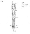
- FIG. 4 is test A for resistance increase rate measurement.
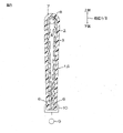
- FIG. 5 is Test B for resistance increase rate measurement.
- Electrode 1 As shown in FIG. 1, electrode 1 has a predetermined thickness.
- the electrode 1 has a film shape (including a sheet shape) extending in the surface direction.
- the plane direction is perpendicular to the thickness direction.
- Electrode 1 has one surface and the other surface spaced apart from each other in the thickness direction.
- Thermal contraction rate of electrode 1 When this electrode 1 is heated at 150° C. for 1 hour, the thermal contraction rate is ⁇ 0.2% or more and 0.2% or less.
- the thermal contraction rate of the electrode 1 is less than -0.2% or more than 0.2%, the electrode 1 easily expands and contracts when the electrode 1 is bent. As a result, damage to the conductive carbon layer 4, which will be described later, cannot be suppressed, and the rate of increase in resistance of the conductive carbon layer 4 increases.
- electrode 1 is heated at 150°C in air at atmospheric pressure for 1 hour. Then, the thermal contraction rate of the electrode 1 is determined by measuring the length before and after heating.
- the thermal contraction rate of the electrode 1 is preferably ⁇ 0.15% or more, more preferably ⁇ 0.1% or more, and preferably 0.15% or less, more preferably 0.1%. It is below.
- the electrode 1 described above comprises a resin film 2, a metal base layer 3, and a conductive carbon layer 4 in order toward one side in the thickness direction.
- the electrode 1 comprises a resin film 2, a metal base layer 3 arranged on one side in the thickness direction of the resin film 2, and a conductive carbon layer 3 arranged on one side in the thickness direction of the metal base layer 3.
- layer 4 Preferably, electrode 1 comprises resin film 2 , metal underlayer 3 and conductive carbon layer 4 .
- Each layer will be described in detail below.
- the resin film 2 forms the other surface of the electrode 1 in the thickness direction.
- the resin film 2 has a film shape extending in the surface direction.
- the resin film 2 is a base film for the electrode 1 .
- the resin film 2 has flexibility, for example.
- polyester resins eg, polyethylene terephthalate, polybutylene terephthalate, and polyethylene naphthalate
- acetate resins e.g., polyethersulfone resins, polycarbonate resins, polyamide resins, and polyolefin resins (eg, polyethylene, polypropylene and polycycloolefin polymers), (meth)acrylic resins, polyvinyl chloride resins, polyvinylidene chloride resins, polystyrene resins, polyvinyl alcohol resins, polyarylate resins, and polyphenylene sulfide resins.
- polyester resin more preferably polyethylene terephthalate, is preferably used from the viewpoint of thermal stability.
- the thickness of the resin film 2 is not limited.
- the thickness of the resin film 2 is, for example, 2 ⁇ m or more, preferably 20 ⁇ m or more, and is, for example, 1000 ⁇ m or less, preferably 500 ⁇ m or less.
- Metal underlayer 3 The metal base layer 3 is in contact with one surface of the resin film 2 in the thickness direction.
- the metal underlayer 3 extends in the planar direction.
- the metal underlayer 3 is an intermediate layer positioned between the resin film 2 and the conductive carbon layer 4 .
- the material of the metal underlayer 3 is not limited.
- Examples of the material of the metal underlayer 3 include metal elements classified into groups 3 to 14 in the periodic table defined by IUPAC in 2019, and titanium is preferable from the viewpoint of chemical stability. mentioned.
- the thickness of the metal underlayer 3 is not limited.
- the thickness of the metal underlayer 3 is, for example, 1 nm or more, preferably 5 nm or more, and 100 nm or less, preferably 50 nm or less.
- the conductive carbon layer 4 has conductivity.
- the conductive carbon layer 4 forms one surface of the electrode 1 in the thickness direction.
- the conductive carbon layer 4 is in contact with one surface of the metal underlayer 3 in the thickness direction.
- the conductive carbon layer 4 extends in the planar direction.
- the conductive carbon layer 4 has, for example, at least sp 3 bonds. Specifically, the conductive carbon layer 4 contains carbon having at least sp3 bonds. In other words, the conductive carbon layer 4 has at least a diamond structure. Thereby, the conductive carbon layer 4 has high sensitivity to the object to be measured.
- Conductive carbon layer 4 preferably has sp 2 and sp 3 bonds. Specifically, more specifically, the conductive carbon layer 4 contains carbon with sp2 bonds and carbon with sp3 bonds. In other words, the conductive carbon layer 4 has a graphite type structure and a diamond structure. As a result, the conductive carbon layer 4 has excellent conductivity and high sensitivity to the object to be measured.
- the conductive carbon layer 4 can contain, for example, oxygen in addition to carbon.
- one side of the conductive carbon layer 4 in the thickness direction contains, for example, oxygen.
- the concentration ratio of oxygen to carbon (O/C) on one surface in the thickness direction of the conductive carbon layer 4 is not limited.
- the conductive carbon layer 4 is allowed to contain a small amount of unavoidable impurities other than oxygen.
- the ratio of the number of sp 3 -bonded atoms to the sum of the number of sp 3 -bonded atoms and the number of sp 2 -bonded atoms is, for example, It is 0.10 or more, preferably 0.20 or more, preferably 0.30 or more, more preferably 0.35 or more. If the ratio of the number of sp 3 -bonded atoms (sp 3 /sp 3 +sp 2 ) is equal to or higher than the above lower limit, the potential window of the electrode 1 can be widened.
- the ratio of the number of sp 3 -bonded atoms to the sum of the number of sp 3 -bonded atoms and the number of sp 2 -bonded atoms is, for example, 0.9 or less, Preferably, it is 0.6 or less. If the ratio of the number of sp 3 -bonded atoms (sp 3 /sp 3 +sp 2 ) is equal to or less than the above upper limit, the conductivity of the conductive carbon layer 4 is ensured, and the decrease in the detection sensitivity of the electrode 1 is suppressed. can.
- the ratio of the number of sp 3 -bonded atoms is the sp 2 bond in the spectrum obtained by measuring one surface of the conductive carbon layer 4 in the thickness direction by X-ray photoelectron spectroscopy. and the peak intensity of sp3 binding.
- the density of the conductive carbon layer 4 is, for example, 1.8 g/cm 3 or more, preferably 2.0 g/cm 3 or more, more preferably 2.1 g/cm 3 or more, still more preferably 2.2 g/cm 3 or more. cm 3 or more. If the density of the conductive carbon layer 4 is equal to or higher than the above lower limit, the potential window can be widened based on the high ratio of the number of sp 3 -bonded atoms (sp 3 /sp 3 +sp 2 ). Also, the density of the conductive carbon layer 4 is, for example, 4.0 g/cm 3 or less. The density of the conductive carbon layer 4 is obtained by the X-ray reflectance method.
- the surface resistance of one side of the conductive carbon layer 4 in the thickness direction is, for example, 1.0 ⁇ 10 4 ⁇ / ⁇ or less, preferably 1.0 ⁇ 10 3 ⁇ / ⁇ or less.
- the lower limit of the surface resistance of the conductive carbon layer 4 is not limited.
- the thickness of the conductive carbon layer 4 is, for example, 0.1 nm or more, preferably 0.2 nm or more, and 100 nm or less, preferably 50 nm or less.
- the thickness of the electrode 1 is the total thickness of the resin film 2, the metal base layer 3 and the conductive carbon layer 4. Specifically, it is, for example, 2 ⁇ m or more, preferably 20 ⁇ m or more, or, for example, 1000 ⁇ m. Below, it is preferably 500 ⁇ m or less.
- the method for manufacturing the electrode 1 includes first to fourth steps. In this manufacturing method, the first to fourth steps are performed in order.
- the heating of the resin film 2 is a process for making the thermal shrinkage rate of the electrode 1 -0.2% or more and 0.2% or less. Heating conditions are not limited.
- the temperature is, for example, 70° C. or higher, preferably 100° C. or higher, more preferably 130° C. or higher, and is, for example, 200° C. or lower, preferably 180° C. or lower, more preferably 160° C. or lower.
- the time is, for example, 5 minutes or longer, preferably 15 minutes or longer, more preferably 30 minutes or longer, and for example, 10 hours or longer, preferably 5 hours or longer, more preferably 2 hours or longer.
- Heating is carried out under normal pressure (0.1 Ma) or reduced pressure (less than 0.1 MPa).
- the atmosphere is air or an inert gas (including argon).
- the metal base layer 3 is formed on one surface of the resin film 2 in the thickness direction.
- a method for forming the metal underlying layer 3 is not limited. Examples of a method for forming the metal underlayer 3 include a dry method, preferably a PVD method, and more preferably a sputtering method.
- the conductive carbon layer 4 is formed on one surface of the metal underlayer 3 in the thickness direction.
- a method for forming the conductive carbon layer 4 include a dry method. Dry methods include, for example, PVD (physical vapor deposition) and CVD (chemical vapor deposition), preferably PVD. Examples of PVD methods include sputtering, vacuum deposition, laser deposition, and ion plating (including arc deposition). Sputtering is preferred.
- Examples of sputtering methods include unbalanced magnetron sputtering (UBM sputtering), high-power pulse sputtering, electron cyclotron resonance sputtering, RF sputtering, DC sputtering, DC pulse sputtering, and ion beam sputtering. is mentioned. From the viewpoint that the ratio of the number of sp 3 -bonded atoms can be easily set within the desired range described above, DC sputtering is more preferred, and DC magnetron sputtering is even more preferred.
- UBM sputtering unbalanced magnetron sputtering
- high-power pulse sputtering electron cyclotron resonance sputtering
- RF sputtering electron cyclotron resonance sputtering
- DC sputtering DC sputtering
- DC pulse sputtering DC pulse sputtering
- ion beam sputtering ion beam
- Sintered carbon for example, can be used as a target in the sputtering method.
- the sputtering gas include inert gases.
- the inert gas contains Ar.
- the pressure in sputtering is, for example, 1 Pa or less.
- the film formation temperature is, for example, 0° C. or lower, for example, 150° C. or lower.
- the electrode 1 described above is obtained by performing the first to fourth steps.
- the electrode 1 can be used as various electrodes, and is preferably an electrode for electrochemical measurements that perform an electrochemical measurement method, specifically a working electrode (working electrode) that performs cyclic voltammetry (CV) or , can be used as a working electrode for performing anodic-stripping-voltammetry (ASV).
- a working electrode working electrode
- CV cyclic voltammetry
- ASV anodic-stripping-voltammetry
- the electrode 1 can be used in a curved manner in view of the effects described later. Specifically, the electrode 1 can be used by being fixed on a curved wall surface or pasted on a rod-shaped substrate.
- This electrode 1 has a thermal contraction rate of -0.2% or more and 0.2% or less, which is 0. Therefore, even if it is bent, damage to the conductive carbon layer 4 can be suppressed, and resistance increases before and after bending. rate can be controlled.
- the ratio of the number of sp 3 -bonded atoms to the sum of the number of sp 3 -bonded atoms and the number of sp 2 -bonded atoms is 0.10 or more, the potential window of the electrode 1 can be widened.
- the conductive carbon layer 4 has a density of 1.8 g/cm 3 or more, the ratio of the number of sp 3 bonded atoms (sp 3 /sp 3 +sp 2 ) is high. , the potential window can be widened.
- the heat shrinkage rate of the electrode 1 is adjusted to be -0.2% or more and 0.2% or less.
- 2 can also be prepared.
- a resin having a molecular structure with a low thermal shrinkage rate is used as a raw material, or the thermal shrinkage rate of the resin film 2 itself is reduced by heating or suppressing the tension during transportation at the stage of molding the resin film 2 from the raw material. You can also suppress it.
- the electrode 1 includes one resin film 2, one metal underlayer 3, and one conductive carbon layer 4.
- one resin film 2, two metal underlayers 3, and two conductive carbon layers 4 may be provided. That is, the electrode 1 can have two metal underlayers 3 and two conductive carbon layers 4 for one resin film 2 .
- the conductive carbon layer 4, the metal base layer 3, the resin film 2, the metal base layer 3, and the conductive carbon layer 4 are arranged in order toward one side in the thickness direction.
- the electrode 1 may be provided with the resin film 2 and the conductive carbon layer 4 in this order on one side in the thickness direction without the metal base layer 3 .
- Examples and comparative examples are shown below to describe the present invention more specifically.
- the present invention is not limited to Examples and Comparative Examples. Specific numerical values such as the mixing ratio (content ratio), physical property values, parameters, etc. used in the following description are described in the above "Mode for Carrying Out the Invention", the corresponding mixing ratio (content ratio ), physical properties, parameters, etc. can. In the description below, “parts” and “%” are based on mass unless otherwise specified.
- Example 1 A resin film 2 made of polyethylene terephthalate and having a thickness of 50 ⁇ m was prepared (first step).
- the resin film 2 was heated in a heating oven at 120°C for 1 hour (second step).
- a metal base layer 3 made of titanium was formed on one surface of the resin film 2 in the thickness direction by DC magnetron sputtering (third step).
- the conditions for DC magnetron sputtering are as follows.
- Target material Titanium Target power: 100W Sputtering gas: Argon Sputtering chamber pressure: 0.2 Pa
- the thickness of the metal underlayer 3 was 12 nm.
- a conductive carbon layer 4 was formed on one side of the metal underlayer in the thickness direction by DC pulse magnetron sputtering (fourth step).
- the conditions for DC pulse magnetron sputtering are as follows.
- Target material sintered carbon Argon gas pressure: 0.4 Pa
- Target power 2.0 W/cm 2
- Temperature 120°C or less
- the surface resistance of the conductive carbon layer 4 was 1.0 ⁇ 10 2 ⁇ / ⁇ .
- the sp 3 ratio (sp 3 /sp 3 +sp 2 ) in the conductive carbon layer 4 was 0.35, and the density was 2.1 g/cm 3 .
- the thickness of the conductive carbon layer 4 was 40 nm.
- the electrode 1 was manufactured. Since the electrode 1 is manufactured by the roll-to-roll method described above, it has MD and TD directions.
- Electrode 1 was manufactured in the same manner as in Example 1. However, the heating temperature in the second step was changed from 120°C to 150°C.
- Electrode 1 was manufactured in the same manner as in Example 2. However, the conditions of the fourth step were changed as follows. Argon gas pressure: 0.2 Pa Target power: 1.7 W/cm 2
- the surface resistance of the conductive carbon layer 4 was 140 ⁇ / ⁇ .
- the sp 3 ratio (sp 3 /sp 3 +sp 2 ) in the conductive carbon layer 4 was 0.45, and the density was 2.3 g/cm 3 .
- the thickness of the conductive carbon layer 4 was 40 nm.
- Electrode 1 was manufactured in the same manner as in Example 2. However, the conditions of the fourth step were changed as follows. Argon gas pressure: 2 Pa Target power: 1.1W/cm2
- the surface resistance of the conductive carbon layer 4 was 160 ⁇ / ⁇ .
- the sp 3 ratio (sp 3 /sp 3 +sp 2 ) in the conductive carbon layer 4 was 0.30, and the density was 1.8 g/cm 3 .
- the thickness of the conductive carbon layer 4 was 40 nm.
- Electrode 1 was manufactured in the same manner as in Example 1. However, the second step was not performed.
- Electrode 1 was manufactured in the same manner as in Example 3. However, the second step was not performed.
- Electrode 1 was manufactured in the same manner as in Example 4. However, the second step was not performed.
- Table 1 shows the conditions or presence/absence of the second step, the density of the conductive carbon layer 4, and the ratio of the number of sp 3 -bonded atoms (sp 3 /sp 3 +sp 2 ) for each example and each comparative example. Describe.
- Electrode 1 was subjected to the following evaluations. Those results are shown in Table 1.
- Heat shrinkage rate of resin film 2 A sample was prepared by cutting the electrode 1 into a square having a side length of 30 mm. The samples were then heated in a heating oven at 150° C. for 1 hour. The dimensions of the electrode 1 before and after heating were measured with an image dimension measuring instrument (IM-6020, manufactured by Keyence), and the thermal shrinkage rate was obtained from the following formula.
- Thermal shrinkage rate [%] (length in MD direction after heating - length in MD direction before heating) / length in MD direction before heating x 100
- the heat shrinkage rate in the MD direction is higher than the heat shrinkage rate in the TD direction, so the heat shrinkage rate in the MD direction is evaluated above.
- evaluation should be performed in the direction in which the absolute value of the thermal shrinkage is large.
- the methods described above include batch mode.
- a sample 5 was prepared by cutting the electrode 1 into a strip having a length of 70 mm in the longitudinal direction and a length of 20 mm in the lateral direction.
- the longitudinal direction is along the MD direction.
- the sample 5 was bent so that both ends 6 of the sample 5 in the longitudinal direction approached each other.
- the longitudinal central portion 7 of the sample 5 was wound around a metal rod 8 having a diameter of 6.5 mm. Both ends 6 of the sample 5 in the longitudinal direction were fixed with a clip 10 to which a weight 9 of 150 g was attached, and held for 10 seconds.
- the surface resistance of the electrode 1 at the center portion 7 before and after the bending was measured, and the resistance increase rate was obtained by the following formula.
- Resistance increase rate [%] (Surface resistance of electrode 1 in central portion 7 after bending - Surface resistance of electrode 1 in central portion 7 before bending)/Surface resistance of electrode 1 in central portion 7 before bending ⁇ 100
- Test A A test in which the resin films 2 face each other when the sample 5 is wound around the clip 10 as shown in FIG.
- the rod 8, the resin film 2, the metal base layer 3, and the conductive carbon layer 4 are arranged in order toward the upper side.
- a tensile force acts on the conductive carbon layer 4 in the central portion.
- test B a test in which the conductive carbon layers 4 face each other as shown in FIG.
- the rod 8, the conductive carbon layer 4, the metal base layer 3, and the resin film 2 are arranged in order toward the upper side.
- a compressive force acts on the conductive carbon layer 4 in the central portion.
- the electrodes are used as electrodes for electrochemical measurements.
Landscapes
- Chemical & Material Sciences (AREA)
- Chemical Kinetics & Catalysis (AREA)
- Organic Chemistry (AREA)
- Health & Medical Sciences (AREA)
- Life Sciences & Earth Sciences (AREA)
- Engineering & Computer Science (AREA)
- Materials Engineering (AREA)
- Electrochemistry (AREA)
- Mechanical Engineering (AREA)
- Metallurgy (AREA)
- Analytical Chemistry (AREA)
- Pathology (AREA)
- Molecular Biology (AREA)
- Biochemistry (AREA)
- General Health & Medical Sciences (AREA)
- General Physics & Mathematics (AREA)
- Immunology (AREA)
- Physics & Mathematics (AREA)
- Inorganic Chemistry (AREA)
- General Chemical & Material Sciences (AREA)
- Laminated Bodies (AREA)
- Electric Double-Layer Capacitors Or The Like (AREA)
- Non-Insulated Conductors (AREA)
- Inert Electrodes (AREA)
Priority Applications (4)
| Application Number | Priority Date | Filing Date | Title |
|---|---|---|---|
| US18/283,087 US20240167976A1 (en) | 2021-03-23 | 2022-03-18 | Electrode |
| JP2023509150A JP7798863B2 (ja) | 2021-03-23 | 2022-03-18 | 電極 |
| EP22775502.2A EP4317958A4 (en) | 2021-03-23 | 2022-03-18 | ELECTRODE |
| JP2025281834A JP2026042820A (ja) | 2021-03-23 | 2025-12-25 | 電極 |
Applications Claiming Priority (4)
| Application Number | Priority Date | Filing Date | Title |
|---|---|---|---|
| JP2021-048722 | 2021-03-23 | ||
| JP2021048722 | 2021-03-23 | ||
| JP2022033622 | 2022-03-04 | ||
| JP2022-033622 | 2022-03-04 |
Publications (1)
| Publication Number | Publication Date |
|---|---|
| WO2022202715A1 true WO2022202715A1 (ja) | 2022-09-29 |
Family
ID=83397316
Family Applications (1)
| Application Number | Title | Priority Date | Filing Date |
|---|---|---|---|
| PCT/JP2022/012852 Ceased WO2022202715A1 (ja) | 2021-03-23 | 2022-03-18 | 電極 |
Country Status (4)
| Country | Link |
|---|---|
| US (1) | US20240167976A1 (https=) |
| EP (1) | EP4317958A4 (https=) |
| JP (2) | JP7798863B2 (https=) |
| WO (1) | WO2022202715A1 (https=) |
Cited By (1)
| Publication number | Priority date | Publication date | Assignee | Title |
|---|---|---|---|---|
| WO2024203071A1 (ja) * | 2023-03-27 | 2024-10-03 | 日東電工株式会社 | 電極 |
Citations (6)
| Publication number | Priority date | Publication date | Assignee | Title |
|---|---|---|---|---|
| WO2016013478A1 (ja) | 2014-07-22 | 2016-01-28 | 東洋紡株式会社 | 薄膜積層フィルム |
| JP2019105637A (ja) * | 2017-12-11 | 2019-06-27 | 日東電工株式会社 | 電極フィルムおよび電気化学測定システム |
| JP2020144116A (ja) * | 2019-02-28 | 2020-09-10 | 日東電工株式会社 | 電極および電気化学測定システム |
| WO2020196587A1 (ja) * | 2019-03-28 | 2020-10-01 | 日東電工株式会社 | 電極および電気化学測定システム |
| WO2021193631A1 (ja) * | 2020-03-26 | 2021-09-30 | 日東電工株式会社 | 電極 |
| JP6970861B1 (ja) * | 2020-03-19 | 2021-11-24 | 日東電工株式会社 | 透明導電性フィルム、および透明導電性フィルムの製造方法 |
Family Cites Families (1)
| Publication number | Priority date | Publication date | Assignee | Title |
|---|---|---|---|---|
| EP4650766A3 (en) * | 2017-12-11 | 2026-01-14 | Nitto Denko Corporation | Electrode film and electrochemical measurement system |
-
2022
- 2022-03-18 WO PCT/JP2022/012852 patent/WO2022202715A1/ja not_active Ceased
- 2022-03-18 JP JP2023509150A patent/JP7798863B2/ja active Active
- 2022-03-18 US US18/283,087 patent/US20240167976A1/en active Pending
- 2022-03-18 EP EP22775502.2A patent/EP4317958A4/en active Pending
-
2025
- 2025-12-25 JP JP2025281834A patent/JP2026042820A/ja active Pending
Patent Citations (6)
| Publication number | Priority date | Publication date | Assignee | Title |
|---|---|---|---|---|
| WO2016013478A1 (ja) | 2014-07-22 | 2016-01-28 | 東洋紡株式会社 | 薄膜積層フィルム |
| JP2019105637A (ja) * | 2017-12-11 | 2019-06-27 | 日東電工株式会社 | 電極フィルムおよび電気化学測定システム |
| JP2020144116A (ja) * | 2019-02-28 | 2020-09-10 | 日東電工株式会社 | 電極および電気化学測定システム |
| WO2020196587A1 (ja) * | 2019-03-28 | 2020-10-01 | 日東電工株式会社 | 電極および電気化学測定システム |
| JP6970861B1 (ja) * | 2020-03-19 | 2021-11-24 | 日東電工株式会社 | 透明導電性フィルム、および透明導電性フィルムの製造方法 |
| WO2021193631A1 (ja) * | 2020-03-26 | 2021-09-30 | 日東電工株式会社 | 電極 |
Non-Patent Citations (1)
| Title |
|---|
| See also references of EP4317958A4 |
Cited By (1)
| Publication number | Priority date | Publication date | Assignee | Title |
|---|---|---|---|---|
| WO2024203071A1 (ja) * | 2023-03-27 | 2024-10-03 | 日東電工株式会社 | 電極 |
Also Published As
| Publication number | Publication date |
|---|---|
| TW202302335A (zh) | 2023-01-16 |
| JP7798863B2 (ja) | 2026-01-14 |
| US20240167976A1 (en) | 2024-05-23 |
| EP4317958A1 (en) | 2024-02-07 |
| JP2026042820A (ja) | 2026-03-11 |
| JPWO2022202715A1 (https=) | 2022-09-29 |
| EP4317958A4 (en) | 2025-03-26 |
Similar Documents
| Publication | Publication Date | Title |
|---|---|---|
| JP2026042820A (ja) | 電極 | |
| US7460352B2 (en) | Flexible dielectric film and method for making | |
| Hu et al. | The effect of duty cycle and bias voltage for graphite-like carbon film coated 304 stainless steel as metallic bipolar plate | |
| CN1836338A (zh) | 新型金属带产品 | |
| JP5833587B2 (ja) | ステンレス鋼を母材とする耐食性及び伝導性ナノカーボンコーティング方法及びそれによる燃料電池分離板の製造方法 | |
| Yang et al. | Field emission from zinc oxide nanoneedles on plastic substrates | |
| KR102328694B1 (ko) | 다층 그래핀 적층체, 이의 제조방법 및 이를 이용한 전자 소자 | |
| US20150064571A1 (en) | Current collector structure | |
| KR101877500B1 (ko) | 대면적 그래핀 박막의 in-situ 제조방법 | |
| Li et al. | The improvement of the field emission properties from graphene films: Ti transition layer and annealing process | |
| CN115398217A (zh) | 电极 | |
| CN107740058A (zh) | 具有垂直阵列结构的金属/非金属复合薄膜的制备方法 | |
| CN104089570B (zh) | 一种压阻传感元件及其制备方法 | |
| US12590855B2 (en) | Strain sensor, functional film, and method for manufacturing same | |
| JP5295102B2 (ja) | 導電性保護膜及びその製造方法 | |
| JP2009164412A (ja) | 多孔質金属薄膜およびその製造方法、ならびにコンデンサ | |
| WO2022202941A1 (ja) | 電極およびその製造方法 | |
| TWI918900B (zh) | 電極 | |
| CN108292667A (zh) | 经涂覆的柔性组件 | |
| CN116457655A (zh) | 电极 | |
| JP2002343150A (ja) | 透明導電性フィルム及びその製造方法 | |
| KR101695590B1 (ko) | 티타늄금속기판 위에 다이아몬드 코팅층이 형성된 수처리용 구조재 및 그 제조 방법 | |
| CN103643085A (zh) | 埋入式薄膜电阻材料及其制备方法 | |
| CN116438062A (zh) | 层叠薄膜、第2层叠薄膜的制造方法和应变传感器的制造方法 | |
| WO2022092207A1 (ja) | 積層フィルムおよび歪みセンサの製造方法 |
Legal Events
| Date | Code | Title | Description |
|---|---|---|---|
| 121 | Ep: the epo has been informed by wipo that ep was designated in this application |
Ref document number: 22775502 Country of ref document: EP Kind code of ref document: A1 |
|
| WWE | Wipo information: entry into national phase |
Ref document number: 2023509150 Country of ref document: JP |
|
| WWE | Wipo information: entry into national phase |
Ref document number: 18283087 Country of ref document: US |
|
| WWE | Wipo information: entry into national phase |
Ref document number: 2022775502 Country of ref document: EP |
|
| NENP | Non-entry into the national phase |
Ref country code: DE |
|
| ENP | Entry into the national phase |
Ref document number: 2022775502 Country of ref document: EP Effective date: 20231023 |