WO2022190942A1 - 銅被覆アルミニウム線材およびその製造方法 - Google Patents
銅被覆アルミニウム線材およびその製造方法 Download PDFInfo
- Publication number
- WO2022190942A1 WO2022190942A1 PCT/JP2022/008429 JP2022008429W WO2022190942A1 WO 2022190942 A1 WO2022190942 A1 WO 2022190942A1 JP 2022008429 W JP2022008429 W JP 2022008429W WO 2022190942 A1 WO2022190942 A1 WO 2022190942A1
- Authority
- WO
- WIPO (PCT)
- Prior art keywords
- copper
- aluminum wire
- aluminum
- thin film
- less
- Prior art date
Links
- 229910052782 aluminium Inorganic materials 0.000 title claims abstract description 218
- XAGFODPZIPBFFR-UHFFFAOYSA-N aluminium Chemical compound [Al] XAGFODPZIPBFFR-UHFFFAOYSA-N 0.000 title claims abstract description 218
- 239000010949 copper Substances 0.000 title claims abstract description 197
- 229910052802 copper Inorganic materials 0.000 title claims abstract description 192
- RYGMFSIKBFXOCR-UHFFFAOYSA-N Copper Chemical compound [Cu] RYGMFSIKBFXOCR-UHFFFAOYSA-N 0.000 title claims abstract description 191
- 238000004519 manufacturing process Methods 0.000 title claims abstract description 16
- 239000000463 material Substances 0.000 title abstract description 7
- 229910000838 Al alloy Inorganic materials 0.000 claims abstract description 18
- 238000012360 testing method Methods 0.000 claims abstract description 9
- 239000010409 thin film Substances 0.000 claims description 66
- 238000000034 method Methods 0.000 claims description 42
- 238000001704 evaporation Methods 0.000 claims description 31
- 239000010408 film Substances 0.000 claims description 29
- 230000008020 evaporation Effects 0.000 claims description 27
- 238000007733 ion plating Methods 0.000 claims description 21
- XKRFYHLGVUSROY-UHFFFAOYSA-N argon Substances [Ar] XKRFYHLGVUSROY-UHFFFAOYSA-N 0.000 claims description 15
- 238000010849 ion bombardment Methods 0.000 claims description 12
- 238000005491 wire drawing Methods 0.000 claims description 12
- JPVYNHNXODAKFH-UHFFFAOYSA-N Cu2+ Chemical compound [Cu+2] JPVYNHNXODAKFH-UHFFFAOYSA-N 0.000 claims description 11
- 229910001431 copper ion Inorganic materials 0.000 claims description 11
- 239000011651 chromium Substances 0.000 claims description 10
- 239000011777 magnesium Substances 0.000 claims description 10
- 239000011572 manganese Substances 0.000 claims description 10
- 239000010936 titanium Substances 0.000 claims description 10
- 229910052786 argon Inorganic materials 0.000 claims description 9
- 238000010894 electron beam technology Methods 0.000 claims description 9
- 238000004804 winding Methods 0.000 claims description 9
- 238000010438 heat treatment Methods 0.000 claims description 7
- ZOXJGFHDIHLPTG-UHFFFAOYSA-N Boron Chemical compound [B] ZOXJGFHDIHLPTG-UHFFFAOYSA-N 0.000 claims description 5
- VYZAMTAEIAYCRO-UHFFFAOYSA-N Chromium Chemical compound [Cr] VYZAMTAEIAYCRO-UHFFFAOYSA-N 0.000 claims description 5
- XEEYBQQBJWHFJM-UHFFFAOYSA-N Iron Chemical compound [Fe] XEEYBQQBJWHFJM-UHFFFAOYSA-N 0.000 claims description 5
- WHXSMMKQMYFTQS-UHFFFAOYSA-N Lithium Chemical compound [Li] WHXSMMKQMYFTQS-UHFFFAOYSA-N 0.000 claims description 5
- FYYHWMGAXLPEAU-UHFFFAOYSA-N Magnesium Chemical compound [Mg] FYYHWMGAXLPEAU-UHFFFAOYSA-N 0.000 claims description 5
- PWHULOQIROXLJO-UHFFFAOYSA-N Manganese Chemical compound [Mn] PWHULOQIROXLJO-UHFFFAOYSA-N 0.000 claims description 5
- XUIMIQQOPSSXEZ-UHFFFAOYSA-N Silicon Chemical compound [Si] XUIMIQQOPSSXEZ-UHFFFAOYSA-N 0.000 claims description 5
- RTAQQCXQSZGOHL-UHFFFAOYSA-N Titanium Chemical compound [Ti] RTAQQCXQSZGOHL-UHFFFAOYSA-N 0.000 claims description 5
- 229910052796 boron Inorganic materials 0.000 claims description 5
- 229910052804 chromium Inorganic materials 0.000 claims description 5
- 229910052744 lithium Inorganic materials 0.000 claims description 5
- 229910052749 magnesium Inorganic materials 0.000 claims description 5
- 229910052748 manganese Inorganic materials 0.000 claims description 5
- 229910052706 scandium Inorganic materials 0.000 claims description 5
- SIXSYDAISGFNSX-UHFFFAOYSA-N scandium atom Chemical compound [Sc] SIXSYDAISGFNSX-UHFFFAOYSA-N 0.000 claims description 5
- VSZWPYCFIRKVQL-UHFFFAOYSA-N selanylidenegallium;selenium Chemical compound [Se].[Se]=[Ga].[Se]=[Ga] VSZWPYCFIRKVQL-UHFFFAOYSA-N 0.000 claims description 5
- 229910052710 silicon Inorganic materials 0.000 claims description 5
- 239000010703 silicon Substances 0.000 claims description 5
- JBQYATWDVHIOAR-UHFFFAOYSA-N tellanylidenegermanium Chemical compound [Te]=[Ge] JBQYATWDVHIOAR-UHFFFAOYSA-N 0.000 claims description 5
- 229910052719 titanium Inorganic materials 0.000 claims description 5
- 238000004140 cleaning Methods 0.000 claims description 4
- 229910003460 diamond Inorganic materials 0.000 claims description 4
- 239000010432 diamond Substances 0.000 claims description 4
- -1 argon ions Chemical class 0.000 claims description 3
- 239000011248 coating agent Substances 0.000 claims description 3
- 238000000576 coating method Methods 0.000 claims description 3
- 229910045601 alloy Inorganic materials 0.000 claims description 2
- 239000000956 alloy Substances 0.000 claims description 2
- 150000001879 copper Chemical class 0.000 abstract 1
- 238000010586 diagram Methods 0.000 description 15
- 239000002245 particle Substances 0.000 description 8
- 238000001878 scanning electron micrograph Methods 0.000 description 7
- 230000015572 biosynthetic process Effects 0.000 description 6
- 239000007789 gas Substances 0.000 description 6
- 238000007740 vapor deposition Methods 0.000 description 5
- 238000002161 passivation Methods 0.000 description 4
- 229910052751 metal Inorganic materials 0.000 description 3
- 239000002184 metal Substances 0.000 description 3
- XLYOFNOQVPJJNP-UHFFFAOYSA-N water Substances O XLYOFNOQVPJJNP-UHFFFAOYSA-N 0.000 description 3
- 238000000137 annealing Methods 0.000 description 2
- 238000000151 deposition Methods 0.000 description 2
- 230000008021 deposition Effects 0.000 description 2
- 230000003287 optical effect Effects 0.000 description 2
- 238000012545 processing Methods 0.000 description 2
- 241001424392 Lucia limbaria Species 0.000 description 1
- ZOKXTWBITQBERF-UHFFFAOYSA-N Molybdenum Chemical compound [Mo] ZOKXTWBITQBERF-UHFFFAOYSA-N 0.000 description 1
- HCHKCACWOHOZIP-UHFFFAOYSA-N Zinc Chemical compound [Zn] HCHKCACWOHOZIP-UHFFFAOYSA-N 0.000 description 1
- 230000004913 activation Effects 0.000 description 1
- QVGXLLKOCUKJST-UHFFFAOYSA-N atomic oxygen Chemical compound [O] QVGXLLKOCUKJST-UHFFFAOYSA-N 0.000 description 1
- 238000004891 communication Methods 0.000 description 1
- 239000004020 conductor Substances 0.000 description 1
- 238000005260 corrosion Methods 0.000 description 1
- 230000007797 corrosion Effects 0.000 description 1
- 238000009792 diffusion process Methods 0.000 description 1
- 238000006073 displacement reaction Methods 0.000 description 1
- 238000009713 electroplating Methods 0.000 description 1
- 230000007613 environmental effect Effects 0.000 description 1
- HJUFTIJOISQSKQ-UHFFFAOYSA-N fenoxycarb Chemical compound C1=CC(OCCNC(=O)OCC)=CC=C1OC1=CC=CC=C1 HJUFTIJOISQSKQ-UHFFFAOYSA-N 0.000 description 1
- 239000000446 fuel Substances 0.000 description 1
- 230000005484 gravity Effects 0.000 description 1
- 230000012447 hatching Effects 0.000 description 1
- 150000002500 ions Chemical class 0.000 description 1
- 239000002932 luster Substances 0.000 description 1
- 150000002739 metals Chemical class 0.000 description 1
- 238000012986 modification Methods 0.000 description 1
- 230000004048 modification Effects 0.000 description 1
- 229910052750 molybdenum Inorganic materials 0.000 description 1
- 239000011733 molybdenum Substances 0.000 description 1
- 238000000879 optical micrograph Methods 0.000 description 1
- 239000001301 oxygen Substances 0.000 description 1
- 229910052760 oxygen Inorganic materials 0.000 description 1
- 238000007747 plating Methods 0.000 description 1
- 230000001737 promoting effect Effects 0.000 description 1
- 229910000679 solder Inorganic materials 0.000 description 1
- 229910052715 tantalum Inorganic materials 0.000 description 1
- GUVRBAGPIYLISA-UHFFFAOYSA-N tantalum atom Chemical compound [Ta] GUVRBAGPIYLISA-UHFFFAOYSA-N 0.000 description 1
- WFKWXMTUELFFGS-UHFFFAOYSA-N tungsten Chemical compound [W] WFKWXMTUELFFGS-UHFFFAOYSA-N 0.000 description 1
- 229910052721 tungsten Inorganic materials 0.000 description 1
- 239000010937 tungsten Substances 0.000 description 1
- 239000011701 zinc Substances 0.000 description 1
- 229910052725 zinc Inorganic materials 0.000 description 1
- NWONKYPBYAMBJT-UHFFFAOYSA-L zinc sulfate Chemical compound [Zn+2].[O-]S([O-])(=O)=O NWONKYPBYAMBJT-UHFFFAOYSA-L 0.000 description 1
Images


Classifications
-
- C—CHEMISTRY; METALLURGY
- C23—COATING METALLIC MATERIAL; COATING MATERIAL WITH METALLIC MATERIAL; CHEMICAL SURFACE TREATMENT; DIFFUSION TREATMENT OF METALLIC MATERIAL; COATING BY VACUUM EVAPORATION, BY SPUTTERING, BY ION IMPLANTATION OR BY CHEMICAL VAPOUR DEPOSITION, IN GENERAL; INHIBITING CORROSION OF METALLIC MATERIAL OR INCRUSTATION IN GENERAL
- C23C—COATING METALLIC MATERIAL; COATING MATERIAL WITH METALLIC MATERIAL; SURFACE TREATMENT OF METALLIC MATERIAL BY DIFFUSION INTO THE SURFACE, BY CHEMICAL CONVERSION OR SUBSTITUTION; COATING BY VACUUM EVAPORATION, BY SPUTTERING, BY ION IMPLANTATION OR BY CHEMICAL VAPOUR DEPOSITION, IN GENERAL
- C23C28/00—Coating for obtaining at least two superposed coatings either by methods not provided for in a single one of groups C23C2/00 - C23C26/00 or by combinations of methods provided for in subclasses C23C and C25C or C25D
- C23C28/30—Coatings combining at least one metallic layer and at least one inorganic non-metallic layer
- C23C28/32—Coatings combining at least one metallic layer and at least one inorganic non-metallic layer including at least one pure metallic layer
- C23C28/322—Coatings combining at least one metallic layer and at least one inorganic non-metallic layer including at least one pure metallic layer only coatings of metal elements only
-
- C—CHEMISTRY; METALLURGY
- C23—COATING METALLIC MATERIAL; COATING MATERIAL WITH METALLIC MATERIAL; CHEMICAL SURFACE TREATMENT; DIFFUSION TREATMENT OF METALLIC MATERIAL; COATING BY VACUUM EVAPORATION, BY SPUTTERING, BY ION IMPLANTATION OR BY CHEMICAL VAPOUR DEPOSITION, IN GENERAL; INHIBITING CORROSION OF METALLIC MATERIAL OR INCRUSTATION IN GENERAL
- C23C—COATING METALLIC MATERIAL; COATING MATERIAL WITH METALLIC MATERIAL; SURFACE TREATMENT OF METALLIC MATERIAL BY DIFFUSION INTO THE SURFACE, BY CHEMICAL CONVERSION OR SUBSTITUTION; COATING BY VACUUM EVAPORATION, BY SPUTTERING, BY ION IMPLANTATION OR BY CHEMICAL VAPOUR DEPOSITION, IN GENERAL
- C23C14/00—Coating by vacuum evaporation, by sputtering or by ion implantation of the coating forming material
- C23C14/02—Pretreatment of the material to be coated
- C23C14/021—Cleaning or etching treatments
- C23C14/022—Cleaning or etching treatments by means of bombardment with energetic particles or radiation
-
- C—CHEMISTRY; METALLURGY
- C23—COATING METALLIC MATERIAL; COATING MATERIAL WITH METALLIC MATERIAL; CHEMICAL SURFACE TREATMENT; DIFFUSION TREATMENT OF METALLIC MATERIAL; COATING BY VACUUM EVAPORATION, BY SPUTTERING, BY ION IMPLANTATION OR BY CHEMICAL VAPOUR DEPOSITION, IN GENERAL; INHIBITING CORROSION OF METALLIC MATERIAL OR INCRUSTATION IN GENERAL
- C23C—COATING METALLIC MATERIAL; COATING MATERIAL WITH METALLIC MATERIAL; SURFACE TREATMENT OF METALLIC MATERIAL BY DIFFUSION INTO THE SURFACE, BY CHEMICAL CONVERSION OR SUBSTITUTION; COATING BY VACUUM EVAPORATION, BY SPUTTERING, BY ION IMPLANTATION OR BY CHEMICAL VAPOUR DEPOSITION, IN GENERAL
- C23C14/00—Coating by vacuum evaporation, by sputtering or by ion implantation of the coating forming material
- C23C14/06—Coating by vacuum evaporation, by sputtering or by ion implantation of the coating forming material characterised by the coating material
- C23C14/14—Metallic material, boron or silicon
- C23C14/16—Metallic material, boron or silicon on metallic substrates or on substrates of boron or silicon
-
- C—CHEMISTRY; METALLURGY
- C23—COATING METALLIC MATERIAL; COATING MATERIAL WITH METALLIC MATERIAL; CHEMICAL SURFACE TREATMENT; DIFFUSION TREATMENT OF METALLIC MATERIAL; COATING BY VACUUM EVAPORATION, BY SPUTTERING, BY ION IMPLANTATION OR BY CHEMICAL VAPOUR DEPOSITION, IN GENERAL; INHIBITING CORROSION OF METALLIC MATERIAL OR INCRUSTATION IN GENERAL
- C23C—COATING METALLIC MATERIAL; COATING MATERIAL WITH METALLIC MATERIAL; SURFACE TREATMENT OF METALLIC MATERIAL BY DIFFUSION INTO THE SURFACE, BY CHEMICAL CONVERSION OR SUBSTITUTION; COATING BY VACUUM EVAPORATION, BY SPUTTERING, BY ION IMPLANTATION OR BY CHEMICAL VAPOUR DEPOSITION, IN GENERAL
- C23C14/00—Coating by vacuum evaporation, by sputtering or by ion implantation of the coating forming material
- C23C14/22—Coating by vacuum evaporation, by sputtering or by ion implantation of the coating forming material characterised by the process of coating
- C23C14/24—Vacuum evaporation
- C23C14/28—Vacuum evaporation by wave energy or particle radiation
- C23C14/30—Vacuum evaporation by wave energy or particle radiation by electron bombardment
-
- C—CHEMISTRY; METALLURGY
- C23—COATING METALLIC MATERIAL; COATING MATERIAL WITH METALLIC MATERIAL; CHEMICAL SURFACE TREATMENT; DIFFUSION TREATMENT OF METALLIC MATERIAL; COATING BY VACUUM EVAPORATION, BY SPUTTERING, BY ION IMPLANTATION OR BY CHEMICAL VAPOUR DEPOSITION, IN GENERAL; INHIBITING CORROSION OF METALLIC MATERIAL OR INCRUSTATION IN GENERAL
- C23C—COATING METALLIC MATERIAL; COATING MATERIAL WITH METALLIC MATERIAL; SURFACE TREATMENT OF METALLIC MATERIAL BY DIFFUSION INTO THE SURFACE, BY CHEMICAL CONVERSION OR SUBSTITUTION; COATING BY VACUUM EVAPORATION, BY SPUTTERING, BY ION IMPLANTATION OR BY CHEMICAL VAPOUR DEPOSITION, IN GENERAL
- C23C14/00—Coating by vacuum evaporation, by sputtering or by ion implantation of the coating forming material
- C23C14/22—Coating by vacuum evaporation, by sputtering or by ion implantation of the coating forming material characterised by the process of coating
- C23C14/24—Vacuum evaporation
- C23C14/32—Vacuum evaporation by explosion; by evaporation and subsequent ionisation of the vapours, e.g. ion-plating
-
- C—CHEMISTRY; METALLURGY
- C23—COATING METALLIC MATERIAL; COATING MATERIAL WITH METALLIC MATERIAL; CHEMICAL SURFACE TREATMENT; DIFFUSION TREATMENT OF METALLIC MATERIAL; COATING BY VACUUM EVAPORATION, BY SPUTTERING, BY ION IMPLANTATION OR BY CHEMICAL VAPOUR DEPOSITION, IN GENERAL; INHIBITING CORROSION OF METALLIC MATERIAL OR INCRUSTATION IN GENERAL
- C23C—COATING METALLIC MATERIAL; COATING MATERIAL WITH METALLIC MATERIAL; SURFACE TREATMENT OF METALLIC MATERIAL BY DIFFUSION INTO THE SURFACE, BY CHEMICAL CONVERSION OR SUBSTITUTION; COATING BY VACUUM EVAPORATION, BY SPUTTERING, BY ION IMPLANTATION OR BY CHEMICAL VAPOUR DEPOSITION, IN GENERAL
- C23C14/00—Coating by vacuum evaporation, by sputtering or by ion implantation of the coating forming material
- C23C14/58—After-treatment
- C23C14/5806—Thermal treatment
-
- C—CHEMISTRY; METALLURGY
- C23—COATING METALLIC MATERIAL; COATING MATERIAL WITH METALLIC MATERIAL; CHEMICAL SURFACE TREATMENT; DIFFUSION TREATMENT OF METALLIC MATERIAL; COATING BY VACUUM EVAPORATION, BY SPUTTERING, BY ION IMPLANTATION OR BY CHEMICAL VAPOUR DEPOSITION, IN GENERAL; INHIBITING CORROSION OF METALLIC MATERIAL OR INCRUSTATION IN GENERAL
- C23C—COATING METALLIC MATERIAL; COATING MATERIAL WITH METALLIC MATERIAL; SURFACE TREATMENT OF METALLIC MATERIAL BY DIFFUSION INTO THE SURFACE, BY CHEMICAL CONVERSION OR SUBSTITUTION; COATING BY VACUUM EVAPORATION, BY SPUTTERING, BY ION IMPLANTATION OR BY CHEMICAL VAPOUR DEPOSITION, IN GENERAL
- C23C14/00—Coating by vacuum evaporation, by sputtering or by ion implantation of the coating forming material
- C23C14/58—After-treatment
- C23C14/5886—Mechanical treatment
-
- C—CHEMISTRY; METALLURGY
- C23—COATING METALLIC MATERIAL; COATING MATERIAL WITH METALLIC MATERIAL; CHEMICAL SURFACE TREATMENT; DIFFUSION TREATMENT OF METALLIC MATERIAL; COATING BY VACUUM EVAPORATION, BY SPUTTERING, BY ION IMPLANTATION OR BY CHEMICAL VAPOUR DEPOSITION, IN GENERAL; INHIBITING CORROSION OF METALLIC MATERIAL OR INCRUSTATION IN GENERAL
- C23C—COATING METALLIC MATERIAL; COATING MATERIAL WITH METALLIC MATERIAL; SURFACE TREATMENT OF METALLIC MATERIAL BY DIFFUSION INTO THE SURFACE, BY CHEMICAL CONVERSION OR SUBSTITUTION; COATING BY VACUUM EVAPORATION, BY SPUTTERING, BY ION IMPLANTATION OR BY CHEMICAL VAPOUR DEPOSITION, IN GENERAL
- C23C16/00—Chemical coating by decomposition of gaseous compounds, without leaving reaction products of surface material in the coating, i.e. chemical vapour deposition [CVD] processes
- C23C16/44—Chemical coating by decomposition of gaseous compounds, without leaving reaction products of surface material in the coating, i.e. chemical vapour deposition [CVD] processes characterised by the method of coating
- C23C16/54—Apparatus specially adapted for continuous coating
- C23C16/545—Apparatus specially adapted for continuous coating for coating elongated substrates
-
- C—CHEMISTRY; METALLURGY
- C23—COATING METALLIC MATERIAL; COATING MATERIAL WITH METALLIC MATERIAL; CHEMICAL SURFACE TREATMENT; DIFFUSION TREATMENT OF METALLIC MATERIAL; COATING BY VACUUM EVAPORATION, BY SPUTTERING, BY ION IMPLANTATION OR BY CHEMICAL VAPOUR DEPOSITION, IN GENERAL; INHIBITING CORROSION OF METALLIC MATERIAL OR INCRUSTATION IN GENERAL
- C23C—COATING METALLIC MATERIAL; COATING MATERIAL WITH METALLIC MATERIAL; SURFACE TREATMENT OF METALLIC MATERIAL BY DIFFUSION INTO THE SURFACE, BY CHEMICAL CONVERSION OR SUBSTITUTION; COATING BY VACUUM EVAPORATION, BY SPUTTERING, BY ION IMPLANTATION OR BY CHEMICAL VAPOUR DEPOSITION, IN GENERAL
- C23C28/00—Coating for obtaining at least two superposed coatings either by methods not provided for in a single one of groups C23C2/00 - C23C26/00 or by combinations of methods provided for in subclasses C23C and C25C or C25D
- C23C28/30—Coatings combining at least one metallic layer and at least one inorganic non-metallic layer
- C23C28/34—Coatings combining at least one metallic layer and at least one inorganic non-metallic layer including at least one inorganic non-metallic material layer, e.g. metal carbide, nitride, boride, silicide layer and their mixtures, enamels, phosphates and sulphates
- C23C28/345—Coatings combining at least one metallic layer and at least one inorganic non-metallic layer including at least one inorganic non-metallic material layer, e.g. metal carbide, nitride, boride, silicide layer and their mixtures, enamels, phosphates and sulphates with at least one oxide layer
-
- H—ELECTRICITY
- H01—ELECTRIC ELEMENTS
- H01B—CABLES; CONDUCTORS; INSULATORS; SELECTION OF MATERIALS FOR THEIR CONDUCTIVE, INSULATING OR DIELECTRIC PROPERTIES
- H01B1/00—Conductors or conductive bodies characterised by the conductive materials; Selection of materials as conductors
- H01B1/02—Conductors or conductive bodies characterised by the conductive materials; Selection of materials as conductors mainly consisting of metals or alloys
- H01B1/023—Alloys based on aluminium
-
- H—ELECTRICITY
- H01—ELECTRIC ELEMENTS
- H01B—CABLES; CONDUCTORS; INSULATORS; SELECTION OF MATERIALS FOR THEIR CONDUCTIVE, INSULATING OR DIELECTRIC PROPERTIES
- H01B1/00—Conductors or conductive bodies characterised by the conductive materials; Selection of materials as conductors
- H01B1/02—Conductors or conductive bodies characterised by the conductive materials; Selection of materials as conductors mainly consisting of metals or alloys
- H01B1/026—Alloys based on copper
-
- B—PERFORMING OPERATIONS; TRANSPORTING
- B21—MECHANICAL METAL-WORKING WITHOUT ESSENTIALLY REMOVING MATERIAL; PUNCHING METAL
- B21C—MANUFACTURE OF METAL SHEETS, WIRE, RODS, TUBES OR PROFILES, OTHERWISE THAN BY ROLLING; AUXILIARY OPERATIONS USED IN CONNECTION WITH METAL-WORKING WITHOUT ESSENTIALLY REMOVING MATERIAL
- B21C1/00—Manufacture of metal sheets, metal wire, metal rods, metal tubes by drawing
- B21C1/02—Drawing metal wire or like flexible metallic material by drawing machines or apparatus in which the drawing action is effected by drums
- B21C1/04—Drawing metal wire or like flexible metallic material by drawing machines or apparatus in which the drawing action is effected by drums with two or more dies operating in series
-
- C—CHEMISTRY; METALLURGY
- C23—COATING METALLIC MATERIAL; COATING MATERIAL WITH METALLIC MATERIAL; CHEMICAL SURFACE TREATMENT; DIFFUSION TREATMENT OF METALLIC MATERIAL; COATING BY VACUUM EVAPORATION, BY SPUTTERING, BY ION IMPLANTATION OR BY CHEMICAL VAPOUR DEPOSITION, IN GENERAL; INHIBITING CORROSION OF METALLIC MATERIAL OR INCRUSTATION IN GENERAL
- C23C—COATING METALLIC MATERIAL; COATING MATERIAL WITH METALLIC MATERIAL; SURFACE TREATMENT OF METALLIC MATERIAL BY DIFFUSION INTO THE SURFACE, BY CHEMICAL CONVERSION OR SUBSTITUTION; COATING BY VACUUM EVAPORATION, BY SPUTTERING, BY ION IMPLANTATION OR BY CHEMICAL VAPOUR DEPOSITION, IN GENERAL
- C23C30/00—Coating with metallic material characterised only by the composition of the metallic material, i.e. not characterised by the coating process
Definitions
- the present invention relates to a copper-coated aluminum wire and its manufacturing method.
- Aluminum has a specific gravity of about 30% that of copper, and has a relatively high electrical conductivity.
- wire harnesses multiple electric wires used for power supply and signal communication
- lightweight aluminum wires to improve fuel efficiency. Desired.
- Patent Document 1 since the copper/aluminum clad wire is coated with pure copper by a plastic working method that secures a large workability, it is difficult to reduce the space factor of pure copper per cross section of the wire. However, it has not been able to take full advantage of the light weight of aluminum, and has not been widely used.
- JP 2011-194439 A JP-A-2000-113730
- An object of the present invention is to provide a copper-coated aluminum wire rod with excellent adhesion and reduced weight, and a method for manufacturing the same.
- a copper-coated aluminum wire according to the present invention comprises an aluminum wire made of aluminum or an aluminum alloy and a copper thin film covering the aluminum wire, and the space factor of the copper thin film is in the range of 0.2% or more and 4% or less.
- the adhesion between the aluminum wire and the copper thin film satisfies 10 mN or more based on a scratch test based on JIS R 3255, thereby solving the above problems.
- a space factor of the copper thin film may be in a range of 0.2% or more and less than 1%.
- a space factor of the copper thin film may be in a range of 0.3% or more and 0.55% or less.
- the adhesion may satisfy a range of 20 mN or more and 100 mN or less.
- the adhesion may satisfy a range of 50 mN or more and 100 mN or less.
- the aluminum may have a purity ranging from 99.9% to 99.99999%.
- the aluminum alloy includes aluminum (Al), magnesium (Mg), iron (Fe), zirconium (Zr), zinc (Zn), chromium (Cr), scandium (Sc), manganese (Mn), and boron (B). , titanium (Ti), copper (Cu), lithium (Li) and at least one element selected from the group consisting of silicon (Si).
- the interface between the aluminum wire and the copper thin film may not have a passive oxide film.
- the method of manufacturing a copper-coated aluminum wire by coating an aluminum wire made of aluminum or an aluminum alloy with a copper thin film by an ion plating method according to the present invention comprises: From a first drum around which an aluminum wire having a range of 1.5 mm or less is wound, the aluminum wire can be wound on a second drum in a cross-rotating manner via at least a pair of return rolls. and placing the aluminum wire so that the distance between the aluminum wire across the at least one pair of return rolls and the center of the copper evaporation source is 500 mm or more and 1000 mm or less; and electron beam heating.
- Applying the negative voltage may apply a negative voltage having a magnitude in the range of 50V to 700V. Applying the negative voltage may apply a negative voltage having a magnitude in the range of 200V to 700V.
- Forming the copper thin film may wind the aluminum wire at a speed of 1 m/min or more and 5 m/min or less.
- the aluminum may have a purity ranging from 99.9% to 99.99999%.
- the aluminum alloy includes aluminum (Al), magnesium (Mg), iron (Fe), zirconium (Zr), zinc (Zn), chromium (Cr), scandium (Sc), manganese (Mn), and boron (B). , titanium (Ti), copper (Cu), lithium (Li) and at least one element selected from the group consisting of silicon (Si).
- the method may further include cleaning the surface of the aluminum wire by an ion bombardment treatment using argon ions prior to evaporating and ionizing the copper.
- the ion bombardment treatment may be performed at a pressure in the vacuum chamber in the range of 1 Pa or more and 10 Pa or less.
- the method may further include repeating forming the copper thin film.
- the method may further include drawing the copper-coated aluminum wire obtained by forming the copper thin film.
- the wire drawing process may be a drawing process using a cemented carbide die or a diamond die.
- the copper-coated aluminum wire may be annealed in a temperature range of 300° C. or more and 500° C. or less for a time of 1 second or more and 5 minutes or less.
- an aluminum wire made of aluminum or an aluminum alloy can be coated with a copper thin film by an ion plating method.
- an ion plating method As described above, by setting the region where copper ions are deposited on the aluminum wire to a predetermined range, sufficient collision energy is obtained, so that the copper thin film is formed while removing the passive oxide film on the surface of the aluminum wire. be able to. As a result, it is possible to provide a copper-coated aluminum wire having excellent adhesion between the thin copper film and the aluminum wire.
- the surface of the aluminum wire can be uniformly and thinly coated with a copper thin film. Therefore, it is possible to provide a lightweight copper-coated aluminum wire with a small copper space factor. Further, by setting the winding speed of the aluminum wire to the above-described predetermined speed, it is possible to provide the copper-coated aluminum wire with good yield even for long wires without breaking the aluminum wire. Moreover, since the manufacturing method of the present invention can be applied to high-purity soft aluminum, the yield strength of the entire aluminum wire can be improved by coating it with a copper thin film. Therefore, ultra-fine wire drawing processing is also possible.
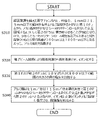
- BRIEF DESCRIPTION OF THE DRAWINGS It is a schematic diagram which shows the copper covering aluminum wire of this invention.
- BRIEF DESCRIPTION OF THE DRAWINGS It is a schematic diagram of the manufacturing apparatus which manufactures the copper coated aluminum wire of this invention. It is a flow chart which shows the process of manufacturing the copper clad aluminum wire of the present invention. It is a figure which shows typically the vapor deposition area
- FIG. 7(A) shows how the copper-coated aluminum wire is wound around the second drum
- FIG. 7(B) shows how the copper-coated aluminum wire is drawn.
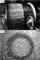
- 2 is a diagram showing SEM images of cross sections of copper-coated aluminum wires of Examples 2 and 5.
- FIG. 8A shows a cross-sectional SEM image of the copper-coated aluminum wire of Example 2
- FIG. 8B shows a cross-sectional SEM image of the copper-coated aluminum wire of Example 5.
- FIG. 2 shows the results of a scratch test of copper-coated aluminum wires of Examples 2, 5, 10, 11, 12 and 14
- FIG. 10 is a diagram showing an optical micrograph of a cross section of the copper-coated aluminum wire of Example 2 during wire drawing.
- FIG. 1 is a schematic diagram showing the copper-coated aluminum wire of the present invention.
- a copper-coated aluminum wire 100 of the present invention comprises an aluminum wire 110 made of aluminum or an aluminum alloy and a copper thin film 120 covering the aluminum wire 110 . Since the aluminum wire 110 is coated with the copper thin film 120, it has environmental resistance.
- the space factor (%) of the copper thin film 120 is 0.2% or more and 4% or less. This makes it possible to reduce the weight.
- the space factor (%) of the thin copper film 120 is the percentage of the cross-sectional area of the thin copper film 120 with respect to the total cross-sectional area of the copper-coated aluminum wire 100 .
- the space factor (%) of the copper thin film 120 is preferably in the range of 0.2% or more and less than 1%. This makes it possible to further reduce the weight.
- the space factor (%) of the copper thin film 120 is more preferably in the range of 0.3% or more and 0.55% or less. Within this range, it is possible to reduce the weight while maintaining the adhesion.
- the cross-sectional area is the area of the cross section in the direction perpendicular to the longitudinal direction of the copper-coated aluminum wire 100 .
- the copper-coated aluminum wire 100 of the present invention does not have a passive oxide film between the aluminum wire 110 and the copper thin film 120, a scratch test conforming to JIS R 3255 was performed between the aluminum wire 110 and the copper thin film 120.
- the adhesion of satisfies 10 mN or more, and does not cause poor adhesion. If it is 10 mN or more, there is no concern about adhesion failure, so the upper limit is not particularly set, but it may be 300 mN or less.
- the adhesion preferably satisfies the range of 20 mN or more and 100 mN or less. Within this range, the adhesiveness is higher, the copper thin film 120 does not peel off, and the yield strength of the copper-coated aluminum wire 100 is further improved.
- the adhesion more preferably satisfies the range of 30 mN or more and 100 mN or less, still more preferably 50 mN or more and 100 mN or less. Within this range, the yield strength of the copper-coated aluminum wire 100 is further improved.
- the aluminum wire rod 110 may be aluminum or an aluminum alloy, but aluminum preferably has a purity in the range of 99.9% or more and 99.99999% or less. With the copper-coated aluminum wire of the present invention, even a high-purity aluminum wire can be used without disconnection.
- Aluminum alloys can also be used.
- Aluminum alloys contain aluminum (Al) as main components, magnesium (Mg), iron (Fe), zirconium (Zr), zinc (Zn), chromium (Cr), An alloy with at least one element selected from the group consisting of scandium (Sc), manganese (Mn), boron (B), titanium (Ti), copper (Cu), lithium (Li) and silicon (Si) There may be.
- the content of elements other than aluminum constituting the aluminum alloy is preferably 0.1 atomic % or more and 10 atomic % or less. In this case, even if two or more elements other than Al are selected, the total content of those elements may be within the above range. From this point of view, the amount of Al, which is the main component in the aluminum alloy, may be 90 at % or more and less than 99.9 at %.
- FIG. 2 is a schematic diagram of a manufacturing apparatus for manufacturing the copper-coated aluminum wire of the present invention.
- FIG. 3 is a flow chart showing steps for manufacturing the copper-coated aluminum wire of the present invention.
- the present inventors have found that by adopting the ion plating method and setting various conditions, it is possible to remove the passive oxide film of the aluminum wire and simultaneously form an ultra-thin copper thin film.
- the method of the present invention employs the ion plating apparatus shown in FIG. 2, it should be noted that the configuration shown in FIG. 2 is an example and is not limited to this configuration.
- the ion plating apparatus 200 one having a vacuum chamber 201, an electron gun 202 provided in the vacuum chamber 201, a thermionic filament 203, and an ionization electrode 204 can be employed.
- the vacuum chamber 201 is in a state where it can be evacuated by a vacuum pump such as a diffusion pump, turbomolecular pump, or cryopump through an exhaust port.
- a vacuum pump such as a diffusion pump, turbomolecular pump, or cryopump through an exhaust port.
- a reactive gas, a discharge cleaning gas (ion bombardment processing gas), and the like are supplied to the vacuum chamber 201 through a gas supply pipe 205 .
- the electron gun 202 heats and evaporates the evaporation source (copper metal here) 207 housed in the hearth liner 206 .
- the electron gun 202 generates an electron beam 208 by power supply from an electron gun power supply (not shown) provided outside the vacuum chamber 201 .
- the electron beam 208 is deflected and hits the evaporation source within the hearth liner 206 .
- Evaporation source 207 is heated to evaporate.
- the thermionic filament 203 is connected to a filament heating power supply (not shown) and supplied with AC power.
- the thermionic filament 203 is heated by the power supply and emits thermionic electrons.
- a thermionic filament 203 is made of metal such as tungsten, molybdenum, or tantalum.
- thermoelectrons from the thermoelectron filament 203 travel toward the ionization electrode 204 and collide with evaporation particles (copper particles in this case) evaporated from the evaporation source 207 to ionize the evaporation particles.
- the ionized evaporative particles adhere to the object to form a thin film.
- a shutter 209 may be provided to control the timing of adhesion of the ionized vaporized particles to the object.
- a film thickness meter 210 may be provided so that the thickness of the formed thin film can be measured.
- Such an ion plating apparatus 200 may be similar to existing ion plating apparatuses.
- the ion plating apparatus 200 further accommodates a first drum 211 and a second drum 212 .
- An aluminum wire 110 made of aluminum or an aluminum alloy is wound around the first drum 211 , and is configured to be wound from the first drum 211 to the second drum 212 .
- a voltage can be applied to the first drum 211 and the second drum 212, so that the aluminum wire 110 becomes the object.
- the ion plating apparatus 200 further accommodates at least a pair (one set) of return rolls 213 so that the aluminum wire 110 from the first drum 211 is wound around the second drum 212 while cross-rotating. If there is a pair of return rolls, for example, a thin copper film is formed on one surface of the aluminum wire while traveling from A to B, and a thin copper film is formed on the other surface while traveling from C to D. By providing two or more pairs of return rolls, the thickness of the thin copper film covering the aluminum wire can be controlled more efficiently. 2, a combination of one return roll 213 proceeding from A to B and one return roll 213 proceeding from C to D is referred to as a pair (one set) of return rolls 213. . Therefore, as shown in FIG. 4, when there are five such combinations, it is said that five pairs (five sets) of return rolls 213 are provided.
- FIG. 2 illustrates the ion plating apparatus 200 configured such that the aluminum wire is wound from the first drum 211 to the second drum 212 via at least a pair of return rolls 213. It may be wound onto the first drum 211 via a pair of return rolls 213 .
- Each step of the method of the present invention will be explained using such an ion plating apparatus 200 .
- Step S310 Inside the vacuum chamber 201 equipped with the copper evaporation source 207, the aluminum wire 110 is removed from the first drum 211 around which the aluminum wire 110 having an outer diameter of 0.1 mm or more and 1.5 mm or less is wound. It is possible to wind on the second drum 212 by intersecting rotation (for example, in the order of A ⁇ B ⁇ C ⁇ D) via a pair of return rolls 213, and at least between the pair of return rolls 213
- the aluminum wire 110 is installed so that the distance between the aluminum wire 110 crossing over the copper evaporation source 207 and the center of the copper evaporation source 207 is 500 mm or more and 1000 mm or less. Since the aluminum wire 110 is the same as the aluminum wire described with reference to FIG. 1, the description thereof is omitted. If two pairs (two sets) or more of return rolls are provided, the number of cross rotations increases, which is advantageous for controlling the thickness of the thin copper film coated on the aluminum wire.
- step S310 when the aluminum wire 110 is set, the inside of the vacuum chamber 201 is evacuated.
- the degree of vacuum at this time is preferably in the range of 1 ⁇ 10 ⁇ 9 Pa or more and 1 ⁇ 10 ⁇ 5 Pa or less, more preferably in the range of 1 ⁇ 10 ⁇ 7 Pa or more and 1 ⁇ 10 ⁇ 5 Pa or less. be.
- FIG. 4 is a diagram schematically showing a vapor deposition area in an ion plating apparatus.
- FIG. 5 is a schematic diagram showing how a copper thin film is coated by an ion plating method.
- FIG. 4 shows an enlarged vapor deposition area in an ion plating apparatus equipped with five sets of return rolls 213 .
- a vapor deposition region 410 obtained by evaporation of the evaporation source 207 is indicated by hatching. Focusing on the evaporation area 410 that can be formed in step S320, which will be described later, there are three distances, D1, D2, and D3, between the center P of the evaporation source 207 and the aluminum wire rod 110 extending between the return rolls 213. It has length.
- the distance D1 is the shortest distance
- the distance D2 is the longest distance.
- Such distances D1, D2, and D3 each satisfy a range of 500 mm to 1000 mm, and the distances satisfy D1 ⁇ D3 ⁇ D2.
- the inventors of the present application have found that when the copper ions 520 collide with the aluminum wire 110, the passive oxide film 510 on the surface of the aluminum wire 110 is removed by the collision energy, and at the same time It was found that a copper thin film consisting of copper particles 530 was formed. From this result, it was confirmed that high adhesion between the copper thin film and the aluminum wire is possible.
- Step S320 By heating the electron beam 208, copper is evaporated from the copper evaporation source 207 and ionized. Evaporation and ionization of copper from the copper evaporation source 207 is performed by the electron gun 202 , thermionic filament 203 and the ionization electrode 204 of the ion plating apparatus 200 .
- the degree of vacuum is preferably in the range of 1 ⁇ 10 ⁇ 4 Pa or more and 1 ⁇ 10 ⁇ 2 Pa or less.
- Step S330 Apply a negative voltage in the range of greater than 10V and less than or equal to 800V to the first drum 211 and the second drum 212 .
- the positively charged copper ions ionized in step S320 can adhere to the aluminum wire 110 to which the negative voltage is applied.
- a negative voltage in the range of 50V to 700V is applied.
- the copper ions adhere to the aluminum wire 110 more efficiently.
- a negative voltage in the range of 200V to 700V is applied.
- the copper ions adhere to the aluminum wire 110 more efficiently.
- Step S340 The aluminum wire 110 is wound on the second drum 212 while being cross-rotated from the first drum 211 at a speed of 1 m/min or more and less than 15 m/min via at least one pair of return rolls 213, and the ionized copper is A copper thin film is formed by bombarding the aluminum wire with ions. As a result, a copper thin film is formed on the surface of the aluminum wire 110 while destroying and removing the passive oxide film on the surface of the aluminum wire 110, so that the copper-coated aluminum wire 100 (FIG. 1) is obtained. If the winding speed is lower than 1 m/min, the temperature of the aluminum wire increases due to collisions with copper ions, and there is a risk that the aluminum wire will break during the ion plating process. If the winding speed is 15 m/min or more, there may be areas where the aluminum wire is not coated with copper.
- the aluminum wire 100 is wound at a speed of 1 m/min or more and 5 m/min or less. As a result, a copper-coated aluminum wire from which the passivation oxide film has been removed can be efficiently obtained.
- the aluminum wire 100 is wound at a speed of 2 m/min or more and 5 m/min or less. Thereby, a copper-coated aluminum wire having no passivation oxide film can be obtained more efficiently.
- step S330 may be repeated. For example, after winding the aluminum wire 100 from the first drum 211 to the second drum 212, the second drum 212 is replaced with the first drum 211, and the first drum is replaced with the second drum 212. , step S330 may be performed again. Thereby, the thickness of the thin copper film covering the aluminum wire can be controlled. Alternatively, after winding the aluminum wire 100 from the first drum 211 to the second drum 212 , the aluminum wire 110 from the second drum 212 is cross-rotated via at least one pair of return rolls 213 while being wound around the first drum. 211, step S330 may be performed in the reverse direction (for example, D->C->B->A in FIG.
- step S330 may be step S330.
- the copper thin film having a thickness according to the application can be applied to the aluminum wire rod 110 more efficiently. can be coated on
- Steps S320, S330 and S340 may be performed simultaneously, or step S340 and then steps S320 and S330 may be performed in this order.
- ion bombardment treatment using argon ions may be performed to clean the surface of the aluminum wire 110 .
- the first drum 211 and the second drum 212 are cross-rotated via at least one pair of return rolls 213 while a negative voltage is applied to the first drum 211 and the second drum 212 .
- the aluminum wire rod 110 may be wound on the second drum 212 while the aluminum wire rod 110 is being wound. Thereby, the surface of the aluminum wire 110 can be cleaned.
- the degree of vacuum is preferably in the range of 1 Pa or more and 10 Pa or less. This promotes the generation of argon plasma more efficiently.
- the degree of vacuum is again set to the range of 1 ⁇ 10 ⁇ 9 Pa or more and 1 ⁇ 10 ⁇ 5 Pa or less, more preferably 1 ⁇ 10 ⁇ 7 Pa or more and 1 ⁇ 10 ⁇ 5 Pa or less.
- step S320 may be implemented.
- the winding speed is not particularly limited, but may be, for example, 5 m/min or more and 15 m/min.
- a negative voltage in the range of 100 V to 400 V may be applied to the first drum 211 and the second drum 212 . This promotes cleaning with argon plasma more efficiently.
- FIG. 6 is a diagram schematically showing the wire drawing process.
- the obtained copper-coated aluminum wire 100 may be further subjected to wire drawing.
- a high-purity soft aluminum wire 110 can be coated with a copper thin film, so that the overall yield strength of the obtained copper-coated aluminum wire 100 is increased. Therefore, even the high-purity aluminum wire 110 can be made into an ultra-thin wire by wire drawing.
- Such a wire drawing process is not particularly limited, but is preferably a drawing process using a cemented carbide die or a diamond die as shown in FIG.
- the aluminum wire 110 having an outer diameter in the range of 0.1 mm or more and 1.5 mm or less can be ultrathin to an outer diameter in the range of 0.05 mm or more and less than 0.1 mm.
- the copper-coated aluminum wire 100 Before, after, or during drawing, the copper-coated aluminum wire 100 may be annealed in a temperature range of 300°C to 500°C for 1 second to 5 minutes. As a result, the strain generated during the drawing process is removed, so cracks and micro-cracks in the aluminum wire rod 110 can be suppressed more efficiently.
- the drawing and annealing may be performed multiple times until the desired outer diameter is achieved, as shown in FIG.
- Examples 1 to 24 Using an ion plating apparatus 200 (FIG. 2) equipped with five sets of return rolls 213 (FIG. 4) and housing a copper evaporation source 207 (FIG. 2) (copper purity 99.999%), An aluminum wire 110 (FIG. 1) made of aluminum or an aluminum alloy was coated with a copper thin film to produce a copper-coated aluminum wire.
- Aluminum wires were installed in the vacuum chamber 201 (FIG. 2) so that the distances D1, D2 and D3 were 500 mm, 1000 mm and 700 mm, respectively, as shown in FIG. 4 (step S310 in FIG. 3).
- the aluminum wire (FIG. 1) is wound around the first drum 211 (FIG. 2), and the aluminum wire is passed through five pairs of return rolls 410 so as to rotate 10 times so as to be wound on the second drum. 212 (FIG. 2), and the distance between the aluminum wire 110 passing between the five sets of return rolls 213 and the center P of the copper evaporation source 207 satisfies the range of 500 mm or more and 1000 mm or less. It was installed so as to form a structure.
- the vacuum chamber 201 was evacuated by a vacuum pump so that the degree of vacuum in the vacuum chamber 201 was 1 ⁇ 10 ⁇ 6 Pa.
- argon gas was introduced into the vacuum chamber 201 so that the pressure was in the range of 1 Pa or more and 10 Pa or less.
- a negative voltage of 240 V was applied to the first drum 211 and the second drum 212 to generate argon plasma.
- the aluminum wire was wound (rewound) from the first drum 211 to the second drum 212 via five sets of return rolls. At this time, the rewinding speed of the aluminum wire was set to 10 m/min.
- the copper evaporation source 207 was evaporated and ionized by heating with the electron beam 208 (step S320 in FIG. 3). Specifically, the thermoelectron voltage is 14 V, the thermoelectron current is 80 A, the emission current is 450 mA, the ionization voltage is 50 V, and the ionization current is 90 A. The degree of vacuum in the vacuum chamber 201 is 1 ⁇ 10 ⁇ 3 Pa, and the amount of copper evaporation is controlled. .
- a negative voltage having the magnitude shown in Table 1 was applied to the first drum 211 and the second drum 212 (step S330 in FIG. 3).
- the aluminum wire 110 was wound around the second drum 212 while being cross-rotated 10 times from the first drum 211 through five sets of return rolls 213 at the speed shown in Table 1, and the ionized copper ions were transferred to the aluminum wire 110. Collisions were made to form a copper thin film (step S340 in FIG. 3).
- the formation of copper thin films was repeated.
- the repetition number of 0 means that the formation of the copper thin film (step S340 in FIG. 3) was performed once, and the repetition number of 1 means that the copper thin film was formed twice.
- the repetition of the formation of the copper thin film was performed in detail as follows.
- the electron beam heating and voltage application to the first drum 211 and the second drum 212 were stopped, and the degree of vacuum in the vacuum chamber 201 was evacuated to 1 ⁇ 10 ⁇ 6 Pa. .
- the second drum 212 is rewound onto the first drum 211, again subjected to electron beam heating under the above conditions, a negative voltage is applied, and the copper thin film is wound at the speed shown in Table 1. formed.
- wire drawing was applied to some examples.
- the wire drawing process was a drawing process using a diamond die multiple times, as shown in FIG. Annealing treatment was performed at 300° C. for 30 seconds after drawing.
- FIG. 7 is a diagram showing the appearance of the copper-coated aluminum wire of Example 2.
- FIG. 7(A) shows how the copper-coated aluminum wire is wound around the second drum 212
- FIG. 7(B) shows how the copper-coated aluminum wire is drawn. Although shown in gray scale in FIG. 7, the surface of the wire showed the luster of copper in each case.
- FIG. 8 is a diagram showing SEM images of cross sections of the copper-coated aluminum wires of Examples 2 and 5.
- FIG. 8(A) is a cross-sectional SEM image of the copper-coated aluminum wire of Example 2
- FIG. 8(B) is a cross-sectional SEM image of the copper-coated aluminum wire of Example 5.
- FIG. 8(A) it was found that there was no passive oxide film at the interface between the aluminum wire and the copper thin film.
- FIG. 8B a passive oxide film with a thickness of about 10 nm was observed at the interface between the aluminum wire and the copper thin film.
- a passive oxide film was formed at the interface between the aluminum wire and the copper thin film. was not seen.
- the method of the present invention is a suitable method for covering a copper thin film while removing the passive oxide film on the surface of the aluminum wire, and high adhesion between the aluminum wire and the copper thin film can be obtained. It was shown that
- the space factor of the copper thin film was 0.2. % or more and 4% or less, preferably 0.3% or more and 0.55% or less
- the adhesion between the aluminum wire and the copper thin film based on the scratch test in accordance with JIS R 3255 is 10 mN or more. , preferably 20 mN or more and 100 mN or less, more preferably 30 mN or more and 100 mN or less, and even more preferably 50 mN or more and 100 mN or less, a copper-coated aluminum wire can be obtained.
- FIG. 9 is a diagram showing the results of a scratch test of the copper-coated aluminum wires of Examples 2, 5, 10, 11, 12 and 14.
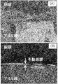
- FIG. 10 is a diagram showing an optical microscope photograph of a cross section of the copper-coated aluminum wire of Example 2 during wire drawing.
- Fig. 10 shows changes in the cross section of the copper-coated aluminum wire rod of Example 2 during the drawing process, and the outer diameters were 1.004 mm, 0.920 mm, and 0.837 mm from the left. It was confirmed that the copper thin film was firmly adhered without peeling off even when the drawing process was performed multiple times using a die.
- a copper-coated aluminum wire with excellent adhesion and reduced weight is provided, so it can be applied to wires such as electronic devices, cable conductors, braided wires, and coils for various motors.
- REFERENCE SIGNS LIST 100 copper-coated aluminum wire 110 aluminum wire 120 copper thin film 200 ion plating device 201 vacuum chamber 202 electron gun 203 thermionic filament 204 ionization electrode 205 gas supply pipe 206 hearth liner 207 evaporation source 208 electron beam 209 shutter 210 film thickness gauge 211 first drum 212 second drum 213 return roll 410 deposition zone 510 passive oxide film 520 copper ions 530 copper particles
Landscapes
- Chemical & Material Sciences (AREA)
- Metallurgy (AREA)
- Chemical Kinetics & Catalysis (AREA)
- Engineering & Computer Science (AREA)
- Materials Engineering (AREA)
- Mechanical Engineering (AREA)
- Organic Chemistry (AREA)
- Inorganic Chemistry (AREA)
- Physics & Mathematics (AREA)
- Thermal Sciences (AREA)
- Health & Medical Sciences (AREA)
- Toxicology (AREA)
- General Chemical & Material Sciences (AREA)
- Physical Vapour Deposition (AREA)
Abstract
Description
前記銅薄膜の占積率は、0.2%以上1%未満の範囲であってもよい。
前記銅薄膜の占積率は、0.3%以上0.55%以下の範囲であってもよい。
前記密着性は、20mN以上100mN以下の範囲を満たしてもよい。
前記密着性は、50mN以上100mN以下の範囲を満たしてもよい。
前記アルミニウムは、99.9%以上99.99999%以下の範囲の純度を有してもよい。
前記アルミニウム合金は、アルミニウム(Al)と、マグネシウム(Mg)、鉄(Fe)、ジルコニウム(Zr)、亜鉛(Zn)、クロム(Cr)、スカンジウム(Sc)、マンガン(Mn)、ホウ素(B)、チタン(Ti)、銅(Cu)、リチウム(Li)およびケイ素(Si)からなる群から選択される少なくとも1種の元素との合金であってもよい。
前記アルミ線材と前記銅薄膜との界面に不働態酸化被膜を有しなくてもよい。
本発明によるアルミニウムまたはアルミニウム合金からなるアルミ線材にイオンプレーティング法により銅薄膜を被覆し、銅被覆アルミニウム線材を製造する方法は、銅蒸発源を備えた真空チャンバ内に、外径0.1mm以上1.5mm以下の範囲を有するアルミ線材が巻回された第1のドラムから、前記アルミ線材が少なくとも一対のリターンロールを介して交差回転するようにして第2のドラムに巻き取らせることが可能となり、かつ、前記少なくとも一対のリターンロール間を渡る前記アルミ線材と前記銅蒸発源の中心との間の距離が500mm以上1000mm以下となるように、前記アルミ線材を設置することと、電子ビーム加熱により前記銅蒸発源から銅を蒸発させ、イオン化することと、前記第1のドラムおよび前記第2のドラムに10Vより大きく800V以下の範囲の大きさの負の電圧を印加することと、前記アルミ線材を1m/分以上15m/分未満の速度で前記第1のドラムから前記少なくとも一対のリターンロールを介して交差回転させながら前記第2のドラムに巻き取らせ、イオン化した銅イオンを前記アルミ線材に衝突させ、銅薄膜を形成することとを包含し、これにより上記課題を解決する。
前記負の電圧を印加することは、50V以上700V以下の範囲の大きさの負の電圧を印加してもよい。
前記負の電圧を印加することは、200V以上700V以下の範囲の大きさの負の電圧を印加してもよい。
前記銅薄膜を形成することは、前記アルミ線を1m/分以上5m/分以下の速度で巻き取らせてもよい。
前記アルミニウムは、99.9%以上99.99999%以下の範囲の純度を有してもよい。
前記アルミニウム合金は、アルミニウム(Al)と、マグネシウム(Mg)、鉄(Fe)、ジルコニウム(Zr)、亜鉛(Zn)、クロム(Cr)、スカンジウム(Sc)、マンガン(Mn)、ホウ素(B)、チタン(Ti)、銅(Cu)、リチウム(Li)およびケイ素(Si)からなる群から選択される少なくとも1種の元素との合金であってもよい。
前記銅を蒸発させ、イオン化することに先立って、アルゴンイオンを用いたイオンボンバードメント処理によって前記アルミ線の表面を洗浄することをさらに包含してもよい。
前記イオンボンバードメント処理は、1Pa以上10Pa以下の範囲の真空チャンバ内の圧力で行ってもよい。
前記銅薄膜を形成することを繰り返すことをさらに包含してもよい。
前記銅薄膜を形成することによって得られた銅被覆アルミニウム線材を伸線処理することをさらに包含してもよい。
前記伸線処理は、超硬ダイスまたはダイヤモンドダイスを用いた引き抜き加工であってもよい。
前記引き抜き加工の前、後または時に、前記銅被覆アルミニウム線材を300℃以上500℃以下の温度範囲で1秒以上5分以下の時間、焼鈍してもよい。
図3は、本発明の銅被覆アルミニウム線材を製造する工程を示すフローチャートである。
図5は、イオンプレーティング法による銅薄膜が被覆される様子を示す模式図である。
5組のリターンロール213(図4)を備え、銅蒸発源207(図2)(銅の純度99.999%)を収容したイオンプレーティング装置200(図2)を用いて、表1に示すアルミニウムまたはアルミニウム合金からなるアルミ線材110(図1)に銅薄膜を被覆し、銅被覆アルミニウム線材を製造した。


110 アルミ線材
120 銅薄膜
200 イオンプレーティング装置
201 真空チャンバ
202 電子銃
203 熱電子フィラメント
204 イオン化電極
205 ガス供給管
206 ハースライナ
207 蒸発源
208 電子ビーム
209 シャッタ
210 膜厚計
211 第1のドラム
212 第2のドラム
213 リターンロール
410 蒸着領域
510 不働態酸化被膜
520 銅イオン
530 銅粒子
Claims (20)
- アルミニウムまたはアルミニウム合金からなるアルミ線材と、
前記アルミ線材を被覆する銅薄膜と
を備え、
銅薄膜の占積率は、0.2%以上4%以下の範囲であり、
JIS R 3255に準拠したスクラッチ試験に基づく前記アルミ線材と前記銅薄膜との間の密着性は、10mN以上を満たす、銅被覆アルミニウム線材。 - 前記銅薄膜の占積率は、0.2%以上1%未満の範囲である、請求項1に記載の銅被覆アルミニウム線材。
- 前記銅薄膜の占積率は、0.3%以上0.55%以下の範囲である、請求項2に記載の銅被覆アルミニウム線材。
- 前記密着性は、20mN以上100mN以下の範囲を満たす、請求項1~3のいずれかに記載の銅被覆アルミニウム線材。
- 前記密着性は、50mN以上100mN以下の範囲を満たす、請求項4に記載の銅被覆アルミニウム線材。
- 前記アルミニウムは、99.9%以上99.99999%以下の範囲の純度を有する、請求項1~5のいずれかに記載の銅被覆アルミニウム線材。
- 前記アルミニウム合金は、アルミニウム(Al)と、マグネシウム(Mg)、鉄(Fe)、ジルコニウム(Zr)、亜鉛(Zn)、クロム(Cr)、スカンジウム(Sc)、マンガン(Mn)、ホウ素(B)、チタン(Ti)、銅(Cu)、リチウム(Li)およびケイ素(Si)からなる群から選択される少なくとも1種の元素との合金である、請求項1~5のいずれかに記載の銅被覆アルミニウム線材。
- 前記アルミ線材と前記銅薄膜との界面に不働態酸化被膜を有しない、請求項1~7のいずれかに記載の銅被覆アルミニウム線材。
- アルミニウムまたはアルミニウム合金からなるアルミ線材にイオンプレーティング法により銅薄膜を被覆し、銅被覆アルミニウム線材を製造する方法であって、
銅蒸発源を備えた真空チャンバ内に、外径0.1mm以上1.5mm以下の範囲を有するアルミ線材が巻回された第1のドラムから、前記アルミ線材が少なくとも一対のリターンロールを介して交差回転するようにして第2のドラムに巻き取らせることが可能となり、かつ、前記少なくとも一対のリターンロール間を渡る前記アルミ線材と前記銅蒸発源の中心との間の距離が500mm以上1000mm以下となるように、前記アルミ線材を設置することと、
電子ビーム加熱により前記銅蒸発源から銅を蒸発させ、イオン化することと、
前記第1のドラムおよび前記第2のドラムに10Vより大きく800V以下の範囲の大きさの負の電圧を印加することと、
前記アルミ線材を1m/分以上15m/分未満の速度で前記第1のドラムから前記少なくとも一対のリターンロールを介して交差回転させながら前記第2のドラムに巻き取らせ、イオン化した銅イオンを前記アルミ線材に衝突させ、銅薄膜を形成することと
を包含する、方法。 - 前記負の電圧を印加することは、50V以上700V以下の範囲の大きさの負の電圧を印加することである、請求項9に記載の方法。
- 前記負の電圧を印加することは、200V以上700V以下の範囲の大きさの負の電圧を印加することである、請求項10に記載の方法。
- 前記銅薄膜を形成することは、前記アルミ線を1m/分以上5m/分以下の速度で巻き取らせることである、請求項9~11のいずれかに記載の方法。
- 前記アルミニウムは、99.9%以上99.99999%以下の範囲の純度を有する、請求項8~12のいずれかに記載の方法。
- 前記アルミニウム合金は、アルミニウム(Al)と、マグネシウム(Mg)、鉄(Fe)、ジルコニウム(Zr)、亜鉛(Zn)、クロム(Cr)、スカンジウム(Sc)、マンガン(Mn)、ホウ素(B)、チタン(Ti)、銅(Cu)、リチウム(Li)およびケイ素(Si)からなる群から選択される少なくとも1種の元素との合金である、請求項9~12のいずれかに記載の方法。
- 前記銅を蒸発させ、イオン化することに先立って、アルゴンイオンを用いたイオンボンバードメント処理によって前記アルミ線の表面を洗浄することをさらに包含する、請求項9~14のいずれかに記載の方法。
- 前記イオンボンバードメント処理は、1Pa以上10Pa以下の範囲の真空チャンバ内の圧力で行う、請求項15に記載の方法。
- 前記銅薄膜を形成することを繰り返すことをさらに包含する、請求項9~16のいずれかに記載の方法。
- 前記銅薄膜を形成することによって得られた銅被覆アルミニウム線材を伸線処理することをさらに包含する、請求項9~17のいずれかに記載の方法。
- 前記伸線処理は、超硬ダイスまたはダイヤモンドダイスを用いた引き抜き加工である、請求項18に記載の方法。
- 前記引き抜き加工の前、後または時に、前記銅被覆アルミニウム線材を300℃以上500℃以下の温度範囲で1秒以上5分以下の時間、焼鈍する、請求項19に記載の方法。
Priority Applications (3)
| Application Number | Priority Date | Filing Date | Title |
|---|---|---|---|
| EP22766901.7A EP4306673A1 (en) | 2021-03-12 | 2022-02-28 | Copper-coated aluminum wire material and production method therefor |
| JP2023505312A JPWO2022190942A1 (ja) | 2021-03-12 | 2022-02-28 | |
| US18/275,775 US20240117483A1 (en) | 2021-03-12 | 2022-02-28 | Copper-Coated Aluminum Wire Material and Production Method Therefor |
Applications Claiming Priority (2)
| Application Number | Priority Date | Filing Date | Title |
|---|---|---|---|
| JP2021-040009 | 2021-03-12 | ||
| JP2021040009 | 2021-03-12 |
Publications (1)
| Publication Number | Publication Date |
|---|---|
| WO2022190942A1 true WO2022190942A1 (ja) | 2022-09-15 |
Family
ID=83226786
Family Applications (1)
| Application Number | Title | Priority Date | Filing Date |
|---|---|---|---|
| PCT/JP2022/008429 WO2022190942A1 (ja) | 2021-03-12 | 2022-02-28 | 銅被覆アルミニウム線材およびその製造方法 |
Country Status (4)
| Country | Link |
|---|---|
| US (1) | US20240117483A1 (ja) |
| EP (1) | EP4306673A1 (ja) |
| JP (1) | JPWO2022190942A1 (ja) |
| WO (1) | WO2022190942A1 (ja) |
Citations (4)
| Publication number | Priority date | Publication date | Assignee | Title |
|---|---|---|---|---|
| JPS621850A (ja) * | 1985-06-26 | 1987-01-07 | Sumitomo Electric Ind Ltd | 複合線状体の製造方法およびその装置 |
| JPH05285690A (ja) * | 1992-04-15 | 1993-11-02 | Sumitomo Electric Ind Ltd | 溶接用複合材およびその製造方法 |
| JP2005248318A (ja) * | 2004-02-06 | 2005-09-15 | Kansai Engineering:Kk | 音響用、ic用、キーレスエントリーシステム用、ミニチュアモーター巻線用、スピーカーボイスコイル用、送電線用、及び電機部品用線材 |
| WO2019193960A1 (ja) * | 2018-04-06 | 2019-10-10 | 古河電気工業株式会社 | めっき線棒 |
-
2022
- 2022-02-28 WO PCT/JP2022/008429 patent/WO2022190942A1/ja active Application Filing
- 2022-02-28 US US18/275,775 patent/US20240117483A1/en active Pending
- 2022-02-28 EP EP22766901.7A patent/EP4306673A1/en active Pending
- 2022-02-28 JP JP2023505312A patent/JPWO2022190942A1/ja active Pending
Patent Citations (4)
| Publication number | Priority date | Publication date | Assignee | Title |
|---|---|---|---|---|
| JPS621850A (ja) * | 1985-06-26 | 1987-01-07 | Sumitomo Electric Ind Ltd | 複合線状体の製造方法およびその装置 |
| JPH05285690A (ja) * | 1992-04-15 | 1993-11-02 | Sumitomo Electric Ind Ltd | 溶接用複合材およびその製造方法 |
| JP2005248318A (ja) * | 2004-02-06 | 2005-09-15 | Kansai Engineering:Kk | 音響用、ic用、キーレスエントリーシステム用、ミニチュアモーター巻線用、スピーカーボイスコイル用、送電線用、及び電機部品用線材 |
| WO2019193960A1 (ja) * | 2018-04-06 | 2019-10-10 | 古河電気工業株式会社 | めっき線棒 |
Also Published As
| Publication number | Publication date |
|---|---|
| JPWO2022190942A1 (ja) | 2022-09-15 |
| EP4306673A1 (en) | 2024-01-17 |
| US20240117483A1 (en) | 2024-04-11 |
Similar Documents
| Publication | Publication Date | Title |
|---|---|---|
| CN101401186B (zh) | X-射线电子管的改良阴极结构 | |
| CN1727179B (zh) | 多层金属复合薄膜及其制造方法 | |
| CN102634761B (zh) | 截面为带状的真空阴极电弧等离子体的磁过滤方法 | |
| JP2008258581A (ja) | プラスチック基板を堆積するためのデバイスおよびプロセス | |
| WO2022190942A1 (ja) | 銅被覆アルミニウム線材およびその製造方法 | |
| JP2005054259A (ja) | プラスチックフィルム及びその製造方法及びそれを応用したフレキシブルプリント回路基板 | |
| KR100757736B1 (ko) | 플라즈마 이온주입 및 증착법을 이용한 fccl 제조장치 | |
| WO2020093375A1 (zh) | 膜及制备工艺 | |
| JPWO2022190942A5 (ja) | ||
| US4901338A (en) | Rotary anode for X-ray tubes and method of manufacture | |
| RU2407820C1 (ru) | Способ нанесения покрытия на изделия из керамики в вакууме | |
| JP7191937B2 (ja) | 導電性フィルムの製造方法 | |
| JP2007297712A (ja) | プラズマを利用して堆積された薄いシード層を介してのメタライゼーション | |
| TW200814129A (en) | Electrode for cold cathode fluorescent lamp | |
| JPH1192920A (ja) | 金属パイプの内側コーティング方法とその方法を実施する装置 | |
| JP2005191276A (ja) | 希土類系永久磁石に対する耐塩水性付与方法および耐塩水性に優れた希土類系永久磁石 | |
| CN108008476A (zh) | 一种激光发生器反射板 | |
| US20150156887A1 (en) | Method of forming amorphous alloy film and printed wiring board manufactured by the same | |
| JP2008297174A (ja) | カーボンナノチューブ成長用基板の製造方法 | |
| JP2011046982A (ja) | 表面処理された化成処理鋼板の製造方法 | |
| JP7341919B2 (ja) | 電縫鋼管の溶接ビード切削部の補修方法、及び電縫鋼管の製造方法 | |
| CN114032513A (zh) | 一种基于磁过滤阴极真空弧法制备焊丝涂层的方法 | |
| JP3078602B2 (ja) | Hcd型イオンプレーティング装置 | |
| EP3249072B1 (en) | Method for increasing the electrical conductivity of a composite part surface | |
| US20120241184A1 (en) | Device housing and method for making same |
Legal Events
| Date | Code | Title | Description |
|---|---|---|---|
| 121 | Ep: the epo has been informed by wipo that ep was designated in this application |
Ref document number: 22766901 Country of ref document: EP Kind code of ref document: A1 |
|
| ENP | Entry into the national phase |
Ref document number: 2023505312 Country of ref document: JP Kind code of ref document: A |
|
| WWE | Wipo information: entry into national phase |
Ref document number: 18275775 Country of ref document: US |
|
| WWE | Wipo information: entry into national phase |
Ref document number: 2022766901 Country of ref document: EP |
|
| NENP | Non-entry into the national phase |
Ref country code: DE |
|
| ENP | Entry into the national phase |
Ref document number: 2022766901 Country of ref document: EP Effective date: 20231012 |