WO2022190694A1 - 基板、基板の製造方法、及び単位セルの製造方法 - Google Patents
基板、基板の製造方法、及び単位セルの製造方法 Download PDFInfo
- Publication number
- WO2022190694A1 WO2022190694A1 PCT/JP2022/003180 JP2022003180W WO2022190694A1 WO 2022190694 A1 WO2022190694 A1 WO 2022190694A1 JP 2022003180 W JP2022003180 W JP 2022003180W WO 2022190694 A1 WO2022190694 A1 WO 2022190694A1
- Authority
- WO
- WIPO (PCT)
- Prior art keywords
- substrate
- alkali metal
- metal azide
- spots
- azide
- Prior art date
- Legal status (The legal status is an assumption and is not a legal conclusion. Google has not performed a legal analysis and makes no representation as to the accuracy of the status listed.)
- Ceased
Links
Images


Classifications
-
- C—CHEMISTRY; METALLURGY
- C03—GLASS; MINERAL OR SLAG WOOL
- C03C—CHEMICAL COMPOSITION OF GLASSES, GLAZES OR VITREOUS ENAMELS; SURFACE TREATMENT OF GLASS; SURFACE TREATMENT OF FIBRES OR FILAMENTS MADE FROM GLASS, MINERALS OR SLAGS; JOINING GLASS TO GLASS OR OTHER MATERIALS
- C03C17/00—Surface treatment of glass, not in the form of fibres or filaments, by coating
- C03C17/22—Surface treatment of glass, not in the form of fibres or filaments, by coating with other inorganic material
-
- G—PHYSICS
- G04—HOROLOGY
- G04F—TIME-INTERVAL MEASURING
- G04F5/00—Apparatus for producing preselected time intervals for use as timing standards
- G04F5/14—Apparatus for producing preselected time intervals for use as timing standards using atomic clocks
-
- B—PERFORMING OPERATIONS; TRANSPORTING
- B32—LAYERED PRODUCTS
- B32B—LAYERED PRODUCTS, i.e. PRODUCTS BUILT-UP OF STRATA OF FLAT OR NON-FLAT, e.g. CELLULAR OR HONEYCOMB, FORM
- B32B17/00—Layered products essentially comprising sheet glass, or glass, slag, or like fibres
- B32B17/06—Layered products essentially comprising sheet glass, or glass, slag, or like fibres comprising glass as the main or only constituent of a layer, next to another layer of a specific material
- B32B17/10—Layered products essentially comprising sheet glass, or glass, slag, or like fibres comprising glass as the main or only constituent of a layer, next to another layer of a specific material of synthetic resin
-
- B—PERFORMING OPERATIONS; TRANSPORTING
- B32—LAYERED PRODUCTS
- B32B—LAYERED PRODUCTS, i.e. PRODUCTS BUILT-UP OF STRATA OF FLAT OR NON-FLAT, e.g. CELLULAR OR HONEYCOMB, FORM
- B32B27/00—Layered products comprising a layer of synthetic resin
- B32B27/28—Layered products comprising a layer of synthetic resin comprising synthetic resins not wholly covered by any one of the sub-groups B32B27/30 - B32B27/42
- B32B27/283—Layered products comprising a layer of synthetic resin comprising synthetic resins not wholly covered by any one of the sub-groups B32B27/30 - B32B27/42 comprising polysiloxanes
-
- B—PERFORMING OPERATIONS; TRANSPORTING
- B32—LAYERED PRODUCTS
- B32B—LAYERED PRODUCTS, i.e. PRODUCTS BUILT-UP OF STRATA OF FLAT OR NON-FLAT, e.g. CELLULAR OR HONEYCOMB, FORM
- B32B3/00—Layered products comprising a layer with external or internal discontinuities or unevennesses, or a layer of non-planar shape; Layered products comprising a layer having particular features of form
- B32B3/26—Layered products comprising a layer with external or internal discontinuities or unevennesses, or a layer of non-planar shape; Layered products comprising a layer having particular features of form characterised by a particular shape of the outline of the cross-section of a continuous layer; characterised by a layer with cavities or internal voids ; characterised by an apertured layer
- B32B3/266—Layered products comprising a layer with external or internal discontinuities or unevennesses, or a layer of non-planar shape; Layered products comprising a layer having particular features of form characterised by a particular shape of the outline of the cross-section of a continuous layer; characterised by a layer with cavities or internal voids ; characterised by an apertured layer characterised by an apertured layer, the apertures going through the whole thickness of the layer, e.g. expanded metal, perforated layer, slit layer regular cells B32B3/12
-
- B—PERFORMING OPERATIONS; TRANSPORTING
- B32—LAYERED PRODUCTS
- B32B—LAYERED PRODUCTS, i.e. PRODUCTS BUILT-UP OF STRATA OF FLAT OR NON-FLAT, e.g. CELLULAR OR HONEYCOMB, FORM
- B32B3/00—Layered products comprising a layer with external or internal discontinuities or unevennesses, or a layer of non-planar shape; Layered products comprising a layer having particular features of form
- B32B3/26—Layered products comprising a layer with external or internal discontinuities or unevennesses, or a layer of non-planar shape; Layered products comprising a layer having particular features of form characterised by a particular shape of the outline of the cross-section of a continuous layer; characterised by a layer with cavities or internal voids ; characterised by an apertured layer
- B32B3/30—Layered products comprising a layer with external or internal discontinuities or unevennesses, or a layer of non-planar shape; Layered products comprising a layer having particular features of form characterised by a particular shape of the outline of the cross-section of a continuous layer; characterised by a layer with cavities or internal voids ; characterised by an apertured layer characterised by a layer formed with recesses or projections, e.g. hollows, grooves, protuberances, ribs
-
- B—PERFORMING OPERATIONS; TRANSPORTING
- B32—LAYERED PRODUCTS
- B32B—LAYERED PRODUCTS, i.e. PRODUCTS BUILT-UP OF STRATA OF FLAT OR NON-FLAT, e.g. CELLULAR OR HONEYCOMB, FORM
- B32B37/00—Methods or apparatus for laminating, e.g. by curing or by ultrasonic bonding
- B32B37/14—Methods or apparatus for laminating, e.g. by curing or by ultrasonic bonding characterised by the properties of the layers
- B32B37/16—Methods or apparatus for laminating, e.g. by curing or by ultrasonic bonding characterised by the properties of the layers with all layers existing as coherent layers before laminating
- B32B37/18—Methods or apparatus for laminating, e.g. by curing or by ultrasonic bonding characterised by the properties of the layers with all layers existing as coherent layers before laminating involving the assembly of discrete sheets or panels only
- B32B37/182—Methods or apparatus for laminating, e.g. by curing or by ultrasonic bonding characterised by the properties of the layers with all layers existing as coherent layers before laminating involving the assembly of discrete sheets or panels only one or more of the layers being plastic
-
- B—PERFORMING OPERATIONS; TRANSPORTING
- B32—LAYERED PRODUCTS
- B32B—LAYERED PRODUCTS, i.e. PRODUCTS BUILT-UP OF STRATA OF FLAT OR NON-FLAT, e.g. CELLULAR OR HONEYCOMB, FORM
- B32B38/00—Ancillary operations in connection with laminating processes
- B32B38/0004—Cutting, tearing or severing, e.g. bursting; Cutter details
-
- B—PERFORMING OPERATIONS; TRANSPORTING
- B32—LAYERED PRODUCTS
- B32B—LAYERED PRODUCTS, i.e. PRODUCTS BUILT-UP OF STRATA OF FLAT OR NON-FLAT, e.g. CELLULAR OR HONEYCOMB, FORM
- B32B38/00—Ancillary operations in connection with laminating processes
- B32B38/0008—Electrical discharge treatment, e.g. corona, plasma treatment; wave energy or particle radiation
-
- G—PHYSICS
- G04—HOROLOGY
- G04F—TIME-INTERVAL MEASURING
- G04F5/00—Apparatus for producing preselected time intervals for use as timing standards
- G04F5/14—Apparatus for producing preselected time intervals for use as timing standards using atomic clocks
- G04F5/145—Apparatus for producing preselected time intervals for use as timing standards using atomic clocks using Coherent Population Trapping
-
- H—ELECTRICITY
- H03—ELECTRONIC CIRCUITRY
- H03L—AUTOMATIC CONTROL, STARTING, SYNCHRONISATION OR STABILISATION OF GENERATORS OF ELECTRONIC OSCILLATIONS OR PULSES
- H03L7/00—Automatic control of frequency or phase; Synchronisation
- H03L7/26—Automatic control of frequency or phase; Synchronisation using energy levels of molecules, atoms, or subatomic particles as a frequency reference
-
- B—PERFORMING OPERATIONS; TRANSPORTING
- B32—LAYERED PRODUCTS
- B32B—LAYERED PRODUCTS, i.e. PRODUCTS BUILT-UP OF STRATA OF FLAT OR NON-FLAT, e.g. CELLULAR OR HONEYCOMB, FORM
- B32B2250/00—Layers arrangement
- B32B2250/03—3 layers
-
- B—PERFORMING OPERATIONS; TRANSPORTING
- B32—LAYERED PRODUCTS
- B32B—LAYERED PRODUCTS, i.e. PRODUCTS BUILT-UP OF STRATA OF FLAT OR NON-FLAT, e.g. CELLULAR OR HONEYCOMB, FORM
- B32B2250/00—Layers arrangement
- B32B2250/40—Symmetrical or sandwich layers, e.g. ABA, ABCBA, ABCCBA
-
- B—PERFORMING OPERATIONS; TRANSPORTING
- B32—LAYERED PRODUCTS
- B32B—LAYERED PRODUCTS, i.e. PRODUCTS BUILT-UP OF STRATA OF FLAT OR NON-FLAT, e.g. CELLULAR OR HONEYCOMB, FORM
- B32B2255/00—Coating on the layer surface
- B32B2255/20—Inorganic coating
-
- B—PERFORMING OPERATIONS; TRANSPORTING
- B32—LAYERED PRODUCTS
- B32B—LAYERED PRODUCTS, i.e. PRODUCTS BUILT-UP OF STRATA OF FLAT OR NON-FLAT, e.g. CELLULAR OR HONEYCOMB, FORM
- B32B2310/00—Treatment by energy or chemical effects
- B32B2310/08—Treatment by energy or chemical effects by wave energy or particle radiation
- B32B2310/0806—Treatment by energy or chemical effects by wave energy or particle radiation using electromagnetic radiation
- B32B2310/0831—Treatment by energy or chemical effects by wave energy or particle radiation using electromagnetic radiation using UV radiation
-
- B—PERFORMING OPERATIONS; TRANSPORTING
- B32—LAYERED PRODUCTS
- B32B—LAYERED PRODUCTS, i.e. PRODUCTS BUILT-UP OF STRATA OF FLAT OR NON-FLAT, e.g. CELLULAR OR HONEYCOMB, FORM
- B32B2315/00—Other materials containing non-metallic inorganic compounds not provided for in groups B32B2311/00 - B32B2313/04
- B32B2315/08—Glass
-
- B—PERFORMING OPERATIONS; TRANSPORTING
- B32—LAYERED PRODUCTS
- B32B—LAYERED PRODUCTS, i.e. PRODUCTS BUILT-UP OF STRATA OF FLAT OR NON-FLAT, e.g. CELLULAR OR HONEYCOMB, FORM
- B32B2383/00—Polysiloxanes
-
- B—PERFORMING OPERATIONS; TRANSPORTING
- B32—LAYERED PRODUCTS
- B32B—LAYERED PRODUCTS, i.e. PRODUCTS BUILT-UP OF STRATA OF FLAT OR NON-FLAT, e.g. CELLULAR OR HONEYCOMB, FORM
- B32B2457/00—Electrical equipment
-
- B—PERFORMING OPERATIONS; TRANSPORTING
- B82—NANOTECHNOLOGY
- B82Y—SPECIFIC USES OR APPLICATIONS OF NANOSTRUCTURES; MEASUREMENT OR ANALYSIS OF NANOSTRUCTURES; MANUFACTURE OR TREATMENT OF NANOSTRUCTURES
- B82Y20/00—Nanooptics, e.g. quantum optics or photonic crystals
-
- C—CHEMISTRY; METALLURGY
- C03—GLASS; MINERAL OR SLAG WOOL
- C03C—CHEMICAL COMPOSITION OF GLASSES, GLAZES OR VITREOUS ENAMELS; SURFACE TREATMENT OF GLASS; SURFACE TREATMENT OF FIBRES OR FILAMENTS MADE FROM GLASS, MINERALS OR SLAGS; JOINING GLASS TO GLASS OR OTHER MATERIALS
- C03C2217/00—Coatings on glass
- C03C2217/20—Materials for coating a single layer on glass
- C03C2217/28—Other inorganic materials
-
- C—CHEMISTRY; METALLURGY
- C03—GLASS; MINERAL OR SLAG WOOL
- C03C—CHEMICAL COMPOSITION OF GLASSES, GLAZES OR VITREOUS ENAMELS; SURFACE TREATMENT OF GLASS; SURFACE TREATMENT OF FIBRES OR FILAMENTS MADE FROM GLASS, MINERALS OR SLAGS; JOINING GLASS TO GLASS OR OTHER MATERIALS
- C03C2218/00—Methods for coating glass
- C03C2218/10—Deposition methods
- C03C2218/11—Deposition methods from solutions or suspensions
-
- C—CHEMISTRY; METALLURGY
- C03—GLASS; MINERAL OR SLAG WOOL
- C03C—CHEMICAL COMPOSITION OF GLASSES, GLAZES OR VITREOUS ENAMELS; SURFACE TREATMENT OF GLASS; SURFACE TREATMENT OF FIBRES OR FILAMENTS MADE FROM GLASS, MINERALS OR SLAGS; JOINING GLASS TO GLASS OR OTHER MATERIALS
- C03C2218/00—Methods for coating glass
- C03C2218/30—Aspects of methods for coating glass not covered above
- C03C2218/34—Masking
-
- C—CHEMISTRY; METALLURGY
- C03—GLASS; MINERAL OR SLAG WOOL
- C03C—CHEMICAL COMPOSITION OF GLASSES, GLAZES OR VITREOUS ENAMELS; SURFACE TREATMENT OF GLASS; SURFACE TREATMENT OF FIBRES OR FILAMENTS MADE FROM GLASS, MINERALS OR SLAGS; JOINING GLASS TO GLASS OR OTHER MATERIALS
- C03C2218/00—Methods for coating glass
- C03C2218/30—Aspects of methods for coating glass not covered above
- C03C2218/355—Temporary coating
-
- G—PHYSICS
- G01—MEASURING; TESTING
- G01R—MEASURING ELECTRIC VARIABLES; MEASURING MAGNETIC VARIABLES
- G01R33/00—Arrangements or instruments for measuring magnetic variables
- G01R33/20—Arrangements or instruments for measuring magnetic variables involving magnetic resonance
- G01R33/24—Arrangements or instruments for measuring magnetic variables involving magnetic resonance for measuring direction or magnitude of magnetic fields or magnetic flux
- G01R33/26—Arrangements or instruments for measuring magnetic variables involving magnetic resonance for measuring direction or magnitude of magnetic fields or magnetic flux using optical pumping
-
- H—ELECTRICITY
- H01—ELECTRIC ELEMENTS
- H01S—DEVICES USING THE PROCESS OF LIGHT AMPLIFICATION BY STIMULATED EMISSION OF RADIATION [LASER] TO AMPLIFY OR GENERATE LIGHT; DEVICES USING STIMULATED EMISSION OF ELECTROMAGNETIC RADIATION IN WAVE RANGES OTHER THAN OPTICAL
- H01S1/00—Masers, i.e. devices using stimulated emission of electromagnetic radiation in the microwave range
- H01S1/06—Gaseous, i.e. beam masers
Definitions
- the present invention relates to a substrate, a substrate manufacturing method, and a unit cell manufacturing method using the substrate.
- a cell in which atomic gas is sealed (hereinafter, also referred to as a gas cell) is used in atomic devices such as a highly accurate atomic clock based on the frequency of electromagnetic waves absorbed by the atoms, and an atomic magnetic sensor utilizing optical pumping of the atoms. It's being used.
- a gas cell a method is known in which a cell container is produced by glass fusion or blowing, an alkali metal gas and a buffer gas are blown into the container, and the gas is sealed by pinch-off ( Non-Patent Documents 1 and 2).
- Non-Patent Documents 1 and 2 are complicated, difficult to miniaturize cells, and unsuitable for mass production. Therefore, from the viewpoint of miniaturization of cells and cost reduction through mass production, a method of manufacturing cells by a wafer process is being studied (Non-Patent Documents 3 and 4).
- Non-Patent Document 3 In the gas cell manufacturing method described in Non-Patent Document 3 , an RbN3 solution is added with a pipette to a cavity of a substrate on which partition walls are formed to partition a plurality of cells, followed by drying, and the opening is sealed by anodically bonding glass. It states to stop.
- the gas cell is required to design the size and shape according to the atomic device used, and in the gas cell manufacturing method described in Non-Patent Document 3 , the cell shape is changed after RbN was not possible, and the versatility was low.
- Non-Patent Document 4 a CsN 3 film is formed by vapor deposition by vapor deposition in a cavity of a substrate on which partition walls are formed to partition a plurality of cells, and glass is added to the opening. Anodically bonding and sealing is described.
- the cell shape cannot be changed after distributing CsN 3 to the cells, and the versatility is low.
- explosion and bumping of CsN 3 are likely to occur during heating, the formed CsN 3 film is non-uniform, the amount of Cs enclosed is not quantitative, and uniform unit cells cannot be obtained. I didn't.
- the present invention has been made in view of the circumstances as described above, and an object thereof is to provide a highly versatile substrate, a method for manufacturing the substrate, and a method for manufacturing a unit cell using the substrate. That's what it is.
- the gist of the present invention is as follows. [1] A substrate having a plurality of spots of alkali metal azide formed on a substantially flat surface. [2] The substrate according to [1], wherein the substantially flat surface has a plurality of spot-like depressions, and the alkali metal azide spots are formed in the depressions. [3] The method for manufacturing a substrate according to [1] or [2], wherein a coating film formed from a liquid containing an alkali metal azide is formed in spots on the substrate member. [4] A mask surface having spot-like holes is formed on a substrate member, the solution containing the alkali metal azide is applied to the mask surface to form a coating film, and then the mask is removed. A method for manufacturing the substrate according to 1.
- the liquid containing the alkali metal azide is applied onto the substrate member to form a coating film, and then the coating film is partially removed to deposit the alkali metal azide in the form of spots on a substantially flat surface.
- [6] Coating the substrate member so that the liquid containing the alkali metal azide remains only in the recesses, and forming a spot-like coating film of the liquid containing the alkali metal azide in the recesses.
- the present invention it is possible to provide a highly versatile substrate, a substrate manufacturing method, and a unit cell manufacturing method using the substrate. Also, the substrate can be manufactured easily.
- FIG. 1 is a schematic cross-sectional view showing an example of a substrate according to an embodiment of the invention.
- FIG. 2 is a schematic cross-sectional view showing an example of members used in the manufacturing process of the substrate shown in FIG.
- FIG. 3 is a schematic cross-sectional view showing another example of a substrate according to an embodiment of the invention.
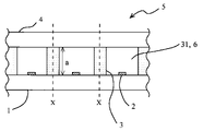
- FIG. 4 is a schematic cross-sectional view showing an example of a process of assembling a cell assembly in a method of manufacturing a unit cell according to an embodiment of the present invention.
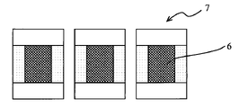
- FIG. 5 is a schematic cross-sectional view showing an example of a unit cell obtained by the unit cell manufacturing method according to the embodiment of the present invention.
- the substrate, the substrate manufacturing method, and the unit cell manufacturing method using the substrate according to the present invention will be described in detail with reference to the illustrated examples as necessary.
- the present invention is not limited to the examples illustrated below, and appropriate modifications can be made within the scope of the gist of the present invention, and all of them are included in the technical scope of the present invention. .
- the substrate 1 of the present invention has a substantially flat surface 11 formed with a plurality of spots 2 of alkali metal azide.
- the substrate is also referred to as "alkali metal azide spotted substrate”.
- the substrate before formation of spots of alkali metal azide is also referred to as a “substrate member”.
- the "substantially flat surface" of the substrate means a surface that does not have large irregularities that may become partition walls for partitioning a plurality of cells when the substrate is used to form a cell assembly. , and may have slight unevenness that does not form the partition wall.
- recesses 12 having a depth of 20% or less of the thickness of the substrate may be formed in spots. Since the alkali metal azide spot-formed substrate 1 does not have portions that serve as partition walls for partitioning a plurality of cells when a cell assembly is formed using the substrate, the size and shape of the unit cells to be produced are limited. High degree of design freedom and high versatility. In addition, since the alkali metal azide spot-forming substrate 1 does not have the partition wall, it can be manufactured without going through a complicated process of individually introducing a raw material as an alkali metal source into each of a plurality of partitioned cells. , can be easily manufactured if necessary.
- the gas cell using the alkali metal azide spot forming substrate 1 is used for an atomic clock, an atomic magnetic sensor, a quantum gyro, etc. utilizing laser spectroscopy, a transparent material having optical transparency is used. Glass having heat resistance is more preferable.
- the thickness of the substrate member 13 can be appropriately set, but from the viewpoint of strength, it is preferably 100 ⁇ m or more, more preferably 500 ⁇ m or more, and from the viewpoint of light transmittance, it is preferably 1.0 mm or less, such as 0.8 mm. The following are more preferred.
- the thickness of the substrate member 13 is the thickness of the portion without the recess 12 .
- the alkali metal azide spot 2 is a spot containing an alkali metal azide, preferably a spot consisting only of an alkali metal azide. If the alkali metal azide spot 2 is a spot consisting only of an alkali metal azide, when a gas cell is produced using the alkali metal azide spot-forming substrate 1, impurities capable of adsorbing buffer gas are present in the cell. It is preferable because it does not occur. If the buffer gas in the cell is adsorbed by impurities, the internal pressure in the cell changes, which may shift the frequency of electromagnetic waves absorbed by the alkali metal or change the temperature characteristics of the alkali metal.
- alkali metal azides examples include lithium azide, sodium azide, potassium azide, rubidium azide, and cesium azide. Rubidium azide and cesium azide are preferred, and rubidium azide is more preferred. Since the transition frequency of rubidium atoms is lower than that of cesium atoms and the like, when a gas cell using the alkali metal azide spot-forming substrate 1 is used for an atomic clock or the like, the alkali metal azide is rubidium azide. Thus, it is possible to keep the power consumption of the electronic circuit low.
- the alkali metal azide is a stable substance at normal temperature and normal pressure, the alkali metal azide spot-forming substrate 1 can be stored and transported at normal temperature and normal pressure.
- the shape of the alkali metal azide spot 2 is not particularly limited, and may be circular, elliptical, or polygonal, for example.
- the size of the spot 2 of the alkali metal azide can be appropriately set, but the equivalent circle diameter of the spot 2 of the alkali metal azide is, for example, preferably 50 ⁇ m or more, more preferably 100 ⁇ m or more, and further preferably 200 ⁇ m or more. Moreover, 2.0 mm or less is preferable and 1.5 mm or less is more preferable.
- the shape and size of the plurality of alkali metal azide spots 2 may be the same or different, but are preferably the same. If the plurality of alkali metal azide spots 2 have the same shape and size, a unit cell with a uniform amount of alkali metal to be enclosed can be easily manufactured using the substrate 1 on which the alkali metal azide spots are formed. . More preferably, the plurality of spots 2 of alkali metal azide are formed as a uniform pattern.
- the alkali metal azide spots 2 may be formed in the depressions 12 .
- the shape of the recess 12 is not particularly limited, and may be, for example, a bowl shape, a bottomed cylinder shape, a bottomed polygonal columnar shape, an inverted cone shape, or an inverted polygonal pyramid shape (bottomed columnar shape in the illustrated example).
- the size of the depression 12 can be set as appropriate, but the outer diameter of the depression 12 is preferably 50 ⁇ m or more, more preferably 100 ⁇ m or more, further preferably 200 ⁇ m or more, further preferably 2.0 mm or less in equivalent circle diameter. , 1.5 mm or less.
- the depth of the depressions 12 is preferably 1 ⁇ m or more, more preferably 10 ⁇ m or more, and more preferably 20 ⁇ m or more, from the viewpoint that the liquid containing the alkali metal azide can be reliably held in the depressions 12 when forming the alkali metal azide spots 2 described later. It is more preferably 200 ⁇ m or less, more preferably 150 ⁇ m or less, and even more preferably 100 ⁇ m or less from the viewpoint of ensuring that the surface 11 is substantially flat.
- the ratio of the depth of the recesses 12 to the thickness of the substrate member 13 is preferably 0.1% or more, more preferably 1% or more, even more preferably 10% or more, preferably 20% or less, and more preferably 18% or less. Preferably, 15% or less is more preferable.
- the shape and size of the plurality of depressions 12 may be the same or different, but are preferably the same. If the shape and size of the plurality of depressions 12 are the same, the shape and size of the plurality of spots 2 of alkali metal azide can be easily made the same, and the unit cell in which the amount of alkali metal enclosed is uniform is the alkali metal azide. It can be easily manufactured using the spot forming substrate 1 .
- a substrate 1 having a plurality of spots 2 of alkali metal azide formed on a substantially flat surface 11 has a coating film formed from a liquid containing alkali metal azide in the form of spots. It can be manufactured by forming on a substrate member 13 having a substantially flat surface 11 on the outside.
- Examples of the alkali metal azide-containing liquid include a solution in which the alkali metal azide is dissolved and a dispersion liquid in which the alkali metal azide is dispersed.
- a solution in which an alkali metal azide is dissolved is preferable because it is easier to make the content more uniform.
- Examples of the solvent for the alkali metal azide-containing liquid include water, methanol, ethanol, isopropyl alcohol, acetonitrile, acetone, N-methylpyrrolidone, dimethylsulfoxide, N,N-dimethylformamide and the like, preferably water or methanol. Methanol is more preferred.
- the concentration of the alkali metal azide in the alkali metal azide-containing liquid is not particularly limited. Weight % or less is more preferred. If the concentration of the alkali metal azide is within the above range, a cell containing an amount of alkali metal suitable for use in atomic devices can be easily obtained.
- an ink jet machine or a dispenser is used to apply an appropriate amount of the alkali metal azide-containing liquid into spots.
- a method of dropping is also included, but the following forming methods A, B and C are preferably included. Formation methods A, B, and C are methods that are possible because the substrate member 13 does not have large unevenness that would serve as partition walls for partitioning a plurality of cells when forming a cell assembly.
- the alkali metal azide spot-formed substrate 1 can be easily manufactured without requiring a complicated step of individually introducing raw materials into each of the partitioned cells.
- a mask surface (mask layer) having spot-like holes is formed on the substantially flat surface 11 of the substrate member 13, and a liquid containing an alkali metal azide is applied to the mask surface.
- a coating film is formed by using a mask, and then the mask is removed.
- the mask having spot-shaped holes in the formation method A is not particularly limited as long as it can be removed in a post-process, and may be an adhesive tape having spot-shaped holes.
- a mask formed of a photomask may be used.
- the coating of the alkali metal azide-containing liquid in the formation method A may be performed using a coating machine such as a spin coater. ) is obtained. If the coating film after drying has a uniform thickness, a unit cell with a uniform amount of alkali metal to be enclosed can be easily manufactured using the alkali metal azide spot-formed substrate 1 .
- the formation of the coating film in the formation method A is performed by removing the liquid component of the liquid containing the alkali metal azide, that is, by drying.
- the drying method is not particularly limited, it may be dried by heating with high-temperature air, a hot plate, or the like.
- a method can be appropriately selected according to the formed mask.
- the adhesive tape may be peeled off so that the adhesive does not remain.
- Formation method B In the forming method B, the substantially flat surface 11 of the substrate member 13 is coated with a solution containing an alkali metal azide to form a coating film, and then the coating film is partially removed to form an alkali metal azide film. In this method, the compound is left in spots on the substantially flat surface 11 .
- the application of the alkali metal azide-containing liquid and the formation of the coating film in the formation method B are the same as the application of the alkali metal azide-containing liquid and the formation of the coating film in the formation method A.
- a photoresist and a photomask which are generally called an etching method, are used. methods and the like.
- the substrate member 13 used in the forming method C has a plurality of depressions 12 formed in advance on at least one side.
- the method for forming the recesses 12 is not particularly limited, and any method that can form a plurality of uniform recesses 12 can be used. Examples thereof include a method of processing with an ultrashort pulse laser and a chemical etching method. Examples and preferred aspects of the shape and size of the recess 12 to be formed are the same as the description of the recess 12 in the description of the substrate 1 above.
- the coating of the alkali metal azide-containing liquid in the formation method C may be performed using a coating machine such as a spin coater so that the alkali metal azide-containing liquid remains only in the depressions 12 of the substrate member 13. .
- a coating machine such as a spin coater
- the liquid other than the recessed portions 12 is left as it is by utilizing the rotational centrifugal force of the spin coater.
- the substrate member 13 after being coated with the alkali metal azide-containing liquid may be tilted or made vertical to remove the liquid other than the recesses 12 . If the substrate member 13 has a plurality of depressions 12, it is not necessary to form a mask surface before forming the coating film or to partially remove the formed coating film.
- the formation of the coating film in the formation method C is the same as the formation of the coating film in the formation method A.
- the manufacturing method of the unit cell 7 shown in FIG. a step of irradiating the cell assembly 5 with ultraviolet rays to vaporize the alkali metal azide, and then a step of cutting out unit cells from the cell assembly 5 .
- the degree of freedom in designing a unit cell is low. Since the shape can be designed appropriately according to the use of the cell, it is possible to manufacture the unit cell 7 with the desired size and shape.
- the cell assembly 5 is a laminate structure in which the alkali metal azide spot-forming substrate 1 and the second substrate 4 are joined together with the partition walls 3 interposed therebetween. By sealing the through hole 31 of the partition wall 3 with the alkali metal azide spot-forming substrate 1 and the second substrate 4, the internal space 6 of the cell is formed as an airtight space.
- the partition wall 3 serves to separate the spots 2 of the alkali metal azide, and is a plate-like member having a plurality of through holes 31 in the thickness direction.
- the material of the partition walls 3 is not particularly limited, and examples thereof include glass, metal, resin, silicon, etc. Glass and silicon, which are suitable for microfabrication such as etching, are preferred, and silicon is more preferred.
- the thickness a (see FIG. 4) of the partition wall 3 can be set as appropriate, but for example, it is preferably 0.1 mm or more, more preferably 0.3 mm or more, preferably 5.0 mm or less, and more preferably 3.0 mm or less.
- the through-holes 31 of the partition walls 3 can be formed by microfabrication such as etching or blasting.
- the size and shape of the through-holes 31 are appropriately set as long as the partition walls 3 do not overlap the alkali metal azide spots 2 of the alkali metal azide spot-forming substrate 1 when the cell assembly 5 is assembled. It is possible. Therefore, the obtained unit cell 7 can have a desired size and shape according to the use of the cell.
- the material of the second substrate 4 since the cell using the substrate is used for an atomic clock, an atomic magnetic sensor, or the like, a transparent member having light transmittance is preferable, and glass having heat resistance is more preferable.
- the thickness of the second substrate 4 can be set as appropriate, for example, it is preferably 80 ⁇ m or more, more preferably 100 ⁇ m or more, and preferably 1.0 mm or less, and more preferably 0.8 mm or less.
- the method of bonding the partition wall 3 to the alkali metal azide spot-formed substrate 1 and the second substrate 4 is not particularly limited and can be appropriately selected according to these materials.
- An activation bonding method or the like can be mentioned, and the anodic bonding method is preferable because it can easily and airtightly bond.
- the bonding between the partition wall 3 and the alkali metal azide spot-forming substrate 1 and the second substrate 4 is preferably performed under vacuum conditions such as in a vacuum chamber.
- the internal state of the alkali metal atoms changes when the single alkali metal in the cell collides with the inner wall of the cell, it is preferable to seal the inside of the cell with a buffer gas.
- Bonding of the azide spot-formed substrate 1 and the second substrate 4 is performed in a buffer gas atmosphere by introducing a buffer gas under vacuum conditions.
- a buffer gas include inert gases such as nitrogen gas, neon gas, argon gas, and a mixed gas of nitrogen gas and argon gas.
- the order of joining the partition walls 3 to the alkali metal azide spot-formed substrate 1 and the second substrate 4 is not particularly limited.
- the barrier ribs 3 and the alkali metal azide spot-forming substrate 1 may be bonded together and then the second substrate 4 may be bonded. 4 may be joined at the same time.
- the partition wall 3 and the alkali metal azide spot-forming substrate 1 alignment between the alkali metal azide spots 2 of the alkali metal azide spot-forming substrate 1 and the through holes 31 of the partition wall 3 is required. to avoid the presence of alkali metal azide on the joint surface.
- the unit cell 7 having a uniform amount of alkali metal enclosed can be manufactured. can do.
- the cell assembly 5 is irradiated with energy rays such as ultraviolet rays to decompose (reduce) the alkali metal azide, thereby vaporizing the alkali metal azide spot-formed substrate 1 , the partition walls 3 , and the second substrate 4 .
- An alkali metal gas is generated in the compartmented internal space 6 of the cell. Nitrogen gas is also generated by the above decomposition, but since nitrogen gas is an inert gas, it can be used as a buffer gas. As described above, if the raw material of the alkali metal is the alkali metal azide, impurities other than the alkali metal gas and the nitrogen gas serving as the buffer gas are not generated. can be reduced.
- Unit cells 7 can be cut out by separating the cell assembly 5 along the dashed line X shown in FIG. 4 by blade dicing, laser dicing, water dicing, or the like.
- the unit cell 7 obtained as described above can be used for atomic devices such as atomic clocks and atomic magnetic sensors.
Landscapes
- Physics & Mathematics (AREA)
- General Physics & Mathematics (AREA)
- Chemical & Material Sciences (AREA)
- Engineering & Computer Science (AREA)
- Life Sciences & Earth Sciences (AREA)
- Thermal Sciences (AREA)
- Plasma & Fusion (AREA)
- Spectroscopy & Molecular Physics (AREA)
- Chemical Kinetics & Catalysis (AREA)
- General Chemical & Material Sciences (AREA)
- Geochemistry & Mineralogy (AREA)
- Materials Engineering (AREA)
- Organic Chemistry (AREA)
- Ecology (AREA)
- Apparatus Associated With Microorganisms And Enzymes (AREA)
Priority Applications (3)
| Application Number | Priority Date | Filing Date | Title |
|---|---|---|---|
| US18/280,747 US12617713B2 (en) | 2021-03-11 | 2022-01-27 | Substrate, method for producing substrate, and method for producing unit cell |
| JP2023505195A JP7730513B2 (ja) | 2021-03-11 | 2022-01-27 | 基板、基板の製造方法、及び単位セルの製造方法 |
| EP22766661.7A EP4307565A4 (en) | 2021-03-11 | 2022-01-27 | Substrate, manufacturing method for substrate and manufacturing method for unit cell |
Applications Claiming Priority (2)
| Application Number | Priority Date | Filing Date | Title |
|---|---|---|---|
| JP2021039388 | 2021-03-11 | ||
| JP2021-039388 | 2021-03-11 |
Publications (1)
| Publication Number | Publication Date |
|---|---|
| WO2022190694A1 true WO2022190694A1 (ja) | 2022-09-15 |
Family
ID=83226650
Family Applications (1)
| Application Number | Title | Priority Date | Filing Date |
|---|---|---|---|
| PCT/JP2022/003180 Ceased WO2022190694A1 (ja) | 2021-03-11 | 2022-01-27 | 基板、基板の製造方法、及び単位セルの製造方法 |
Country Status (3)
| Country | Link |
|---|---|
| EP (1) | EP4307565A4 (https=) |
| JP (1) | JP7730513B2 (https=) |
| WO (1) | WO2022190694A1 (https=) |
Citations (4)
| Publication number | Priority date | Publication date | Assignee | Title |
|---|---|---|---|---|
| JP2012198183A (ja) * | 2011-03-23 | 2012-10-18 | Seiko Epson Corp | ガスセル、ガスセル製造装置およびガスセルの製造方法 |
| JP2014123942A (ja) * | 2012-11-21 | 2014-07-03 | Ricoh Co Ltd | アルカリ金属セルの製造方法及び原子発振器の製造方法 |
| WO2018096730A1 (ja) * | 2016-11-22 | 2018-05-31 | 株式会社村田製作所 | 原子発振器および電子機器 |
| JP2021039388A (ja) | 2017-12-26 | 2021-03-11 | パナソニックIpマネジメント株式会社 | 測位装置及び車両 |
Family Cites Families (6)
| Publication number | Priority date | Publication date | Assignee | Title |
|---|---|---|---|---|
| WO2013072967A1 (ja) * | 2011-11-18 | 2013-05-23 | 株式会社日立製作所 | 磁場計測装置およびその製造方法 |
| JP2016029699A (ja) * | 2014-07-18 | 2016-03-03 | 株式会社リコー | 基板の製造方法、アルカリ金属セルの製造方法、基板複合体、基板複合体の製造方法及びアルカリ金属セル |
| JP2016092465A (ja) * | 2014-10-30 | 2016-05-23 | セイコーエプソン株式会社 | 原子セルの製造方法、原子セル、量子干渉装置、原子発振器、電子機器および移動体 |
| JP2016207695A (ja) * | 2015-04-15 | 2016-12-08 | セイコーエプソン株式会社 | 原子セル、原子セルの製造方法、量子干渉装置、原子発振器、電子機器および移動体 |
| JP2017098373A (ja) * | 2015-11-20 | 2017-06-01 | 株式会社リコー | ガスセル、ガスセルの製造方法、及び原子発振器 |
| US11180844B2 (en) * | 2018-07-02 | 2021-11-23 | Government Of The United States Of America, As Represented By The Secretary Of Commerce | Process for making alkali metal vapor cells |
-
2022
- 2022-01-27 EP EP22766661.7A patent/EP4307565A4/en active Pending
- 2022-01-27 WO PCT/JP2022/003180 patent/WO2022190694A1/ja not_active Ceased
- 2022-01-27 JP JP2023505195A patent/JP7730513B2/ja active Active
Patent Citations (4)
| Publication number | Priority date | Publication date | Assignee | Title |
|---|---|---|---|---|
| JP2012198183A (ja) * | 2011-03-23 | 2012-10-18 | Seiko Epson Corp | ガスセル、ガスセル製造装置およびガスセルの製造方法 |
| JP2014123942A (ja) * | 2012-11-21 | 2014-07-03 | Ricoh Co Ltd | アルカリ金属セルの製造方法及び原子発振器の製造方法 |
| WO2018096730A1 (ja) * | 2016-11-22 | 2018-05-31 | 株式会社村田製作所 | 原子発振器および電子機器 |
| JP2021039388A (ja) | 2017-12-26 | 2021-03-11 | パナソニックIpマネジメント株式会社 | 測位装置及び車両 |
Non-Patent Citations (5)
| Title |
|---|
| H. ZHANGH. HERDIANA. T. NARAYANANA. SHIRANEM. SUZUKIK. HARASAKAK. ADACHIS. GOKAS. YANAGIMACHIK. OKADA: "ULPAC: A Miniatured Ultralow-power Atomic Clock", IEEE JOURNAL OF SOLID-STATE CIRCUITS, vol. 54, no. 11, 2019, pages 3135 - 3148, XP011751671, DOI: 10.1109/JSSC.2019.2941004 |
| J. GOULOUMETB. LEUENBERGERC. SCHORIS. GROPR. ROCHAT: "Progress towards a compact and low-power miniaturized Rubidium Oscillator (mRO", IEEE/MTT-S INTERNATIONAL MICROWAVE SYMPOSIUM, 2020, pages 876 - 879, XP033839644, DOI: 10.1109/IMS30576.2020.9224008 |
| L. LIEWJ. MORELANDV. GERGINOV: "Wafer-level filling of microfabricated atomic vapor cells based on thin-film deposition and photolysis of cesium azide", APPLIED PHYSICS LETTERS, vol. 90, no. 11, 2007, pages 114106, XP012093644, DOI: 10.1063/1.2712501 |
| S. KARLENJ. GOBETT. OVERSTOLZJ. HAESLERS. LECOMTE: "Lifetime assessment of RbN -filled MEMS atomic vapor cells with AI O coating", OPTICS EXPRESS, vol. 25, no. 3, 2017, pages 2187 - 2194 |
| See also references of EP4307565A4 |
Also Published As
| Publication number | Publication date |
|---|---|
| JP7730513B2 (ja) | 2025-08-28 |
| EP4307565A1 (en) | 2024-01-17 |
| EP4307565A4 (en) | 2025-03-19 |
| JPWO2022190694A1 (https=) | 2022-09-15 |
| US20240150229A1 (en) | 2024-05-09 |
Similar Documents
| Publication | Publication Date | Title |
|---|---|---|
| CN104188626B (zh) | 气室的制造方法及气室、磁测定装置的制造方法及磁测定装置 | |
| US8906470B2 (en) | Method for producing a microfabricated atomic vapor cell | |
| US10527422B2 (en) | Micro three-dimensional shell resonator gyroscope | |
| US8637137B2 (en) | Microstructures and methods of fabrication thereof | |
| Straessle et al. | Microfabricated alkali vapor cell with anti-relaxation wall coating | |
| Queste et al. | Manufacture of microfluidic glass chips by deep plasma etching, femtosecond laser ablation, and anodic bonding | |
| JP5994408B2 (ja) | パッケージの封止方法およびガスセルの製造方法 | |
| CN107850870A (zh) | 适用于原子传感器的气室以及填充气室的方法 | |
| JP2016207695A (ja) | 原子セル、原子セルの製造方法、量子干渉装置、原子発振器、電子機器および移動体 | |
| US7666485B2 (en) | Alkali metal-wax micropackets for alkali metal handling | |
| JP2012509201A (ja) | 微小表面構造の形成方法および微小電気機械部材の製造方法、微小表面構造、ならびに当該構造を有する微小電気機械部材 | |
| WO2022190694A1 (ja) | 基板、基板の製造方法、及び単位セルの製造方法 | |
| JP7821810B2 (ja) | 基準ガスをmemsセル内に封入する方法 | |
| JP6217261B2 (ja) | 原子セルの製造方法 | |
| US12617713B2 (en) | Substrate, method for producing substrate, and method for producing unit cell | |
| JP6036230B2 (ja) | アルカリ金属セルの製造方法及び原子発振器の製造方法 | |
| CN115744811A (zh) | 异形排布的多气份原子气室封装方法、产品及使用方法 | |
| JP2015046535A (ja) | アルカリ金属セルの製造方法及び原子発振器の製造方法 | |
| JP6447678B2 (ja) | 原子セルの製造方法、原子セル、量子干渉装置、原子発振器および電子機器 | |
| Hirai et al. | Low temperature, wafer-level process of alkali-metal vapor cells for micro-fabricated atomic clocks | |
| Kiyose et al. | Microfabricated alkali metal vapor cells filled with an on-chip dispensing component | |
| CN116081567A (zh) | 一种具有内壁保护层的微型原子气室及制备方法 | |
| Liew et al. | Micromachined alkali atom vapor cells for chip-scale atomic clocks | |
| Gorecki | Development of first European chip-scale atomic clocks: Technologies, assembling and metrology | |
| JP6519627B2 (ja) | ガスセル |
Legal Events
| Date | Code | Title | Description |
|---|---|---|---|
| 121 | Ep: the epo has been informed by wipo that ep was designated in this application |
Ref document number: 22766661 Country of ref document: EP Kind code of ref document: A1 |
|
| WWE | Wipo information: entry into national phase |
Ref document number: 2023505195 Country of ref document: JP |
|
| WWE | Wipo information: entry into national phase |
Ref document number: 18280747 Country of ref document: US |
|
| WWE | Wipo information: entry into national phase |
Ref document number: 2022766661 Country of ref document: EP |
|
| NENP | Non-entry into the national phase |
Ref country code: DE |
|
| ENP | Entry into the national phase |
Ref document number: 2022766661 Country of ref document: EP Effective date: 20231011 |