WO2022190456A1 - 電界効果トランジスタとその製造方法 - Google Patents
電界効果トランジスタとその製造方法 Download PDFInfo
- Publication number
- WO2022190456A1 WO2022190456A1 PCT/JP2021/040836 JP2021040836W WO2022190456A1 WO 2022190456 A1 WO2022190456 A1 WO 2022190456A1 JP 2021040836 W JP2021040836 W JP 2021040836W WO 2022190456 A1 WO2022190456 A1 WO 2022190456A1
- Authority
- WO
- WIPO (PCT)
- Prior art keywords
- type
- layer
- trench
- lower layer
- type deep
- Prior art date
- Legal status (The legal status is an assumption and is not a legal conclusion. Google has not performed a legal analysis and makes no representation as to the accuracy of the status listed.)
- Ceased
Links
Images


Classifications
-
- H—ELECTRICITY
- H10—SEMICONDUCTOR DEVICES; ELECTRIC SOLID-STATE DEVICES NOT OTHERWISE PROVIDED FOR
- H10D—INORGANIC ELECTRIC SEMICONDUCTOR DEVICES
- H10D62/00—Semiconductor bodies, or regions thereof, of devices having potential barriers
- H10D62/10—Shapes, relative sizes or dispositions of the regions of the semiconductor bodies; Shapes of the semiconductor bodies
- H10D62/124—Shapes, relative sizes or dispositions of the regions of semiconductor bodies or of junctions between the regions
- H10D62/126—Top-view geometrical layouts of the regions or the junctions
- H10D62/127—Top-view geometrical layouts of the regions or the junctions of cellular field-effect devices, e.g. multicellular DMOS transistors or IGBTs
-
- H—ELECTRICITY
- H10—SEMICONDUCTOR DEVICES; ELECTRIC SOLID-STATE DEVICES NOT OTHERWISE PROVIDED FOR
- H10D—INORGANIC ELECTRIC SEMICONDUCTOR DEVICES
- H10D62/00—Semiconductor bodies, or regions thereof, of devices having potential barriers
- H10D62/10—Shapes, relative sizes or dispositions of the regions of the semiconductor bodies; Shapes of the semiconductor bodies
- H10D62/102—Constructional design considerations for preventing surface leakage or controlling electric field concentration
- H10D62/103—Constructional design considerations for preventing surface leakage or controlling electric field concentration for increasing or controlling the breakdown voltage of reverse-biased devices
- H10D62/105—Constructional design considerations for preventing surface leakage or controlling electric field concentration for increasing or controlling the breakdown voltage of reverse-biased devices by having particular doping profiles, shapes or arrangements of PN junctions; by having supplementary regions, e.g. junction termination extension [JTE]
-
- H—ELECTRICITY
- H10—SEMICONDUCTOR DEVICES; ELECTRIC SOLID-STATE DEVICES NOT OTHERWISE PROVIDED FOR
- H10D—INORGANIC ELECTRIC SEMICONDUCTOR DEVICES
- H10D30/00—Field-effect transistors [FET]
- H10D30/01—Manufacture or treatment
- H10D30/021—Manufacture or treatment of FETs having insulated gates [IGFET]
- H10D30/028—Manufacture or treatment of FETs having insulated gates [IGFET] of double-diffused metal oxide semiconductor [DMOS] FETs
- H10D30/0291—Manufacture or treatment of FETs having insulated gates [IGFET] of double-diffused metal oxide semiconductor [DMOS] FETs of vertical DMOS [VDMOS] FETs
- H10D30/0297—Manufacture or treatment of FETs having insulated gates [IGFET] of double-diffused metal oxide semiconductor [DMOS] FETs of vertical DMOS [VDMOS] FETs using recessing of the gate electrodes, e.g. to form trench gate electrodes
-
- H—ELECTRICITY
- H10—SEMICONDUCTOR DEVICES; ELECTRIC SOLID-STATE DEVICES NOT OTHERWISE PROVIDED FOR
- H10D—INORGANIC ELECTRIC SEMICONDUCTOR DEVICES
- H10D30/00—Field-effect transistors [FET]
- H10D30/60—Insulated-gate field-effect transistors [IGFET]
- H10D30/64—Double-diffused metal-oxide semiconductor [DMOS] FETs
- H10D30/66—Vertical DMOS [VDMOS] FETs
- H10D30/668—Vertical DMOS [VDMOS] FETs having trench gate electrodes, e.g. UMOS transistors
-
- H—ELECTRICITY
- H10—SEMICONDUCTOR DEVICES; ELECTRIC SOLID-STATE DEVICES NOT OTHERWISE PROVIDED FOR
- H10D—INORGANIC ELECTRIC SEMICONDUCTOR DEVICES
- H10D62/00—Semiconductor bodies, or regions thereof, of devices having potential barriers
- H10D62/01—Manufacture or treatment
- H10D62/051—Forming charge compensation regions, e.g. superjunctions
- H10D62/058—Forming charge compensation regions, e.g. superjunctions by using trenches, e.g. implanting into sidewalls of trenches or refilling trenches
-
- H—ELECTRICITY
- H10—SEMICONDUCTOR DEVICES; ELECTRIC SOLID-STATE DEVICES NOT OTHERWISE PROVIDED FOR
- H10D—INORGANIC ELECTRIC SEMICONDUCTOR DEVICES
- H10D62/00—Semiconductor bodies, or regions thereof, of devices having potential barriers
- H10D62/10—Shapes, relative sizes or dispositions of the regions of the semiconductor bodies; Shapes of the semiconductor bodies
- H10D62/102—Constructional design considerations for preventing surface leakage or controlling electric field concentration
- H10D62/103—Constructional design considerations for preventing surface leakage or controlling electric field concentration for increasing or controlling the breakdown voltage of reverse-biased devices
- H10D62/105—Constructional design considerations for preventing surface leakage or controlling electric field concentration for increasing or controlling the breakdown voltage of reverse-biased devices by having particular doping profiles, shapes or arrangements of PN junctions; by having supplementary regions, e.g. junction termination extension [JTE]
- H10D62/106—Constructional design considerations for preventing surface leakage or controlling electric field concentration for increasing or controlling the breakdown voltage of reverse-biased devices by having particular doping profiles, shapes or arrangements of PN junctions; by having supplementary regions, e.g. junction termination extension [JTE] having supplementary regions doped oppositely to or in rectifying contact with regions of the semiconductor bodies, e.g. guard rings with PN or Schottky junctions
- H10D62/107—Buried supplementary regions, e.g. buried guard rings
-
- H—ELECTRICITY
- H10—SEMICONDUCTOR DEVICES; ELECTRIC SOLID-STATE DEVICES NOT OTHERWISE PROVIDED FOR
- H10D—INORGANIC ELECTRIC SEMICONDUCTOR DEVICES
- H10D62/00—Semiconductor bodies, or regions thereof, of devices having potential barriers
- H10D62/10—Shapes, relative sizes or dispositions of the regions of the semiconductor bodies; Shapes of the semiconductor bodies
- H10D62/102—Constructional design considerations for preventing surface leakage or controlling electric field concentration
- H10D62/103—Constructional design considerations for preventing surface leakage or controlling electric field concentration for increasing or controlling the breakdown voltage of reverse-biased devices
- H10D62/105—Constructional design considerations for preventing surface leakage or controlling electric field concentration for increasing or controlling the breakdown voltage of reverse-biased devices by having particular doping profiles, shapes or arrangements of PN junctions; by having supplementary regions, e.g. junction termination extension [JTE]
- H10D62/109—Reduced surface field [RESURF] PN junction structures
- H10D62/111—Multiple RESURF structures, e.g. double RESURF or 3D-RESURF structures
-
- H—ELECTRICITY
- H10—SEMICONDUCTOR DEVICES; ELECTRIC SOLID-STATE DEVICES NOT OTHERWISE PROVIDED FOR
- H10D—INORGANIC ELECTRIC SEMICONDUCTOR DEVICES
- H10D62/00—Semiconductor bodies, or regions thereof, of devices having potential barriers
- H10D62/10—Shapes, relative sizes or dispositions of the regions of the semiconductor bodies; Shapes of the semiconductor bodies
- H10D62/13—Semiconductor regions connected to electrodes carrying current to be rectified, amplified or switched, e.g. source or drain regions
- H10D62/149—Source or drain regions of field-effect devices
- H10D62/151—Source or drain regions of field-effect devices of IGFETs
- H10D62/156—Drain regions of DMOS transistors
- H10D62/157—Impurity concentrations or distributions
Definitions
- the technology disclosed in this specification relates to a field effect transistor and its manufacturing method.
- Japanese Patent Application Laid-Open No. 2009-194065 discloses a trench gate type field effect transistor.
- This field effect transistor has a plurality of p-type deep layers protruding downward from the body layer. Each p-type deep layer extends to intersect the trench when the semiconductor substrate is viewed from above. The plurality of p-type deep layers are arranged with intervals in the width direction. Each p-type deep layer extends from the body layer to below the bottom surface of the trench.
- each p-type deep layer is in contact with the gate insulating film on the side surface and the bottom surface of the trench located below the body layer.
- the field effect transistor also has an n-type drift layer in contact with the body layer and each p-type deep layer.
- a depletion layer spreads from the body layer into the drift layer.
- a depletion layer extending into the drift layer holds the source-drain voltage.
- a depletion layer spreads from each deep p-layer into the drift layer as well. Since each deep p-layer is in contact with the gate insulating film at the bottom of the trench, the drift layer around the bottom of the trench is depleted by the depletion layer spreading from each deep p-layer.
- the depletion layer extending from each deep p layer to the periphery of the bottom surface of the trench suppresses the occurrence of electric field concentration in the gate insulating film and the drift layer around the bottom surface of the trench. Therefore, this field effect transistor has a high withstand voltage.
- a field effect transistor having such a plurality of p-type deep layers requires a technique for further alleviating the electric field concentration in the gate insulating film around the bottom of the trench and increasing the withstand voltage.
- This specification proposes a technique for realizing a high withstand voltage in a field effect transistor having a plurality of p-type deep layers.
- a field effect transistor disclosed in the present specification includes a semiconductor substrate having a trench on its upper surface, a gate insulating film covering the inner surface of the trench, and a gate insulating film disposed in the trench.
- a gate electrode that is insulated from the The semiconductor substrate comprises an n-type source layer in contact with the gate insulating film on side surfaces of the trench, and a p-type body layer in contact with the gate insulating film on the side surfaces of the trench located below the source layer.
- a p-type trench lower layer disposed below the trench and extending along the longitudinal direction of the trench when the semiconductor substrate is viewed from above; a plurality of p-type deep layers; Can have a mold deep layer.
- Each of the p-type deep layers protrudes downward from the body layer, extends from the body layer to below the bottom surface of the trench, and extends relative to the trench when the semiconductor substrate is viewed from above. extending along a first direction intersecting with each other, are spaced apart in a second direction orthogonal to the first direction when the semiconductor substrate is viewed from above, and are located below the trench. the p-type trench lower layer located on the side. Each of the n-type deep layers is arranged in the corresponding space and is in contact with the gate insulating film on the side surface of the trench located below the body layer.
- This field effect transistor has a p-type trench underlayer arranged on the underside of the trench. Therefore, the electric field concentration around the bottom of the trench is relaxed when the field effect transistor is turned off. As a result, this field effect transistor can have a high withstand voltage. Furthermore, in this field effect transistor, the p-type trench lower layer is electrically connected to the body layer through a plurality of p-type deep layers. Therefore, the potential of the lower layer of the p-type trench is stabilized, and deterioration of the switching characteristics of the field effect transistor is suppressed. As described above, in this field effect transistor, the combination of the p-type trench lower layer and the plurality of p-type deep layers can improve the withstand voltage while suppressing the deterioration of the switching characteristics.
- a method for manufacturing a field effect transistor disclosed in the present specification includes a deep layer forming step of forming a plurality of p-type deep layers and a plurality of n-type deep layers in an n-type epitaxial layer, wherein each p-type deep layer extend along a first direction when the epitaxial layer is viewed from above, and are spaced apart in a second direction orthogonal to the first direction when the epitaxial layer is viewed from above a deep layer forming step in which each of the n-type deep layers is arranged in the corresponding space; and from the surface of the epitaxial layer, the plurality of p-type deep layers and the plurality of n-type deep layers.
- a trench forming step for forming a trench having a depth not exceeding a layer, wherein the trench intersects the plurality of p-type deep layers and the plurality of n-type deep layers when the epitaxial layer is viewed from above.
- a trench forming step and an ion implantation technique are used to introduce a p-type impurity toward the surface of the epitaxial layer, and a body is formed above the plurality of p-type deep layers and the plurality of n-type deep layers.
- a field effect transistor having a p-type trench lower layer and a plurality of p-type deep layers can be manufactured.
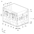
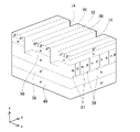
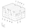
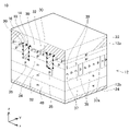
- FIG. 2 is a cross-sectional perspective view of the MOSFET 10 (a diagram showing an xz cross section that does not include the p-type deep layer 36).
- FIG. 2 is a cross-sectional perspective view of the MOSFET 10 omitting the source electrode 22 and the interlayer insulating film 20 (a diagram showing the xz cross section that does not include the p-type deep layer 36).
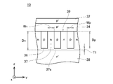
- FIG. 2 is an enlarged cross-sectional view of MOSFET 10 showing the arrangement of deep layer 37;
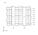
- 2 is an enlarged xy cross section including trench 14, p-type deep layer 36 and n-type deep layer 37, showing the arrangement of trench 14, p-type deep layer 36 and n-type deep layer 37 when semiconductor substrate 12 is viewed from above;
- FIG. 2 is an enlarged cross-sectional view of MOSFET 10 shown;
- FIG. 2 is an enlarged yz cross-sectional view of MOSFET 10 including p-type deep layer 36 and n-type deep layer 37;
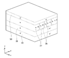
- FIG. 2 is a cross-sectional perspective view of the MOSFET 10 (a diagram showing the xz cross section including the p-type deep layer 36).
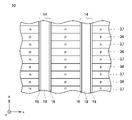
- FIG. 2 is an enlarged xy cross section including the trench 14, the p-type deep layer 36 and the n-type deep layer 37, showing the arrangement of the trench 14, the p-type deep layer 36 and the n-type deep layer 37 when the semiconductor substrate 12 is viewed from above;
- FIG. 4 is an enlarged cross-sectional view of a modification of the MOSFET 10 shown;
- 2 is an enlarged xy cross section including the trench 14, the p-type deep layer 36 and the n-type deep layer 37, showing the arrangement of the trench 14, the p-type deep layer 36 and the n-type deep layer 37 when the semiconductor substrate 12 is viewed from above;
- FIG. 4 is an enlarged cross-sectional view of a modification of the MOSFET 10 shown;
- 2 is an enlarged xy cross section including the trench 14, the p-type deep layer 36 and the n-type deep layer 37, showing the arrangement of the trench 14, the p-type deep layer 36 and the n-type deep layer 37 when the semiconductor substrate 12 is
- FIG. 4 is an enlarged cross-sectional view of a modification of the MOSFET 10 shown; An enlarged xy cross section including the p-type trench lower layer 35, the p-type deep layer 36 and the n-type deep layer 37 as viewed from above the semiconductor substrate 12, the p-type trench lower layer 35, the p-type deep layer 36 and the n-type FIG. 4 is an enlarged cross-sectional view of a modification of MOSFET 10 showing the arrangement of deep layer 37; FIG. 4 is a cross-sectional perspective view of a modified example of the MOSFET 10 omitting the source electrode 22 and the interlayer insulating film 20 (a diagram showing the xz cross section that does not include the p-type deep layer 36).
- FIG. 4 is a cross-sectional perspective view of a modified example of the MOSFET 10 omitting the source electrode 22 and the interlayer insulating film 20 (a diagram showing the xz cross section that does not include the p-type deep layer 36).
- FIG. 4 is a cross-sectional perspective view of a modification of the MOSFET 10 (a diagram showing an xz cross section that does not include the p-type deep layer 36).
- FIG. 4 is a cross-sectional perspective view of a modification of the MOSFET 10 (a diagram showing an xz cross section including the p-type deep layer 36).
- FIG. 4 is a cross-sectional perspective view of a modification of the MOSFET 10 (a diagram showing an xz cross section that does not include the p-type deep layer 36).
- FIG. 4 is a cross-sectional perspective view of a modification of the MOSFET 10 (a diagram showing an xz cross section including the p-type deep layer 36). Explanatory drawing of the manufacturing method of MOSFET10.
- FIG. 4 is a cross-sectional perspective view of a modification of the MOSFET 10 (a diagram showing an xz cross section that does not include the p-type deep layer 36).
- the MOSFET 10 metal-oxide-semiconductor field effect transistor
- the thickness direction of the semiconductor substrate 12 is referred to as the z-direction
- one direction parallel to the upper surface 12a of the semiconductor substrate 12 is referred to as the x-direction
- the direction perpendicular to the x-direction and the z-direction. is called the y-direction.
- the semiconductor substrate 12 is made of silicon carbide (that is, SiC).
- the semiconductor substrate 12 may be made of other semiconductor materials such as silicon and gallium nitride.
- a plurality of trenches 14 are provided in the upper surface 12 a of the semiconductor substrate 12 . As shown in FIG. 2, the plurality of trenches 14 elongate along the y direction on the upper surface 12a. The multiple trenches 14 are spaced apart in the x-direction.
- each trench 14 is covered with a gate insulating film 16 .
- a gate electrode 18 is disposed within each trench 14 .
- Each gate electrode 18 is insulated from the semiconductor substrate 12 by a gate insulating film 16 .
- the top surface of each gate electrode 18 is covered with an interlayer insulating film 20 .
- a source electrode 22 is provided on the semiconductor substrate 12 .
- a source electrode 22 covers each interlayer insulating film 20 .
- the source electrode 22 is insulated from the gate electrode 18 by the interlayer insulating film 20 .
- the source electrode 22 is in contact with the upper surface 12a of the semiconductor substrate 12 at a position where the interlayer insulating film 20 does not exist.
- a drain electrode 24 is arranged below the semiconductor substrate 12 .
- the drain electrode 24 is in contact with the entire lower surface 12 b of the semiconductor substrate 12 .
- the semiconductor substrate 12 includes a plurality of source layers 30, a plurality of contact layers 32, a body layer 34, a plurality of p-type trench lower layers 35, a plurality of p-type deep layers 36, and a plurality of n-type layers 36. It has a deep layer 37 , a drift layer 38 and a drain layer 40 .
- Each source layer 30 is an n-type layer having a high n-type impurity concentration. Each source layer 30 is arranged in a range partially including the upper surface 12 a of the semiconductor substrate 12 . Each source layer 30 is in ohmic contact with the source electrode 22 . Each source layer 30 is in contact with the gate insulating film 16 at the uppermost side of the trench 14 . Each source layer 30 faces the gate electrode 18 with the gate insulating film 16 interposed therebetween. Each source layer 30 extends long in the y-direction along the side surface of the trench 14 . That is, each source layer 30 extends parallel to the longitudinal direction of the trench 14 when the semiconductor substrate 12 is viewed from above, and extends from one longitudinal end of the trench 14 to the other longitudinal end. ing.
- Each contact layer 32 is a p-type layer having a high p-type impurity concentration. Each contact layer 32 is arranged in a range partially including the upper surface 12 a of the semiconductor substrate 12 . Each contact layer 32 is arranged between two corresponding source layers 30 . Each contact layer 32 is in ohmic contact with the source electrode 22 . Each contact layer 32 extends long in the y direction. That is, each contact layer 32 extends parallel to the longitudinal direction of the trench 14 when the semiconductor substrate 12 is viewed from above, and extends from one longitudinal end of the trench 14 to the other longitudinal end. ing.
- the body layer 34 is a p-type layer having a p-type impurity concentration lower than that of the contact layer 32 .
- the body layer 34 is arranged below the plurality of source layers 30 and the plurality of contact layers 32 .
- the body layer 34 is in contact with the plurality of source layers 30 and the plurality of contact layers 32 from below.
- the body layer 34 is in contact with the gate insulating film 16 on the side surface of the trench 14 located below the source layer 30 .
- the body layer 34 faces the gate electrode 18 with the gate insulating film 16 interposed therebetween.
- Each p-type trench lower layer 35 is a p-type layer arranged below the corresponding trench 14 .
- each p-type trench lower layer 35 may be formed in the same ion implantation process as that of the body layer 34 .
- the p-type impurity concentration profiles in the depth direction of each p-type trench lower layer 35 and body layer 34 match, and the depth from the bottom surface of the corresponding trench 14 to the bottom surface of each p-type trench lower layer 35 is , corresponds to the depth from the upper surface 12 a of the semiconductor substrate 12 to the lower surface of the body layer 34 .
- each p-type trench lower layer 35 is in contact with the gate insulating film 16 covering the bottom surface of the corresponding trench 14 .
- each p-type trench lower layer 35 extends long along the longitudinal direction of the corresponding trench 14 (the y direction in this example). may extend continuously from one longitudinal end to the other longitudinal end. As will be described later, each p-type trench lower layer 35 extends along the longitudinal direction of the corresponding trench 14 (the y-direction in this example), and is divided between one end and the other end of the trench 14 in the longitudinal direction. You may have
- Each p-type deep layer 36 is a p-type layer projecting downward from the lower surface of the body layer 34 .
- the p-type impurity concentration of each p-type deep layer 36 is higher than the p-type impurity concentration of the body layer 34 and lower than the p-type impurity concentration of the contact layer 32 .
- each p-type deep layer 36 extends long in the x direction and is perpendicular to the longitudinal direction of the trench 14 (in this example, the y direction). is doing.
- a plurality of p-type deep layers 36 are arranged at intervals in the y direction.
- a portion between the plurality of p-type deep layers 36 is hereinafter referred to as an interval portion 39 (see FIGS. 1 and 2).
- the p-type deep layer 36 has a shape elongated in the z direction in the yz cross section. That is, the dimension of the p-type deep layer 36 in the z direction (hereinafter referred to as depth Dp) is larger than the dimension of the p-type deep layer 36 in the y direction (hereinafter referred to as width Wp).
- the depth Dp can be 1-4 times the width Wp.
- each p-type deep layer 36 extends from the bottom surface of the body layer 34 to a depth below the bottom surface of each trench 14 .
- Each p-type deep layer 36 is in contact with the gate insulating film 16 on the side surface of the trench 14 located below the body layer 34 .
- each p-type deep layer 36 is in contact with the p-type trench lower layer 35 arranged below the trench 14 so as to intersect.
- Each n-type deep layer 37 is an n-type layer having a higher n-type impurity concentration than the drift layer 38 .
- the n-type impurity concentration of each n-type deep layer 37 is lower than the p-type impurity concentration of each p-type deep layer 36 .
- each n-type deep layer 37 may have the same concentration as the n-type impurity concentration of the drift layer 38 .
- each n-type deep layer 37 is arranged within a corresponding spacing portion 39 .
- Each n-type deep layer 37 is in contact with the bottom surface of the body layer 34 .
- Each n-type deep layer 37 is in contact with the side surfaces of the p-type deep layers 36 on both sides thereof.
- Each n-type deep layer 37 extends from the bottom surface of the body layer 34 to below the bottom surface of each trench 14 and the bottom surface of each p-type deep layer 36 .
- the n-type deep layer 37 in the spacing portion 39 has a shape elongated in the z direction in the yz cross section. That is, the dimension of the n-type deep layer 37 in the z-direction (hereinafter referred to as depth Dn) is larger than the dimension in the y-direction of the n-type deep layer 37 in the spacing portion 39 (hereinafter referred to as width Wn).
- the depth Dn can be 1-4 times the width Wn.
- the width Wn of the n-type deep layer 37 is approximately equal to the width Wp of the p-type deep layer 36 .
- Each n-type deep layer 37 has a connection region 37a extending directly below the lower surface of the adjacent p-type deep layer 36 .
- Each connection region 37 a is in contact with the lower surface of the corresponding p-type deep layer 36 .
- Each n-type deep layer 37 is connected to each other through each connection region 37a.
- the thickness T1 of the portion where the n-type deep layer 37 protrudes below the bottom surface of the p-type deep layer 36 is It is about 0.1 ⁇ m and extremely thin.
- each n-type deep layer 37 is in contact with the gate insulating film 16 on the side surface of the trench 14 located below the body layer 34 within each spacing portion 39 .
- each n-type deep layer 37 is in contact with the p-type trench lower layer 35 arranged below the trench 14 so as to intersect.
- the drift layer 38 is an n-type layer having a lower n-type impurity concentration than each n-type deep layer 37 .
- the drift layer 38 is arranged below the n-type deep layer 37 .
- the drift layer 38 is in contact with the n-type deep layer 37 from below.
- the drain layer 40 is an n-type layer having a higher n-type impurity concentration than the drift layer 38 and the n-type deep layer 37 .
- the drain layer 40 is in contact with the drift layer 38 from below.
- the drain layer 40 is arranged in a range including the lower surface 12b of the semiconductor substrate 12 .
- the drain layer 40 is in ohmic contact with the drain electrode 24 .
- the MOSFET 10 is used with the drain electrode 24 applied with a higher potential than the source electrode 22 .
- a potential equal to or higher than the gate threshold is applied to each gate electrode 18, a channel is formed in the body layer 34 near the gate insulating film 16.
- FIG. The channel connects the source layer 30 and the n-type deep layer 37 . Therefore, electrons flow from the source layer 30 to the drain layer 40 via the channel, the n-type deep layer 37 and the drift layer 38 . That is, the MOSFET 10 is turned on.
- the potential of each gate electrode 18 is lowered from a value above the gate threshold to a value below the gate threshold, the channel disappears and electron flow stops. That is, the MOSFET 10 is turned off.
- each p-type deep layer 36 is electrically connected to the body layer 34 and has substantially the same potential as the body layer 34 . Therefore, when the channel disappears, a reverse voltage is also applied to the pn junction at the interface between each p-type deep layer 36 and each n-type deep layer 37 . Therefore, a depletion layer spreads from each p-type deep layer 36 to each n-type deep layer 37 as well.
- each p-type trench lower layer 35 is electrically connected to the body layer 34 via each p-type deep layer 36 and has substantially the same potential as the body layer 34 . Therefore, when the channel disappears, a reverse voltage is also applied to the pn junction at the interface between each p-type trench lower layer 35 and each n-type deep layer 37 . Thus, each n-type deep layer 37 is quickly depleted by the depletion layer spreading from the body layer 34 , each p-type trench lower layer 35 and each p-type deep layer 36 . In particular, since each p-type trench lower layer 35 is provided under the corresponding trench 14, the periphery of the bottom surface of the trench 14 is well depleted.
- each n-type deep layer 37 is entirely depleted by a depletion layer extending from the body layer 34 , each p-type trench lower layer 35 and each p-type deep layer 36 . Since each n-type deep layer 37 has a higher n-type impurity concentration than the drift layer 38 , a depletion layer is less likely to spread in each n-type deep layer 37 than in the drift layer 38 . However, since each n-type deep layer 37 is sandwiched between p-type deep layers 36 and the width Wn of each n-type deep layer 37 is narrow, each n-type deep layer 37 is entirely depleted.
- MOSFET 10 has a high withstand voltage.
- the p-type trench lower layer 35 is electrically connected to the body layer 34 via the p-type deep layer 36 . Therefore, the potential of the p-type trench lower layer 35 is stabilized, and deterioration of the switching characteristics of the MOSFET 10 can be suppressed.
- the combination of the p-type trench lower layer 35 and the p-type deep layer 36 can improve the breakdown voltage while suppressing the deterioration of the switching characteristics.
- each n-type deep layer 37 and each p-type deep layer 36 have a vertically long shape. When each n-type deep layer 37 and each p-type deep layer 36 are configured in this manner, the feedback capacitance is reduced. These can improve the switching speed of the MOSFET 10 .
- the p-type trench lower layer 35 is deeper than the p-type deep layer 36 and the n-type deep layer 37 .
- the provision of such a deep p-type trench lower layer 35 promotes depletion of the n-type deep layer 37 and the drift layer 38 , thereby improving the withstand voltage of the MOSFET 10 .
- breakdown occurs in the p-type trench lower layer 35 protruding downward when an overvoltage is applied, so that breakdown occurs reliably in the cell region. can be made As a result, the avalanche resistance of the MOSFET 10 can also be stabilized.
- the depth of the p-type trench lower layer 35 may be shallower than the depths of the p-type deep layer 36 and the n-type deep layer 37 . In this case, since the depletion layer extending from the p-type trench lower layer 35 is suppressed, the on-resistance of the MOSFET 10 is improved.
- each p-type deep layer 36 and each n-type deep layer 37 are continuous in the x direction between adjacent trenches 14. It was growing long. Instead of this example, as shown in FIG. 7, each p-type deep layer 36 and each n-type deep layer 37 may be separated in the x direction. In this example, since each p-type deep layer 36 is divided, a wide current path is ensured and the on-resistance is lowered. However, even in this example, each p-type deep layer 36 and each n-type deep layer 37 are arranged so as to straddle the trench 14 . Thereby, the above-described effects can be exhibited.
- each p-type deep layer 36 and each n-type deep layer 37 may be divided in the x direction. Further, as shown in FIG. 8, a connection p layer 36a may be provided to connect the p-type deep layers 36 adjacent to each other in the y direction. Such a connection p-layer 36a is effective in alleviating the electric field applied to the gate insulating film 16 and improving the withstand voltage.
- each p-type trench lower layer 35 extends continuously from one longitudinal end to the other longitudinal end of the trench 14 when the semiconductor substrate 12 is viewed from above.
- each p-type trench lower layer 35 when the semiconductor substrate 12 is viewed from above, each p-type trench lower layer 35 extends along the longitudinal direction of the corresponding trench 14 (the y direction in this example). It extends and may be divided between one longitudinal end of the trench 14 and the other longitudinal end. In this case, each p-type deep layer 36 passes through the divided portion of the p-type trench lower layer 35 .
- FIG. 9 when the semiconductor substrate 12 is viewed from above, each p-type trench lower layer 35 extends along the longitudinal direction of the corresponding trench 14 (the y direction in this example). It extends and may be divided between one longitudinal end of the trench 14 and the other longitudinal end.
- each p-type deep layer 36 passes through the divided portion of the p-type trench lower layer 35 .
- the portion where the p-type trench lower layer 35 and the p-type deep layer 36 overlap is greatly damaged during ion implantation, and there is concern about an increase in leakage current.
- the overlapping portion between the p-type trench lower layer 35 and the p-type deep layer 36 is small, an increase in leakage current can be suppressed.
- each source layer 30 and each contact layer 32 extends parallel to the longitudinal direction of the trench 14 when the semiconductor substrate 12 is viewed from above, as shown in FIG.
- the entire side surface of the trench 14 can be used as a high-concentration channel. Low ON resistance.
- the entire side surface of the trench 14 can be used as a channel, the channel and each n-type deep layer 37 are well connected.
- each source layer 30 extends crosswise to the longitudinal direction of the trench 14 , particularly perpendicular to the longitudinal direction of the trench 14 , the position of the source layer 30 adjacent to the side surface of the trench 14 is is limited, the position of the high-concentration channel formed on the side surface of the trench 14 is also limited. Therefore, in such an example, due to a relative positional deviation between the source layer 30 and the n-type deep layer 37 during manufacturing, the high-concentration channel formed on the side surface of the trench 14 and the n-type deep layer 37 are separated from each other. Since the relative positional relationship is also shifted, there is a problem that the on-resistance tends to fluctuate greatly.
- the contact layers 32 may be distributed along the longitudinal direction of the trench 14 as shown in FIG. Also in this example, it can be said that each contact layer 32 extends parallel to the longitudinal direction of the trench 14 when the semiconductor substrate 12 is viewed from above. Also, in this example, the source layer 30 may be provided between the contact layers 32 .
- the n-type deep layer 37 may have an n-type deep lower layer 137A and an n-type deep upper layer 137B.
- the n-type deep lower layer 137A is provided below the n-type deep upper layer 137B, and is an n-type layer having a higher n-type impurity concentration than the drift layer 38 and a lower n-type impurity concentration than the n-type deep upper layer 137B.
- the n-type impurity concentration of the n-type deep lower layer 137A may be the same concentration as when configured with substantially a single concentration as described above.
- the n-type deep upper layer 137B is provided between the n-type deep lower layer 137A and the body layer 34, is arranged above the bottom surface of the trench 14, and is located on the side surface of the trench 14 located below the body layer 34. is in contact with the gate insulating film 16 at .
- the depletion layer extending from both the p-type trench lower layer 35 and the body layer 34 narrows the current path in the region between the p-type trench lower layer 35 and the body layer 34.
- a phenomenon JFET effect
- the n-type deep layer 37 has the n-type deep lower layer 137A and the n-type deep upper layer 137B, and the n-type deep upper layer 137B is arranged above the bottom surface of the trench 14, thereby suppressing an increase in on-resistance. High withstand voltage can be satisfactorily compatible.
- the p-type deep layer 36 may have a p-type deep lower layer 136A and a p-type deep upper layer 136B.
- the p-type deep lower layer 136A is provided below the p-type deep upper layer 136B, and is a p-type layer having a higher p-type impurity concentration than the body layer 34 and a lower p-type impurity concentration than the p-type deep upper layer 136B.
- the p-type deep upper layer 136B is provided between the p-type deep lower layer 136A and the body layer 34, is arranged above the bottom surface of the trench 14, and is located on the side surface of the trench 14 located below the body layer 34.
- the concentration of the entire p-type deep layer 36 is high. increases, and there is concern about an increase in leakage current.
- the breakdown voltage can be improved while suppressing an increase in leakage current.
- the p-type trench lower layer 35 may have a first p-type trench lower layer 135A and a second p-type trench lower layer 135B.
- the first p-type trench lower layer 135A is provided below the second p-type trench lower layer 135B, and is a p-type layer with a lower p-type impurity concentration than the second p-type trench lower layer 135B.
- the second p-type trench lower layer 135B is provided between the first p-type trench lower layer 135A and the trench 14, and is in contact with the gate insulating film 16 at the bottom surface of the trench 14. As shown in FIG.
- the thickness of the second p-type trench lower layer 135B in the depth direction (z direction) may be smaller than the thickness of the source layer 30 in the thickness direction.
- the product of the p-type impurity concentration and thickness of the second p-type trench lower layer 135B may be greater than the product of the n-type impurity concentration and thickness of the n-type deep layer 37 . If the second p-type trench lower layer 135B having a high p-type impurity concentration is provided, the second p-type trench lower layer 135B will not be depleted when the MOSFET 10 is turned off. As a result, the capacitance (that is, the feedback capacitance) between the gate electrode 18 and the drain electrode 24 is reduced, and the switching speed of the MOSFET 10 can be improved.
- the relationship of p-type impurity concentration between the first p-type trench lower layer 135A and the second p-type trench lower layer 135B in FIG. 13 may be reversed. That is, the p-type impurity concentration of the second p-type trench lower layer 135B may be lower than the p-type impurity concentration of the first p-type trench lower layer 135A. Also in this case, the thickness of the second p-type trench lower layer 135B in the depth direction (z direction) may be smaller than the thickness of the source layer 30 in the thickness direction.
- the p-type trench lower layer 35 may be separated from the bottom surface of the trench 14, as shown in FIG.
- the distance between the p-type trench lower layer 35 and the bottom surface of the trench 14 may be smaller than the thickness of the source layer 30 in the thickness direction. Even if the p-type trench lower layer 35 is provided in such a positional relationship, the effect of improving the breakdown voltage described above can be obtained.
- such a p-type trench lower layer 35 has a form that reflects the result of reducing the number of times of ion implantation for the body layer 34 that is simultaneously formed. That is, the MOSFET 10 shown in FIG. 14 has a structure that can be manufactured at low cost.
- the depth of the n-type deep layer 37 was deeper than the depth of the p-type deep layer 36 .
- the depth of the n-type deep layer 37 may be equal to the depth of the p-type deep layer 36 .
- the depth of the n-type deep layer 37 may be shallower than the depth of the p-type deep layer 36 .
- each n-type deep layer 37 has a connection region 37a extending directly below the p-type deep layer 36 .
- the n-type deep layer 37 may not have the connection region 37a.
- each p-type deep layer 36 and each n-type deep layer 37 were orthogonal to each trench 14 when the semiconductor substrate 12 was viewed from above. Instead of this example, each p-type deep layer 36 and each n-type deep layer 37 may obliquely cross each trench 14 .
- MOSFET 10 is fabricated from a semiconductor substrate entirely constituted by drain layer 40 .
- an epitaxial growth technique is used to form an n-type epitaxial layer 50 on the drain layer 40 .
- an ion implantation technique is used to introduce n-type impurities and p-type impurities into a predetermined depth range apart from the surface of the epitaxial layer 50, thereby n-type deep layer 37 and p-type impurity.
- a mold deep layer 36 is formed (an example of a deep layer forming step). Specifically, after doping the n-type impurity from the surface toward a predetermined depth of the epitaxial layer 50, the p-type impurity is counter-doped through a mask toward a part of the range where the n-type impurity has been introduced. Thus, the n-type deep layer 37 and the p-type deep layer 36 can be formed.
- n-type deep layer 37 and p-type deep layer 37 and p-type deep layer 37 are formed by sequentially introducing n-type impurities and p-type impurities through masks respectively corresponding to n-type deep layer 37 and p-type deep layer 36 .
- a layer 36 may be formed.
- ion implantation for forming the n-type deep layer 37 is omitted by previously adjusting the concentration of the n-type impurity to a depth corresponding to the formation range of the n-type deep layer 37 when the epitaxial layer 50 is epitaxially grown. be able to.
- the n-type deep layer 37 or the p-type deep layer 36 is formed using the ion implantation technique or the epitaxial growth technique, by changing the concentration in the depth direction, the n-type deep lower layer as shown in FIG. 137A and n-type deep upper layer 137B or p-type deep lower layer 136A and p-type deep upper layer 136B as shown in FIG. 12 can be formed.
- the source layer 30 and the contact layer 32 are formed by introducing an n-type impurity and a p-type impurity into the surface layer portion of the epitaxial layer 50 using an ion implantation technique.
- an etching technique is used to form trenches 14 extending from the surface of the epitaxial layer 50 to the n-type deep layer 37 and the p-type deep layer 36 (an example of the trench forming process).
- the depth of trench 14 is adjusted so as not to exceed n-type deep layer 37 and p-type deep layer 36 .
- the trench 14 crosses a plurality of p-type deep layers 36 and a plurality of n-type deep layers 37 when the epitaxial layer 50 is viewed from above.
- the body layer 34 and the p-type trench lower layer 35 are formed by introducing p-type impurities in multiple stages toward the surface of the epitaxial layer 50 using an ion implantation technique (body layer 34 and p-type trench lower layer 35).
- body layer 34 and p-type trench lower layer 35 An example of a layer forming process and a p-type trench lower layer forming process).
- the body layer 34 is formed above the n-type deep layer 37 and the p-type deep layer 36 and below the source layer 30 and the contact layer 32 .
- a p-type trench lower layer 35 is formed below the bottom surface of the trench 14 .
- the first p-type trench lower layer 135A and the first p-type trench lower layer 135A and the first p-type trench lower layer 135A as shown in FIG. A 2p-type trench underlayer 135B may be formed.
- the depth to which the p-type impurity is introduced to form the second p-type trench lower layer 135B is limited to a range shallower than the source layer 30 . Thereby, the p-type impurity concentration of the second p-type trench lower layer 135B can be freely set while the p-type impurity concentration of the body layer 34 is set to a desired value.
- the concentration of the n-type impurity contained in the source layer 30 is higher than the concentration of the introduced p-type impurity. Therefore, the electrical characteristics of the MOSFET 10 are not greatly changed.
- ion implantation is performed so that the p-type impurity is selectively introduced into a range above the n-type deep layer 37 and the p-type deep layer 36 and below the source layer 30 and the contact layer 32 .
- the p-type trench lower layer 35 is formed at a position away from the bottom surface of the trench 14 .
- MOSFET 10 shown in FIG. 14 is an example manufactured by such a method.
- a soak prevention shielding film may be formed on the side surface of the trench 14 before ion-implanting the p-type impurity.
- the trench 14, the gate insulating film 16, the gate electrode 18, the interlayer insulating film 20, the source electrode 22, and the drain electrode 24 are formed to complete the MOSFET 10.
- various semiconductor regions can be formed using an ion implantation technique without performing a re-epi process.
- the MOSFET 10 with a low feedback capacitance can be manufactured without performing the re-epi process.
- the MOSFET 10 of the present embodiment may be manufactured by carrying out a re-epi process, if necessary.
- the MOSFET 10 described above is an example in which the body layer 34 and the p-type trench lower layer 35 are simultaneously formed using an ion implantation technique after forming the trench 14 .
- the p-type trench lower layer 35 and the p-type deep layer 36 may be formed simultaneously before forming the trench 14 .
- the body layer 34 is formed by another ion implantation process.
- FIG. 20 shows a MOSFET 10 in which a p-type trench lower layer 35 and a p-type deep layer 36 are formed simultaneously.
- the width of the p-type trench lower layer 35 is narrower than the width of the trench 14 when measured along the lateral direction (x direction) of the trench 14 .
- a slight misalignment between the p-type trench lower layer 35 and the trench 14 can be allowed, so that when the trench 14 is formed, the p-type trench lower layer 35 is arranged so as to contact only the bottom surface of the trench 14 . can do.
- a field-effect transistor disclosed in the present specification includes a semiconductor substrate having a trench on its upper surface, a gate insulating film covering the inner surface of the trench, and a gate insulating film disposed in the trench.
- the material of the semiconductor substrate is not particularly limited, but may be silicon carbide, for example.
- the semiconductor substrate comprises an n-type source layer in contact with the gate insulating film on side surfaces of the trench, and a p-type body layer in contact with the gate insulating film on the side surfaces of the trench located below the source layer.
- a p-type trench lower layer disposed below the trench and extending along the longitudinal direction of the trench when the semiconductor substrate is viewed from above; a plurality of p-type deep layers; Can have a mold deep layer.
- Each of the p-type deep layers protrudes downward from the body layer, extends from the body layer to below the bottom surface of the trench, and extends relative to the trench when the semiconductor substrate is viewed from above.
- extending along a first direction intersecting with each other are spaced apart in a second direction orthogonal to the first direction when the semiconductor substrate is viewed from above, and are located below the trench.
- the p-type trench lower layer located on the side.
- Each of the n-type deep layers is arranged in the corresponding space and is in contact with the gate insulating film on the side surface of the trench located below the body layer.
- the source layer may extend parallel to the longitudinal direction of the trench when the semiconductor substrate is viewed from above. In this field effect transistor, fluctuations in on-resistance are suppressed.
- the semiconductor substrate may have a contact layer provided on the body layer and having a p-type impurity concentration higher than that of the body layer.
- the contact layer may extend parallel to the longitudinal direction of the trench when the semiconductor substrate is viewed from above.
- the p-type trench lower layer may protrude below the p-type deep layers.
- This field effect transistor can have a high withstand voltage.
- the p-type trench lower layer may be shallower than each of the p-type deep layers. This field effect transistor can have a low on-resistance.
- the semiconductor substrate may further include a drift layer arranged below each of the n-type deep layers and having an n-type impurity concentration lower than that of each of the n-type deep layers. good.
- each n-type deep layer may have a higher n-type impurity concentration than the drift layer.
- This field effect transistor can have a low on-resistance.
- each of the n-type deep layers is arranged above the n-type deep lower layer and the n-type deep lower layer, and has an n-type impurity concentration higher than that of the n-type deep lower layer.
- an upper layer In this case, the n-type deep upper layer is arranged above the bottom surface of the trench.
- each of the p-type deep layers is arranged above the p-type deep lower layer and the p-type deep lower layer, and has a p-type impurity concentration higher than that of the p-type deep lower layer.
- an upper layer In this case, the p-type deep upper layer is arranged above the bottom surface of the trench.
- This field effect transistor can have a high withstand voltage while suppressing an increase in leakage current.
- the depth from the bottom surface of the corresponding trench to the bottom surface of each p-type trench lower layer may match the depth from the top surface of the semiconductor substrate to the bottom surface of the body layer.
- This field effect transistor has a form reflecting the result of simultaneous formation of the p-type trench lower layer and the body layer.
- This field effect transistor has a structure that can be manufactured at low cost.
- the p-type trench lower layer may be separated from the bottom surface of the trench.
- This field effect transistor has a form reflecting the result of reducing the number of times of ion implantation of the body layer formed at the same time.
- This field effect transistor has a structure that can be manufactured at low cost.
- the p-type trench lower layer may have a plurality of portions with different concentrations in the depth direction.
- the p-type trench lower layer may have a first p-type trench lower layer and a second p-type trench lower layer disposed above the first p-type trench lower layer.
- the second p-type trench lower layer may have a higher concentration than the first p-type trench lower layer, and may have a lower concentration than the first p-type trench lower layer.
- the thickness of the second p-type trench lower layer in the depth direction may be smaller than the thickness of the source layer in the depth direction.
- the feedback capacitance can be adjusted by adjusting the impurity concentration of the p-type trench lower layer.
- the p-type trench lower layer may be divided along the longitudinal direction of the trench.
- Each of the p-type deep layers may pass through a divided portion of the p-type trench lower layer. This field effect transistor suppresses an increase in leakage current.
- the plurality of n-type deep layers may extend from the bottom surface of the body layer to below the bottom surfaces of the plurality of p-type deep layers.
- the first direction may be orthogonal to the trench when the semiconductor substrate is viewed from above.
- a method for manufacturing a field effect transistor disclosed in the present specification includes a deep layer forming step of forming a plurality of p-type deep layers and a plurality of n-type deep layers in an n-type epitaxial layer, wherein each p-type deep layer extend along a first direction when the epitaxial layer is viewed from above, and are spaced apart in a second direction orthogonal to the first direction when the epitaxial layer is viewed from above a deep layer forming step in which each of the n-type deep layers is arranged in the corresponding space; and from the surface of the epitaxial layer, the plurality of p-type deep layers and the plurality of n-type deep layers.
- a trench forming step and an ion implantation technique are used to introduce a p-type impurity toward the surface of the epitaxial layer, and a body is formed above the plurality of p-type deep layers and the plurality of n-type deep layers.
- an ion implantation technique is used to form the plurality of p-type deep layers and the plurality of n-type deep layers in a predetermined depth range apart from the surface of the epitaxial layer with n-type impurities and p-type layers. It may be formed by introducing type impurities. According to this manufacturing method, a field effect transistor can be manufactured without performing a re-epi process.
- the body layer forming step and the p-type trench lower layer forming step may be performed simultaneously after the trench forming step. According to this manufacturing method, a field effect transistor can be manufactured at low cost.
- the manufacturing method may further include a source layer forming step of introducing an n-type impurity into the upper layer portion of the epitaxial layer to form a source layer using an ion implantation technique.
- the p-type trench lower layer may have a first p-type trench lower layer and a second p-type trench lower layer arranged above the first p-type trench lower layer.
- the second p-type trench lower layer may have a higher concentration than the first p-type trench lower layer, and may have a lower concentration than the first p-type trench lower layer.
- the thickness of the second p-type trench lower layer in the depth direction may be smaller than the thickness of the source layer in the depth direction.
- the p-type trench lower layer forming step may be performed before the trench forming step.
- the width of the p-type trench lower layer may be narrower than the width of the trench. According to this manufacturing method, a slight misalignment between the p-type trench lower layer and the trench can be allowed.
- the p-type trench lower layer forming step may be performed simultaneously with the step of forming the plurality of p-type deep layers in the deep layer forming step. According to this manufacturing method, a field effect transistor can be manufactured at low cost.
Landscapes
- Metal-Oxide And Bipolar Metal-Oxide Semiconductor Integrated Circuits (AREA)
- Insulated Gate Type Field-Effect Transistor (AREA)
- Electrodes Of Semiconductors (AREA)
Priority Applications (4)
| Application Number | Priority Date | Filing Date | Title |
|---|---|---|---|
| CN202180094906.2A CN116918072A (zh) | 2021-03-11 | 2021-11-05 | 场效应晶体管及其制造方法 |
| EP21930302.1A EP4307382A4 (en) | 2021-03-11 | 2021-11-05 | Field-effect transistor, and method for manufacturing same |
| EP25154724.6A EP4525583A3 (en) | 2021-03-11 | 2021-11-05 | Field-effect transistor, and method for manufacturing same |
| US18/446,919 US20230387194A1 (en) | 2021-03-11 | 2023-08-09 | Field effect transistor and method of manufacturing the same |
Applications Claiming Priority (6)
| Application Number | Priority Date | Filing Date | Title |
|---|---|---|---|
| JP2021039221 | 2021-03-11 | ||
| JP2021-039221 | 2021-03-11 | ||
| JP2021069123 | 2021-04-15 | ||
| JP2021-069123 | 2021-04-15 | ||
| JP2021-103917 | 2021-06-23 | ||
| JP2021103917A JP7537377B2 (ja) | 2021-03-11 | 2021-06-23 | 電界効果トランジスタとその製造方法 |
Related Child Applications (1)
| Application Number | Title | Priority Date | Filing Date |
|---|---|---|---|
| US18/446,919 Continuation US20230387194A1 (en) | 2021-03-11 | 2023-08-09 | Field effect transistor and method of manufacturing the same |
Publications (1)
| Publication Number | Publication Date |
|---|---|
| WO2022190456A1 true WO2022190456A1 (ja) | 2022-09-15 |
Family
ID=83227816
Family Applications (1)
| Application Number | Title | Priority Date | Filing Date |
|---|---|---|---|
| PCT/JP2021/040836 Ceased WO2022190456A1 (ja) | 2021-03-11 | 2021-11-05 | 電界効果トランジスタとその製造方法 |
Country Status (5)
| Country | Link |
|---|---|
| US (1) | US20230387194A1 (enExample) |
| EP (2) | EP4525583A3 (enExample) |
| JP (3) | JP7537377B2 (enExample) |
| CN (1) | CN116918072A (enExample) |
| WO (1) | WO2022190456A1 (enExample) |
Cited By (1)
| Publication number | Priority date | Publication date | Assignee | Title |
|---|---|---|---|---|
| WO2025084070A1 (ja) * | 2023-10-16 | 2025-04-24 | ローム株式会社 | 半導体装置 |
Families Citing this family (8)
| Publication number | Priority date | Publication date | Assignee | Title |
|---|---|---|---|---|
| JP2022191131A (ja) * | 2021-06-15 | 2022-12-27 | 富士電機株式会社 | 半導体装置 |
| JP7717010B2 (ja) * | 2022-03-08 | 2025-08-01 | 株式会社デンソー | 半導体装置 |
| CN115911093A (zh) * | 2022-11-11 | 2023-04-04 | 天狼芯半导体(成都)有限公司 | 碳化硅mosfet的结构、制造方法及电子设备 |
| WO2024176583A1 (ja) * | 2023-02-24 | 2024-08-29 | 株式会社デンソー | 電界効果トランジスタの製造方法 |
| KR20250093007A (ko) * | 2023-12-15 | 2025-06-24 | 주식회사 엘엑스세미콘 | 전력반도체 소자 및 이를 포함하는 전력변환 장치 |
| WO2025183975A1 (en) * | 2024-03-01 | 2025-09-04 | Semiconductor Components Industries, Llc | Electronic device including a power transistor including a buried shield and a gap region and a process of making the same |
| WO2025192705A1 (ja) * | 2024-03-14 | 2025-09-18 | 株式会社デンソー | 半導体装置およびその製造方法 |
| KR20250139672A (ko) * | 2024-03-15 | 2025-09-23 | 현대모비스 주식회사 | 전력 반도체 장치 |
Citations (8)
| Publication number | Priority date | Publication date | Assignee | Title |
|---|---|---|---|---|
| JP2009194065A (ja) | 2008-02-13 | 2009-08-27 | Denso Corp | 炭化珪素半導体装置およびその製造方法 |
| JP2010225615A (ja) * | 2009-03-19 | 2010-10-07 | Denso Corp | 炭化珪素半導体装置およびその製造方法 |
| JP2012169384A (ja) * | 2011-02-11 | 2012-09-06 | Denso Corp | 炭化珪素半導体装置およびその製造方法 |
| JP2012169386A (ja) * | 2011-02-11 | 2012-09-06 | Denso Corp | 炭化珪素半導体装置およびその製造方法 |
| JP2015046628A (ja) * | 2014-11-06 | 2015-03-12 | 三菱電機株式会社 | 炭化珪素半導体装置 |
| WO2016157606A1 (ja) * | 2015-03-30 | 2016-10-06 | 三菱電機株式会社 | 炭化珪素半導体装置およびその製造方法 |
| JP2018113421A (ja) * | 2017-01-13 | 2018-07-19 | トヨタ自動車株式会社 | 半導体装置の製造方法 |
| JP2020109809A (ja) * | 2019-01-07 | 2020-07-16 | 株式会社デンソー | 半導体装置 |
Family Cites Families (10)
| Publication number | Priority date | Publication date | Assignee | Title |
|---|---|---|---|---|
| JP4640436B2 (ja) * | 2008-04-14 | 2011-03-02 | 株式会社デンソー | 炭化珪素半導体装置の製造方法 |
| JP5747447B2 (ja) * | 2010-06-01 | 2015-07-15 | 日立化成株式会社 | ドナー元素拡散機能を有する電極形成用ペースト組成物、太陽電池セル、及び太陽電池セルの製造方法 |
| JP5136674B2 (ja) * | 2010-07-12 | 2013-02-06 | 株式会社デンソー | 半導体装置およびその製造方法 |
| JP6111673B2 (ja) * | 2012-07-25 | 2017-04-12 | 住友電気工業株式会社 | 炭化珪素半導体装置 |
| JP2016025177A (ja) * | 2014-07-18 | 2016-02-08 | トヨタ自動車株式会社 | スイッチング素子 |
| WO2017098547A1 (ja) * | 2015-12-07 | 2017-06-15 | 三菱電機株式会社 | 炭化珪素半導体装置 |
| JP6880669B2 (ja) * | 2016-11-16 | 2021-06-02 | 富士電機株式会社 | 炭化珪素半導体装置および炭化珪素半導体装置の製造方法 |
| JP2019102556A (ja) * | 2017-11-29 | 2019-06-24 | 富士電機株式会社 | 半導体装置および半導体装置の製造方法 |
| JP7056390B2 (ja) * | 2018-06-07 | 2022-04-19 | 株式会社豊田中央研究所 | 窒化物半導体装置の製造方法 |
| JP7263178B2 (ja) * | 2019-08-02 | 2023-04-24 | 株式会社東芝 | 半導体装置、インバータ回路、駆動装置、車両、及び、昇降機 |
-
2021
- 2021-06-23 JP JP2021103917A patent/JP7537377B2/ja active Active
- 2021-11-05 EP EP25154724.6A patent/EP4525583A3/en active Pending
- 2021-11-05 WO PCT/JP2021/040836 patent/WO2022190456A1/ja not_active Ceased
- 2021-11-05 CN CN202180094906.2A patent/CN116918072A/zh active Pending
- 2021-11-05 EP EP21930302.1A patent/EP4307382A4/en active Pending
-
2023
- 2023-08-09 US US18/446,919 patent/US20230387194A1/en active Pending
-
2024
- 2024-07-29 JP JP2024121992A patent/JP7750347B2/ja active Active
-
2025
- 2025-09-09 JP JP2025149204A patent/JP2025168586A/ja active Pending
Patent Citations (8)
| Publication number | Priority date | Publication date | Assignee | Title |
|---|---|---|---|---|
| JP2009194065A (ja) | 2008-02-13 | 2009-08-27 | Denso Corp | 炭化珪素半導体装置およびその製造方法 |
| JP2010225615A (ja) * | 2009-03-19 | 2010-10-07 | Denso Corp | 炭化珪素半導体装置およびその製造方法 |
| JP2012169384A (ja) * | 2011-02-11 | 2012-09-06 | Denso Corp | 炭化珪素半導体装置およびその製造方法 |
| JP2012169386A (ja) * | 2011-02-11 | 2012-09-06 | Denso Corp | 炭化珪素半導体装置およびその製造方法 |
| JP2015046628A (ja) * | 2014-11-06 | 2015-03-12 | 三菱電機株式会社 | 炭化珪素半導体装置 |
| WO2016157606A1 (ja) * | 2015-03-30 | 2016-10-06 | 三菱電機株式会社 | 炭化珪素半導体装置およびその製造方法 |
| JP2018113421A (ja) * | 2017-01-13 | 2018-07-19 | トヨタ自動車株式会社 | 半導体装置の製造方法 |
| JP2020109809A (ja) * | 2019-01-07 | 2020-07-16 | 株式会社デンソー | 半導体装置 |
Non-Patent Citations (1)
| Title |
|---|
| See also references of EP4307382A4 |
Cited By (1)
| Publication number | Priority date | Publication date | Assignee | Title |
|---|---|---|---|---|
| WO2025084070A1 (ja) * | 2023-10-16 | 2025-04-24 | ローム株式会社 | 半導体装置 |
Also Published As
| Publication number | Publication date |
|---|---|
| EP4307382A1 (en) | 2024-01-17 |
| EP4307382A4 (en) | 2024-10-23 |
| JP2022140217A (ja) | 2022-09-26 |
| US20230387194A1 (en) | 2023-11-30 |
| CN116918072A (zh) | 2023-10-20 |
| JP2024138119A (ja) | 2024-10-07 |
| JP2025168586A (ja) | 2025-11-07 |
| JP7750347B2 (ja) | 2025-10-07 |
| EP4525583A3 (en) | 2025-06-25 |
| JP7537377B2 (ja) | 2024-08-21 |
| EP4525583A2 (en) | 2025-03-19 |
Similar Documents
| Publication | Publication Date | Title |
|---|---|---|
| JP7537377B2 (ja) | 電界効果トランジスタとその製造方法 | |
| US10546950B2 (en) | Semiconductor device | |
| US10276666B2 (en) | Semiconductor device | |
| JP7326725B2 (ja) | 半導体装置 | |
| TWI565059B (zh) | Semiconductor device | |
| US20110049615A1 (en) | Power semiconductor device | |
| JP6593294B2 (ja) | 半導体装置 | |
| JP7616033B2 (ja) | 半導体装置の製造方法 | |
| WO2022190444A1 (ja) | 電界効果トランジスタ | |
| JP2025159185A (ja) | 電界効果トランジスタ | |
| JP2025122207A (ja) | 半導体装置とその製造方法 | |
| JP2024137200A (ja) | 電界効果トランジスタ | |
| US20250380468A1 (en) | Method for producing field effect transistor | |
| JP7628874B2 (ja) | 半導体装置及びその製造方法 | |
| WO2025192705A1 (ja) | 半導体装置およびその製造方法 | |
| JP2024131786A (ja) | 半導体装置 | |
| US20230163174A1 (en) | Shielding Structure for Silicon Carbide Devices | |
| KR20190071333A (ko) | 반도체 소자 및 그 제조 방법 | |
| WO2024203285A1 (ja) | 窒化物半導体装置 | |
| WO2025187565A1 (ja) | 半導体装置およびその製造方法 | |
| JP2025138452A (ja) | 半導体装置 | |
| JP2025107910A (ja) | 電界効果トランジスタ | |
| JP2024071835A (ja) | 半導体装置 | |
| JP2020096083A (ja) | トレンチゲート型のスイッチング素子の製造方法 | |
| KR20190071332A (ko) | 반도체 소자 및 그 제조 방법 |
Legal Events
| Date | Code | Title | Description |
|---|---|---|---|
| 121 | Ep: the epo has been informed by wipo that ep was designated in this application |
Ref document number: 21930302 Country of ref document: EP Kind code of ref document: A1 |
|
| WWE | Wipo information: entry into national phase |
Ref document number: 202180094906.2 Country of ref document: CN |
|
| WWE | Wipo information: entry into national phase |
Ref document number: 2021930302 Country of ref document: EP |
|
| NENP | Non-entry into the national phase |
Ref country code: DE |
|
| ENP | Entry into the national phase |
Ref document number: 2021930302 Country of ref document: EP Effective date: 20231011 |