WO2022168898A1 - 昇圧装置 - Google Patents
昇圧装置 Download PDFInfo
- Publication number
- WO2022168898A1 WO2022168898A1 PCT/JP2022/004155 JP2022004155W WO2022168898A1 WO 2022168898 A1 WO2022168898 A1 WO 2022168898A1 JP 2022004155 W JP2022004155 W JP 2022004155W WO 2022168898 A1 WO2022168898 A1 WO 2022168898A1
- Authority
- WO
- WIPO (PCT)
- Prior art keywords
- overcurrent
- control unit
- booster
- boosting
- monitoring circuit
- Prior art date
- Legal status (The legal status is an assumption and is not a legal conclusion. Google has not performed a legal analysis and makes no representation as to the accuracy of the status listed.)
- Ceased
Links
Images


Classifications
-
- H—ELECTRICITY
- H02—GENERATION; CONVERSION OR DISTRIBUTION OF ELECTRIC POWER
- H02M—APPARATUS FOR CONVERSION BETWEEN AC AND AC, BETWEEN AC AND DC, OR BETWEEN DC AND DC, AND FOR USE WITH MAINS OR SIMILAR POWER SUPPLY SYSTEMS; CONVERSION OF DC OR AC INPUT POWER INTO SURGE OUTPUT POWER; CONTROL OR REGULATION THEREOF
- H02M3/00—Conversion of DC power input into DC power output
- H02M3/02—Conversion of DC power input into DC power output without intermediate conversion into AC
- H02M3/04—Conversion of DC power input into DC power output without intermediate conversion into AC by static converters
- H02M3/10—Conversion of DC power input into DC power output without intermediate conversion into AC by static converters using discharge tubes with control electrode or semiconductor devices with control electrode
- H02M3/145—Conversion of DC power input into DC power output without intermediate conversion into AC by static converters using discharge tubes with control electrode or semiconductor devices with control electrode using devices of a triode or transistor type requiring continuous application of a control signal
- H02M3/155—Conversion of DC power input into DC power output without intermediate conversion into AC by static converters using discharge tubes with control electrode or semiconductor devices with control electrode using devices of a triode or transistor type requiring continuous application of a control signal using semiconductor devices only
Definitions
- the present disclosure relates to a booster.
- An object of the present disclosure is to provide a booster that simplifies the circuit configuration and shortens the start-up time in a booster that prevents erroneous determination of an overcurrent abnormality.
- the present disclosure is a boosting device that boosts and outputs an input power supply voltage.
- This booster includes a boost switching element, a drive circuit, an overcurrent monitoring circuit, and a controller.
- the boost switching element is provided between the ground and the other end of the coil, one end of which is connected to the power supply, and boosts the voltage of the other end of the coil by switching operation.
- the drive circuit PWM-operates the boost switching element.
- the overcurrent monitoring circuit monitors the current flowing through the boost switching element.
- the control unit determines an abnormality based on the notification from the overcurrent monitoring circuit and takes measures.
- the overcurrent monitoring circuit transmits a notification signal to the control unit when the first condition is satisfied regarding the state of the current flowing through the boost switching element.
- the control unit determines that there is an abnormality and takes action.
- the overcurrent monitoring circuit does not make an abnormality determination merely by detecting an overcurrent, and transmits a notification signal to the control unit when the first condition is satisfied. Further, the control unit judges abnormality for the first time when the second condition is established, and takes measures. Therefore, it is possible to avoid erroneously determining that an overcurrent is abnormal when the power is turned on or when the initial check is performed.
- a soft start circuit is not used, and an overcurrent is detected with respect to an overcurrent threshold value set below the rating of the boost switching element at the time of power-on or initial check. power on while In other words, erroneous determination is prevented by preventing the second condition from being satisfied while assuming that the first condition is likely to be satisfied at the time of power-on or initial check. This simplifies the circuit configuration and shortens the start-up time.
- FIG. 1 is a configuration diagram of the booster and its surroundings according to the first embodiment
- FIG. 2 is a schematic configuration diagram of an electric power steering device to which the boost device according to the first embodiment is applied
- FIG. 3 is a circuit diagram showing an overcurrent that occurs when a short circuit fault occurs in a diode or coil
- FIG. 4 is a time chart showing the operation of the boosting device according to the first embodiment
- FIG. 5 is a time chart explaining an example in which the first condition is satisfied
- FIG. 6 is a configuration diagram of an overcurrent detection threshold value setting unit
- FIG. 7 is a flowchart showing the processing when overcurrent is detected
- FIG. 8 is a flowchart of abnormality determination
- FIG. 9 is a flow chart showing a process for preventing erroneous determination
- FIG. 10 is a flow chart showing a procedure when an abnormality is determined
- FIG. 11 is a configuration diagram of the booster and its surroundings according to the second embodiment.
- a booster device boosts a power supply voltage in an electric power steering device for a vehicle.
- the reference numerals of the boosting devices of the first and second embodiments are denoted as "301" and "302", respectively, and the common matters are described as the description of the boosting device 301.
- FIG. 1st Embodiment and 2nd Embodiment differ in the element which functions as a "control part.”
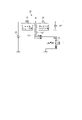
- FIG. 1 shows the configuration of a booster device 301 and its surroundings according to the first embodiment.
- the booster circuit 20 boosts and outputs the power supply voltage input from the battery 15 so that the operation can be continued even when the voltage of the battery 15 is low.
- a voltage before being boosted by the boosting circuit 20 is denoted as VL, and a voltage after being boosted is denoted as VH.
- the inverter 60 also converts the DC power of the battery 15 into AC power and supplies the AC power to the motor 80 .
- Motor 80 is, for example, a three-phase brushless motor.
- the booster circuit 20 is a chopper-type booster circuit including a coil 21, a diode 23, a capacitor 24, and a booster MOS 25 as a "boost switching element".
- the boost MOS 25 is composed of an n-channel MOSFET. In this specification, MOSFET is omitted and simply referred to as "MOS".
- One end of the coil 21 is connected to the battery 15 as a "power supply”. Elements such as a power relay 16 and a diode (not shown) may be connected between the battery 15 and the coil 21 .
- the power relay 16 may be a mechanical relay or a semiconductor switching element.
- the diode 23 has an anode connected to the other end of the coil 21 and a cathode connected to the output terminal.
- a capacitor 24 is provided between the cathode of the diode 23 and the ground.
- the boost MOS 25 is provided between the connection point N at the other end of the coil 21 and the ground. That is, the drain terminal is connected to the connection point N, and the source terminal is grounded. A gate terminal of the boosting MOS 25 is connected to the drive circuit 41 .
- the boost MOS 25 performs switching operation based on the PWM command signal output from the drive circuit 41 .
- the coil 21 repeats accumulation and release of inductive energy, so that the voltage at the other end of the coil 21, that is, the output side is boosted.
- the boosting MOS 25 boosts the voltage on the output side of the coil 21 by switching operation.
- the boosting device 301 of the first embodiment includes at least the boosting MOS 25 among the components of the boosting circuit 20 .
- the booster 301 also includes a drive circuit 41, an overcurrent monitoring circuit 44, and a microcomputer 50 as a "control section".
- the drive circuit 41 causes the boost MOS 25 to perform PWM operation.
- the overcurrent monitoring circuit 44 monitors the current flowing through the boost MOS 25 and detects overcurrent. The technical significance of the overcurrent monitoring circuit 44 will be described later.
- the boost MOS 25, drive circuit 41 and overcurrent monitoring circuit 44 are built in the same IC.
- This IC is referred to herein as an ASIC 40, which stands for Application Specific IC.
- the overcurrent monitoring circuit 44 detects overcurrent, the overcurrent monitoring circuit 44 commands the drive circuit 41 to forcibly turn off the boost MOS 25 as a protection function.
- the ASIC 40 and the microcomputer 50 that constitute the booster 301 communicate with each other.
- the microcomputer 50 determines an abnormality based on the notification from the overcurrent monitoring circuit and takes measures. Specifically, the overcurrent monitoring circuit 44 outputs a notification signal indicating overcurrent detection to the microcomputer 50 .
- the microcomputer 50 instructs the drive circuit 41 to stop the operation of the boost MOS 25, for example, as a measure to be taken when the abnormality is determined.
- the microcomputer 50 monitors a monitoring voltage, which is "a voltage monitored by a circuit before or after boosting". For example, as the voltage of the circuit before boosting, the power supply voltage of the battery 15, that is, the pre-relay voltage VLa on the battery 15 side of the power supply relay 16 in FIG. 1 is monitored. Alternatively, the post-relay voltage VLb between the power relay 16 and the coil 21 may be monitored. Alternatively, the boosted voltage VH, which is the voltage of the circuit after boosting, may be monitored.
- FIG. 2 shows a schematic configuration of a steering system 99 including an electric power steering (denoted as "EPS" in the figure) device 90.
- EPS electric power steering
- the electric power steering device 90 in FIG. 2 is of a column assist type
- the booster device 301 of the present embodiment can also be applied to a rack assist type electric power steering device.
- a steering system 99 includes a steering wheel 91, a steering shaft 92, a steering torque sensor 94, a pinion gear 96, a rack shaft 97, wheels 98, an electric power steering device 90, and the like.
- a pinion gear 96 provided at the tip of the steering shaft 92 meshes with a rack shaft 97 .
- a pair of wheels 98 are provided at both ends of the rack shaft 97 via tie rods or the like.
- a steering torque sensor 94 provided in the middle of the steering shaft 92 detects the steering torque trq. Rotational motion of the steering shaft 92 is converted into linear motion of the rack shaft 97 by the pinion gear 96 , and the pair of wheels 98 are steered at an angle corresponding to the amount of displacement of the rack shaft 97 .
- the electric power steering device 90 includes a boost device 301, an inverter 60, a motor 80, a reduction gear 89, and the like.
- the microcomputer 50 which is one element of the booster device 301 also functions as a motor control device in the electric power steering device 90 .
- the microcomputer 50 as a motor control device acquires information such as the steering torque trq, the steering speed, and the vehicle speed from the outside, and drives the motor 80 so that the motor 80 outputs the desired assist torque calculated from these information. Control.
- the assist torque output by the motor 80 is transmitted to the steering shaft 92 via the reduction gear 89 .
- the present embodiment aims at simplifying the circuit configuration and shortening the start-up time in a booster device that prevents erroneous determination of an overcurrent abnormality.
- the time chart in FIG. 4 shows the overcurrent detection notification operation by the overcurrent monitoring circuit 44 .
- a communication interval from the overcurrent monitoring circuit 44 to the microcomputer 50 is set to 1 ms, for example.
- the drive circuit 41 performs the switching operation of the boost MOS 25 at a PWM cycle of 5 ms, ie, a frequency of 200 kHz, for example. Therefore, the boosting MOS 25 is turned on and off 200 times during the communication interval of 1 ms.
- the duty ratio is expressed by "Ton/T", where Ton is the ON time of the boosting MOS 25 in one PWM period T, and Toff is the OFF time.
- Ton is the ON time of the boosting MOS 25 in one PWM period T
- Toff is the OFF time.
- the duty ratio is calculated according to the boost output target value, and the PWM command signal is generated.
- FIG. 5 shows the command signal when the duty ratio is approximately 50%.
- An overcurrent threshold used for overcurrent detection by the overcurrent monitoring circuit 44 is set for the current when the boost MOS 25 is turned on.
- the overcurrent threshold is set below the breakdown resistance, mainly based on the rating of the boost MOS 25 and the solder reliability of substrate mounting. Also, the overcurrent threshold may be variably set according to the heat generation of the boost MOS 25 .
- the overcurrent threshold calculation unit 43 provided in the ASIC 40 calculates the overcurrent threshold according to the current heat generation of the boost MOS 25 and outputs it to the overcurrent monitoring circuit 44 .
- Heat generation of the boost MOS 25 may be detected by a temperature sensor, or may be estimated by adding Joule heat calculated from a current squared value or the like to the initial temperature. For example, the greater the heat generated by the booster MOS 25, the lower the overcurrent threshold, thereby facilitating overcurrent detection.
- the overcurrent monitoring circuit 44 counts the number of overcurrent detections for each communication interval. As shown in FIG. 5, each time the overcurrent monitoring circuit 44 detects an overcurrent, the drive circuit 41 forcibly turns off the boost MOS 25 and continues the off state until the next duty-on timing. Therefore, in the switch operation at the time of overcurrent detection, the ON time is shortened by the time indicated by the two-dot chain line with respect to the PWM command signal. Since the boost MOS 25 is forcibly turned off, the current becomes 0. As long as the cause of the overcurrent continues, the current becomes equal to or greater than the overcurrent threshold again in the next duty-on period, and the overcurrent is detected.
- the overcurrent state occurs temporarily after the boost operation permission signal is turned on. During that period, the overcurrent monitoring circuit 44 counts the number of overcurrent detections for each communication interval. Then, when the number of times of overcurrent detection for each communication interval exceeds a predetermined number of times, N times, the overcurrent monitoring circuit 44 determines that the state of the current flowing through the boosting MOS 25 has satisfied the first condition, and notifies An overcurrent flag is output as a signal. On the other hand, when the boost operation permission signal is off before the start of the boost operation or after the temporary overcurrent state ends, the number of overcurrent detections per communication interval becomes N times or less, and the overcurrent flag is not output. .
- the count of the number of times of overcurrent detection is not limited to the case where overcurrent is detected continuously every cycle as shown in [Example 1] of FIG. Even if the current is not detected, the total number of times should be counted. In addition to the case where the current actually falls below the threshold value as shown in [Example 2], it also includes the case where the current reaches the threshold value but fails to count due to a detection error. In short, the overcurrent flag is output when the total number of overcurrent detections for each communication interval exceeds N times, regardless of whether it is continuous or discontinuous.
- the microcomputer 50 of the first embodiment is generalized and referred to as a "controller". Therefore, the same flowchart and the same description are used in the second embodiment.
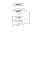
- S11 of FIG. 7 it is determined whether the overcurrent monitoring circuit 44 has detected overcurrent. In the case of YES in S11, the drive circuit 41 turns off the boosting MOS 25 in S12, and continues the off state until the next duty-on timing.
- the overcurrent monitoring circuit 44 counts the number of overcurrent detections for each communication interval with the control unit. In S14, it is determined whether or not the number of times of overcurrent detection has exceeded a predetermined number N times. In the case of YES in S14, the overcurrent monitoring circuit 44 determines that the first condition is met, and transmits an overcurrent flag as a notification signal to the control unit.
- the control unit determines whether the notification signal from the overcurrent monitoring circuit 44 has continued for the determination time or longer. In the case of YES in S26, the control unit determines in S30 that the second condition is satisfied, and determines an abnormality. Subsequently, the control unit performs treatment in S40. In the case of NO in S26, the control unit determines that the second condition is not satisfied.
- the determination time may be set to a time longer than the maximum time of the overcurrent state when the power is turned on or in the overboost mode in the initial check.
- the determination time may be set to a time longer than the maximum time of the overcurrent state when the power is turned on or in the overboost mode in the initial check.
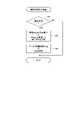
- FIG. 9 shows a process in which the control unit sets the determination time to a different value depending on the situation, or masks the notification signal.
- the power supply voltage corresponding to the pre-relay voltage VLa in FIG. 1 is monitored as the "monitoring voltage”.
- the control unit sets the determination time to a different value according to the operation mode or power supply voltage of the booster 301, or masks the notification signal in a specific operation mode or a specific power supply voltage range.
- the control unit judges an abnormality based on the notification from the overcurrent monitoring circuit 44, the power supply voltage monitoring value, the internal values such as the status code, that is, based on the external and internal information.
- the power supply voltage is equal to or less than a predetermined voltage threshold. As the power supply voltage becomes lower, the step-up ratio becomes larger and a large current flows, so that an erroneous determination is more likely to occur.
- the absolute value of the time rate of change of the power supply voltage is equal to or greater than a predetermined voltage fluctuation threshold, that is, whether the power supply voltage has suddenly fluctuated. For example, when the power supply voltage is interrupted for some reason and then restored, there is a possibility that a large current will flow instantaneously, so erroneous determination is likely to occur.
- the control unit sets the determination time longer than the reference value or masks the notification signal.
- the determination time By setting the determination time longer than the reference value in a specific operation mode or a specific power supply voltage, the second condition is less likely to be satisfied, and erroneous determination can be prevented. Further, by masking the notification signal in a specific operation mode or a specific power supply voltage, the possibility that the second condition is satisfied is eliminated, and erroneous determination is reliably prevented.
- the post-relay voltage VLb or the post-boost voltage VH may be compared with the threshold value as the "monitoring voltage".
- Fig. 10 shows an example of measures to be taken when an abnormality is determined. If the controller determines that there is an abnormality and YES in S41, the controller stops the operation of the booster MOS 25 in S42, or changes the duty ratio to operate the booster MOS 25.
- FIG. FIG. 4 exemplifies a case where the operation of the boost MOS 25 is stopped, but it is possible to change the duty ratio and operate the boost MOS 25 in a restricted manner depending on the state of element failure.
- the microcomputer 50 as a control unit further uses the power of the battery 15 to control the drive of the motor 80 of the electric power steering device 99 .
- the microcomputer 50 may further stop driving the motor 80 or limit the output of the motor 80 in S43 as a measure at the time of abnormality determination. When stopping driving, only the communication of input/output signals used for control may be continued, or the system including the communication system may be shut down.
- the overcurrent monitoring circuit 44 does not judge abnormality merely by detecting overcurrent, but transmits a notification signal to the microcomputer 50 when the first condition is satisfied. Further, the microcomputer 50 determines abnormality for the first time when the second condition is established, and takes measures. Therefore, it is possible to avoid erroneously determining that an overcurrent is abnormal when the power is turned on or when the initial check is performed. Further, when an abnormality is determined due to an element failure or the like, the microcomputer 50 stops the operation of the boosting MOS 25, thereby preventing the PWM operation from being continued in a broken state.
- a soft start circuit is not used, and an overcurrent is detected with respect to an overcurrent threshold set below the rating of the boost MOS 25 at the time of power-on or initial check. Power on while In other words, erroneous determination is prevented by preventing the second condition from being satisfied while assuming that the first condition is likely to be satisfied at the time of power-on or initial check. This simplifies the circuit configuration and shortens the start-up time.
- the microcomputer 50 when the microcomputer 50 receives the notification signal from the overcurrent monitoring circuit 44, in addition to determining whether the notification signal is to be continued based on the determination time, it performs processing such as changing the determination time based on the operation mode, power supply voltage, etc., masking the notification signal, and the like. Abnormalities can be determined in combination and comprehensively. Therefore, it is possible to determine an abnormality and take measures according to the situation. Furthermore, if the design of the determination conditions is changed due to a power supply fluctuation test, constant change of an external element, etc., it will be easier to deal with it by changing the condition settings with software.
- the boost MOS 25, the drive circuit 41 and the overcurrent monitoring circuit 44 are built in the same ASIC 40, so the layout on the substrate is compact.
- the ASIC 40 may be integrated with each function other than the boosting device.
- the microcomputer 50 performs the function of the "control section", it is advantageous in terms of arithmetic processing capability and communication with the outside.
- the drive circuit 42 in the ASIC 40 also functions as a "control section". That is, the notification signal generated when the first condition is established is not transmitted from the overcurrent monitoring circuit 44 of the ASIC 40 to the microcomputer 50, but is transmitted from the overcurrent monitoring circuit 44 to the drive circuit 42 inside the ASIC 40. .
- the drive circuit 42 that has received the notification signal determines whether the second condition is true or not, and when the second condition is satisfied, determines that there is an abnormality, and takes measures. Also, the information on the power supply voltage may be obtained by the drive circuit 42 instead of the microcomputer 50 .
- the effects of the second embodiment can be similarly interpreted by replacing the "microcomputer 50" in the description of the control unit of the first embodiment with the "drive circuit 42".
- the second embodiment does not require the microcomputer 50, so the booster 302 can be configured more simply.
- the operation of the boosting MOS 25 can be immediately stopped without delay in communication when an abnormality is determined, thereby improving reliability.
- the drive circuit 42 and the microcomputer 50 may share the function of the "control section" and cooperate with each other by having the drive circuit 42 also serve as part of the function of the "control section.”
- the "first condition" in the overcurrent monitoring circuit is when the number of overcurrent detections exceeds a predetermined number of times continuously or intermittently at each communication interval with the control unit. It may be established when the current or the integrated value of the current square value exceeds the threshold for each interval.
- the notification signal e.g., overcurrent flag
- the interruption time exceeds a predetermined time
- the timer may be reset.
- the success or failure of the second condition may be determined based on the number of times or frequency of reception of the notification signal within a predetermined period.
- the boost switching element is not limited to a MOSFET, and may be composed of an FET other than MOSFETE or a bipolar transistor.
- the boost switching element, the drive circuit, and the overcurrent monitoring circuit are not limited to being built in the same ASIC 40, but may be mounted directly on the board or built in separate ICs. Also, a capacitor or the like may be used as the "power supply" in addition to the battery 15 .
- the present disclosure is not limited to driving an assist motor of an electric power steering device, but may be used to drive any electric actuator or to output other electrical equipment.
- the controller and techniques described in this disclosure may be implemented by a dedicated computer provided by configuring a processor and memory programmed to perform one or more functions embodied by the computer program.
- the controls and techniques described in this disclosure may be implemented by a dedicated computer provided by configuring the processor with one or more dedicated hardware logic circuits.
- the control units and techniques described in this disclosure can be implemented by a combination of a processor and memory programmed to perform one or more functions and a processor configured by one or more hardware logic circuits. It may also be implemented by one or more dedicated computers configured.
- the computer program may also be stored as computer-executable instructions on a computer-readable non-transitional tangible recording medium.
Landscapes
- Engineering & Computer Science (AREA)
- Power Engineering (AREA)
- Dc-Dc Converters (AREA)
Applications Claiming Priority (2)
| Application Number | Priority Date | Filing Date | Title |
|---|---|---|---|
| JP2021-015790 | 2021-02-03 | ||
| JP2021015790A JP7559590B2 (ja) | 2021-02-03 | 2021-02-03 | 昇圧装置 |
Publications (1)
| Publication Number | Publication Date |
|---|---|
| WO2022168898A1 true WO2022168898A1 (ja) | 2022-08-11 |
Family
ID=82742227
Family Applications (1)
| Application Number | Title | Priority Date | Filing Date |
|---|---|---|---|
| PCT/JP2022/004155 Ceased WO2022168898A1 (ja) | 2021-02-03 | 2022-02-03 | 昇圧装置 |
Country Status (2)
| Country | Link |
|---|---|
| JP (1) | JP7559590B2 (https=) |
| WO (1) | WO2022168898A1 (https=) |
Families Citing this family (1)
| Publication number | Priority date | Publication date | Assignee | Title |
|---|---|---|---|---|
| JP7716034B1 (ja) * | 2025-01-14 | 2025-07-31 | 日新電機株式会社 | 遮断装置および遮断方法 |
Citations (3)
| Publication number | Priority date | Publication date | Assignee | Title |
|---|---|---|---|---|
| JPH06233519A (ja) * | 1993-01-28 | 1994-08-19 | Fuji Electric Co Ltd | 半導体素子の保護回路 |
| JP2007325459A (ja) * | 2006-06-02 | 2007-12-13 | Sony Corp | 電源装置 |
| JP2011030292A (ja) * | 2009-07-22 | 2011-02-10 | Sony Corp | 電源装置 |
-
2021
- 2021-02-03 JP JP2021015790A patent/JP7559590B2/ja active Active
-
2022
- 2022-02-03 WO PCT/JP2022/004155 patent/WO2022168898A1/ja not_active Ceased
Patent Citations (3)
| Publication number | Priority date | Publication date | Assignee | Title |
|---|---|---|---|---|
| JPH06233519A (ja) * | 1993-01-28 | 1994-08-19 | Fuji Electric Co Ltd | 半導体素子の保護回路 |
| JP2007325459A (ja) * | 2006-06-02 | 2007-12-13 | Sony Corp | 電源装置 |
| JP2011030292A (ja) * | 2009-07-22 | 2011-02-10 | Sony Corp | 電源装置 |
Also Published As
| Publication number | Publication date |
|---|---|
| JP2022118936A (ja) | 2022-08-16 |
| JP7559590B2 (ja) | 2024-10-02 |
Similar Documents
| Publication | Publication Date | Title |
|---|---|---|
| US8884559B2 (en) | Motor drive device | |
| JP5743934B2 (ja) | インバータ装置及びパワーステアリング装置 | |
| US9762050B2 (en) | Motor drive device | |
| CN110231560B (zh) | 电感负载控制设备 | |
| US11283389B2 (en) | Motor system | |
| US20190319573A1 (en) | Failure diagnosis method for inverter circuit | |
| US10833614B2 (en) | Motor drive device and electric power steering device | |
| US10840899B2 (en) | Motor drive device and electric power steering device | |
| WO2009125683A1 (ja) | モータ制御装置及びその制御方法 | |
| JP2005329906A (ja) | 電子制御装置,電動パワーステアリング装置,および伝達比可変操舵装置 | |
| US11356036B2 (en) | Power conversion apparatus, motor module, and electric power steering apparatus | |
| WO2020170564A1 (ja) | モータアクチュエータ | |
| WO2021161798A1 (ja) | 電力変換器の制御回路 | |
| US12562666B2 (en) | Actuator driving device and steering system provided with the same | |
| JP5099041B2 (ja) | 燃料ポンプ制御装置 | |
| WO2022168898A1 (ja) | 昇圧装置 | |
| JP7779193B2 (ja) | 負荷駆動装置 | |
| US20080217095A1 (en) | Limiting Device for Limiting Relay Welding and Motor Driving Apparatus | |
| US20220393572A1 (en) | Control circuit for power converter | |
| JP2009159697A (ja) | モータ制御装置 | |
| JP7482014B2 (ja) | モータ駆動制御装置 | |
| CN115280662A (zh) | 电力转换器的控制电路 | |
| CN113044106A (zh) | 电路板 | |
| US20260113027A1 (en) | Semiconductor device | |
| WO2024057878A1 (ja) | モータ制御装置及び電動操舵装置 |
Legal Events
| Date | Code | Title | Description |
|---|---|---|---|
| 121 | Ep: the epo has been informed by wipo that ep was designated in this application |
Ref document number: 22749769 Country of ref document: EP Kind code of ref document: A1 |
|
| NENP | Non-entry into the national phase |
Ref country code: DE |
|
| 122 | Ep: pct application non-entry in european phase |
Ref document number: 22749769 Country of ref document: EP Kind code of ref document: A1 |