WO2022168898A1 - 昇圧装置 - Google Patents
昇圧装置 Download PDFInfo
- Publication number
- WO2022168898A1 WO2022168898A1 PCT/JP2022/004155 JP2022004155W WO2022168898A1 WO 2022168898 A1 WO2022168898 A1 WO 2022168898A1 JP 2022004155 W JP2022004155 W JP 2022004155W WO 2022168898 A1 WO2022168898 A1 WO 2022168898A1
- Authority
- WO
- WIPO (PCT)
- Prior art keywords
- overcurrent
- control unit
- booster
- boosting
- monitoring circuit
- Prior art date
Links
- 238000012544 monitoring process Methods 0.000 claims abstract description 58
- 230000005856 abnormality Effects 0.000 claims abstract description 39
- 238000001514 detection method Methods 0.000 claims description 22
- 238000004891 communication Methods 0.000 claims description 15
- 230000008859 change Effects 0.000 claims description 5
- 230000020169 heat generation Effects 0.000 claims description 4
- 230000009471 action Effects 0.000 claims description 3
- 230000006870 function Effects 0.000 description 12
- 238000000034 method Methods 0.000 description 10
- 239000003990 capacitor Substances 0.000 description 5
- 238000010586 diagram Methods 0.000 description 5
- 230000008569 process Effects 0.000 description 5
- 238000012545 processing Methods 0.000 description 5
- 238000004364 calculation method Methods 0.000 description 3
- 230000002159 abnormal effect Effects 0.000 description 2
- 238000004590 computer program Methods 0.000 description 2
- 230000000694 effects Effects 0.000 description 2
- 230000001939 inductive effect Effects 0.000 description 2
- 230000000873 masking effect Effects 0.000 description 2
- 238000012986 modification Methods 0.000 description 2
- 230000004048 modification Effects 0.000 description 2
- 230000009467 reduction Effects 0.000 description 2
- 239000000758 substrate Substances 0.000 description 2
- 238000009825 accumulation Methods 0.000 description 1
- 230000015556 catabolic process Effects 0.000 description 1
- 238000013461 design Methods 0.000 description 1
- 238000007599 discharging Methods 0.000 description 1
- 238000006073 displacement reaction Methods 0.000 description 1
- 239000004065 semiconductor Substances 0.000 description 1
- 238000004904 shortening Methods 0.000 description 1
- 229910000679 solder Inorganic materials 0.000 description 1
- 238000012360 testing method Methods 0.000 description 1
Images


Classifications
-
- H—ELECTRICITY
- H02—GENERATION; CONVERSION OR DISTRIBUTION OF ELECTRIC POWER
- H02M—APPARATUS FOR CONVERSION BETWEEN AC AND AC, BETWEEN AC AND DC, OR BETWEEN DC AND DC, AND FOR USE WITH MAINS OR SIMILAR POWER SUPPLY SYSTEMS; CONVERSION OF DC OR AC INPUT POWER INTO SURGE OUTPUT POWER; CONTROL OR REGULATION THEREOF
- H02M3/00—Conversion of dc power input into dc power output
- H02M3/02—Conversion of dc power input into dc power output without intermediate conversion into ac
- H02M3/04—Conversion of dc power input into dc power output without intermediate conversion into ac by static converters
- H02M3/10—Conversion of dc power input into dc power output without intermediate conversion into ac by static converters using discharge tubes with control electrode or semiconductor devices with control electrode
- H02M3/145—Conversion of dc power input into dc power output without intermediate conversion into ac by static converters using discharge tubes with control electrode or semiconductor devices with control electrode using devices of a triode or transistor type requiring continuous application of a control signal
- H02M3/155—Conversion of dc power input into dc power output without intermediate conversion into ac by static converters using discharge tubes with control electrode or semiconductor devices with control electrode using devices of a triode or transistor type requiring continuous application of a control signal using semiconductor devices only
Definitions
- the present disclosure relates to a booster.
- An object of the present disclosure is to provide a booster that simplifies the circuit configuration and shortens the start-up time in a booster that prevents erroneous determination of an overcurrent abnormality.
- the present disclosure is a boosting device that boosts and outputs an input power supply voltage.
- This booster includes a boost switching element, a drive circuit, an overcurrent monitoring circuit, and a controller.
- the boost switching element is provided between the ground and the other end of the coil, one end of which is connected to the power supply, and boosts the voltage of the other end of the coil by switching operation.
- the drive circuit PWM-operates the boost switching element.
- the overcurrent monitoring circuit monitors the current flowing through the boost switching element.
- the control unit determines an abnormality based on the notification from the overcurrent monitoring circuit and takes measures.
- the overcurrent monitoring circuit transmits a notification signal to the control unit when the first condition is satisfied regarding the state of the current flowing through the boost switching element.
- the control unit determines that there is an abnormality and takes action.
- the overcurrent monitoring circuit does not make an abnormality determination merely by detecting an overcurrent, and transmits a notification signal to the control unit when the first condition is satisfied. Further, the control unit judges abnormality for the first time when the second condition is established, and takes measures. Therefore, it is possible to avoid erroneously determining that an overcurrent is abnormal when the power is turned on or when the initial check is performed.
- a soft start circuit is not used, and an overcurrent is detected with respect to an overcurrent threshold value set below the rating of the boost switching element at the time of power-on or initial check. power on while In other words, erroneous determination is prevented by preventing the second condition from being satisfied while assuming that the first condition is likely to be satisfied at the time of power-on or initial check. This simplifies the circuit configuration and shortens the start-up time.
- FIG. 1 is a configuration diagram of the booster and its surroundings according to the first embodiment
- FIG. 2 is a schematic configuration diagram of an electric power steering device to which the boost device according to the first embodiment is applied
- FIG. 3 is a circuit diagram showing an overcurrent that occurs when a short circuit fault occurs in a diode or coil
- FIG. 4 is a time chart showing the operation of the boosting device according to the first embodiment
- FIG. 5 is a time chart explaining an example in which the first condition is satisfied
- FIG. 6 is a configuration diagram of an overcurrent detection threshold value setting unit
- FIG. 7 is a flowchart showing the processing when overcurrent is detected
- FIG. 8 is a flowchart of abnormality determination
- FIG. 9 is a flow chart showing a process for preventing erroneous determination
- FIG. 10 is a flow chart showing a procedure when an abnormality is determined
- FIG. 11 is a configuration diagram of the booster and its surroundings according to the second embodiment.
- a booster device boosts a power supply voltage in an electric power steering device for a vehicle.
- the reference numerals of the boosting devices of the first and second embodiments are denoted as "301" and "302", respectively, and the common matters are described as the description of the boosting device 301.
- FIG. 1st Embodiment and 2nd Embodiment differ in the element which functions as a "control part.”
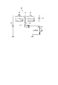
- FIG. 1 shows the configuration of a booster device 301 and its surroundings according to the first embodiment.
- the booster circuit 20 boosts and outputs the power supply voltage input from the battery 15 so that the operation can be continued even when the voltage of the battery 15 is low.
- a voltage before being boosted by the boosting circuit 20 is denoted as VL, and a voltage after being boosted is denoted as VH.
- the inverter 60 also converts the DC power of the battery 15 into AC power and supplies the AC power to the motor 80 .
- Motor 80 is, for example, a three-phase brushless motor.
- the booster circuit 20 is a chopper-type booster circuit including a coil 21, a diode 23, a capacitor 24, and a booster MOS 25 as a "boost switching element".
- the boost MOS 25 is composed of an n-channel MOSFET. In this specification, MOSFET is omitted and simply referred to as "MOS".
- One end of the coil 21 is connected to the battery 15 as a "power supply”. Elements such as a power relay 16 and a diode (not shown) may be connected between the battery 15 and the coil 21 .
- the power relay 16 may be a mechanical relay or a semiconductor switching element.
- the diode 23 has an anode connected to the other end of the coil 21 and a cathode connected to the output terminal.
- a capacitor 24 is provided between the cathode of the diode 23 and the ground.
- the boost MOS 25 is provided between the connection point N at the other end of the coil 21 and the ground. That is, the drain terminal is connected to the connection point N, and the source terminal is grounded. A gate terminal of the boosting MOS 25 is connected to the drive circuit 41 .
- the boost MOS 25 performs switching operation based on the PWM command signal output from the drive circuit 41 .
- the coil 21 repeats accumulation and release of inductive energy, so that the voltage at the other end of the coil 21, that is, the output side is boosted.
- the boosting MOS 25 boosts the voltage on the output side of the coil 21 by switching operation.
- the boosting device 301 of the first embodiment includes at least the boosting MOS 25 among the components of the boosting circuit 20 .
- the booster 301 also includes a drive circuit 41, an overcurrent monitoring circuit 44, and a microcomputer 50 as a "control section".
- the drive circuit 41 causes the boost MOS 25 to perform PWM operation.
- the overcurrent monitoring circuit 44 monitors the current flowing through the boost MOS 25 and detects overcurrent. The technical significance of the overcurrent monitoring circuit 44 will be described later.
- the boost MOS 25, drive circuit 41 and overcurrent monitoring circuit 44 are built in the same IC.
- This IC is referred to herein as an ASIC 40, which stands for Application Specific IC.
- the overcurrent monitoring circuit 44 detects overcurrent, the overcurrent monitoring circuit 44 commands the drive circuit 41 to forcibly turn off the boost MOS 25 as a protection function.
- the ASIC 40 and the microcomputer 50 that constitute the booster 301 communicate with each other.
- the microcomputer 50 determines an abnormality based on the notification from the overcurrent monitoring circuit and takes measures. Specifically, the overcurrent monitoring circuit 44 outputs a notification signal indicating overcurrent detection to the microcomputer 50 .
- the microcomputer 50 instructs the drive circuit 41 to stop the operation of the boost MOS 25, for example, as a measure to be taken when the abnormality is determined.
- the microcomputer 50 monitors a monitoring voltage, which is "a voltage monitored by a circuit before or after boosting". For example, as the voltage of the circuit before boosting, the power supply voltage of the battery 15, that is, the pre-relay voltage VLa on the battery 15 side of the power supply relay 16 in FIG. 1 is monitored. Alternatively, the post-relay voltage VLb between the power relay 16 and the coil 21 may be monitored. Alternatively, the boosted voltage VH, which is the voltage of the circuit after boosting, may be monitored.
- FIG. 2 shows a schematic configuration of a steering system 99 including an electric power steering (denoted as "EPS" in the figure) device 90.
- EPS electric power steering
- the electric power steering device 90 in FIG. 2 is of a column assist type
- the booster device 301 of the present embodiment can also be applied to a rack assist type electric power steering device.
- a steering system 99 includes a steering wheel 91, a steering shaft 92, a steering torque sensor 94, a pinion gear 96, a rack shaft 97, wheels 98, an electric power steering device 90, and the like.
- a pinion gear 96 provided at the tip of the steering shaft 92 meshes with a rack shaft 97 .
- a pair of wheels 98 are provided at both ends of the rack shaft 97 via tie rods or the like.
- a steering torque sensor 94 provided in the middle of the steering shaft 92 detects the steering torque trq. Rotational motion of the steering shaft 92 is converted into linear motion of the rack shaft 97 by the pinion gear 96 , and the pair of wheels 98 are steered at an angle corresponding to the amount of displacement of the rack shaft 97 .
- the electric power steering device 90 includes a boost device 301, an inverter 60, a motor 80, a reduction gear 89, and the like.
- the microcomputer 50 which is one element of the booster device 301 also functions as a motor control device in the electric power steering device 90 .
- the microcomputer 50 as a motor control device acquires information such as the steering torque trq, the steering speed, and the vehicle speed from the outside, and drives the motor 80 so that the motor 80 outputs the desired assist torque calculated from these information. Control.
- the assist torque output by the motor 80 is transmitted to the steering shaft 92 via the reduction gear 89 .
- the present embodiment aims at simplifying the circuit configuration and shortening the start-up time in a booster device that prevents erroneous determination of an overcurrent abnormality.
- the time chart in FIG. 4 shows the overcurrent detection notification operation by the overcurrent monitoring circuit 44 .
- a communication interval from the overcurrent monitoring circuit 44 to the microcomputer 50 is set to 1 ms, for example.
- the drive circuit 41 performs the switching operation of the boost MOS 25 at a PWM cycle of 5 ms, ie, a frequency of 200 kHz, for example. Therefore, the boosting MOS 25 is turned on and off 200 times during the communication interval of 1 ms.
- the duty ratio is expressed by "Ton/T", where Ton is the ON time of the boosting MOS 25 in one PWM period T, and Toff is the OFF time.
- Ton is the ON time of the boosting MOS 25 in one PWM period T
- Toff is the OFF time.
- the duty ratio is calculated according to the boost output target value, and the PWM command signal is generated.
- FIG. 5 shows the command signal when the duty ratio is approximately 50%.
- An overcurrent threshold used for overcurrent detection by the overcurrent monitoring circuit 44 is set for the current when the boost MOS 25 is turned on.
- the overcurrent threshold is set below the breakdown resistance, mainly based on the rating of the boost MOS 25 and the solder reliability of substrate mounting. Also, the overcurrent threshold may be variably set according to the heat generation of the boost MOS 25 .
- the overcurrent threshold calculation unit 43 provided in the ASIC 40 calculates the overcurrent threshold according to the current heat generation of the boost MOS 25 and outputs it to the overcurrent monitoring circuit 44 .
- Heat generation of the boost MOS 25 may be detected by a temperature sensor, or may be estimated by adding Joule heat calculated from a current squared value or the like to the initial temperature. For example, the greater the heat generated by the booster MOS 25, the lower the overcurrent threshold, thereby facilitating overcurrent detection.
- the overcurrent monitoring circuit 44 counts the number of overcurrent detections for each communication interval. As shown in FIG. 5, each time the overcurrent monitoring circuit 44 detects an overcurrent, the drive circuit 41 forcibly turns off the boost MOS 25 and continues the off state until the next duty-on timing. Therefore, in the switch operation at the time of overcurrent detection, the ON time is shortened by the time indicated by the two-dot chain line with respect to the PWM command signal. Since the boost MOS 25 is forcibly turned off, the current becomes 0. As long as the cause of the overcurrent continues, the current becomes equal to or greater than the overcurrent threshold again in the next duty-on period, and the overcurrent is detected.
- the overcurrent state occurs temporarily after the boost operation permission signal is turned on. During that period, the overcurrent monitoring circuit 44 counts the number of overcurrent detections for each communication interval. Then, when the number of times of overcurrent detection for each communication interval exceeds a predetermined number of times, N times, the overcurrent monitoring circuit 44 determines that the state of the current flowing through the boosting MOS 25 has satisfied the first condition, and notifies An overcurrent flag is output as a signal. On the other hand, when the boost operation permission signal is off before the start of the boost operation or after the temporary overcurrent state ends, the number of overcurrent detections per communication interval becomes N times or less, and the overcurrent flag is not output. .
- the count of the number of times of overcurrent detection is not limited to the case where overcurrent is detected continuously every cycle as shown in [Example 1] of FIG. Even if the current is not detected, the total number of times should be counted. In addition to the case where the current actually falls below the threshold value as shown in [Example 2], it also includes the case where the current reaches the threshold value but fails to count due to a detection error. In short, the overcurrent flag is output when the total number of overcurrent detections for each communication interval exceeds N times, regardless of whether it is continuous or discontinuous.
- the microcomputer 50 of the first embodiment is generalized and referred to as a "controller". Therefore, the same flowchart and the same description are used in the second embodiment.
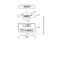
- S11 of FIG. 7 it is determined whether the overcurrent monitoring circuit 44 has detected overcurrent. In the case of YES in S11, the drive circuit 41 turns off the boosting MOS 25 in S12, and continues the off state until the next duty-on timing.
- the overcurrent monitoring circuit 44 counts the number of overcurrent detections for each communication interval with the control unit. In S14, it is determined whether or not the number of times of overcurrent detection has exceeded a predetermined number N times. In the case of YES in S14, the overcurrent monitoring circuit 44 determines that the first condition is met, and transmits an overcurrent flag as a notification signal to the control unit.
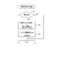
- the control unit determines whether the notification signal from the overcurrent monitoring circuit 44 has continued for the determination time or longer. In the case of YES in S26, the control unit determines in S30 that the second condition is satisfied, and determines an abnormality. Subsequently, the control unit performs treatment in S40. In the case of NO in S26, the control unit determines that the second condition is not satisfied.
- the determination time may be set to a time longer than the maximum time of the overcurrent state when the power is turned on or in the overboost mode in the initial check.
- the determination time may be set to a time longer than the maximum time of the overcurrent state when the power is turned on or in the overboost mode in the initial check.
- FIG. 9 shows a process in which the control unit sets the determination time to a different value depending on the situation, or masks the notification signal.
- the power supply voltage corresponding to the pre-relay voltage VLa in FIG. 1 is monitored as the "monitoring voltage”.
- the control unit sets the determination time to a different value according to the operation mode or power supply voltage of the booster 301, or masks the notification signal in a specific operation mode or a specific power supply voltage range.
- the control unit judges an abnormality based on the notification from the overcurrent monitoring circuit 44, the power supply voltage monitoring value, the internal values such as the status code, that is, based on the external and internal information.
- the power supply voltage is equal to or less than a predetermined voltage threshold. As the power supply voltage becomes lower, the step-up ratio becomes larger and a large current flows, so that an erroneous determination is more likely to occur.
- the absolute value of the time rate of change of the power supply voltage is equal to or greater than a predetermined voltage fluctuation threshold, that is, whether the power supply voltage has suddenly fluctuated. For example, when the power supply voltage is interrupted for some reason and then restored, there is a possibility that a large current will flow instantaneously, so erroneous determination is likely to occur.
- the control unit sets the determination time longer than the reference value or masks the notification signal.
- the determination time By setting the determination time longer than the reference value in a specific operation mode or a specific power supply voltage, the second condition is less likely to be satisfied, and erroneous determination can be prevented. Further, by masking the notification signal in a specific operation mode or a specific power supply voltage, the possibility that the second condition is satisfied is eliminated, and erroneous determination is reliably prevented.
- the post-relay voltage VLb or the post-boost voltage VH may be compared with the threshold value as the "monitoring voltage".
- Fig. 10 shows an example of measures to be taken when an abnormality is determined. If the controller determines that there is an abnormality and YES in S41, the controller stops the operation of the booster MOS 25 in S42, or changes the duty ratio to operate the booster MOS 25.
- FIG. FIG. 4 exemplifies a case where the operation of the boost MOS 25 is stopped, but it is possible to change the duty ratio and operate the boost MOS 25 in a restricted manner depending on the state of element failure.
- the microcomputer 50 as a control unit further uses the power of the battery 15 to control the drive of the motor 80 of the electric power steering device 99 .
- the microcomputer 50 may further stop driving the motor 80 or limit the output of the motor 80 in S43 as a measure at the time of abnormality determination. When stopping driving, only the communication of input/output signals used for control may be continued, or the system including the communication system may be shut down.
- the overcurrent monitoring circuit 44 does not judge abnormality merely by detecting overcurrent, but transmits a notification signal to the microcomputer 50 when the first condition is satisfied. Further, the microcomputer 50 determines abnormality for the first time when the second condition is established, and takes measures. Therefore, it is possible to avoid erroneously determining that an overcurrent is abnormal when the power is turned on or when the initial check is performed. Further, when an abnormality is determined due to an element failure or the like, the microcomputer 50 stops the operation of the boosting MOS 25, thereby preventing the PWM operation from being continued in a broken state.
- a soft start circuit is not used, and an overcurrent is detected with respect to an overcurrent threshold set below the rating of the boost MOS 25 at the time of power-on or initial check. Power on while In other words, erroneous determination is prevented by preventing the second condition from being satisfied while assuming that the first condition is likely to be satisfied at the time of power-on or initial check. This simplifies the circuit configuration and shortens the start-up time.
- the microcomputer 50 when the microcomputer 50 receives the notification signal from the overcurrent monitoring circuit 44, in addition to determining whether the notification signal is to be continued based on the determination time, it performs processing such as changing the determination time based on the operation mode, power supply voltage, etc., masking the notification signal, and the like. Abnormalities can be determined in combination and comprehensively. Therefore, it is possible to determine an abnormality and take measures according to the situation. Furthermore, if the design of the determination conditions is changed due to a power supply fluctuation test, constant change of an external element, etc., it will be easier to deal with it by changing the condition settings with software.
- the boost MOS 25, the drive circuit 41 and the overcurrent monitoring circuit 44 are built in the same ASIC 40, so the layout on the substrate is compact.
- the ASIC 40 may be integrated with each function other than the boosting device.
- the microcomputer 50 performs the function of the "control section", it is advantageous in terms of arithmetic processing capability and communication with the outside.
- the drive circuit 42 in the ASIC 40 also functions as a "control section". That is, the notification signal generated when the first condition is established is not transmitted from the overcurrent monitoring circuit 44 of the ASIC 40 to the microcomputer 50, but is transmitted from the overcurrent monitoring circuit 44 to the drive circuit 42 inside the ASIC 40. .
- the drive circuit 42 that has received the notification signal determines whether the second condition is true or not, and when the second condition is satisfied, determines that there is an abnormality, and takes measures. Also, the information on the power supply voltage may be obtained by the drive circuit 42 instead of the microcomputer 50 .
- the effects of the second embodiment can be similarly interpreted by replacing the "microcomputer 50" in the description of the control unit of the first embodiment with the "drive circuit 42".
- the second embodiment does not require the microcomputer 50, so the booster 302 can be configured more simply.
- the operation of the boosting MOS 25 can be immediately stopped without delay in communication when an abnormality is determined, thereby improving reliability.
- the drive circuit 42 and the microcomputer 50 may share the function of the "control section" and cooperate with each other by having the drive circuit 42 also serve as part of the function of the "control section.”
- the "first condition" in the overcurrent monitoring circuit is when the number of overcurrent detections exceeds a predetermined number of times continuously or intermittently at each communication interval with the control unit. It may be established when the current or the integrated value of the current square value exceeds the threshold for each interval.
- the notification signal e.g., overcurrent flag
- the interruption time exceeds a predetermined time
- the timer may be reset.
- the success or failure of the second condition may be determined based on the number of times or frequency of reception of the notification signal within a predetermined period.
- the boost switching element is not limited to a MOSFET, and may be composed of an FET other than MOSFETE or a bipolar transistor.
- the boost switching element, the drive circuit, and the overcurrent monitoring circuit are not limited to being built in the same ASIC 40, but may be mounted directly on the board or built in separate ICs. Also, a capacitor or the like may be used as the "power supply" in addition to the battery 15 .
- the present disclosure is not limited to driving an assist motor of an electric power steering device, but may be used to drive any electric actuator or to output other electrical equipment.
- the controller and techniques described in this disclosure may be implemented by a dedicated computer provided by configuring a processor and memory programmed to perform one or more functions embodied by the computer program.
- the controls and techniques described in this disclosure may be implemented by a dedicated computer provided by configuring the processor with one or more dedicated hardware logic circuits.
- the control units and techniques described in this disclosure can be implemented by a combination of a processor and memory programmed to perform one or more functions and a processor configured by one or more hardware logic circuits. It may also be implemented by one or more dedicated computers configured.
- the computer program may also be stored as computer-executable instructions on a computer-readable non-transitional tangible recording medium.
Landscapes
- Engineering & Computer Science (AREA)
- Power Engineering (AREA)
- Dc-Dc Converters (AREA)
Abstract
昇圧装置の昇圧スイッチング素子(25)は、電源(15)に一端が接続されたコイル(21)の他端とグランドとの間に設けられ、スイッチング動作によりコイル(21)の他端の電圧を昇圧する。ドライブ回路(41)は、昇圧スイッチング素子(25)をPWM動作させる。過電流監視回路(44)は、昇圧スイッチング素子(25)に流れる電流を監視する。制御部(50)は、過電流監視回路(44)からの通知に基づき異常判定し、処置を行う。過電流監視回路(44)は、昇圧スイッチング素子(25)に流れる電流の状態について第1条件が成立したとき、制御部(50)に通知信号を送信する。制御部(50)は、過電流監視回路(44)から受信した通知信号について第2条件が成立したとき、異常判定し、処置を行う。
Description
本出願は、2021年2月3日に出願された特許出願番号2021-015790号に基づくものであり、ここにその記載内容を援用する。
本開示は、昇圧装置に関する。
従来、入力された電源電圧を昇圧して出力する昇圧装置が知られている。また、過電流を検出したとき異常判定し動作を停止する過電流保護回路において、電源投入時等の一時的な過電流による誤判定を防止する技術が知られている。例えば特許文献1に開示されたスイッチングレギュレータは、過電流が検出されたとき、ソフトスタート回路のコンデンサをディスチャージすることで電流を制限している。
特許文献1のスイッチングレギュレータでは、ソフトスタート回路を用いるため、回路構成が複雑になり、電源投入時の立ち上げ時間が長くかかる。
本開示の目的は、過電流異常の誤判定を防止する昇圧装置において、回路構成を簡素化し、立ち上げ時間を短縮する昇圧装置を提供することにある。
本開示は、入力された電源電圧を昇圧して出力する昇圧装置である。この昇圧装置は、昇圧スイッチング素子と、ドライブ回路と、過電流監視回路と、制御部とを備える。
昇圧スイッチング素子は、電源に一端が接続されたコイルの他端とグランドとの間に設けられ、スイッチング動作によりコイルの他端の電圧を昇圧する。ドライブ回路は、昇圧スイッチング素子をPWM動作させる。過電流監視回路は、昇圧スイッチング素子に流れる電流を監視する。制御部は、過電流監視回路からの通知に基づき異常判定し、処置を行う。
過電流監視回路は、昇圧スイッチング素子に流れる電流の状態について第1条件が成立したとき、制御部に通知信号を送信する。制御部は、過電流監視回路から受信した通知信号について第2条件が成立したとき、異常判定し、処置を行う。
本開示では、過電流監視回路が過電流検出しただけでは異常判定せず、第1条件が成立したとき制御部に通知信号を送信する。制御部は、さらに第2条件が成立したときに初めて異常判定し、処置を行う。したがって、電源投入時やイニシャルチェック時の過電流に対し、異常と誤判定することが回避される。
また本開示では、特許文献1の従来技術のようにソフトスタート回路を用いず、電源投入時やイニシャルチェック時には、昇圧スイッチング素子の定格以下に設定された過電流閾値に対して過電流を検出しながら通電する。つまり、電源投入時やイニシャルチェック時には第1条件が成立する可能性が高いことを前提としつつ、第2条件が成立しないようにすることで誤判定を防止する。これにより、回路構成を簡素化し、立ち上げ時間を短縮することができる。
本開示についての上記目的及びその他の目的、特徴や利点は、添付の図面を参照しながら下記の詳細な記述により、より明確になる。その図面は、
図1は、第1実施形態による昇圧装置及び周辺の構成図であり、
図2は、第1実施形態による昇圧装置が適用される電動パワーステアリング装置の概略構成図であり、
図3は、ダイオード又はコイルのショート故障時に発生する過電流を示す回路図であり、
図4は、第1実施形態による昇圧装置の動作を示すタイムチャートであり、
図5は、第1条件が成立する例を説明するタイムチャートであり、
図6は、過電流検出閾値設定部の構成図であり、
図7は、過電流検出時の処理を示すフローチャートであり、
図8は、異常判定のフローチャートであり、
図9は、誤判定防止の処理を示すフローチャートであり、
図10は、異常判定時の処置を示すフローチャートであり、
図11は、第2実施形態による昇圧装置及び周辺の構成図である。
以下、昇圧装置の複数の実施形態を、図面に基づいて説明する。第1及び第2実施形態を包括して「本実施形態」という。本実施形態の昇圧装置は、車両の電動パワーステアリング装置において電源電圧を昇圧する。第1、第2実施形態の昇圧装置の符号をそれぞれ「301」、「302」と記し、共通する事項については昇圧装置301の説明として記載する。第1実施形態及び第2実施形態は、「制御部」として機能する要素が異なる。
(第1実施形態)
図1に、第1実施形態の昇圧装置301及び周辺の構成を示す。昇圧回路20は、バッテリ15の低電圧時にも動作を継続できるようにするため、バッテリ15から入力された電源電圧を昇圧して出力する。昇圧回路20による昇圧前の電圧をVL、昇圧後の電圧をVHと記す。また、インバータ60は、バッテリ15の直流電力を交流電力に変換し、モータ80に供給する。モータ80は、例えば3相ブラシレスモータである。
図1に、第1実施形態の昇圧装置301及び周辺の構成を示す。昇圧回路20は、バッテリ15の低電圧時にも動作を継続できるようにするため、バッテリ15から入力された電源電圧を昇圧して出力する。昇圧回路20による昇圧前の電圧をVL、昇圧後の電圧をVHと記す。また、インバータ60は、バッテリ15の直流電力を交流電力に変換し、モータ80に供給する。モータ80は、例えば3相ブラシレスモータである。
昇圧回路20は、コイル21、ダイオード23、コンデンサ24、及び、「昇圧スイッチング素子」としての昇圧MOS25を含む、チョッパ式の昇圧回路である。昇圧MOS25は、nチャネル型MOSFETで構成されている。なお、本明細書ではMOSFETを省略し、単に「MOS」と記す。
コイル21は、一端が「電源」としてのバッテリ15に接続されている。バッテリ15とコイル21との間には、電源リレー16や、図示しないダイオード等の素子が接続されてもよい。電源リレー16は機械式リレーでも半導体スイッチング素子でもよい。ダイオード23は、アノードがコイル21の他端に接続され、カソードが出力端に接続されている。コンデンサ24は、ダイオード23のカソードとグランドとの間に設けられている。
昇圧MOS25は、コイル21の他端における接続点Nとグランドとの間に設けられている。つまり、ドレイン端子が接続点Nに接続され、ソース端子が接地されている。昇圧MOS25のゲート端子はドライブ回路41に接続されている。昇圧MOS25は、ドライブ回路41から出力されるPWM指令信号に基づいてスイッチング動作する。これに伴い、コイル21が誘導エネルギーの蓄積と放出とを繰り返すことで、コイル21の他端、すなわち出力側の電圧が昇圧される。要するに昇圧MOS25は、スイッチング動作により、コイル21の出力側の電圧を昇圧する。
第1実施形態の昇圧装置301は、昇圧回路20の構成要素のうち少なくとも昇圧MOS25を備える。また、昇圧装置301は、ドライブ回路41、過電流監視回路44、及び、「制御部」としてのマイコン50を備える。ドライブ回路41は、昇圧MOS25をPWM動作させる。過電流監視回路44は、昇圧MOS25に流れる電流を監視し、過電流を検出する。過電流監視回路44の技術的意義については後述する。
昇圧MOS25、ドライブ回路41及び過電流監視回路44は、同一のICに内蔵されている。本明細書では、このICを、特定用途向けICを意味するASIC40と記す。過電流監視回路44が過電流検出したとき、保護機能として、過電流監視回路44はドライブ回路41に対し昇圧MOS25の強制オフを指令する。昇圧装置301を構成するASIC40とマイコン50とは互いに通信する。マイコン50は、過電流監視回路からの通知に基づき異常判定し、処置を行う。詳しくは、過電流監視回路44からマイコン50に対し、過電流検出を示す通知信号が出力される。
またマイコン50は、異常判定時の処置として、ドライブ回路41に対し、例えば昇圧MOS25の動作停止を指令する。さらにマイコン50は、「昇圧前もしくは昇圧後の回路で監視される電圧」である監視電圧を監視する。例えば、昇圧前の回路の電圧として、バッテリ15の電源電圧、すなわち、図1における電源リレー16よりもバッテリ15側のリレー前電圧VLaが監視される。或いは、電源リレー16とコイル21との間のリレー後電圧VLbが監視されてもよい。或いは、昇圧後の回路の電圧である昇圧後電圧VHが監視されてもよい。
図2に、電動パワーステアリング(図中「EPS」と記す)装置90を含むステアリングシステム99の概略構成を示す。なお、図2の電動パワーステアリング装置90はコラムアシスト式であるが、本実施形態の昇圧装置301は、ラックアシスト式の電動パワーステアリング装置にも同様に適用可能である。ステアリングシステム99は、ハンドル91、ステアリングシャフト92、操舵トルクセンサ94、ピニオンギア96、ラック軸97、車輪98、及び、電動パワーステアリング装置90等を含む。
ステアリングシャフト92の先端に設けられたピニオンギア96は、ラック軸97に噛み合っている。ラック軸97の両端には、タイロッド等を介して一対の車輪98が設けられる。運転者がハンドル91を回転させると、ハンドル91に接続されたステアリングシャフト92が回転する。ステアリングシャフト92の途中に設けられた操舵トルクセンサ94は、操舵トルクtrqを検出する。ステアリングシャフト92の回転運動は、ピニオンギア96によりラック軸97の直線運動に変換され、ラック軸97の変位量に応じた角度に一対の車輪98が操舵される。
電動パワーステアリング装置90は、昇圧装置301、インバータ60、モータ80、減速ギア89等を含む。本実施形態では昇圧装置301の一要素であるマイコン50は、電動パワーステアリング装置90におけるモータ制御装置としても機能する。モータ制御装置としてのマイコン50は、操舵トルクtrqや操舵速度、車速等の情報を外部から取得し、これらの情報から演算される所望のアシストトルクをモータ80が出力するようにモータ80の駆動を制御する。モータ80が出力したアシストトルクは、減速ギア89を介してステアリングシャフト92に伝達される。
次に図3を参照し、昇圧回路20の素子故障によって生じる過電流異常の発生例について説明する。コイル21がショート故障すると、バッテリ15の電力が誘導エネルギーに変換されることなく昇圧MOS25に直接印加され、昇圧MOS25のオン時、一点鎖線矢印で示すように過電流が流れる。ダイオード23がショート故障すると、コンデンサ24から放電された電流がダイオード23を逆流し、昇圧MOS25のオン時、二点鎖線矢印で示すように、昇圧MOS25に過電流が流れる。これにより、昇圧MOS25が破壊されるおそれがある。
このような場合に昇圧MOS25を保護するため、過電流を検出し、異常の場合に通電停止等の処置を取ることが求められる。しかし一方、電源投入時等には回路が正常であっても一時的に過電流が検出される場合があり、誤って異常と判定することを防止することが求められる。
ただし、特許文献1(特開2014-3850号公報)の従来技術のようにソフトスタート回路を用いると、回路構成が複雑になり、電源投入時の立ち上げ時間が長くかかる。そこで本実施形態は、過電流異常の誤判定を防止する昇圧装置において、回路構成を簡素化し、立ち上げ時間を短縮することを目的とするものである。
次に図4~図10を参照し、本実施形態による過電流検出から異常判定時の処置までの一連の処理について説明する。図7~図10のフローチャートの説明で記号「S」はステップを示す。
図4のタイムチャートには、過電流監視回路44による過電流検出の通知動作を示す。過電流監視回路44からマイコン50への通信間隔は、例えば1msに設定されている。昇圧動作許可信号がオンのとき、ドライブ回路41は昇圧MOS25を例えばPWM周期5ms、すなわち周波数200kHzでスイッチング動作する。したがって、昇圧MOS25は通信間隔1ms中に200回オンオフ動作する。
図5に示すように、PWM一周期Tにおける昇圧MOS25のオン時間をTon、オフ時間をToffとすると、duty比は、「Ton/T」で表される。昇圧装置301の通常動作時には、昇圧出力目標値に応じてduty比が演算され、PWM指令信号が生成される。図5には、duty比が約50%の場合の指令信号を図示する。
昇圧MOS25のオン時の電流に対し、過電流監視回路44の過電流検出に用いられる過電流閾値が設定される。過電流閾値は、主に昇圧MOS25の定格や基板実装のはんだ信頼性に基づき、破壊耐量以下で設定される。また過電流閾値は、昇圧MOS25の発熱に応じて可変に設定されてもよい。
例えば図6に示す構成では、ASIC40内に設けられた過電流閾値演算部43が現在の昇圧MOS25の発熱に応じて過電流閾値を演算し、過電流監視回路44に出力する。昇圧MOS25の発熱は温度センサにより検出されてもよいし、電流二乗値等から算出されたジュール熱を初期温度に加算して推定されてもよい。例えば昇圧MOS25の発熱が大きいほど過電流閾値を低くして過電流検出されやすくすることで、昇圧MOS25をより過熱から保護する方向に調整される。
過電流監視回路44は、通信間隔ごとに過電流検出回数をカウントする。図5に示すように、過電流監視回路44が過電流検出するごとに、ドライブ回路41は昇圧MOS25を強制的にオフし、次のdutyオンタイミングまでオフ状態を継続する。したがって、過電流検出時のスイッチ動作では、PWM指令信号に対し二点鎖線で示す時間だけ、オン時間が短くなる。昇圧MOS25が強制的にオフされるため、電流は0になる。そして、過電流の要因が続く限り、次のdutyオン期間に再び電流が過電流閾値以上となり、過電流検出される。
例えば、昇圧装置301の電源投入時やイニシャルチェックでの過昇圧モード時には、昇圧動作許可信号がオンされた後、一時的に過電流状態となる。その期間、過電流監視回路44は、通信間隔ごとに過電流検出回数をカウントする。そして、通信間隔ごとの過電流検出回数が所定回数であるN回を超えたとき、過電流監視回路44は、昇圧MOS25に流れる電流の状態について「第1条件が成立した」と判断し、通知信号として過電流フラグを出力する。一方、昇圧動作の開始前で昇圧動作許可信号がオフのときや、一時的な過電流状態が終了した後には、通信間隔ごとの過電流検出回数がN回以下となり、過電流フラグは出力されない。
ここで、過電流検出回数のカウントは、図5の[例1]に示すように、毎周期連続して過電流検出される場合に限らず、[例2]に示すように、途中に過電流検出されない場合があっても、合計回数がカウントされればよい。[例2]に図示するように実際に電流が閾値以下となった場合の他、電流が閾値に達したにもかかわらず、検出のエラーによってカウントし損なった場合等も含まれる。要するに、連続か不連続かに関係なく、通信間隔ごとの過電流検出回数の合計がN回を超えたとき、過電流フラグが出力される。
その後、時刻txにコイル、ダイオード等の素子がショート故障し、恒久的な過電流異常(すなわち真性異常)の状態になると仮定する。それ以後は常に過電流が検出され、通信間隔ごとの過電流検出回数の合計がN回を超えて、過電流フラグが出力される。マイコン50は、過電流監視回路44から受信した過電流フラグについて、過電流フラグが所定の判定時間以上継続したとき、「第2条件が成立した」と判断し、異常判定する。そしてマイコン50は、異常判定時の処置として、昇圧動作許可信号をオンからオフに変更し、昇圧MOS25の動作を停止する。
図7、図8のフローチャートに上記処理の基本的な流れを示す。フローチャート、及び以下のフローチャートに関する説明では、第1実施形態のマイコン50を一般化して「制御部」と記す。したがって、第2実施形態でも同じフローチャート及び同じ説明が援用される。図7のS11では、過電流監視回路44が過電流検出したか判断される。S11でYESの場合、S12でドライブ回路41は昇圧MOS25をオフし、次のdutyオンタイミングまでオフ状態を継続する。
図8のS13で過電流監視回路44は、制御部との通信間隔ごとに過電流検出回数をカウントする。S14では過電流検出回数が所定回数N回を超えたか判断される。S14でYESの場合、過電流監視回路44は、第1条件が成立したと判断し、制御部に通知信号として過電流フラグを送信する。
S26で制御部は、過電流監視回路44からの通知信号が判定時間以上継続したか判断する。S26でYESの場合、S30で制御部は、第2条件が成立したと判断し、異常判定する。続いて制御部は、S40で処置を行う。S26でNOの場合、制御部は、第2条件が成立しないと判断する。
第2条件の判定において、例えば判定時間は、電源投入時やイニシャルチェックでの過昇圧モード時における過電流状態の最大時間よりも長い時間に設定されてもよい。これにより、電源投入時やイニシャルチェックでの過昇圧モード時には第1条件は成立しても第2条件が不成立となるため、異常と誤判定されることが防止される。或いは、電源投入時等の状況に応じて制御部が異常判定の処理を変更することで、誤判定を防止してもよい。次に図9を参照し、誤判定防止の処理例について説明する。
図9には、制御部が、状況に応じて判定時間を異なる値に設定するか、或いは、通知信号をマスクする処理を示す。ここでは、図1のリレー前電圧VLaに相当する電源電圧が「監視電圧」として監視されるものとして説明する。具体的に制御部は、昇圧装置301の動作モードもしくは電源電圧に応じて判定時間を異なる値に設定するか、或いは、特定の動作モードもしくは特定の電源電圧の範囲で通知信号をマスクする。このように制御部は、過電流監視回路44からの通知、電源電圧監視値、状態コード等の内部値を併せて、すなわち外部及び内部の情報に基づき異常判定する。
図9のS21からS24では、「特定の動作モードもしくは特定の監視電圧」に関する4つの判断項目について順に成否が判断される。これらの判断順序は任意である。S21では、昇圧装置301の電源投入時であるか判断される。一般に電源投入時には突入電流による誤判定が生じやすくなる。
S22では、起動時に回路の異常を診断するイニシャルチェックにおいて、昇圧出力目標値を一時的に上げるときであるか判断される。イニシャルチェックでは昇圧出力目標値を通常時の値よりも高くして昇圧機能が正常であることを診断するため、誤判定が生じやすくなる。
S23では、電源電圧が所定の電圧閾値以下であるか判断される。電源電圧が低いときほど昇圧比が大きくなり、大電流が流れるため、誤判定が生じやすくなる。S24では、電源電圧の時間変化率の絶対値が所定の電圧変動閾値以上であるか、つまり、電源電圧が急変動したか判断される。例えば何らかの要因で電源電圧が途絶した後に復帰したとき、瞬時に大電流が流れる可能性があるため、誤判定が生じやすくなる。
S21~S24のいずれかでYESの場合、S25で制御部は、判定時間を基準値よりも長く設定するか、或いは、通知信号をマスクする。特定の動作モードもしくは特定の電源電圧において判定時間を基準値よりも長く設定することで、第2条件が成立しにくくなり、誤判定を防止することができる。また、特定の動作モードもしくは特定の電源電圧において通知信号をマスクすることで、第2条件の成立の可能性が無くなり、誤判定が確実に防止される。なお、S23、S24では、リレー前の電源電圧VLaに代えて、リレー後電圧VLbや昇圧後電圧VHが「監視電圧」として閾値と比較されてもよい。
図10に、異常判定時の処置例を示す。制御部が異常判定し、S41でYESの場合、制御部は、S42で昇圧MOS25の動作を停止するか、又は、duty比を変更して昇圧MOS25を動作させる。図4には昇圧MOS25の動作を停止する場合が例示されているが、素子故障の状況によっては、duty比を変更して昇圧MOS25制限的に動作させることも可能である。
制御部としてのマイコン50は、さらにバッテリ15の電力を用いて電動パワーステアリング装置99のモータ80の駆動を制御する。マイコン50は、異常判定時の処置として、さらにS43でモータ80の駆動を停止するか、又は、モータ80の出力を制限してもよい。駆動を停止する場合、制御に用いる入出力信号の通信のみは継続してもよいし、通信系も含めてシステムをシャットダウンしてもよい。
(第1実施形態の作用効果)
以上のように第1実施形態では、過電流監視回路44が過電流検出しただけでは異常判定せず、第1条件が成立したときマイコン50に通知信号を送信する。マイコン50は、さらに第2条件が成立したときに初めて異常判定し、処置を行う。したがって、電源投入時やイニシャルチェック時の過電流に対し、異常と誤判定することが回避される。また、素子故障等により異常判定した場合、マイコン50が昇圧MOS25の動作を停止させることで、壊れた状態のままPWM動作を続けることを防止することができる。
以上のように第1実施形態では、過電流監視回路44が過電流検出しただけでは異常判定せず、第1条件が成立したときマイコン50に通知信号を送信する。マイコン50は、さらに第2条件が成立したときに初めて異常判定し、処置を行う。したがって、電源投入時やイニシャルチェック時の過電流に対し、異常と誤判定することが回避される。また、素子故障等により異常判定した場合、マイコン50が昇圧MOS25の動作を停止させることで、壊れた状態のままPWM動作を続けることを防止することができる。
また第1実施形態では、特許文献1の従来技術のようにソフトスタート回路を用いず、電源投入時やイニシャルチェック時には、昇圧MOS25の定格以下に設定された過電流閾値に対して過電流を検出しながら通電する。つまり、電源投入時やイニシャルチェック時には第1条件が成立する可能性が高いことを前提としつつ、第2条件が成立しないようにすることで誤判定を防止する。これにより、回路構成を簡素化し、立ち上げ時間を短縮することができる。
さらに、マイコン50が過電流監視回路44から通知信号を受信したとき、判定時間による通知信号の継続判定に加え、動作モードや電源電圧等に基づく判定時間の変更や通知信号のマスク等の処理を組み合わせ、総合的に異常判定することができる。したがって、状況に応じた異常判定や処置が可能となる。さらに、電源変動試験や外付け素子の定数変更等により判定条件を設計変更した場合等、ソフトウァアで条件設定を変更することで、対応が容易になる。
加えて第1実施形態では、昇圧MOS25、ドライブ回路41及び過電流監視回路44が同一のASIC40に内蔵されているため、基板上のレイアウトがコンパクトになる。なお、ASIC40には昇圧装置以外の各機能が統合されてもよい。また、「制御部」の機能をマイコン50が担っているため、演算処理能力や外部との通信の点で有利である。
(第2実施形態)
次に図11を参照し、第2実施形態について説明する。第2実施形態の昇圧装置302では、ASIC40内のドライブ回路42が「制御部」としての機能を兼ねる。つまり、第1条件が成立したとき生成された通知信号は、ASIC40の過電流監視回路44からマイコン50に送信されるのでなく、ASIC40の内部で過電流監視回路44からドライブ回路42に送信される。通知信号を受信したドライブ回路42は、第2条件の成否を判定し、第2条件が成立したとき異常判定し、処置を行う。また、電源電圧の情報もマイコン50に代わってドライブ回路42が取得してもよい。
次に図11を参照し、第2実施形態について説明する。第2実施形態の昇圧装置302では、ASIC40内のドライブ回路42が「制御部」としての機能を兼ねる。つまり、第1条件が成立したとき生成された通知信号は、ASIC40の過電流監視回路44からマイコン50に送信されるのでなく、ASIC40の内部で過電流監視回路44からドライブ回路42に送信される。通知信号を受信したドライブ回路42は、第2条件の成否を判定し、第2条件が成立したとき異常判定し、処置を行う。また、電源電圧の情報もマイコン50に代わってドライブ回路42が取得してもよい。
第2実施形態の作用効果は、第1実施形態の制御部に関する説明中における「マイコン50」を「ドライブ回路42」と読み替えて同様に解釈される。過電流の検出及び異常判定という機能のみに着目した場合、図11に破線で示すように、第2実施形態ではマイコン50が無くてもよいため、昇圧装置302をより簡素に構成することができる。また、異常判定時に通信遅れなく昇圧MOS25の動作を即座に停止することができ、信頼性が向上する。
ただし、現実的にASIC40がマイコン50と同レベルの演算量を処理することはできないため、モータ80の駆動制御演算等のためにマイコン50が必要となる。そこで、ドライブ回路42が「制御部」としての機能の一部を兼ねることで、ドライブ回路42とマイコン50とが「制御部」の機能を分担して協働するように構成されてもよい。
(その他の実施形態)
(a)過電流監視回路における「第1条件」は、制御部との通信間隔ごとに過電流検出回数が連続で又は断続的に所定回数を超えたときの他、例えば、制御部との通信間隔ごとに電流もしくは電流二乗値の積算値が閾値を超えたときに成立するものとしてもよい。
(a)過電流監視回路における「第1条件」は、制御部との通信間隔ごとに過電流検出回数が連続で又は断続的に所定回数を超えたときの他、例えば、制御部との通信間隔ごとに電流もしくは電流二乗値の積算値が閾値を超えたときに成立するものとしてもよい。
(b)制御部における「第2条件」について、通知信号(例えば過電流フラグ)が判定時間以上「継続」したことの解釈として、例えば所定時間以内の短時間の中断の場合は、継続したものとみなしてもよい。つまり、中断時間が所定時間を超えた場合のみ継続不成立と扱い、計時をリセットするようにしてもよい。また、判定時間に代えて、所定期間内の通知信号の受信回数又は頻度に基づき第2条件の成否を判定してもよい。
(c)昇圧スイッチング素子は、MOSFETに限らず、MOSFETE以外のFETやバイポーラトランジスタで構成されてもよい。昇圧スイッチング素子、ドライブ回路及び過電流監視回路は、同一のASIC40に内蔵される構成に限らず、基板に直接実装されてもよく、別々のICに内蔵されてもよい。また、「電源」としてバッテリ15以外にキャパシタ等が用いられてもよい。
(d)本開示は、電動パワーステアリング装置のアシストモータの駆動に限らず、どのような電動アクチュエータの駆動や、その他の電気機器の出力に用いられてもよい。
本開示はこのような実施形態に限定されるものではなく、その趣旨を逸脱しない範囲において、種々の形態で実施することができる。
本開示に記載の制御部及びその手法は、コンピュータプログラムにより具体化された一つ乃至は複数の機能を実行するようにプログラムされたプロセッサ及びメモリを構成することによって提供された専用コンピュータにより、実現されてもよい。あるいは、本開示に記載の制御部及びその手法は、一つ以上の専用ハードウェア論理回路によってプロセッサを構成することによって提供された専用コンピュータにより、実現されてもよい。もしくは、本開示に記載の制御部及びその手法は、一つ乃至は複数の機能を実行するようにプログラムされたプロセッサ及びメモリと一つ以上のハードウェア論理回路によって構成されたプロセッサとの組み合わせにより構成された一つ以上の専用コンピュータにより、実現されてもよい。また、コンピュータプログラムは、コンピュータにより実行されるインストラクションとして、コンピュータ読み取り可能な非遷移有形記録媒体に記憶されていてもよい。
本開示は実施形態に準拠して記述された。しかしながら、本開示は当該実施形態および構造に限定されるものではない。本開示は、様々な変形例および均等の範囲内の変形をも包含する。また、様々な組み合わせおよび形態、さらには、それらに一要素のみ、それ以上、あるいはそれ以下、を含む他の組み合わせおよび形態も本開示の範疇および思想範囲に入るものである。
Claims (15)
- 入力された電源電圧を昇圧して出力する昇圧装置であって、
電源(15)に一端が接続されたコイル(21)の他端とグランドとの間に設けられ、スイッチング動作により前記コイルの他端の電圧を昇圧する昇圧スイッチング素子(25)と、
前記昇圧スイッチング素子をPWM動作させるドライブ回路(41、42)と、
前記昇圧スイッチング素子に流れる電流を監視する過電流監視回路(44)と、
前記過電流監視回路からの通知に基づき異常判定し、処置を行う制御部(50、42)と、
を備え、
前記過電流監視回路は、前記昇圧スイッチング素子に流れる電流の状態について第1条件が成立したとき、前記制御部に通知信号を送信し、
前記制御部は、前記過電流監視回路から受信した前記通知信号について第2条件が成立したとき、異常判定し、処置を行う昇圧装置。 - 前記過電流監視回路は、前記制御部との通信間隔ごとに過電流検出回数をカウントし、
前記過電流検出回数が所定回数を超えたとき、前記第1条件が成立したと判断し、前記通知信号を出力する請求項1に記載の昇圧装置。 - 前記制御部は、前記過電流監視回路からの前記通知信号が所定の判定時間以上継続したとき、前記第2条件が成立したと判断し、異常判定し、処置を行う請求項1または2に記載の昇圧装置。
- 前記制御部は、状況に応じて前記判定時間を異なる値に設定するか、或いは、前記通知信号をマスクする請求項3に記載の昇圧装置。
- 前記制御部は、当該昇圧装置の動作モード、又は、昇圧前もしくは昇圧後の回路で監視される電圧である監視電圧に応じて前記判定時間を異なる値に設定するか、或いは、特定の動作モードもしくは特定の前記監視電圧の範囲で前記通知信号をマスクする請求項4に記載の昇圧装置。
- 前記制御部は、当該昇圧装置の電源投入時に、前記判定時間を基準値よりも長く設定するか、或いは、前記通知信号をマスクする請求項5に記載の昇圧装置。
- 前記制御部は、当該昇圧装置のイニシャルチェックにおいて昇圧出力目標値を一時的に上げるとき、前記判定時間を基準値よりも長く設定するか、或いは、前記通知信号をマスクする請求項5または6に記載の昇圧装置。
- 前記制御部は、前記監視電圧が所定の電圧閾値以下のとき、前記判定時間を基準値よりも長く設定するか、或いは、前記通知信号をマスクする請求項5~7のいずれか一項に記載の昇圧装置。
- 前記制御部は、前記監視電圧の時間変化率の絶対値が所定の電圧変動閾値以上のとき、前記判定時間を基準値よりも長く設定するか、或いは、前記通知信号をマスクする請求項5~8のいずれか一項に記載の昇圧装置。
- 前記過電流監視回路が過電流検出するごとに、前記ドライブ回路は前記昇圧スイッチング素子を強制的にオフし、次のdutyオンタイミングまでオフ状態を継続する請求項1~9のいずれか一項に記載の昇圧装置。
- 前記過電流監視回路の過電流検出に用いられる過電流閾値は、前記昇圧スイッチング素子の発熱に応じて可変に設定される請求項1~10のいずれか一項に記載の昇圧装置。
- 前記制御部は、異常判定時の処置として、前記昇圧スイッチング素子の動作を停止するか、又は、duty比を変更して前記昇圧スイッチング素子を動作させる請求項1~11のいずれか一項に記載の昇圧装置。
- 前記制御部がさらに前記電源の電力を用いてモータ(80)の駆動を制御する昇圧装置であって、
前記制御部は、異常判定時の処置として、さらに前記モータの駆動を停止するか、又は、前記モータの出力を制限する請求項12に記載の昇圧装置。 - 前記昇圧スイッチング素子、前記ドライブ回路及び前記過電流監視回路は、同一のIC(40)に内蔵されている請求項1~13のいずれか一項に記載の昇圧装置。
- 前記ドライブ回路(42)が前記制御部としての機能の少なくとも一部を兼ねる請求項1~14のいずれか一項に記載の昇圧装置。
Applications Claiming Priority (2)
| Application Number | Priority Date | Filing Date | Title |
|---|---|---|---|
| JP2021015790A JP2022118936A (ja) | 2021-02-03 | 2021-02-03 | 昇圧装置 |
| JP2021-015790 | 2021-02-03 |
Publications (1)
| Publication Number | Publication Date |
|---|---|
| WO2022168898A1 true WO2022168898A1 (ja) | 2022-08-11 |
Family
ID=82742227
Family Applications (1)
| Application Number | Title | Priority Date | Filing Date |
|---|---|---|---|
| PCT/JP2022/004155 WO2022168898A1 (ja) | 2021-02-03 | 2022-02-03 | 昇圧装置 |
Country Status (2)
| Country | Link |
|---|---|
| JP (1) | JP2022118936A (ja) |
| WO (1) | WO2022168898A1 (ja) |
Citations (3)
| Publication number | Priority date | Publication date | Assignee | Title |
|---|---|---|---|---|
| JPH06233519A (ja) * | 1993-01-28 | 1994-08-19 | Fuji Electric Co Ltd | 半導体素子の保護回路 |
| JP2007325459A (ja) * | 2006-06-02 | 2007-12-13 | Sony Corp | 電源装置 |
| JP2011030292A (ja) * | 2009-07-22 | 2011-02-10 | Sony Corp | 電源装置 |
-
2021
- 2021-02-03 JP JP2021015790A patent/JP2022118936A/ja active Pending
-
2022
- 2022-02-03 WO PCT/JP2022/004155 patent/WO2022168898A1/ja active Application Filing
Patent Citations (3)
| Publication number | Priority date | Publication date | Assignee | Title |
|---|---|---|---|---|
| JPH06233519A (ja) * | 1993-01-28 | 1994-08-19 | Fuji Electric Co Ltd | 半導体素子の保護回路 |
| JP2007325459A (ja) * | 2006-06-02 | 2007-12-13 | Sony Corp | 電源装置 |
| JP2011030292A (ja) * | 2009-07-22 | 2011-02-10 | Sony Corp | 電源装置 |
Also Published As
| Publication number | Publication date |
|---|---|
| JP2022118936A (ja) | 2022-08-16 |
Similar Documents
| Publication | Publication Date | Title |
|---|---|---|
| US8884559B2 (en) | Motor drive device | |
| US10093351B2 (en) | Electronic control unit and electric power steering apparatus equipped with the same | |
| CN108702113B (zh) | 电动机控制装置及搭载了该电动机控制装置的电动助力转向装置 | |
| JP5743934B2 (ja) | インバータ装置及びパワーステアリング装置 | |
| US9762050B2 (en) | Motor drive device | |
| WO2009125683A1 (ja) | モータ制御装置及びその制御方法 | |
| US20080217095A1 (en) | Limiting Device for Limiting Relay Welding and Motor Driving Apparatus | |
| CN110231560B (zh) | 电感负载控制设备 | |
| US20200021233A1 (en) | Motor system | |
| JP2005329906A (ja) | 電子制御装置,電動パワーステアリング装置,および伝達比可変操舵装置 | |
| US10833614B2 (en) | Motor drive device and electric power steering device | |
| JP2019187187A (ja) | インバータ回路の故障診断方法 | |
| JP5099041B2 (ja) | 燃料ポンプ制御装置 | |
| US10840899B2 (en) | Motor drive device and electric power steering device | |
| US11356036B2 (en) | Power conversion apparatus, motor module, and electric power steering apparatus | |
| WO2022168898A1 (ja) | 昇圧装置 | |
| WO2020170564A1 (ja) | モータアクチュエータ | |
| WO2021161798A1 (ja) | 電力変換器の制御回路 | |
| JP2009159697A (ja) | モータ制御装置 | |
| JP2021106448A (ja) | 回路基板 | |
| WO2024057878A1 (ja) | モータ制御装置及び電動操舵装置 | |
| WO2021182013A1 (ja) | 電力変換器の制御回路 | |
| JP7482014B2 (ja) | モータ駆動制御装置 | |
| WO2023204081A1 (ja) | 負荷駆動装置 | |
| EP4344052A1 (en) | Actuator driving device and steering system provided with same |
Legal Events
| Date | Code | Title | Description |
|---|---|---|---|
| 121 | Ep: the epo has been informed by wipo that ep was designated in this application |
Ref document number: 22749769 Country of ref document: EP Kind code of ref document: A1 |
|
| NENP | Non-entry into the national phase |
Ref country code: DE |
|
| 122 | Ep: pct application non-entry in european phase |
Ref document number: 22749769 Country of ref document: EP Kind code of ref document: A1 |