WO2022166259A1 - 一种具有台阶电极的rgb器件及制备方法 - Google Patents
一种具有台阶电极的rgb器件及制备方法 Download PDFInfo
- Publication number
- WO2022166259A1 WO2022166259A1 PCT/CN2021/124678 CN2021124678W WO2022166259A1 WO 2022166259 A1 WO2022166259 A1 WO 2022166259A1 CN 2021124678 W CN2021124678 W CN 2021124678W WO 2022166259 A1 WO2022166259 A1 WO 2022166259A1
- Authority
- WO
- WIPO (PCT)
- Prior art keywords
- electrode
- rgb
- stepped
- substrate
- conductive
- Prior art date
- Legal status (The legal status is an assumption and is not a legal conclusion. Google has not performed a legal analysis and makes no representation as to the accuracy of the status listed.)
- Ceased
Links
Images






Classifications
-
- H—ELECTRICITY
- H10—SEMICONDUCTOR DEVICES; ELECTRIC SOLID-STATE DEVICES NOT OTHERWISE PROVIDED FOR
- H10W—GENERIC PACKAGES, INTERCONNECTIONS, CONNECTORS OR OTHER CONSTRUCTIONAL DETAILS OF DEVICES COVERED BY CLASS H10
- H10W90/00—Package configurations
-
- H—ELECTRICITY
- H10—SEMICONDUCTOR DEVICES; ELECTRIC SOLID-STATE DEVICES NOT OTHERWISE PROVIDED FOR
- H10H—INORGANIC LIGHT-EMITTING SEMICONDUCTOR DEVICES HAVING POTENTIAL BARRIERS
- H10H20/00—Individual inorganic light-emitting semiconductor devices having potential barriers, e.g. light-emitting diodes [LED]
- H10H20/80—Constructional details
- H10H20/85—Packages
-
- H—ELECTRICITY
- H10—SEMICONDUCTOR DEVICES; ELECTRIC SOLID-STATE DEVICES NOT OTHERWISE PROVIDED FOR
- H10H—INORGANIC LIGHT-EMITTING SEMICONDUCTOR DEVICES HAVING POTENTIAL BARRIERS
- H10H20/00—Individual inorganic light-emitting semiconductor devices having potential barriers, e.g. light-emitting diodes [LED]
- H10H20/80—Constructional details
- H10H20/85—Packages
- H10H20/852—Encapsulations
- H10H20/854—Encapsulations characterised by their material, e.g. epoxy or silicone resins
-
- H—ELECTRICITY
- H10—SEMICONDUCTOR DEVICES; ELECTRIC SOLID-STATE DEVICES NOT OTHERWISE PROVIDED FOR
- H10H—INORGANIC LIGHT-EMITTING SEMICONDUCTOR DEVICES HAVING POTENTIAL BARRIERS
- H10H20/00—Individual inorganic light-emitting semiconductor devices having potential barriers, e.g. light-emitting diodes [LED]
- H10H20/80—Constructional details
- H10H20/85—Packages
- H10H20/857—Interconnections, e.g. lead-frames, bond wires or solder balls
-
- H—ELECTRICITY
- H10—SEMICONDUCTOR DEVICES; ELECTRIC SOLID-STATE DEVICES NOT OTHERWISE PROVIDED FOR
- H10H—INORGANIC LIGHT-EMITTING SEMICONDUCTOR DEVICES HAVING POTENTIAL BARRIERS
- H10H20/00—Individual inorganic light-emitting semiconductor devices having potential barriers, e.g. light-emitting diodes [LED]
- H10H20/01—Manufacture or treatment
- H10H20/036—Manufacture or treatment of packages
-
- H—ELECTRICITY
- H10—SEMICONDUCTOR DEVICES; ELECTRIC SOLID-STATE DEVICES NOT OTHERWISE PROVIDED FOR
- H10H—INORGANIC LIGHT-EMITTING SEMICONDUCTOR DEVICES HAVING POTENTIAL BARRIERS
- H10H20/00—Individual inorganic light-emitting semiconductor devices having potential barriers, e.g. light-emitting diodes [LED]
- H10H20/01—Manufacture or treatment
- H10H20/036—Manufacture or treatment of packages
- H10H20/0362—Manufacture or treatment of packages of encapsulations
-
- H—ELECTRICITY
- H10—SEMICONDUCTOR DEVICES; ELECTRIC SOLID-STATE DEVICES NOT OTHERWISE PROVIDED FOR
- H10H—INORGANIC LIGHT-EMITTING SEMICONDUCTOR DEVICES HAVING POTENTIAL BARRIERS
- H10H20/00—Individual inorganic light-emitting semiconductor devices having potential barriers, e.g. light-emitting diodes [LED]
- H10H20/01—Manufacture or treatment
- H10H20/036—Manufacture or treatment of packages
- H10H20/0364—Manufacture or treatment of packages of interconnections
Definitions
- the invention relates to the technical field of LED devices, in particular to an RGB device with stepped electrodes and a preparation method.
- RGB devices have been widely used in various display products, and when RGB devices on the market are mounted on circuit boards, there are often bonding wires in contact with the circuit board, resulting in unstable RGB devices. Moreover, since the RGB chip reflects more external light sources, the contrast ratio of the device is not high. This is some technical contradiction at present.
- the purpose of the present invention is to provide an RGB device with stepped electrodes and a preparation method thereof.
- An RGB device with stepped electrodes comprising:
- a base plate which is arranged on the carrier board, and the base plate is provided with through holes;
- the conductive electrode is arranged on the substrate, the conductive electrode has a stepped structure, the conductive electrode includes an upper surface of the electrode and a lower surface of the electrode, the upper surface of the electrode is used for welding circuit boards, and the lower surface of the electrode uses bonding line connecting the RGB chip;
- the conductive electrode includes an upper surface of the electrode and a lower surface of the electrode, the upper surface of the electrode is used for soldering the circuit board, and the lower surface of the electrode is used to connect the RGB chip.
- the height distance between the upper surface of the electrode and the lower surface of the electrode is 0.05-0.5 mm, and the height distance between the lower surface of the electrode and the substrate is 0.05-0.3 mm.
- the projection of the lower surface of the electrode on the carrier is partially overlapped with the projection of the substrate on the carrier.
- the light-emitting surface of the RGB chip faces the carrier board, and the electrode surface on the back of the RGB chip is opaque to light.
- the filling height of the low-reflection colloid is higher than the lower surface of the electrode and lower than the upper surface of the electrode.
- the shape of the through hole is a square or a circle.
- the conductive electrodes are processed by mechanical cutting, metal etching, metal printing or a combination of the three methods.
- the carrier is glass, plastic or film with a transmittance greater than 50% and a thickness of less than 0.3 mm;
- the base plate is made of opaque insulating material, and the base plate is bonded to the carrier plate by an adhesive;
- the low-reflection colloid is black colloid or gray colloid.
- a preparation method of an RGB device comprising the following steps:
- the copper foil is processed to obtain an electrode structure
- the electrode structure is processed to obtain a stepped conductive electrode, including:
- the electrode structure is processed by the method of half-etching copper foil to obtain a step-like conductive electrode; or,
- the electrode structure is processed by the method of printing metal to obtain a step-like conductive electrode; or,
- the electrode structure is processed by a mechanical cutting method to obtain a stepped conductive electrode.
- the beneficial effects of the present invention are: by adopting the conductive electrodes of the stepped structure, the present invention avoids the direct contact of the bonding wire with the circuit board when the RGB device is installed on the circuit board, and ensures the stability of the circuit structure.
- the contrast ratio of RGB devices can be effectively improved by injecting low-reflection colloids.
- FIG. 1 is a schematic structural diagram of an RGB device with stepped electrodes in an embodiment of the present invention
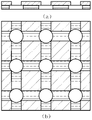
- FIG. 2 is a schematic diagram of a substrate and a copper foil being bonded, and a circular hole is drilled on the top according to an embodiment of the present invention
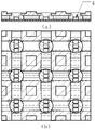
- FIG. 3 is a schematic diagram of an electrode structure formed by a method of machining or etching metal in an embodiment of the present invention
- FIG. 4 is a schematic diagram of forming a stepped electrode structure by a method of half etching or mechanical cutting in an embodiment of the present invention
- FIG. 5 is a schematic diagram of forming a stepped electrode structure by a method of printing metal in an embodiment of the present invention
- FIG. 6 is a schematic diagram of adding a carrier plate under the substrate, placing a chip, and connecting the electrode and the chip through a bonding wire in an embodiment of the present invention
- FIG. 7 is a schematic diagram of injecting low-reflection colloid from above the through hole to completely cover the chip and the bonding wire according to the embodiment of the present invention.
- FIG. 8 is a schematic diagram of cutting the entire board into a single RGB device by cutting in an embodiment of the present invention.
- FIG. 9 is a schematic diagram of welding an RGB device on a circuit board in an embodiment of the present invention.
- FIG. 10 is a schematic diagram showing that the substrate and the copper foil are bonded, and a square hole is drilled thereon in an embodiment of the present invention.
- the azimuth description such as the azimuth or position relationship indicated by up, down, front, rear, left, right, etc.
- the azimuth description is based on the azimuth or position relationship shown in the drawings, only In order to facilitate the description of the present invention and simplify the description, it is not indicated or implied that the indicated device or element must have a particular orientation, be constructed and operated in a particular orientation, and therefore should not be construed as limiting the present invention.
- the meaning of several is one or more, the meaning of multiple is two or more, greater than, less than, exceeding, etc. are understood as not including this number, above, below, within, etc. are understood as including this number. If it is described that the first and the second are only for the purpose of distinguishing technical features, it cannot be understood as indicating or implying relative importance, or indicating the number of the indicated technical features or the order of the indicated technical features. relation.
- this embodiment provides a high-contrast RGB device with a stepped electrode structure, including: a carrier board 1 , the carrier board is provided with a substrate 2 with through holes 6 , and a stepped structure is provided on the substrate.
- the conductive electrode 3 has a built-in RGB chip 4.
- the RGB chip 4 is connected with the step electrode 3 (ie, the conductive electrode) by bonding wires.
- the stepped electrode structure includes an electrode upper surface 3-1 and an electrode lower surface 3-2, wherein the electrode upper surface is used for soldering circuit boards, and the electrode lower surface is used for connecting RGB chips.
- 1(a) is a front view of the RGB device
- FIG. 1(b) is a top view of the RGB device.
- the step electrode structure includes an electrode upper surface 3-1 and an electrode lower surface 3-2, wherein the electrode upper surface is used for soldering circuit boards, the electrode lower surface is used for connecting RGB chips, and the electrode upper surface is used for connecting RGB chips.
- the height between 3-1 and the electrode lower surface 3-2 is 0.05-0.3 mm, and the height between the electrode lower surface 3-2 and the substrate 2 is 0.05-0.5 mm.
- the step electrode 3 structure is formed by mechanical cutting, metal etching, metal printing, or a combination of the three methods.
- the material of the step electrode is one of metals with good electrical conductivity such as silver, copper and aluminum, preferably copper.
- the bonding wire is a metal with good electrical conductivity, such as gold, silver, copper, etc., preferably gold.
- the bonding wires connect the positive or negative electrodes of the three chips (RGB chips include three chips) to the same step electrode, and the other electrodes of the three chips are respectively connected to the other three step electrodes, so as to form a A structure that individually controls the luminous intensity of a single chip.
- the three chips emit different proportions of red, green and blue light through currents of different sizes to adjust the color of the light.
- the RGB chip is cured and fixed by a low-reflection colloid, and the surrounding low-reflection colloid can absorb most of the external light, which can greatly increase the black ratio of the device, thereby improving the contrast of the RGB device.
- the RGB chips are first placed on the carrier board, and the chips and the step electrodes are connected by bonding wires.
- the three chips emit different proportions of red, green and blue light through currents of different sizes to adjust the color of the light.
- the RGB chip is cured and fixed by a low-reflection colloid, and the surrounding low-reflection colloid can absorb most of the external light, which can greatly increase the black ratio of the device, thereby improving the contrast ratio of the RGB device.
- the substrate of the single RGB device has at least one hole, and each hole has at least one group of RGB devices.
- the carrier plate is glass, plastic or film with a transmittance greater than 50% and a thickness of less than 0.3 mm.
- the substrate is an opaque insulating material such as a BT board, an FR4 board or a black epoxy resin doped with carbon particles, preferably a black material.
- the low-reflection colloid filled in the cavity is black colloid or gray colloid, preferably black colloid, and its reflective degree should be lower than 30%.
- the present embodiment provides a preparation method of an RGB device, comprising the following steps:
- FIG. 2( a ) is a cross-sectional view after the copper foil and the substrate are bonded and punched
- FIG. 2( b ) is a top view after the copper foil and the substrate are bonded and punched.
- FIG. 3(a) is a cross-sectional view of the electrode structure and the substrate
- FIG. 3(b) is a top view of the electrode structure and the substrate.
- FIG. 4 is a cross-sectional view of the conductive electrode and the substrate
- FIG. 4( b ) is a top view of the conductive electrode and the substrate.
- FIG. 6(a) is the cross-sectional view of the RGB device without glue injection
- Figure 6(b) is the top view of the RGB device without glue injection
- Figure 7(a) is the cross-sectional view of the RGB device after glue injection
- Figure 7 (b) is the top view of the RGB device after injection.
- FIG. 8(a) is a cross-sectional view of a single RGB device
- FIG. 8(b) is a top view of a single RGB device.
- FIG. 9( a ) is a cross-sectional view of being welded to the circuit board
- FIG. 9( b ) is a top view of being welded to the circuit board.
- This embodiment provides a preparation method of an RGB device, and the preparation steps are the same as those in Embodiment 1, except that:
- step C the method of processing the step electrode is different, and here the step electrode structure is processed by the method of mechanical cutting.
- This embodiment provides a preparation method of an RGB device, and the preparation steps are the same as those in Embodiment 1, except that:
- step C the method of processing the step electrode is different.
- the step electrode structure is processed by the method of printing metal, as shown in FIG. 5 .
- 5( a ) is a cross-sectional view of the conductive electrode and the substrate
- FIG. 5( b ) is a top view of the conductive electrode and the substrate.
- This embodiment provides a preparation method of an RGB device, and the preparation steps are the same as those in Embodiment 1, except that:
- Fig. 10(a) is a cross-sectional view of the RGB device with square holes after injection
- Fig. 10(b) is a top view of the RGB device with square holes after injection.
- This embodiment provides a preparation method of an RGB device, and the preparation steps are the same as those in Embodiment 1, except that:
- the adhesive material used in step D is different, here a debondable material is used, and the carrier plate can be removed by debonding.
- this embodiment provides a high-contrast RGB device with stepped electrodes, which is used to solve the problem of circuit stability when the RGB device is installed on a circuit board.
- the method of half etching, mechanical cutting or printing metal forms the electrode of the step structure, which avoids the direct contact of the bonding wire with the circuit board when the RGB device is installed on the circuit board, and ensures the stability of the circuit structure.
- a removable carrier is glued under the substrate, RGB chips are placed above the carrier, the chips and step electrodes are connected by bonding wires, and low-reflection colloid is injected from above for curing to protect the complete chip and bonding wire structure.
- this structure The contrast ratio of the RGB device can be effectively improved.
- the functions/operations noted in the block diagrams may occur out of the order noted in the operational diagrams.
- two blocks shown in succession may, in fact, be executed substantially concurrently or the blocks may sometimes be executed in the reverse order, depending upon the functionality/operations involved.
- the embodiments presented and described in the flowcharts of the present invention are provided by way of example in order to provide a more comprehensive understanding of the technology. The disclosed methods are not limited to the operations and logic flows presented herein. Alternative embodiments are contemplated in which the order of the various operations are altered and in which sub-operations described as part of larger operations are performed independently.
- the functions, if implemented in the form of software functional units and sold or used as independent products, may be stored in a computer-readable storage medium.
- the technical solution of the present invention can be embodied in the form of a software product in essence, or the part that contributes to the prior art or the part of the technical solution.
- the computer software product is stored in a storage medium, including Several instructions are used to cause a computer device (which may be a personal computer, a server, or a network device, etc.) to execute all or part of the steps of the methods described in the various embodiments of the present invention.
- the aforementioned storage medium includes: U disk, mobile hard disk, Read-Only Memory (ROM, Read-Only Memory), Random Access Memory (RAM, Random Access Memory), magnetic disk or optical disk and other media that can store program codes .
- a "computer-readable medium” can be any device that can contain, store, communicate, propagate, or transport the program for use by or in connection with an instruction execution system, apparatus, or apparatus.
- computer readable media include the following: electrical connections with one or more wiring (electronic devices), portable computer disk cartridges (magnetic devices), random access memory (RAM), Read Only Memory (ROM), Erasable Editable Read Only Memory (EPROM or Flash Memory), Fiber Optic Devices, and Portable Compact Disc Read Only Memory (CDROM).
- the computer readable medium may even be paper or other suitable medium on which the program may be printed, as it may be possible, for example, by optically scanning the paper or other medium, followed by editing, interpretation or other suitable medium as necessary process to obtain the program electronically and then store it in computer memory.
- various parts of the present invention may be implemented in hardware, software, firmware or a combination thereof.
- various steps or methods may be implemented in software or firmware stored in memory and executed by a suitable instruction execution system.
- a suitable instruction execution system For example, if implemented in hardware, as in another embodiment, it can be implemented by any one or a combination of the following techniques known in the art: Discrete logic circuits, application specific integrated circuits with suitable combinational logic gates, Programmable Gate Arrays (PGA), Field Programmable Gate Arrays (FPGA), etc.
Landscapes
- Led Device Packages (AREA)
Abstract
Description
Claims (10)
- 一种具有台阶电极的RGB器件,其特征在于,包括:载板;基板,设置在所述载板上,所述基板上设有通孔;RGB芯片,通过所述通孔设置在所述载板上;导电电极,设置在所述基板上,所述导电电极呈台阶结构,所述导电电极包括电极上表面和电极下表面,所述电极上表面用于焊接线路板,所述电极下表面使用键合线连接所述RGB芯片;低反光胶体,用于覆盖所述RGB芯片和所述键合线。
- 根据权利要求1所述的一种具有台阶电极的RGB器件,其特征在于,所述电极上表面和所述电极下表面之间的高度距离为0.05-0.5mm,所述电极下表面和所述基板之间的高度距离为0.05-0.3mm。
- 根据权利要求1所述的一种具有台阶电极的RGB器件,其特征在于,所述电极下表面在所述载板的投影与所述基板在所述载板的投影部分重叠。
- 根据权利要求1所述的一种具有台阶电极的RGB器件,其特征在于,所述RGB芯片的发光面朝向载板,所述RGB芯片背部的电极面不透光。
- 根据权利要求1所述的一种具有台阶电极的RGB器件,其特征在于,所述低反光胶体的填充高度高于所述电极下表面,且低于所述电极上表面。
- 根据权利要求1所述的一种具有台阶电极的RGB器件,其特征在于,所述通孔的形状为方形或圆形。
- 根据权利要求1所述的一种具有台阶电极的RGB器件,其特征在于,所述导电电极通过机械切割加工、蚀刻金属、印刷金属或者三种方法混合加工而成。
- 根据权利要求1所述的一种具有台阶电极的RGB器件,其特征在于,所述载板为透光度大于50%、厚度小于0.3mm的玻璃、塑料或薄膜;所述基板采用不透光绝缘材料制成,所述基板采用粘接剂与所述载板黏合;所述低反光胶体为黑色胶体或灰色胶体。
- 一种RGB器件的制备方法,其特征在于,包括以下步骤:将铜箔与基板黏合后,在所述铜箔和所述基板上打多个通孔;每个所述通孔上,对所述铜箔进行加工,获得电极结构;对电极结构进行加工,获得具有台阶状的导电电极;在所述基板下方粘合载板,通过所述通孔在所述载板上放置RGB芯片;通过键合线连接所述RGB芯片和所述导电电极;从所述通孔的上方注入低反光胶体固化,覆盖所述RGB芯片和所述键合线;通过切割,获得多个RGB器件。
- 根据权利要求9所述的一种RGB器件的制备方法,其特征在于,所述对电极结构进行加工,获得具有台阶状的导电电极,包括:通过半蚀刻铜箔的方法对电极结构进行加工,获得具有台阶状的导电电极;或者,采用印刷金属的方法对电极结构进行加工,获得具有台阶状的导电电极;或者,通过机械切割加工的方法对电极结构进行加工,获得具有台阶状的导电电极。
Applications Claiming Priority (2)
| Application Number | Priority Date | Filing Date | Title |
|---|---|---|---|
| CN202110142544.1A CN112928105B (zh) | 2021-02-02 | 2021-02-02 | 一种具有台阶电极的rgb器件及制备方法 |
| CN202110142544.1 | 2021-02-02 |
Publications (1)
| Publication Number | Publication Date |
|---|---|
| WO2022166259A1 true WO2022166259A1 (zh) | 2022-08-11 |
Family
ID=76169558
Family Applications (1)
| Application Number | Title | Priority Date | Filing Date |
|---|---|---|---|
| PCT/CN2021/124678 Ceased WO2022166259A1 (zh) | 2021-02-02 | 2021-10-19 | 一种具有台阶电极的rgb器件及制备方法 |
Country Status (2)
| Country | Link |
|---|---|
| CN (1) | CN112928105B (zh) |
| WO (1) | WO2022166259A1 (zh) |
Families Citing this family (4)
| Publication number | Priority date | Publication date | Assignee | Title |
|---|---|---|---|---|
| CN112928105B (zh) * | 2021-02-02 | 2022-10-25 | 华南理工大学 | 一种具有台阶电极的rgb器件及制备方法 |
| CN116612714B (zh) * | 2022-03-27 | 2026-04-10 | 深圳市美矽微半导体股份有限公司 | 一种led载板及其显示设备 |
| CN116170986B (zh) * | 2023-04-25 | 2023-07-18 | 北京理工大学 | 一种灌封系统及方法 |
| CN119451338A (zh) * | 2024-10-31 | 2025-02-14 | 华南理工大学 | 一种具有高环境对比度和高出光效率的led器件 |
Citations (7)
| Publication number | Priority date | Publication date | Assignee | Title |
|---|---|---|---|---|
| CN101060159A (zh) * | 2006-04-21 | 2007-10-24 | 三星电机株式会社 | 具有多阶梯反射表面结构的发光二极管封装及其制造方法 |
| CN202189827U (zh) * | 2011-03-01 | 2012-04-11 | 张栋楠 | 一种led封装模块 |
| CN203631607U (zh) * | 2013-10-10 | 2014-06-04 | 晶科电子(广州)有限公司 | 一种高可靠性led光源及其led模组光源 |
| US20160284678A1 (en) * | 2015-03-23 | 2016-09-29 | Rohm Co., Ltd. | Led package |
| CN208923123U (zh) * | 2018-11-08 | 2019-05-31 | 佛山市国星光电股份有限公司 | 一种led器件和显示屏 |
| CN111162063A (zh) * | 2018-11-08 | 2020-05-15 | 佛山市国星光电股份有限公司 | 一种led器件、显示屏及其封装工艺 |
| CN112928105A (zh) * | 2021-02-02 | 2021-06-08 | 华南理工大学 | 一种具有台阶电极的rgb器件及制备方法 |
Family Cites Families (4)
| Publication number | Priority date | Publication date | Assignee | Title |
|---|---|---|---|---|
| EP1119058A4 (en) * | 1999-07-29 | 2006-08-23 | Citizen Electronics | LIGHT-EMITTING DIODE |
| US6835960B2 (en) * | 2003-03-03 | 2004-12-28 | Opto Tech Corporation | Light emitting diode package structure |
| KR101181112B1 (ko) * | 2005-10-27 | 2012-09-14 | 엘지이노텍 주식회사 | 발광 다이오드, 발광 다이오드 제조 방법 및 발광 다이오드 모듈 |
| CN103490003B (zh) * | 2013-10-10 | 2016-08-31 | 广东晶科电子股份有限公司 | 一种高可靠性led光源及其led模组光源 |
-
2021
- 2021-02-02 CN CN202110142544.1A patent/CN112928105B/zh active Active
- 2021-10-19 WO PCT/CN2021/124678 patent/WO2022166259A1/zh not_active Ceased
Patent Citations (7)
| Publication number | Priority date | Publication date | Assignee | Title |
|---|---|---|---|---|
| CN101060159A (zh) * | 2006-04-21 | 2007-10-24 | 三星电机株式会社 | 具有多阶梯反射表面结构的发光二极管封装及其制造方法 |
| CN202189827U (zh) * | 2011-03-01 | 2012-04-11 | 张栋楠 | 一种led封装模块 |
| CN203631607U (zh) * | 2013-10-10 | 2014-06-04 | 晶科电子(广州)有限公司 | 一种高可靠性led光源及其led模组光源 |
| US20160284678A1 (en) * | 2015-03-23 | 2016-09-29 | Rohm Co., Ltd. | Led package |
| CN208923123U (zh) * | 2018-11-08 | 2019-05-31 | 佛山市国星光电股份有限公司 | 一种led器件和显示屏 |
| CN111162063A (zh) * | 2018-11-08 | 2020-05-15 | 佛山市国星光电股份有限公司 | 一种led器件、显示屏及其封装工艺 |
| CN112928105A (zh) * | 2021-02-02 | 2021-06-08 | 华南理工大学 | 一种具有台阶电极的rgb器件及制备方法 |
Also Published As
| Publication number | Publication date |
|---|---|
| CN112928105B (zh) | 2022-10-25 |
| CN112928105A (zh) | 2021-06-08 |
Similar Documents
| Publication | Publication Date | Title |
|---|---|---|
| WO2022166259A1 (zh) | 一种具有台阶电极的rgb器件及制备方法 | |
| JP4796293B2 (ja) | 照明装置の製造方法 | |
| JP5396215B2 (ja) | 半導体発光装置の製造方法、半導体発光装置および液晶表示装置 | |
| CN107910322A (zh) | 光源组件、显示装置及光源组件的制备方法 | |
| CN104183590B (zh) | 平面光源装置及其导光板的制造方法 | |
| JP2016127253A (ja) | 発光素子のパッケージ構造 | |
| CN102255030B (zh) | 发光模块 | |
| WO2023226611A1 (zh) | 灯板及其制备方法、背光模组 | |
| CN103594463A (zh) | 晶圆倒置式集成led显示封装模块 | |
| CN113745394A (zh) | 发光基板及其制备方法 | |
| CN102064267A (zh) | 显示屏用的led支架单元、led支架及led支架单元的制造方法 | |
| CN109683396A (zh) | 背光模组、显示面板、显示装置及背光模组的制作方法 | |
| JP2008042158A (ja) | Sml型発光ダイオードランプ用素子およびその製造方法 | |
| KR20240003434A (ko) | 발광 기판, 그 제조 방법 및 디스플레이 장치 | |
| CN112802944B (zh) | 一种高对比度的led显示器件及其制造方法和模组 | |
| CN203288590U (zh) | 一种led灯条 | |
| CN106226952A (zh) | 一种背光模组及其制作方法、显示装置 | |
| CN101477954B (zh) | 具高效率侧向发光效果的发光二极管芯片封装方法及结构 | |
| CN210956720U (zh) | 一种led支架、倒装led芯片封装体 | |
| KR100699161B1 (ko) | 발광 소자 패키지 및 그의 제조 방법 | |
| CN206386707U (zh) | Led光源模组 | |
| CN112968019B (zh) | 基板、显示单元、显示模组及其制作方法及显示屏 | |
| JP3238008B2 (ja) | 発光表示装置 | |
| CN104779246A (zh) | 发光组件、背光装置及其制造方法 | |
| CN101465300A (zh) | 发光二极管光条及其制造方法 |
Legal Events
| Date | Code | Title | Description |
|---|---|---|---|
| 121 | Ep: the epo has been informed by wipo that ep was designated in this application |
Ref document number: 21924256 Country of ref document: EP Kind code of ref document: A1 |
|
| NENP | Non-entry into the national phase |
Ref country code: DE |
|
| 122 | Ep: pct application non-entry in european phase |
Ref document number: 21924256 Country of ref document: EP Kind code of ref document: A1 |
|
| 32PN | Ep: public notification in the ep bulletin as address of the adressee cannot be established |
Free format text: NOTING OF LOSS OF RIGHTS PURSUANT TO RULE 112(1) EPC (EPO FORM 1205A DATED 12.02.2024) |
|
| 122 | Ep: pct application non-entry in european phase |
Ref document number: 21924256 Country of ref document: EP Kind code of ref document: A1 |