WO2022157883A1 - プラズマ処理装置 - Google Patents
プラズマ処理装置 Download PDFInfo
- Publication number
- WO2022157883A1 WO2022157883A1 PCT/JP2021/002037 JP2021002037W WO2022157883A1 WO 2022157883 A1 WO2022157883 A1 WO 2022157883A1 JP 2021002037 W JP2021002037 W JP 2021002037W WO 2022157883 A1 WO2022157883 A1 WO 2022157883A1
- Authority
- WO
- WIPO (PCT)
- Prior art keywords
- waveguide
- rectangular waveguide
- plasma
- processing apparatus
- rectangular
- Prior art date
- Legal status (The legal status is an assumption and is not a legal conclusion. Google has not performed a legal analysis and makes no representation as to the accuracy of the status listed.)
- Ceased
Links
Images



Classifications
-
- H—ELECTRICITY
- H01—ELECTRIC ELEMENTS
- H01J—ELECTRIC DISCHARGE TUBES OR DISCHARGE LAMPS
- H01J37/00—Discharge tubes with provision for introducing objects or material to be exposed to the discharge, e.g. for the purpose of examination or processing thereof
- H01J37/32—Gas-filled discharge tubes
- H01J37/32009—Arrangements for generation of plasma specially adapted for examination or treatment of objects, e.g. plasma sources
- H01J37/32192—Microwave generated discharge
- H01J37/32211—Means for coupling power to the plasma
- H01J37/32229—Waveguides
-
- H—ELECTRICITY
- H01—ELECTRIC ELEMENTS
- H01J—ELECTRIC DISCHARGE TUBES OR DISCHARGE LAMPS
- H01J37/00—Discharge tubes with provision for introducing objects or material to be exposed to the discharge, e.g. for the purpose of examination or processing thereof
- H01J37/32—Gas-filled discharge tubes
- H01J37/32009—Arrangements for generation of plasma specially adapted for examination or treatment of objects, e.g. plasma sources
- H01J37/32192—Microwave generated discharge
-
- H—ELECTRICITY
- H01—ELECTRIC ELEMENTS
- H01J—ELECTRIC DISCHARGE TUBES OR DISCHARGE LAMPS
- H01J37/00—Discharge tubes with provision for introducing objects or material to be exposed to the discharge, e.g. for the purpose of examination or processing thereof
- H01J37/32—Gas-filled discharge tubes
- H01J37/32009—Arrangements for generation of plasma specially adapted for examination or treatment of objects, e.g. plasma sources
- H01J37/32192—Microwave generated discharge
- H01J37/32266—Means for controlling power transmitted to the plasma
-
- H—ELECTRICITY
- H01—ELECTRIC ELEMENTS
- H01J—ELECTRIC DISCHARGE TUBES OR DISCHARGE LAMPS
- H01J37/00—Discharge tubes with provision for introducing objects or material to be exposed to the discharge, e.g. for the purpose of examination or processing thereof
- H01J37/32—Gas-filled discharge tubes
- H01J37/32431—Constructional details of the reactor
- H01J37/32458—Vessel
- H01J37/32477—Vessel characterised by the means for protecting vessels or internal parts, e.g. coatings
- H01J37/32495—Means for protecting the vessel against plasma
-
- H—ELECTRICITY
- H05—ELECTRIC TECHNIQUES NOT OTHERWISE PROVIDED FOR
- H05H—PLASMA TECHNIQUE; PRODUCTION OF ACCELERATED ELECTRICALLY-CHARGED PARTICLES OR OF NEUTRONS; PRODUCTION OR ACCELERATION OF NEUTRAL MOLECULAR OR ATOMIC BEAMS
- H05H1/00—Generating plasma; Handling plasma
- H05H1/24—Generating plasma
- H05H1/46—Generating plasma using applied electromagnetic fields, e.g. high frequency or microwave energy
-
- H—ELECTRICITY
- H10—SEMICONDUCTOR DEVICES; ELECTRIC SOLID-STATE DEVICES NOT OTHERWISE PROVIDED FOR
- H10P—GENERIC PROCESSES OR APPARATUS FOR THE MANUFACTURE OR TREATMENT OF DEVICES COVERED BY CLASS H10
- H10P72/00—Handling or holding of wafers, substrates or devices during manufacture or treatment thereof
- H10P72/04—Apparatus for manufacture or treatment
- H10P72/0402—Apparatus for fluid treatment
- H10P72/0418—Apparatus for fluid treatment for etching
- H10P72/0421—Apparatus for fluid treatment for etching for drying etching
-
- H—ELECTRICITY
- H01—ELECTRIC ELEMENTS
- H01J—ELECTRIC DISCHARGE TUBES OR DISCHARGE LAMPS
- H01J2237/00—Discharge tubes exposing object to beam, e.g. for analysis treatment, etching, imaging
- H01J2237/32—Processing objects by plasma generation
- H01J2237/33—Processing objects by plasma generation characterised by the type of processing
- H01J2237/334—Etching
-
- H—ELECTRICITY
- H01—ELECTRIC ELEMENTS
- H01J—ELECTRIC DISCHARGE TUBES OR DISCHARGE LAMPS
- H01J37/00—Discharge tubes with provision for introducing objects or material to be exposed to the discharge, e.g. for the purpose of examination or processing thereof
- H01J37/32—Gas-filled discharge tubes
- H01J37/32009—Arrangements for generation of plasma specially adapted for examination or treatment of objects, e.g. plasma sources
- H01J37/32192—Microwave generated discharge
- H01J37/32311—Circuits specially adapted for controlling the microwave discharge
Definitions
- the present invention relates to a plasma processing apparatus that generates plasma using electromagnetic waves.
- ECR electron cyclotron resonance
- FIG. 1 shows the configuration of an ECR plasma etching processing apparatus 100r according to a comparative example.
- a 2.45 GHz microwave emitted from a magnetron which is a single microwave source, propagates through a rectangular waveguide 14, a circular-rectangular converter 141 and a circular waveguide 142, and an electromagnetic coil 12 is installed outside. It is introduced into the processing chamber 13 through a quartz window 15 in the upper part of the processing chamber 13 where it is located. Electron cyclotron motion is caused by the electric field generated by microwaves and the magnetic field formed perpendicularly thereto.
- the microwave frequency is 2.45 GHz
- electrons perpendicular to the magnetic field are bent by the Lorentz force, so that the electrons gradually move around.
- the operating pressure is around 1 Pa, and a density plasma of 10 11 cm -3 or more can be obtained in this pressure range.
- plasma formation and independent ion energy can be controlled by the RF power source 17 applied to the lower electrode 16, precise shape control is possible.
- a circularly polarized wave is injected into the processing chamber 13 using a circularly polarized wave generator 19 made of a dielectric material.
- a circularly polarized wave is formed also inside the processing chamber 13, and a more uniform plasma distribution can be obtained.
- the plasma density on the wall surface of the processing chamber of a plasma processing apparatus is lower than that in the center of the processing chamber due to the reaction loss on the solid surface.
- the non-uniformity of the plasma density distribution makes the etching rate on the substrate to be processed non-uniform.
- Patent Document 1 in order to improve the non-uniformity of plasma distribution in a processing chamber for large-diameter substrates, a single microwave source is introduced into the processing chamber using a rectangular waveguide branched into two. No countermeasures against annihilation of ions and radicals due to solid surface reactions on the walls of the wall have been taken yet.
- Patent Document 2 in order to improve the etching rate distribution on the processing substrate, two rectangular waveguides are arranged orthogonally and the length of the two orthogonal rectangular waveguides is adjusted.
- the phase of the generated microwave is manipulated to form a circularly polarized wave and then introduced into the processing chamber, it is not possible for the processing chamber to deal with the annihilation of ions and radicals on the wall of the processing chamber, which is a problem of conventional equipment.
- the etching rate of the substrate to be processed does not necessarily depend on the plasma density. Therefore, if priority is given to process conditions such as heat distribution, for example, in order to obtain uniformity, it is necessary to adjust the plasma density in the order of peripheral height, center height, and uniformity within one process cycle. Etching in-plane uniformity on the substrate can be obtained.
- the film thickness formed on the substrate to be processed may become uneven due to characteristics such as the exhaust conductance of the film forming apparatus and the symmetry of the processing chamber.
- the film thickness has a convex distribution such as from high at the center to low at the periphery, a large amount of microwave power is required to be applied to the center of the substrate to be processed.
- the film thickness has a concave distribution such as from low at the center to high at the periphery, it is necessary to reduce the microwave input power on the center of the substrate to be processed.
- an etching apparatus using plasma is required to control plasma density distribution with a high degree of freedom.
- a circularly polarized wave generator 19 made of a dielectric block is provided inside the apparatus 100r.
- the circularly polarized wave generator 19 is covered with the electromagnetic coil 12, there is a problem that it is difficult to adjust its position.
- a plasma processing apparatus includes a processing chamber in which a sample is plasma-processed, a high-frequency power source that supplies microwave high-frequency power for generating plasma, a rectangular waveguide that transmits microwaves, A plasma processing apparatus comprising a circular waveguide connected to the rectangular waveguide for transmitting microwaves to a processing chamber, and a sample stage on which a sample is placed, wherein the rectangular waveguide is vertically partitioned It comprises an upper rectangular waveguide and a lower rectangular waveguide formed, and a cutoff section in which a dielectric is arranged to cut off high frequency power of microwaves supplied from a high frequency power supply.
- the circular waveguide comprises an inner waveguide connected to the upper rectangular waveguide and formed therein, and an outer waveguide connected to the lower rectangular waveguide and formed outside the inner waveguide. do.
- the width of the blocking portion is narrower than the width of the rectangular waveguide other than the blocking portion.
- non-uniformity of the plasma distribution in the processing chamber can be reduced, and the plasma distribution in the processing chamber can be adjusted to medium-high, peripheral high, or flat distribution in accordance with a desired etching process.
- FIG. 1 is a schematic longitudinal sectional view of an ECR plasma etching processing apparatus according to a comparative example.
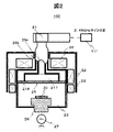
- FIG. 2 is a schematic longitudinal sectional view showing the overall construction of an ECR plasma etching processing apparatus according to the present invention.
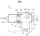
- FIG. 3 is a top view of a waveguide configuration for adjusting microwave power of the present invention.
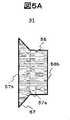
- FIG. 4 is a cross-sectional view of the waveguide configuration along line AA of FIG. 5A is a top view illustrating the outline of the power gate of FIG. 3.
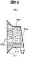
- FIG. FIG. 5B is a top view explaining the outline of the power gate according to the modification.
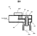
- FIG. 6 is a structural schematic diagram of the power gate driving mechanism of the present invention.
- FIG. 7 is a diagram showing simulation results of the finite element method (HFSS) of the present invention.
- HFSS finite element method
- FIG. 2 is a schematic vertical cross-sectional view showing the overall configuration of the ECR plasma etching apparatus according to the present invention.
- FIG. 3 is a top view of a waveguide configuration for adjusting microwave power of the present invention.
- FIG. 4 is a cross-sectional view of the waveguide configuration along line AA of FIG.
- FIG. 5A shows a top view of the power gate of FIG.
- FIG. 5B is a top view of a modified power gate.
- the microwave plasma etching apparatus 100 supplies microwave power of 2.45 GHz from a single microwave source (high frequency power supply) 101, a magnetron, to the upper part of the processing chamber 23. It has a microwave power splitter 21 that introduces microwaves to a circular inner waveguide 29a and a circular outer waveguide 29b, respectively.
- the circular inner waveguide 29a and the circular outer waveguide 29b can be referred to as circular waveguides.
- the inner waveguide 29a is connected to the inner radiating portion 217.
- the outer waveguide 29b is connected to the ring-shaped outer radiating section 218.
- a magnetron which is a microwave source (high frequency power source) 101, supplies microwave high frequency power for generating plasma.
- a quartz window 25 is provided between the processing chamber 23 and the secondary radiation sections 217 and 218 .
- the outer circumference of the processing chamber 23 is covered with an electromagnetic coil 22 .
- a lower electrode 26 serving as a sample table for placing a substrate (sample) 20 to be processed such as a semiconductor wafer is provided on the central bottom surface of the processing chamber 23 .
- Lower electrode 26 is connected to RF power source 27 for accelerating ions in the plasma. Ions of the processing gas ionized in the plasma are accelerated toward the substrate 20 to be processed by the voltage fluctuation of the RF power source 27, and the thin film on the substrate 20 to be processed can be removed.
- Circularly polarized waves are introduced into the inner waveguide 29a and the outer waveguide 29b by the microwave power splitter 21, respectively, and pass through the inner radiating section 217 and the ring-shaped outer radiating section 218 to the processing chamber 23.
- the microwave power is turned on.
- the TEM mode is mixed at the output end of the outer waveguide 29b (coaxial portion), and the axial ratio of the circularly polarized wave is reduced at the radiation end of the outer waveguide 29b. This effect is used to remove mixed TEM mode microwaves. Therefore, since the TEM mode of the outer waveguide 29b can be removed by the ring-shaped outer radiation portion 218, the axial ratio of the outer waveguide 29b is evaluated using the TE11 mode S parameter.
- the inner radiating portion 217 shown here is a cylindrical space, but it may be a rectangular parallelepiped, a polygon such as a hexahedron or an octahedron, and any shape that allows a higher mode than the TE11 mode to stand.
- FIG. 3 A top view of the microwave power splitter 21 of FIG. 2 is shown in FIG.
- the microwave power splitter 21 consists of a long rectangular waveguide a (first rectangular waveguide) 33 and a short rectangular waveguide perpendicular to (or crossing) the long rectangular waveguide a (or first rectangular waveguide) 33 in top or plan view. and a wave tube b (second rectangular waveguide) 34 .
- Both the rectangular waveguide a33 and the rectangular waveguide b34 can be constructed using an EIAJ standard WRI-22 waveguide (width 109.2 mm, height 54.6 mm).
- FIG. 4 shows a cross-sectional view along line AA in FIG. As shown in FIG.
- the rectangular waveguide a 33 and the rectangular waveguide b 34 are divided into an upper rectangular waveguide 42 and a lower rectangular waveguide 43 by a partition plate 49 in a cross-sectional view. That is, the microwave power splitter 21 consists of rectangular waveguides (33, 34) connected to a single microwave source 101 and circular waveguides (29a) connected to the rectangular waveguides (33, 34). , 29b) and radiating portions (217, 218) connected between the circular waveguides (29a, 29b) and the processing chamber 23.
- the microwave power from the magnetron 101 is split by the partition plate 49 into the upper rectangular waveguide 42 and the lower rectangular waveguide 43 .
- a pair of trapezoidal constrictions 30 are provided on the side walls of the upper rectangular waveguide 42 so as to face each other in order to cut off the power passing through the upper rectangular waveguide 42 .
- the pair of constricted portions 30 can be said to be blocking portions for blocking power passing through the upper rectangular waveguide 42 .
- the width between the pair of constricted portions 30, which are blocking portions, is configured to be narrower than the width of the rectangular waveguide (33) other than the pair of constricted portions 30 in plan view or top view.
- the microwaves blocked by the constricted portions 30 of the upper rectangular waveguide 42 can pass.
- the microwave power entering the circular inner waveguide 29a from the upper rectangular waveguide 42 can be adjusted.
- the constricted portion 30 is basically characterized by oblique sides 301 and 302 on both sides being asymmetrical. As a result, reflection to the microwave source 101 can be reduced, and circularly polarized waves are synthesized by the orthogonal rectangular waveguide a33 and rectangular waveguide b34, so that the impedance can be smoothly changed. .
- a cylindrical dielectric waveguide 36 is formed between an upper rectangular waveguide 42 and an inner waveguide, as shown in FIGS. It is provided between the tubes 29a.
- a dielectric waveguide 36 is arranged in an upper rectangular waveguide 42 .
- the dielectric waveguide 36 can be made of quartz glass.
- the central axis of the dielectric waveguide 36 is configured such that the central axis of the rectangular waveguide a33 and the central axis of the rectangular waveguide b34 do not match (shifted configuration). As shown in FIG.
- a gap 47 of constant distance is provided for adjusting the reactance.
- the TE11 mode is Circularly polarized waves can be synthesized.
- ⁇ d is 2.45 GHz and 148 mm for a WRI-22 standard rectangular waveguide.
- the length L1 indicates the length between the center axis of the dielectric waveguide 36 and the first side wall 34a of the rectangular waveguide b34.
- the length L2 indicates the length between the center axis of the dielectric waveguide 36 and the second side wall 34b facing the first side wall 34a of the rectangular waveguide b34.
- a length L3 indicates the length between the central axis of the dielectric waveguide 36 and the first side wall 33a of the rectangular waveguide a33.
- a length L4 indicates the length between the center axis of the dielectric waveguide 36 and the end portion 33b of the rectangular waveguide a33 facing the first side wall 33a.
- the length of the short rectangular waveguide b34 (L1+L2) ⁇ the length of the long rectangular waveguide a33 (L3+L4).
- the first side wall 34a and the second side wall 34b of the rectangular waveguide b34 are a pair of side walls in the longitudinal direction of the rectangular waveguide b34. Longitudinal sidewalls and ends of tube a33.
- the microwave power passing through the upper rectangular waveguide 42 can be adjusted by the length 700 of inserting the power gate 31 into the constricted portion 30 of the upper rectangular waveguide 42 . Furthermore, circularly polarized waves are synthesized by the crossing portion 35 of the rectangular waveguides a 33 and the rectangular waveguides b 34 arranged orthogonally, and the circularly polarized microwaves having different power ratios inside and outside the processing chamber 23 are generated. You can throw in waves.
- the plasma density distribution in the processing chamber 23 can be continuously controlled to have a central height, a peripheral height, and a flat distribution depending on the different internal and external power ratios of the microwaves.
- the power gate 31 has a trapezoidal trapezoidal portion 57 including an upper base 57a and a lower base 57b, and a rectangular insert 58 connected to the upper base 57a of the trapezoidal portion 57. As shown in FIG. .
- the insert portion 58 is configured to be inserted into the constricted portion 30 of the upper rectangular waveguide 42 .
- the trapezoidal portion 57 has an end face 58b that is horizontal or parallel to the upper base 57a or the lower base 57b.
- the power gate 31a includes a trapezoidal trapezoidal portion 57 including an upper base 57a and a lower base 57b, and an insertion portion 58a connected to the upper base 57a of the trapezoidal portion 57.
- the insert portion 58a has an end surface 58c that has a constant angle 59 with respect to the upper base 57a or the lower base 57b of the trapezoidal portion 57.
- the end face 58c has the effect of reducing the reflection of microwaves to the microwave source 101.
- FIG. 7 is a diagram showing simulation results of the finite element method (HFSS) of the present invention.
- FIG. 7 shows the finite element method simulation results when the microwave power divider 21 receives 2.45 GHz microwaves from the microwave source 101 and the insertion length 700 of the power gate 31 is varied.
- FIG. 7 shows a graph 71 showing changes in the axial ratio of circularly polarized waves radiated from the inner waveguide 29a, a graph 72 showing the axial ratio of circularly polarized waves radiated from the outer waveguide 29b, and a microwave source 101. and a graph 74 showing the internal/external power ratio of the inner waveguide 29a and the outer waveguide 29b.
- the inside/outside power ratio can be controlled within a linear range of 0.18 to 0.078, and the axial ratio between the inner waveguide 29a and the outer waveguide 29b should be 0.9 or more. It was confirmed that the reflection was 0.2 or less while maintaining the reflection.
- the ECR plasma etching apparatus 100 of the present invention has the following configuration.
- the microwave power splitter 21 has the function of a circularly polarized wave generator, and the waveguide configuration for forming circularly polarized waves by the circularly polarized wave generator 19 of the comparative example is ECR plasma etched. It is mounted outside the device 100 as a waveguide for the microwave introduction portion of the device 100 . This makes it possible to flexibly cope with changes in the plasma density distribution in the processing chamber 23 due to process conditions.
- the microwave power splitter 21 consists of a long rectangular waveguide 33 connected to a single microwave source 101, the magnetron, and a short rectangular waveguide 33 orthogonal (or crossed) with the long rectangular waveguide 33. It is configured using a tube 34 .
- a circularly polarized wave is formed inside each of the connected inner waveguide 29a and outer waveguide 29b.
- the rectangular waveguides 33 and 34 arranged orthogonally are provided with a partition plate 49 to vertically divide the rectangular waveguides 33 and 34 so that the power of the single microwave source 101 can be divided into two.
- the rectangular waveguide divided vertically by the partition plate 49 has an upper rectangular waveguide 42 and a lower rectangular waveguide 43 . Also, by changing the height of the partition plate 49, the microwave power ratio divided into two can be adjusted.
- An upper rectangular waveguide 42 and a lower rectangular waveguide 43 vertically divided by a partition plate 49 form a double waveguide structure connected to a circular inner waveguide 29a and a circular outer waveguide 29b, respectively. Due to the increased diameter of this dual waveguide structure, a cylindrical dielectric waveguide 36, e.g. By loading the waveguide 36, there is an advantage that the wavelength of the microwave can be compressed and the diameter of the double waveguide portion can be designed small. Further, by slightly shifting the central axis of the dielectric waveguide 36 as the quartz waveguide from the central axis of the rectangular waveguides 33 and 34, it is possible to reduce the reflection to the microwave source 101. Circularly polarized waves can also be formed in the circular outer waveguide 29b.
- designing the radius a of the inner waveguide 29a according to formula (1) allows the microwaves to pass through or be blocked.
- a (1.841C)/(2 ⁇ fc)[m] (1)
- fc is the microwave frequency of 2.45 GHz and C is the speed of light in vacuum of 2.99 ⁇ 10 8 m/s.
- the radius of the inner waveguide 29a is 0.0375 m.
- the material of the dielectric waveguide 36 in the inner waveguide 29a is quartz and its relative dielectric constant ⁇ r is 3.78, the propagation speed of the microwave is reduced to 1/ ⁇ r, so the equation According to (1), the radius of the inner waveguide 29a is 0.018 m.
- the outer waveguide 29b is configured to be coaxial with the inner waveguide 29a. Also, the central axis of the dielectric waveguide 36 is configured to be coaxial with the outer waveguide 29b and the inner waveguide 29a. Therefore, the outer waveguide 29b propagates microwaves as a coaxial waveguide with the inner waveguide 29a.
- the TEM mode which is the fundamental mode
- the radius b of the outer waveguide 29b when the higher-order mode, TE11, is shielded can be determined using the following equation (2). can be done.
- kc is the cutoff wave number [rad/m]
- a is the radius [m] of the inner waveguide 29a
- b is the radius [m] of the outer waveguide 29b.
- circularly polarized waves are supplied to the inner waveguide 29a and the outer waveguide 29b, which are double waveguides formed by the partition plate 49, respectively. can be formed. Since the outer waveguide 29b is a coaxial waveguide, the lowest order mode is the TEM mode.
- the parameters were used to evaluate the axial ratios of the circularly polarized waves formed by the inner waveguide 29a and the outer waveguide 29b, respectively (see graphs 71 and 72 in FIG. 7).
- a circularly polarized wave with an axial ratio of 1 indicates perfect circular polarization, and an axial ratio of 0 indicates a linearly polarized wave.
- Microwave in upper rectangular waveguide 42 connected to inner waveguide 29a to adjust microwave power radiated from inner waveguide (circular portion) 29a and outer waveguide (coaxial portion) 29b.
- a pair of constrictions 30 capable of blocking microwaves are provided in the incident wave direction.
- the width of the upper rectangular waveguide 42 is narrowed by the pair of constricted portions 30, the microwave from the microwave source 101 is cut off, and power cannot be transmitted.
- a slidable quartz block (power gate) 31 is provided. By moving the power gate 31 back and forth, the microwave power passing through the upper rectangular waveguide 42 can be adjusted.
- the power of the inner waveguide 29a is introduced into the processing chamber 23 from the inner radiation section 217, while the power of the outer waveguide 29b is once introduced into a cavity such as the ring-shaped outer radiation section 218 and then radiated into the processing chamber 23. be.
- the outer waveguide 29b is a coaxial waveguide, its lowest order mode is the TEM mode. Therefore, the TEM mode is mixed at the output end of the outer waveguide (coaxial portion) 29b, and the axial ratio of the circularly polarized wave is reduced at the radiation end of the outer waveguide 29b.
- the cavity resonance effect is used to remove the mixed TEM mode microwaves. Therefore, since the TEM mode of the outer waveguide 29b can be removed by the ring-shaped outer radiation portion 218, the axial ratio of the outer waveguide 29b is evaluated using the TE11 mode S parameter.
- this inner radiation part 217 by making the space larger in diameter than the inner waveguide 29a, this inner radiation part 217 can also raise modes other than TE11. Since this electric field can be rotated in time, the influence of the wave reflected as the TE11 mode can be reduced.
- the example of the inner radiating portion 217 shown here is a cylindrical space, but it may be a rectangular parallelepiped, a polygon such as a hexahedron or an octahedron, and any shape that allows a higher mode than the TE11 mode to stand.
- the microwave power is divided into two when introduced into the processing chamber 23 , and the power of the inner waveguide 29 a is controlled by the insertion length 700 of the power gate 31 . Therefore, during the semiconductor device etching process, the insertion length 700 of the power gate 31 can be adjusted to match the plasma distribution in the processing chamber 23 to the desired etching rate. Therefore, the non-uniformity of the plasma distribution in the processing chamber 23 of the plasma processing apparatus 100 is reduced, and the plasma density distribution in the processing chamber 23 is adjusted to center high, peripheral high, or flat distribution according to a desired etching process. becomes possible.
- the power gate 31 of Example 1 shown in FIGS. 3 and 4 is a configuration example made of silica glass in accordance with the microwave source 101 of 2.45 GHz.
- the material and shape of power gate 31 may be changed to match the frequency.
- alumina, MC nylon resin, fluorine resin, or the like may be used.
- the power gate 31 and the constricted portion 30 are provided in the upper rectangular waveguide 42 in the first embodiment, the example configuration has been described, but the present invention is not limited to this.
- the power gate 31 and constriction 30 can be provided only in the lower rectangular waveguide 43, not in the upper rectangular waveguide 42.
- a gap 47 shown in FIG. 4 is provided to adjust the axial ratio of the circularly polarized wave by the power of the reflected wave according to the plasma density in the processing chamber 23 .
- the interval or size of the gap 47 can be adjusted.
- the impedance changes due to the plasma density in the processing chamber 23 in FIG. Axial ratio of waves may be reduced. Therefore, metal or dielectric cylinders or projections with a diameter of 3 to 5 mm and a length of 5 to 18 mm are installed at appropriate locations on the upper and lower rectangular waveguides 42 and 43 at one or more locations. By matching the impedance, the axial ratio of the circularly polarized waves of the upper rectangular waveguide 42 and the lower rectangular waveguide 43 can be finely adjusted.
- FIG. 6 is a schematic diagram of the configuration of the power gate driving mechanism of the present invention.
- Power gate 31 is preferably slidably positioned within upper rectangular waveguide 42, i.e., between waist 30 of FIG. Therefore, as shown in FIG. 6, it is preferable to provide an actuator 627 as a moving mechanism for sliding the power gate 31 between the constricted portions 30 .
- Actuator 627 is connected to a process control PC (personal computer, not shown) or WS (work station, not shown) and configured to move power gate 31 between waist 30 .
- PC personal computer, not shown
- WS work station, not shown
- a plasma processing apparatus (100) includes a processing chamber (23) in which a sample (20) is plasma-processed, a high-frequency power source (101) for supplying high-frequency power of microwaves for generating plasma, and , circular waveguides (29a, 29b) connected to the rectangular waveguides and transmitting microwaves to the processing chamber, and a sample on which the sample is placed a base (26).
- the rectangular waveguides (33, 34) are composed of an upper rectangular waveguide (42) and a lower rectangular waveguide (43) which are vertically partitioned, and a microwave high frequency wave supplied from the high frequency power supply.
- Said circular waveguides (29a, 29b) are connected to said upper rectangular waveguide (42) and internally formed inner waveguide (29a) and said lower rectangular waveguide (43). and an outer waveguide (29b) formed outside the inner waveguide.
- the width of the blocking portion (30) is narrower than the width of the rectangular waveguide (33) other than the blocking portion (30).
- the rectangular waveguides (33, 34) include a first rectangular waveguide (33) and a second rectangular waveguide ( 34) and
- the inner waveguide (29a) has a dielectric waveguide (36).
- the central axis of the dielectric waveguide (36) in the plan view is the same as the central axis of the first rectangular waveguide (33) in the plan view and the second rectangular waveguide It does not coincide with the central axis of (34).
- the dielectric (31) is arranged in the upper rectangular waveguide.
- the dielectric (31) is arranged in the upper rectangular waveguide.
- a moving mechanism (627) for moving the dielectric (31) is further provided.
- Microwave power divider 22 Electromagnetic coil 23: Processing chamber 25: Quartz window 26: Lower electrode 27: RF power supply 101: Magnetron (microwave source, high frequency power supply) 217: inner radiating portion 218: ring-shaped outer radiating portion 29a: circular inner waveguide 29b: circular outer waveguide 30: constricted portion 31: quartz gate (power gate) 33: Rectangular waveguide a 34: Rectangular waveguide b 36: Dielectric waveguide 42: Upper rectangular waveguide 43: Lower rectangular waveguide 47: Gap 49: Partition plate 57: Trapezoidal portion 58: Insertion portion 627: Actuator (moving mechanism) 700: insertion length
Landscapes
- Physics & Mathematics (AREA)
- Engineering & Computer Science (AREA)
- Plasma & Fusion (AREA)
- Chemical & Material Sciences (AREA)
- Analytical Chemistry (AREA)
- Electromagnetism (AREA)
- Spectroscopy & Molecular Physics (AREA)
- Plasma Technology (AREA)
- Drying Of Semiconductors (AREA)
- Encapsulation Of And Coatings For Semiconductor Or Solid State Devices (AREA)
Abstract
Description
ここで、fcはマイクロ波周波数2.45GHz、Cは真空中光速度2.99×10⁸m/sである。
ここで、kcは遮断波数[rad/m]、aは内側導波管29aの半径[m]、bは外側導波管29bの半径[m]である。
前記矩形導波管(33,34)は、上下に仕切られて形成された上部矩形導波管(42)および下部矩形導波管(43)と、前記高周波電源から供給されたマイクロ波の高周波電力を遮断し誘電体(31)が配置された遮断部(30)とを具備する。
前記円形導波管(29a、29b)は、前記上部矩形導波管(42)に接続され内部に形成された内側導波管(29a)と、前記下部矩形導波管(43)に接続され前記内側導波管の外側に形成された外側導波管(29b)とを具備する。
前記遮断部(30)の幅は、前記遮断部(30)以外の前記矩形導波管(33)の幅より狭い。
21:マイクロ波電力分割器
22:電磁コイル
23:処理室
25:石英窓
26:下部電極
27:RF電源
101:マグネトロン(マイクロ波源、高周波電源)
217:内側放射部
218:リング状外側放射部
29a:円形内側導波管
29b:円形外側導波管
30:くびれ部
31:石英ゲート(電力ゲート)
33:矩形導波管a
34:矩形導波管b
36:誘電体導波路
42:上部矩形導波管
43:下部矩形導波管
47:隙間
49:仕切板
57:台形部
58:挿入部
627:アクチュエータ(移動機構)
700:挿入長
Claims (7)
- 試料がプラズマ処理される処理室と、プラズマを生成するためのマイクロ波の高周波電力を供給する高周波電源と、前記マイクロ波を伝送する矩形導波管と、前記矩形導波管に接続され前記処理室へマイクロ波を伝送する円形導波管と、前記試料が載置される試料台とを備えるプラズマ処理装置において、
前記矩形導波管は、上下に仕切られて形成された上部矩形導波管および下部矩形導波管と、前記高周波電源から供給されたマイクロ波の高周波電力を遮断し誘電体が配置された遮断部とを具備し、
前記円形導波管は、前記上部矩形導波管に接続され内部に形成された内側導波管と、前記下部矩形導波管に接続され前記内側導波管の外側に形成された外側導波管とを具備し、
前記遮断部の幅は、前記遮断部以外の前記矩形導波管の幅より狭いことを特徴とするプラズマ処理装置。 - 請求項1に記載のプラズマ処理装置において、
前記矩形導波管は、第1の矩形導波管と、前記第1の矩形導波管と直交する第2の矩形導波管と、を具備することを特徴とするプラズマ処理装置。 - 請求項2に記載のプラズマ処理装置において、
前記内側導波管は、誘電体導波路を有することを特徴とするプラズマ処理装置。 - 請求項3に記載のプラズマ処理装置において、
平面図における前記誘電体導波路の中心軸は、前記平面図における前記第1の矩形導波管の中心軸および前記第2の矩形導波管の中心軸と一致しないことを特徴とするプラズマ処理装置。 - 請求項1に記載のプラズマ処理装置において、
前記誘電体は、前記上部矩形導波管に配置されていることを特徴とするプラズマ処理装置。 - 請求項3に記載のプラズマ処理装置において、
前記誘電体は、前記上部矩形導波管に配置されていることを特徴とするプラズマ処理装置。 - 請求項1に記載のプラズマ処理装置において、
前記誘電体を移動させる移動機構をさらに備えることを特徴とするプラズマ処理装置。
Priority Applications (6)
| Application Number | Priority Date | Filing Date | Title |
|---|---|---|---|
| US17/641,503 US11948776B2 (en) | 2021-01-21 | 2021-01-21 | Plasma processing apparatus |
| PCT/JP2021/002037 WO2022157883A1 (ja) | 2021-01-21 | 2021-01-21 | プラズマ処理装置 |
| CN202180004749.1A CN115119543B (zh) | 2021-01-21 | 2021-01-21 | 等离子处理装置 |
| JP2022506208A JP7302094B2 (ja) | 2021-01-21 | 2021-01-21 | プラズマ処理装置 |
| KR1020227003176A KR102837446B1 (ko) | 2021-01-21 | 2021-01-21 | 플라스마 처리 장치 |
| TW111101288A TWI808609B (zh) | 2021-01-21 | 2022-01-12 | 電漿處理裝置 |
Applications Claiming Priority (1)
| Application Number | Priority Date | Filing Date | Title |
|---|---|---|---|
| PCT/JP2021/002037 WO2022157883A1 (ja) | 2021-01-21 | 2021-01-21 | プラズマ処理装置 |
Publications (1)
| Publication Number | Publication Date |
|---|---|
| WO2022157883A1 true WO2022157883A1 (ja) | 2022-07-28 |
Family
ID=82548603
Family Applications (1)
| Application Number | Title | Priority Date | Filing Date |
|---|---|---|---|
| PCT/JP2021/002037 Ceased WO2022157883A1 (ja) | 2021-01-21 | 2021-01-21 | プラズマ処理装置 |
Country Status (6)
| Country | Link |
|---|---|
| US (1) | US11948776B2 (ja) |
| JP (1) | JP7302094B2 (ja) |
| KR (1) | KR102837446B1 (ja) |
| CN (1) | CN115119543B (ja) |
| TW (1) | TWI808609B (ja) |
| WO (1) | WO2022157883A1 (ja) |
Cited By (1)
| Publication number | Priority date | Publication date | Assignee | Title |
|---|---|---|---|---|
| TWI899592B (zh) * | 2022-10-19 | 2025-10-01 | 日商日立全球先端科技股份有限公司 | 電漿處理裝置 |
Families Citing this family (3)
| Publication number | Priority date | Publication date | Assignee | Title |
|---|---|---|---|---|
| JP2024147876A (ja) * | 2023-04-04 | 2024-10-17 | 東京エレクトロン株式会社 | プラズマ処理装置 |
| TW202514705A (zh) | 2023-05-30 | 2025-04-01 | 荷蘭商Asm Ip私人控股有限公司 | 用於將能量提供至具有多個功率信號輸入之電漿腔室的系統以及半導體處理系統 |
| CN119255465B (zh) * | 2024-09-25 | 2025-08-12 | 成都理工大学 | 一种基于电子回旋共振的等离子体炬及其简化仿真方法 |
Citations (5)
| Publication number | Priority date | Publication date | Assignee | Title |
|---|---|---|---|---|
| JPH01134926A (ja) * | 1987-11-20 | 1989-05-26 | Nippon Telegr & Teleph Corp <Ntt> | プラズマ生成源およびそれを用いたプラズマ処理装置 |
| JP2005050776A (ja) * | 2003-07-31 | 2005-02-24 | Tokyo Electron Ltd | 電磁界供給装置およびプラズマ装置 |
| JP2012178380A (ja) * | 2011-02-25 | 2012-09-13 | Hitachi High-Technologies Corp | プラズマ処理装置 |
| WO2016104205A1 (ja) * | 2014-12-26 | 2016-06-30 | 東京エレクトロン株式会社 | プラズマ処理装置及びプラズマ処理方法 |
| JP2019110028A (ja) * | 2017-12-18 | 2019-07-04 | 株式会社日立ハイテクノロジーズ | プラズマ処理装置 |
Family Cites Families (18)
| Publication number | Priority date | Publication date | Assignee | Title |
|---|---|---|---|---|
| US5024716A (en) * | 1988-01-20 | 1991-06-18 | Canon Kabushiki Kaisha | Plasma processing apparatus for etching, ashing and film-formation |
| JPH0878190A (ja) * | 1994-09-01 | 1996-03-22 | Kokusai Electric Co Ltd | マイクロ波放電装置及び放電方法 |
| JP3310957B2 (ja) * | 1999-08-31 | 2002-08-05 | 東京エレクトロン株式会社 | プラズマ処理装置 |
| JP4593741B2 (ja) * | 2000-08-02 | 2010-12-08 | 東京エレクトロン株式会社 | ラジアルアンテナ及びそれを用いたプラズマ処理装置 |
| JP3390918B2 (ja) | 2000-10-10 | 2003-03-31 | 日立マクセル株式会社 | 磁気記録媒体 |
| JP2002299240A (ja) * | 2001-03-28 | 2002-10-11 | Tadahiro Omi | プラズマ処理装置 |
| JP5213150B2 (ja) * | 2005-08-12 | 2013-06-19 | 国立大学法人東北大学 | プラズマ処理装置及びプラズマ処理装置を用いた製品の製造方法 |
| WO2011021607A1 (ja) * | 2009-08-21 | 2011-02-24 | 東京エレクトロン株式会社 | プラズマ処理装置および基板処理方法 |
| US20120186747A1 (en) | 2011-01-26 | 2012-07-26 | Obama Shinji | Plasma processing apparatus |
| JP2012190899A (ja) * | 2011-03-09 | 2012-10-04 | Hitachi High-Technologies Corp | プラズマ処理装置 |
| JP2015109249A (ja) * | 2013-10-22 | 2015-06-11 | 東京エレクトロン株式会社 | プラズマ処理装置 |
| JP6442242B2 (ja) * | 2014-11-17 | 2018-12-19 | 株式会社日立ハイテクノロジーズ | プラズマ処理装置 |
| JP6560071B2 (ja) * | 2015-09-11 | 2019-08-14 | 株式会社日立ハイテクノロジーズ | プラズマ処理装置 |
| JP6552429B2 (ja) * | 2016-02-05 | 2019-07-31 | 東京エレクトロン株式会社 | プラズマ処理装置 |
| JP6695705B2 (ja) * | 2016-02-17 | 2020-05-20 | 東京エレクトロン株式会社 | プラズマ処理装置 |
| JP6752117B2 (ja) * | 2016-11-09 | 2020-09-09 | 東京エレクトロン株式会社 | マイクロ波プラズマ源およびマイクロ波プラズマ処理装置 |
| CN113454760B (zh) * | 2020-01-27 | 2024-03-22 | 株式会社日立高新技术 | 等离子处理装置 |
| WO2021220459A1 (ja) * | 2020-04-30 | 2021-11-04 | 株式会社日立ハイテク | プラズマ処理装置 |
-
2021
- 2021-01-21 JP JP2022506208A patent/JP7302094B2/ja active Active
- 2021-01-21 WO PCT/JP2021/002037 patent/WO2022157883A1/ja not_active Ceased
- 2021-01-21 KR KR1020227003176A patent/KR102837446B1/ko active Active
- 2021-01-21 US US17/641,503 patent/US11948776B2/en active Active
- 2021-01-21 CN CN202180004749.1A patent/CN115119543B/zh active Active
-
2022
- 2022-01-12 TW TW111101288A patent/TWI808609B/zh active
Patent Citations (5)
| Publication number | Priority date | Publication date | Assignee | Title |
|---|---|---|---|---|
| JPH01134926A (ja) * | 1987-11-20 | 1989-05-26 | Nippon Telegr & Teleph Corp <Ntt> | プラズマ生成源およびそれを用いたプラズマ処理装置 |
| JP2005050776A (ja) * | 2003-07-31 | 2005-02-24 | Tokyo Electron Ltd | 電磁界供給装置およびプラズマ装置 |
| JP2012178380A (ja) * | 2011-02-25 | 2012-09-13 | Hitachi High-Technologies Corp | プラズマ処理装置 |
| WO2016104205A1 (ja) * | 2014-12-26 | 2016-06-30 | 東京エレクトロン株式会社 | プラズマ処理装置及びプラズマ処理方法 |
| JP2019110028A (ja) * | 2017-12-18 | 2019-07-04 | 株式会社日立ハイテクノロジーズ | プラズマ処理装置 |
Cited By (1)
| Publication number | Priority date | Publication date | Assignee | Title |
|---|---|---|---|---|
| TWI899592B (zh) * | 2022-10-19 | 2025-10-01 | 日商日立全球先端科技股份有限公司 | 電漿處理裝置 |
Also Published As
| Publication number | Publication date |
|---|---|
| JP7302094B2 (ja) | 2023-07-03 |
| CN115119543B (zh) | 2025-10-14 |
| KR20220107148A (ko) | 2022-08-02 |
| CN115119543A (zh) | 2022-09-27 |
| US11948776B2 (en) | 2024-04-02 |
| TW202231134A (zh) | 2022-08-01 |
| JPWO2022157883A1 (ja) | 2022-07-28 |
| US20230352273A1 (en) | 2023-11-02 |
| KR102837446B1 (ko) | 2025-07-25 |
| TWI808609B (zh) | 2023-07-11 |
Similar Documents
| Publication | Publication Date | Title |
|---|---|---|
| JP7302094B2 (ja) | プラズマ処理装置 | |
| JP7139528B2 (ja) | プラズマ処理装置 | |
| KR100472582B1 (ko) | 플라즈마처리장치 | |
| CN102027575B (zh) | 微波导入机构、微波等离子源以及微波等离子处理装置 | |
| US8945342B2 (en) | Surface wave plasma generating antenna and surface wave plasma processing apparatus | |
| US5173641A (en) | Plasma generating apparatus | |
| KR19980024951A (ko) | 마이크로파 플라즈마 처리 장치 | |
| TWI851877B (zh) | 電漿處理裝置 | |
| KR102521817B1 (ko) | 플라스마 처리 장치 | |
| JPH0499876A (ja) | プラズマの制御方法ならびにプラズマ処理方法およびその装置 | |
| JPH0319332A (ja) | マイクロ波プラズマ処理装置 | |
| KR100785960B1 (ko) | 플라즈마 처리 장치 | |
| JPH09293599A (ja) | プラズマ処理方法および装置 | |
| JP7749869B2 (ja) | プラズマ処理装置 | |
| JP2018006256A (ja) | マイクロ波プラズマ処理装置 | |
| JPH04141594A (ja) | プラズマ処理装置及び該装置を用いたプラズマ処理方法 | |
| JP2024017093A (ja) | プラズマ処理装置 | |
| JPH0673567A (ja) | マイクロ波プラズマ処理装置 | |
| JP3866590B2 (ja) | プラズマ発生装置 | |
| JPH04132199A (ja) | マイクロ波プラズマ発生装置 |
Legal Events
| Date | Code | Title | Description |
|---|---|---|---|
| ENP | Entry into the national phase |
Ref document number: 2022506208 Country of ref document: JP Kind code of ref document: A |
|
| 121 | Ep: the epo has been informed by wipo that ep was designated in this application |
Ref document number: 21920995 Country of ref document: EP Kind code of ref document: A1 |
|
| NENP | Non-entry into the national phase |
Ref country code: DE |
|
| 122 | Ep: pct application non-entry in european phase |
Ref document number: 21920995 Country of ref document: EP Kind code of ref document: A1 |
|
| WWG | Wipo information: grant in national office |
Ref document number: 202180004749.1 Country of ref document: CN |