WO2022137828A1 - 歪みセンサ - Google Patents
歪みセンサ Download PDFInfo
- Publication number
- WO2022137828A1 WO2022137828A1 PCT/JP2021/040717 JP2021040717W WO2022137828A1 WO 2022137828 A1 WO2022137828 A1 WO 2022137828A1 JP 2021040717 W JP2021040717 W JP 2021040717W WO 2022137828 A1 WO2022137828 A1 WO 2022137828A1
- Authority
- WO
- WIPO (PCT)
- Prior art keywords
- strain
- sensor
- substrate
- mold resin
- element group
- Prior art date
- Legal status (The legal status is an assumption and is not a legal conclusion. Google has not performed a legal analysis and makes no representation as to the accuracy of the status listed.)
- Ceased
Links
Images




Classifications
-
- G—PHYSICS
- G01—MEASURING; TESTING
- G01L—MEASURING FORCE, STRESS, TORQUE, WORK, MECHANICAL POWER, MECHANICAL EFFICIENCY, OR FLUID PRESSURE
- G01L1/00—Measuring force or stress, in general
- G01L1/18—Measuring force or stress, in general using properties of piezo-resistive materials, i.e. materials of which the ohmic resistance varies according to changes in magnitude or direction of force applied to the material
Definitions
- the present invention relates to a strain sensor, and more particularly to a strain sensor that detects strain when a force is applied to an object.
- Patent Document 1 discloses a mechanical quantity measuring device that measures strain in a specific direction with a small error.
- the ratio of the substrate thickness to the substrate length in the measuring direction is small, and the ratio of the substrate thickness to the substrate length in the direction perpendicular to the measuring direction is small. Is getting bigger.
- Patent Document 2 discloses a mechanical quantity measuring device that is not easily affected by noise even when circuit operating power is supplied by electromagnetic induction or microwave, and enables highly accurate measurement.
- the strain is measured by adhering the bonded portion to the object to be measured.
- the present invention has been made in view of such circumstances, and an object of the present invention is to provide a distortion sensor having a configuration that makes it easy to detect distortion of an object.
- One aspect of the present invention is a strain sensor for detecting the strain of a strain-causing body, which is arranged on a package substrate, a base substrate having an electrical wiring portion, and a base substrate.
- a sensor substrate having a plurality of piezo resistance elements, a base substrate on a package substrate, and a mold resin covering the sensor substrate are provided, and the surface of the sensor substrate protrudes from the surface of the molding resin, and the surface of the mold resin and the sensor substrate.
- It is a strain sensor characterized in that the surface serves as a mounting surface for a strain-causing body.
- the surface of the sensor substrate protrudes from the surface of the mold resin, and the surface of the mold resin and the surface of the sensor substrate serve as the mounting surface for the strain-causing body, so that the surface of the sensor substrate is firmly fixed to the strain-causing body around the sensor substrate. At the same time, it makes it easier to detect the distortion from the strain-causing body.
- the sensor substrate may be provided separately from the mold resin. In this way, by providing the protruding sensor board and the sealing mold resin separately, the portion covered with the mold resin is fixed, and the sensor board makes it easier to detect distortion. ..
- the Young's modulus of the sensor substrate is preferably higher than the Young's modulus of the molded resin. Since the Young's modulus of the sensor substrate is higher than the Young's modulus of the mold resin, the mold resin is softer, so that when it is distorted, it moves together with the strain-causing body and becomes easily distorted.
- the longitudinal direction of the sensor substrate is preferably substantially parallel to the strain direction of the strain-causing body. In this way, the longitudinal direction of the sensor substrate is parallel to the strain direction of the strain-causing body, which makes it easier to detect the strain.
- an adhesive layer is provided between the surface of the mold resin and the strain-causing body. This allows the adhesive layer to fix the strain sensor on the surface of the mold resin when it is attached to the strain generator.
- an adhesive layer is provided between the surface of the mold resin and the strain-causing body, and between the surface of the sensor substrate and the strain-causing body, and the adhesive layer from the surface of the sensor substrate to the strain-causing body is provided.
- the thickness of the adhesive layer is preferably thinner than the thickness of the adhesive layer from the surface of the mold resin to the strain-causing body.
- a circuit board having a signal processing circuit for processing a signal output from the sensor board may be provided between the package board and the base board.
- the circuit board can also be protected by being sealed with the mold resin, and can be housed in one package including the circuit board, so that the installation space can be reduced.
- a distortion sensor having a configuration that makes it easy to detect distortion of an object.
- FIG. 1 is a perspective view illustrating the configuration of the strain sensor according to the present embodiment.
- FIG. 2 is a cross-sectional view illustrating the configuration of the strain sensor according to the present embodiment.
- FIG. 3 is an exploded perspective view illustrating the sensor substrate. Note that FIG. 1 shows a state in which the mold resin 40 is seen through. Further, in FIG. 2, the cross section taken along the line AA shown in FIG. 1 is shown. Further, FIG. 3A shows an exploded perspective view of the sensor substrate 30 from the front surface side, and FIG. 3B shows an exploded perspective view of the sensor substrate 30 from the back surface side.
- This embodiment is a strain sensor 1 for detecting the strain of a strain-causing body, and includes a package substrate 10, a base substrate 20, a sensor substrate 30, and a mold resin 40.
- the normal direction of the board mounting surface 10a of the package substrate 10 is the Z direction
- one of the directions orthogonal to the normal direction (Z direction) is the X direction
- the other one is the Y direction. do.
- the package substrate 10 is a portion that constitutes the appearance of the strain sensor 1 together with the mold resin 40, and is a substrate provided on the bottom surface side of the strain sensor 1.
- the size of the package substrate 10 in the plan view in the Z direction is about 2 mm (mm) in length ⁇ about 2 mm in width.
- the package substrate 10 has a substrate mounting surface 10a on which the base substrate 20 is mounted, and a pad surface 10b provided on the side opposite to the substrate mounting surface 10a.
- the pad portion 16 is provided on the extension surface of the substrate mounting surface 10a of the package substrate 10.
- a plurality of electrode terminals 11 are provided on the pad surface 10b of the package substrate 10 in order to obtain continuity with the outside.
- the electrode terminals 11 connect to and conduct with the outside (for example, the flexible substrate F (see FIG. 4 described later)).
- the base substrate 20 is arranged on the package substrate 10 (stacked in the Z direction).
- the base board 20 has a sensor mounting surface 20a on which the sensor board 30 is mounted. Further, the base substrate 20 has an electrical wiring unit 25 that is electrically connected to each of the plurality of piezo resistance elements 35 provided on the sensor substrate 30.
- the sensor board 30 is arranged on the base board 20 (stacked in the Z direction).
- the sensor substrate 30 has a displacement portion 31 and a piezo resistance element 35.
- the sensor substrate 30 has a substantially rectangular shape in a plan view in the Z direction, and a displacement portion 31 is provided at a central portion thereof.
- the displacement portion 31 is a portion that is displaced by receiving the strain of the strain-causing body 100, and is provided on the surface of the sensor substrate 30 on the base substrate 20 side.
- the piezo resistance element 35 is an element that electrically detects the amount of displacement of the displacement portion 31.
- a circuit board 50 may be provided between the package board 10 and the base board 20.
- the circuit board 50 has a signal processing circuit (signal processing IC) that processes the signal output from the sensor board 30.
- signal processing circuit signal processing IC
- the base board 20 and the circuit board 50 are conducted by the first bonding wire 61
- the circuit board 50 and the package board 10 are conducted by the second bonding wire 62.
- the mold resin 40 is a sealing resin that covers the base substrate 20 and the sensor substrate 30 on the package substrate 10.
- the mold resin 40 may be composed of only the resin, or may have a filler component made of an inorganic material or the like.
- the mold resin 40 is a part that constitutes the appearance of the strain sensor 1 together with the package substrate 10.
- the circuit board 50 is provided, the circuit board 50 is covered with the mold resin 40 together with the base board 20 and the sensor board 30.
- the surface 30a of the sensor substrate 30 protrudes from the surface 40a of the mold resin 40, and the surface 40a of the mold resin 40 and the surface 30a of the sensor substrate 30 cause strain. It is a mounting surface with the body 100 (see FIG. 4 described later). In this way, the surface 30a of the sensor substrate 30 protrudes from the surface 40a of the mold resin 40, and the surface 40a of the mold resin 40 and the surface 30a of the sensor substrate 30 serve as mounting surfaces for the strain-causing body 100. While firmly fixing to the strain-causing body 100 around 30, it is easy to detect the strain from the strain-causing body 100.
- the sensor substrate 30 is provided separately from the mold resin 40. As a result, the deformation of the sensor substrate 30 and the deformation of the mold resin 40 are less likely to interfere with each other, so that the sensor substrate 30 can easily detect distortion even if the portion covered with the mold resin 40 is fixed.
- the Young's modulus of the sensor substrate 30 is higher than the Young's modulus of the mold resin 40. Since the Young's modulus of the sensor substrate 30 is higher than the Young's modulus of the mold resin 40, the mold resin 40 becomes softer, and when the strain-causing body 100 is distorted, the mold resin 40 moves together. It becomes easy to be distorted, and it becomes easy to detect the distortion by the sensor board 30. Further, when the sensor substrate 30 is deformed according to the strain of the strain-causing body 100, the mold resin 40 is less likely to become a deformation resistance.
- the Young's modulus thereof is 100 GPa or more.
- the Young's modulus of the mold resin 40 is preferably 20 GPa or less, preferably 10 GPa or less. It is more preferable to have. In other words, the Young's modulus of the mold resin 40 is preferably 20% or less, and more preferably 10% or less, with respect to the Young's modulus of the sensor substrate 30.
- FIG. 4 is a cross-sectional view illustrating a state in which the strain sensor is attached to the strain-causing body.
- the strain sensor 1 according to the present embodiment is attached to the surface of the strain generating body 100 by, for example, an adhesive layer 80.
- the adhesive layer 80 is made of, for example, a resin-based material, and is provided between the surface 40a of the mold resin 40 and the strain-causing body 100. Since the area of the surface 40a of the mold resin 40 is larger than the area of the surface 30a of the sensor substrate 30, the strain sensor 1 is caused by being adhered to the strain generating body 100 by the adhesive layer 80 on the surface 40a. It will be possible to firmly fix it to 100.
- the longitudinal direction (for example, the X direction) of the sensor substrate 30 is substantially parallel to the strain direction SD of the strain generating body 100.
- the sensor substrate 30 is more likely to be distorted by the strain-causing body 100, and the strain sensor 1 is more likely to detect the strain.
- the adhesive layer 80 may be provided between the surface 30a of the sensor substrate 30 protruding from the surface 40a of the mold resin 40 and the strain-causing body 100.
- the portion of the adhesive layer 80 between the surface 30a of the sensor substrate 30 and the strain-causing body 100 is defined as the first portion 80a
- the portion between the surface 40a of the mold resin 40 and the strain-causing body 100 is defined as the second portion 80b.
- the thickness t1 of the first portion 80a is raised from the thickness t2 of the second portion 80b (the surface 40a of the mold resin 40). It is thinner than the thickness t2) of the adhesive layer 80 up to the strained body 100.
- the strain sensor 1 when the strain sensor 1 is attached to the strain generating body 100 by the adhesive layer 80, the functions of the adhesive layer 80 can be separated. That is, since the second portion 80b of the adhesive layer 80 located between the surface 40a of the mold resin 40 and the surface of the strain generating body 100 is relatively thick, the strain sensor 1 is surely used with respect to the strain generating body 100. Can be fixed. When the strain-causing body 100 is distorted, the relatively thick second portion 80b can absorb the strain and suppress peeling between the second portion 80b and the mold resin 40. Further, since the mold resin 40 has a Young's modulus lower than that of the sensor substrate 30, even if the strain from the strain-causing body 100 is transmitted to the mold resin 40, the mold resin 40 can absorb the strain.
- the first portion 80a of the adhesive layer 80 located between the surface 30a of the sensor substrate 30 and the surface of the strain generating body 100 is relatively thin, when the strain of the strain generating body 100 is transmitted to the sensor substrate 30. In addition, it is difficult to attenuate in the first portion 80a, and distortion is easily detected by the piezo resistance element 35 of the sensor substrate 30. Further, since the Young's modulus of the mold resin 40 located around the sensor substrate 30 is lower than that of the sensor substrate 30, the mold resin 40 is deformed against the deformation of the sensor substrate 30 according to the strain of the strain-causing body 100. It is difficult to become.
- the strain sensor 1 does not easily fall off when the strain-causing body 100 is distorted, and that the strain of the strain-causing body 100 is appropriately detected on the sensor substrate 30.
- the hardness of the adhesive layer 80 may be changed between the first portion 80a and the second portion 80b. In this case, it is preferable that the hardness of the adhesive layer 80 of the first portion 80a is harder than the hardness of the adhesive layer 80 of the second portion 80b. This makes it easier for the sensor substrate 30 to detect the strain of the strain-causing body 100 via the hard adhesive layer 80.
- the hardness of the adhesive layer 80 can be appropriately adjusted by changing its component, for example, by including a hard filler component in addition to the resin component.
- the same adhesive layer 80 for the first portion 80a and the second portion 80b it is preferable to use the same adhesive layer 80 for the first portion 80a and the second portion 80b.
- the hardness of the adhesive layer 80 is the same in the first portion 80a and the second portion 80b.
- the thickness t1 of the adhesive layer 80 of the first portion 80a is thinner than the thickness t2 of the adhesive layer 80 of the second portion 80b, the thickness t1 of the first portion 80a and the second portion 80b Even if the hardness of the adhesive layer 80 of both portions is the same, the cushioning action of the adhesive layer 80 is weak until the strain from the strain-causing body 100 is transmitted to the sensor substrate 30, and the strain is easily detected. ..
- the strain sensor 1 since the strain sensor 1 according to the present embodiment is a minute size (package substrate 10 size) of about 2 mm in each of the vertical and horizontal directions, the strain sensor 1 is attached to the strain generator 100 by a fastening member such as a bolt. It is difficult to fix, and adhesive fixing by the adhesive layer 80 is advantageous. A sufficient adhesive area is required for fixing the strain sensor 1 to the strain-causing body 100 by the adhesive layer 80. In the strain sensor 1 according to the present embodiment, even when the strain sensor 1 is fixed to the strain generator 100 by one kind of adhesive layer 80 which is advantageous in manufacturing, the strain sensor 1 is securely fixed to the strain generator 100. And high-sensitivity strain detection by the strain sensor 1 can be achieved at the same time.
- FIG. 5 is a schematic cross-sectional view illustrating the positional relationship between the displacement portion and the piezo resistance element.
- a seal 26 is provided between the base substrate 20 and the sensor substrate 30.
- the seal 26 is made of a metal such as gold or silver, and serves to support the sensor substrate 30 on the base substrate 20 and to make an electrical connection.
- a displacement portion 31 is provided in a region inside the seal 26 on the surface of the sensor substrate 30 on the side of the base substrate 20.
- a plurality of piezo resistance elements 35 are arranged inside the displacement portion 31.
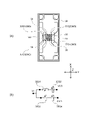
- 6 to 8 are schematic views illustrating the layout of the piezo resistance element. 6 to 8, each (a) shows the layout of the piezo resistance element 35 in a plan view, and (b) shows the circuit diagram of the piezo resistance element 35.
- the sensor substrate 30 has a substantially rectangular shape in a plan view, and the displacement portion 31 is arranged in the central portion.
- the arrow shown indicates the distortion direction SD.
- distortion can be easily detected by making the longitudinal direction (for example, the X direction) substantially parallel to the distortion direction SD.
- FIGS. 6 (a) and 6 (b) show an example of forming a full bridge with a plurality of piezo resistance elements 35. Further, FIGS. 7 (a) and 7 (b), and FIGS. 8 (a) and 8 (b) show an example in which a half bridge is formed by a plurality of piezo resistance elements 35.
- the piezo resistance element 35 constitutes four element groups 35G (first element group 35G1, second element group 35G2, third element group 35G3, and fourth element group 35G4).
- Three piezo resistance elements 35 are provided in one element group 35G, each of which is arranged in parallel in the same direction and electrically connected in series.
- the first element group 35G1 is formed by connecting three piezo resistance elements 35 extending in the Y direction in series.
- the relative arrangement of the four element groups 35G on the sensor substrate 30 is as follows.
- the first element group 35G1 is arranged in the upper left
- the second element group 35G2 is arranged in the upper right
- the third element group 35G3 is arranged in the lower left
- the fourth element group 35G4 is arranged in the lower right.
- the piezo resistance elements 35 of the first element group 35G1 and the fourth element group 35G4 are arranged in a direction orthogonal to the strain direction SD, and the second element group 35G2 and the third element group 35G3 The piezo resistance element 35 is arranged in the distortion direction SD.
- the first element group 35G1 and the third element group 35G3 are electrically connected in series, and the second element group 35G2 and the fourth element group 35G4 are connected in series. Conducts.
- the first element group 35G1 and the third element group 35G3 and the second element group 35G2 and the fourth element group 35G4 conduct in parallel.
- the power supply voltage VDD between the first element group 35G1 and the second element group 35G2, and the ground potential GND between the third element group 35G3 and the fourth element group 35G4.
- the output potential V1 is between the first element group 35G1 and the third element group 35G3, and the output potential V2 is between the second element group 35G2 and the fourth element group 35G4.
- the piezo resistance element 35 of the first element group 35G1 is arranged in a direction orthogonal to the strain direction SD, and the second element group 35G2, the third element group 35G3, and the fourth element group 35G4 The piezo resistance element 35 is arranged in the distortion direction SD.
- the first element group 35G1 and the second element group 35G2 are electrically connected in series, and the third element group 35G3 and the fourth element group 35G4 are connected in series. Conducts.
- the second element group 35G2 side has the power supply voltage VDD, and the first element group 35G1 has the output potential V1.
- the fourth element group 35G4 side has the ground potential GND.
- the first element group 35G1 and the second element group 35G2 are reference resistances
- the third element group 35G3 and the fourth element group 35G4 are sensor resistances.
- the piezo resistance elements 35 of the first element group 35G1 and the second element group 35G2 are arranged in a direction orthogonal to the strain direction SD, and the third element group 35G3 and the fourth element group 35G4 are arranged.
- the piezo resistance element 35 is arranged in the distortion direction SD.
- the first element group 35G1 and the second element group 35G2 are electrically connected in series, and the third element group 35G3 and the fourth element group 35G4 are connected in series. Conducts.
- the second element group 35G2 side has the power supply voltage VDD, and the first element group 35G1 has the output potential V1.
- the fourth element group 35G4 side has the ground potential GND.
- the resistance values of the first element group 35G1 and the second element group 35G2 decrease with respect to the strain, and the resistance values of the third element group 35G3 and the fourth element group 35G4 increase. Therefore, in the half-bridge configuration shown in FIG. 8, the output value is larger than that in the half-bridge configuration shown in FIG. 7.
- FIG. 9 is a diagram showing the relationship between the exposure height of the sensor substrate in the strain sensor and the amount of sensor strain.
- the horizontal axis shows the exposure height (micrometer: ⁇ m) of the surface 30a of the sensor substrate 30 from the surface 40a of the mold resin 40
- the vertical axis shows the strain amount (microstrain: ⁇ st).
- the strain amount on the vertical axis is a simulation result of the strain amount of the sensor substrate 30 when 14.3 kilonewtons (kN) are added to the strain generator 100 in the X direction.
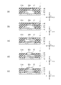
- 10 (a) to 10 (e) are schematic views illustrating an exposed state of the sensor substrate.
- the exposed state of the sensor substrate 30 shown in FIGS. 10A to 10E corresponds to the exposure height at the plot positions shown in FIGS. 9A to 9E.
- the exposed height of the sensor substrate 30 is set by changing the thickness of the mold resin 40 without changing the thickness of the sensor substrate 30. Further, the thickness of the adhesive layer 80 between the surface 40a of the mold resin 40 and the strain-causing body 100 is constant at 0.11 mm (mm).
- the amount of strain is 34.0 ⁇ st at the exposure height of -100 ⁇ m shown in FIGS. 9 (a) and 10 (a), and the strain is distorted at the exposure height of -50 ⁇ m shown in FIGS. 9 (b) and 10 (b).
- the amount of strain is 39.2 ⁇ st.
- the strain amount is 42.0 ⁇ st at the exposure height +50 ⁇ m shown in FIGS. 9 (d) and 10 (d), and the strain amount is 53 at the exposure height +100 ⁇ m shown in FIGS. 9 (e) and 10 (e). It is 0 ⁇ st.
- the amount of distortion increases as the exposure height of the surface 30a of the sensor substrate 30 from the surface 40a of the mold resin 40 increases (the detection sensitivity increases), and when the exposure height exceeds +50 ⁇ m, the amount of distortion further increases. (The detection sensitivity is higher).
- the thickness of the mold resin 40 is made too thin in order to increase the exposed height of the sensor substrate 30, the loop portion of the first bonding wire 61 and the like may be exposed from the mold resin 40. Therefore, it is desirable that the thickness of the mold resin 40 increases the exposed height of the sensor substrate 30 at a thickness at which the first bonding wire 61 is not exposed.
- the surface 30a of the sensor substrate 30 protrudes from the surface 40a of the mold resin 40, and the surface 40a of the mold resin 40 and the surface 30a of the sensor substrate 30 are the mounting surfaces of the strain-generating body 100.
- This makes it easier for the sensor board 30 to detect the strain from the strain-causing body 100 while firmly fixing it to the strain-causing body 100 around the sensor substrate 30. Therefore, it is possible to provide a strain sensor 1 having a configuration that makes it easy to detect the strain of the strain-causing body 100.
Landscapes
- Physics & Mathematics (AREA)
- General Physics & Mathematics (AREA)
- Measurement Of Length, Angles, Or The Like Using Electric Or Magnetic Means (AREA)
Abstract
対象物の歪みを検知しやすい本発明の歪みセンサは、一態様において、起歪体の歪みを検知する歪みセンサであって、パッケージ基板と、パッケージ基板の上に配置され、電気配線部を有するベース基板と、ベース基板の上に配置され、複数のピエゾ抵抗素子を有するセンサ基板と、パッケージ基板上のベース基板およびセンサ基板を覆うモールド樹脂と、を備え、センサ基板の表面がモール樹脂の表面よりも突出し、モール樹脂の表面およびセンサ基板の表面が起歪体との取り付け面となる。
Description
本発明は、歪みセンサに関し、より詳しくは、対象物に力が印加された際の歪みを検知する歪みセンサに関するものである。
歪みセンサとして、特許文献1には、特定方向のひずみを少ない誤差で測定する力学量測定装置が開示される。この力学量測定装置では、半導体力学量測定装置のシリコン基板において、例えば、測定方向の基板長さに対する基板厚の比を小さく、測定方向に対して垂直な方向の基板長さに対する基板厚の比を大きくしている。
また、特許文献2には、電磁誘導もしくはマイクロ波で回路動作電力を供給した場合でもノイズの影響を受けにくく、精度の高い測定を可能とした力学量測定装置が開示される。この力学量測定装置では、接着部を被測定物に接着することによってひずみの計測を計測している。
対象物の微小な歪みを高精度に検知するためには、起歪体の歪みを効果的に歪みセンサへ伝える必要がある。対象物が小さくなるほど歪みセンサを取り付けるための領域が制限されることから、効果的に歪みを伝えることが困難となる。
本発明はこのような実情に鑑みてなされたものであり、対象物の歪みを検知しやすい構成の歪みセンサを提供することを目的とする。
本発明の一態様は、起歪体の歪みを検知する歪みセンサであって、パッケージ基板と、パッケージ基板の上に配置され、電気配線部を有するベース基板と、ベース基板の上に配置され、複数のピエゾ抵抗素子を有するセンサ基板と、パッケージ基板上のベース基板およびセンサ基板を覆うモールド樹脂と、を備え、センサ基板の表面がモール樹脂の表面よりも突出し、モールド樹脂の表面およびセンサ基板の表面が起歪体との取り付け面となる、ことを特徴とする歪みセンサである。
このように、センサ基板の表面がモールド樹脂の表面よりも突出し、モールド樹脂の表面とセンサ基板の表面が起歪体との取り付け面となることによって、センサ基板の周辺でしっかり起歪体に固定しつつ、起歪体からの歪みを検知しやすくする。
上記歪みセンサにおいて、センサ基板はモールド樹脂と別体に設けられていてもよい。このように、突出しているセンサ基板と封止しているモールド樹脂とが別体設けられていることで、モールド樹脂で覆われている部分は固定されて、センサ基板は歪みを検知しやすくする。
上記歪みセンサにおいて、センサ基板のヤング率は、モールド樹脂のヤング率よりも高いことが好ましい。センサ基板のヤング率の方がモールド樹脂のヤング率よりも高くなることで、モールド樹脂の方が柔らかいため歪んだ際に起歪体と一緒に動いて歪みやすくなる。
上記歪みセンサにおいて、センサ基板の長手方向は、起歪体の歪み方向と略平行であることが好ましい。このように、センサ基板の長手方向が起歪体の歪み方向と平行になることによってより歪みを検知しやすくする。
上記歪みセンサにおいて、モールド樹脂の表面と起歪体との間に接着剤層が設けられていることが好ましい。これにより、接着剤層によって歪みセンサを起歪体に取り付ける際にモールド樹脂の表面において固定できるようになる。
上記歪みセンサにおいて、モールド樹脂の表面と起歪体との間、およびセンサ基板の表面と起歪体との間に接着剤層が設けられ、センサ基板の表面から起歪体までの接着剤層の厚さは、モールド樹脂の表面から起歪体までの接着剤層の厚さよりも薄いことが好ましい。これにより、接着剤層によって歪みセンサを起歪体に取り付ける際にモールド樹脂の表面とセンサ基板の表面とにおいて確実に固定できるとともに、センサ基板に歪みが伝わる際の接着剤層による減衰が抑制され、歪みを検知しやすくなる。
上記歪みセンサにおいて、パッケージ基板とベース基板との間に、センサ基板から出力された信号を処理する信号処理回路を有する回路基板が設けられていてもよい。このように、回路基板もモールド樹脂によって封止されていることによって回路基板を保護することができるとともに、回路基板を含めて1つのパッケージに収容され、設置スペースを小さくすることができる。
本発明によれば、対象物の歪みを検知しやすい構成の歪みセンサを提供することが可能となる。
以下、本発明の実施の形態について添付図面を参照して詳細に説明する。なお、以下の説明では、同一の部材には同一の符号を付し、一度説明した部材については適宜その説明を省略する。
(歪みセンサの構成)
図1は、本実施形態に係る歪みセンサの構成を例示する斜視図である。
図2は、本実施形態に係る歪みセンサの構成を例示する断面図である。
図3は、センサ基板を例示する分解斜視図である。
なお、図1では、モールド樹脂40を透視した状態が示される。また、図2では、図1に示すA-A断面が示される。また、図3(a)にはセンサ基板30の表面側からの分解斜視図が示され、図3(b)にはセンサ基板30の裏面側からの分解斜視図が示される。
図1は、本実施形態に係る歪みセンサの構成を例示する斜視図である。
図2は、本実施形態に係る歪みセンサの構成を例示する断面図である。
図3は、センサ基板を例示する分解斜視図である。
なお、図1では、モールド樹脂40を透視した状態が示される。また、図2では、図1に示すA-A断面が示される。また、図3(a)にはセンサ基板30の表面側からの分解斜視図が示され、図3(b)にはセンサ基板30の裏面側からの分解斜視図が示される。
本実施形態は、起歪体の歪みを検知する歪みセンサ1であって、パッケージ基板10と、ベース基板20と、センサ基板30と、モールド樹脂40とを備える。なお、実施形態の説明では、パッケージ基板10の基板実装面10aの法線方向をZ方向、法線方向(Z方向)に直交する方向の1つをX方向、他の1つをY方向とする。
パッケージ基板10は、モールド樹脂40とともに歪みセンサ1の外観を構成する部分であり、歪みセンサ1における底面側に設けられる基板である。Z方向にみた平面視におけるパッケージ基板10の大きさは、縦約2ミリメートル(mm)×横約2mm程度である。
パッケージ基板10は、ベース基板20を実装する基板実装面10aと、基板実装面10aとは反対側に設けられるパッド面10bと、を有する。パッケージ基板10における基板実装面10aの延長面上にはパッド部16が設けられる。パッケージ基板10のパッド面10bには、外部と導通を得るために複数の電極端子11が設けられる。この電極端子11によって外部(例えば、フレキシブル基板F(後述の図4参照))との接続および導通が行われる。
ベース基板20は、パッケージ基板10の上に配置される(Z方向に積層される)。ベース基板20は、センサ基板30を実装するセンサ実装面20aを有する。また、ベース基板20は、センサ基板30に設けられた複数のピエゾ抵抗素子35のそれぞれと電気的に接続する電気配線部25を有する。
センサ基板30は、ベース基板20の上に配置される(Z方向に積層される)。センサ基板30は、変位部31およびピエゾ抵抗素子35を有する。センサ基板30は、Z方向にみた平面視において略長方形となっており、中央部分に変位部31が設けられる。変位部31は、起歪体100の歪みを受けて変位する部分であり、センサ基板30のベース基板20側の面に設けられる。ピエゾ抵抗素子35は、変位部31の変位量を電気的に検出する素子である。
パッケージ基板10とベース基板20との間には回路基板50が設けられていてもよい。回路基板50は、センサ基板30から出力された信号を処理する信号処理回路(信号処理用IC)を有する。回路基板50が設けられている場合、ベース基板20と回路基板50とが第1ボンディングワイヤ61によって導通し、回路基板50とパッケージ基板10とが第2ボンディングワイヤ62によって導通する状態となる。
モールド樹脂40は、パッケージ基板10上のベース基板20およびセンサ基板30を覆う封止樹脂である。モールド樹脂40は、樹脂のみから構成されていてもよいし、無機材料などからなるフィラー成分を有していてもよい。モールド樹脂40は、パッケージ基板10とともに歪みセンサ1の外観を構成する部分である。回路基板50が設けられている場合には、ベース基板20およびセンサ基板30とともに回路基板50もモールド樹脂40によって覆われる。
このような構成を備えた本実施形態に係る歪みセンサ1では、センサ基板30の表面30aがモールド樹脂40の表面40aよりも突出し、モールド樹脂40の表面40aおよびセンサ基板30の表面30aが起歪体100(後述の図4参照)との取り付け面となる。このように、センサ基板30の表面30aがモールド樹脂40の表面40aよりも突出し、モールド樹脂40の表面40aとセンサ基板30の表面30aが起歪体100との取り付け面となることによって、センサ基板30の周辺でしっかり起歪体100に固定しつつ、起歪体100からの歪みを検知しやすくする。
また、本実施形態に係る歪みセンサ1において、センサ基板30はモールド樹脂40と別体に設けられていることが好ましい。これにより、センサ基板30の変形とモールド樹脂40の変形とが干渉しにくくなるため、モールド樹脂40で覆われている部分が固定されていても、センサ基板30は歪みを検知しやすくする。
また、センサ基板30のヤング率は、モールド樹脂40のヤング率よりも高いことが好ましい。センサ基板30のヤング率の方がモールド樹脂40のヤング率よりも高くなることで、モールド樹脂40の方が柔らかいことになり、起歪体100が歪んだときにモールド樹脂40が一緒に動いて歪みやすくなり、センサ基板30で歪みを検知しやすくなる。また、センサ基板30が起歪体100の歪みに応じて変形する際に、モールド樹脂40が変形抵抗となることも生じにくくなる。ここで、センサ基板30がシリコンなどの半導体から構成されている場合には、そのヤング率は100GPa以上であることから、モールド樹脂40のヤング率は、20GPa以下であることが好ましく、10GPa以下であることがより好ましい。換言すれば、センサ基板30のヤング率に対して、モールド樹脂40のヤング率は、20%以下であることが好ましく、10%以下であることがより好ましい。
(歪みセンサの起歪体への取り付け状態)
図4は、歪みセンサの起歪体への取り付け状態を例示する断面図である。
本実施形態に係る歪みセンサ1は、起歪体100の表面に例えば接着剤層80によって取り付けられる。接着剤層80は例えば樹脂系材料からなり、モールド樹脂40の表面40aと起歪体100との間に設けられる。モールド樹脂40の表面40aの面積は、センサ基板30の表面30aの面積よりも広いため、この表面40aで接着剤層80によって起歪体100と接着されることで、歪みセンサ1を起歪体100へしっかり固定できるようになる。
図4は、歪みセンサの起歪体への取り付け状態を例示する断面図である。
本実施形態に係る歪みセンサ1は、起歪体100の表面に例えば接着剤層80によって取り付けられる。接着剤層80は例えば樹脂系材料からなり、モールド樹脂40の表面40aと起歪体100との間に設けられる。モールド樹脂40の表面40aの面積は、センサ基板30の表面30aの面積よりも広いため、この表面40aで接着剤層80によって起歪体100と接着されることで、歪みセンサ1を起歪体100へしっかり固定できるようになる。
本実施形態に係る歪みセンサ1において、センサ基板30の長手方向(例えば、X方向)は、起歪体100の歪み方向SDと略平行であることが好ましい。これにより、センサ基板30によって起歪体100の歪みを受けやすくなり、歪みセンサ1での歪み検知が行いやすくなる。
また、接着剤層80は、モールド樹脂40の表面40aから突出するセンサ基板30の表面30aと起歪体100との間に設けられていてもよい。接着剤層80におけるセンサ基板30の表面30aと起歪体100との間の部分を第1部分80a、モールド樹脂40の表面40aと起歪体100との間の部分を第2部分80bとして、第1部分80aの厚さt1(センサ基板30の表面30aから起歪体100までの接着剤層80の厚さt1)は、第2部分80bの厚さt2(モールド樹脂40の表面40aから起歪体100までの接着剤層80の厚さt2)よりも薄くなる。
これにより、接着剤層80によって歪みセンサ1を起歪体100に取り付ける際に、接着剤層80の機能を分けることができる。すなわち、モールド樹脂40の表面40aと起歪体100の表面との間に位置する接着剤層80の第2部分80bは相対的に厚いため、歪みセンサ1を起歪体100に対して確実に固定することができる。起歪体100が歪んだ場合には、この相対的に厚い第2部分80bにより歪みを吸収し、第2部分80bとモールド樹脂40との間での剥離を抑制することができる。また、モールド樹脂40はセンサ基板30よりもヤング率が低いため、起歪体100からの歪みがモールド樹脂40に伝達されても、モールド樹脂40においてこの歪みを吸収することが可能である。
一方、センサ基板30の表面30aと起歪体100の表面との間に位置する接着剤層80の第1部分80aは相対的に薄いため、起歪体100の歪みがセンサ基板30に伝わる際に第1部分80aにおいて減衰しにくく、センサ基板30のピエゾ抵抗素子35で歪みを検知しやすくなる。また、センサ基板30よりもその周囲に位置するモールド樹脂40の方がヤング率が低いため、センサ基板30が起歪体100の歪みに応じて変形することに対して、モールド樹脂40は変形抵抗となりにくい。このように、接着剤層80の第1部分80aの厚さと第2部分80bの厚さと異ならせることにより、歪みセンサ1が小型化してその起歪体100への取付面積が小さくなっても、起歪体100が歪んだ際に歪みセンサ1が脱落しにくく、かつ、センサ基板30において起歪体100のその歪みを適切に検出することが実現されている。
なお、第1部分80aと第2部分80bとで互いに接着剤層80の硬さを変えてもよい。この場合、第2部分80bの接着剤層80の硬さに比べ、第1部分80aの接着剤層80の硬さを固くするとよい。これにより、固い接着剤層80を介して起歪体100の歪みをセンサ基板30で検知しやすくなる。接着剤層80の硬さは、その成分を変更する、例えば樹脂成分に加えて硬質なフィラー成分を含有させることによって、適宜調整することが可能である。
一方、製造上の観点からは、第1部分80aと第2部分80bとで同じ接着剤層80を用いるほうが好ましい。この場合、第1部分80aと第2部分80bとで接着剤層80の硬さは同じになる。本実施形態では、第1部分80aの接着剤層80の厚さt1が、第2部分80bの接着剤層80の厚さt2よりも薄くなることから、第1部分80aおよび第2部分80bの両部分の接着剤層80の硬さが同じであっても、起歪体100からの歪みがセンサ基板30に伝わるまでの間で接着剤層80による緩衝作用が弱く、歪みを検知しやすくなる。
特に、本実施形態に係る歪みセンサ1は、平面視サイズ(パッケージ基板10サイズ)として縦横それぞれ2mm程度の微小なものであるため、歪みセンサ1を起歪体100にボルトのような締結部材によって固定することが困難であり、接着剤層80による接着固定が有利となる。接着剤層80による歪みセンサ1の起歪体100への固定では、十分な接着面積が必要となる。本実施形態に係る歪みセンサ1では、製造上有利となる一種類の接着剤層80によって歪みセンサ1を起歪体100に固定する場合でも、歪みセンサ1の起歪体100への確実な固定と、歪みセンサ1による高感度の歪み検知との両立を図ることができる。
(ピエゾ抵抗素子のレイアウト例)
次に、本実施形態に係る歪みセンサ1で適用されるピエゾ抵抗素子35のレイアウト例について説明する。
図5は、変位部とピエゾ抵抗素子との位置関係を例示する模式断面図である。
ベース基板20とセンサ基板30との間にはシール26が設けられる。シール26は金や銀などの金属によって形成されており、センサ基板30をベース基板20上に支持するとともに電気的な接続を行う役目を果たす。センサ基板30におけるベース基板20側の面でシール26の内側の領域に変位部31が設けられる。歪みセンサ1では、複数のピエゾ抵抗素子35は変位部31の内側に配置される。
次に、本実施形態に係る歪みセンサ1で適用されるピエゾ抵抗素子35のレイアウト例について説明する。
図5は、変位部とピエゾ抵抗素子との位置関係を例示する模式断面図である。
ベース基板20とセンサ基板30との間にはシール26が設けられる。シール26は金や銀などの金属によって形成されており、センサ基板30をベース基板20上に支持するとともに電気的な接続を行う役目を果たす。センサ基板30におけるベース基板20側の面でシール26の内側の領域に変位部31が設けられる。歪みセンサ1では、複数のピエゾ抵抗素子35は変位部31の内側に配置される。
図6から図8はピエゾ抵抗素子のレイアウトを例示する模式図である。
なお、図6から図8において、それぞれの(a)にはピエゾ抵抗素子35の平面視のレイアウトが示される、(b)にはピエゾ抵抗素子35の回路図が示される。
なお、図6から図8において、それぞれの(a)にはピエゾ抵抗素子35の平面視のレイアウトが示される、(b)にはピエゾ抵抗素子35の回路図が示される。
センサ基板30は、平面視において略長方形となっており、中央部分に変位部31が配置される。図示する矢印は歪み方向SDを示している。センサ基板30が略長方形の場合、長手方向(例えば、X方向)を歪み方向SDと略平行にすることで歪みを検知しやすくなる。
図6(a)および(b)には、複数のピエゾ抵抗素子35によってフルブリッジを構成する例が示される。また、図7(a)および(b)、図8(a)および(b)には複数のピエゾ抵抗素子35によってハーフブリッジを構成する例が示される。
それぞれの例において、ピエゾ抵抗素子35によって4つの素子群35G(第1素子群35G1、第2素子群35G2、第3素子群35G3および第4素子群35G4)が構成される。1つの素子群35Gには3つのピエゾ抵抗素子35が設けられ、それぞれが同一方向に平行に配置され、電気的に直列に接続される。例えば、図6において、第1素子群35G1は、Y方向に延びる3つのピエゾ抵抗素子35が直列に接続されてなる。4つの素子群35Gのセンサ基板30上の相対配置は次のとおりである。すなわち、第1素子群35G1は左上に配置され、第2素子群35G2は右上に配置され、第3素子群35G3は左下に配置され、第4素子群35G4は右下に配置される。
図6(a)に示す例では、第1素子群35G1および第4素子群35G4のピエゾ抵抗素子35が歪み方向SDと直交する方向に配置され、第2素子群35G2および第3素子群35G3のピエゾ抵抗素子35が歪み方向SDに配置される。
図6(b)に示すように、フルブリッジを構成するため、第1素子群35G1と第3素子群35G3とが直列に導通し、第2素子群35G2と第4素子群35G4とが直列に導通する。第1素子群35G1および第3素子群35G3と、第2素子群35G2および第4素子群35G4とは並列に導通する。第1素子群35G1と第2素子群35G2との間が電源電圧VDD、第3素子群35G3と第4素子群35G4との間が接地電位GNDとなる。また、第1素子群35G1と第3素子群35G3との間が出力電位V1、第2素子群35G2と第4素子群35G4との間が出力電位V2となる。
図7(a)に示す例では、第1素子群35G1のピエゾ抵抗素子35が歪み方向SDと直交する方向に配置され、第2素子群35G2、第3素子群35G3および第4素子群35G4のピエゾ抵抗素子35が歪み方向SDに配置される。
図7(b)に示すように、ハーフブリッジを構成するため、第1素子群35G1と第2素子群35G2とが直列に導通し、第3素子群35G3と第4素子群35G4とが直列に導通する。第1素子群35G1と第2素子群35G2との直列接続のうち第2素子群35G2側が電源電圧VDD、第1素子群35G1が出力電位V1となる。また、第3素子群35G3と第4素子群35G4との直列接続のうち第4素子群35G4側が接地電位GNDとなる。このハーフブリッジ構成では、第1素子群35G1および第2素子群35G2がリファレンス抵抗であり、第3素子群35G3および第4素子群35G4がセンサ抵抗である。
図8(a)に示す例では、第1素子群35G1および第2素子群35G2のピエゾ抵抗素子35が歪み方向SDと直交する方向に配置され、第3素子群35G3および第4素子群35G4のピエゾ抵抗素子35が歪み方向SDに配置される。
図8(b)に示すように、ハーフブリッジを構成するため、第1素子群35G1と第2素子群35G2とが直列に導通し、第3素子群35G3と第4素子群35G4とが直列に導通する。第1素子群35G1と第2素子群35G2との直列接続のうち第2素子群35G2側が電源電圧VDD、第1素子群35G1が出力電位V1となる。また、第3素子群35G3と第4素子群35G4との直列接続のうち第4素子群35G4側が接地電位GNDとなる。このハーフブリッジ構成では、歪みに対して第1素子群35G1および第2素子群35G2の抵抗値が下がり、第3素子群35G3および第4素子群35G4の抵抗値が上がる。このため、図8に示すハーフブリッジ構成では、図7に示すハーフブリッジ構成よりも出力値が大きくなる。
(歪みセンサの特性)
次に、本実施形態に係る歪みセンサの特性について説明する。
図9は、歪みセンサにおけるセンサ基板の露出高さとセンサ歪み量との関係を示す図である。
図9における横軸はセンサ基板30の表面30aのモールド樹脂40の表面40aからの露出高さ(マイクロメートル:μm)を示し、縦軸は歪み量(マイクロストレイン:μst)を示している。縦軸の歪み量は、起歪体100にX方向に14.3キロニュートン(kN)を加えたときのセンサ基板30の歪み量のシミュレーション結果である。
図10(a)から(e)は、センサ基板の露出状態を例示する模式図である。
図10(a)から(e)に示すセンサ基板30の露出状態は、図9(a)から(e)に示すプロット位置での露出高さに対応している。
次に、本実施形態に係る歪みセンサの特性について説明する。
図9は、歪みセンサにおけるセンサ基板の露出高さとセンサ歪み量との関係を示す図である。
図9における横軸はセンサ基板30の表面30aのモールド樹脂40の表面40aからの露出高さ(マイクロメートル:μm)を示し、縦軸は歪み量(マイクロストレイン:μst)を示している。縦軸の歪み量は、起歪体100にX方向に14.3キロニュートン(kN)を加えたときのセンサ基板30の歪み量のシミュレーション結果である。
図10(a)から(e)は、センサ基板の露出状態を例示する模式図である。
図10(a)から(e)に示すセンサ基板30の露出状態は、図9(a)から(e)に示すプロット位置での露出高さに対応している。
ここで、センサ基板30の露出高さについては、センサ基板30の厚さを変えず、モールド樹脂40の厚さを変えることによって設定している。また、モールド樹脂40の表面40aと起歪体100との間の接着剤層80の厚さは0.11ミリメートル(mm)で一定としている。
シミュレーションの結果、図9(a)および図10(a)に示す露出高さ-100μmでは歪み量が34.0μst、図9(b)および図10(b)に示す露出高さ-50μmでは歪み量が36.9μst、図5(c)および図6(c)に示す露出高さ0μmでは歪み量が39.2μstである。
また、図9(d)および図10(d)に示す露出高さ+50μmでは歪み量が42.0μst、図9(e)および図10(e)に示す露出高さ+100μmでは歪み量が53.0μstである。
このように、センサ基板30の表面30aのモールド樹脂40の表面40aからの露出高さが増加するほど歪み量が増加し(検知感度が高まる)、露出高さ+50μmを越えるとより歪み量が増加する(検知感度がより高まる)ことが分かる。
なお、センサ基板30の露出高さを増やすためにモールド樹脂40の厚さを薄くし過ぎると、第1ボンディングワイヤ61のループ部分などがモールド樹脂40から露出する可能性がある。したがって、モールド樹脂40の厚さは、第1ボンディングワイヤ61が露出しない厚さにおいてセンサ基板30の露出高さを高くすることが望ましい。
このように、本実施形態によれば、センサ基板30の表面30aがモールド樹脂40の表面40aよりも突出し、モールド樹脂40の表面40aとセンサ基板30の表面30aが起歪体100との取り付け面となることによって、センサ基板30の周辺でしっかり起歪体100に固定しつつ、起歪体100からの歪みをセンサ基板30によって検知しやすくなる。したがって、起歪体100の歪みを検知しやすい構成の歪みセンサ1を提供することが可能となる。
なお、上記に本実施形態を説明したが、本発明はこれらの例に限定されるものではない。例えば、前述の各実施形態に対して、当業者が適宜、構成要素の追加、削除、設計変更を行ったものや、各実施形態の構成例の特徴を適宜組み合わせたものも、本発明の要旨を備えている限り、本発明の範囲に含有される。
1…歪みセンサ
10…パッケージ基板
10a…基板実装面
10b…パッド面
11…電極端子
16…パッド部
20…ベース基板
20a…センサ実装面
25…電気配線部
26…シール
30…センサ基板
30a…表面
31…変位部
35…ピエゾ抵抗素子
35G…素子群
35G1…第1素子群
35G2…第2素子群
35G3…第3素子群
35G4…第4素子群
40…モールド樹脂
40a…表面
50…回路基板
61…第1ボンディングワイヤ
62…第2ボンディングワイヤ
80…接着剤層
80a…第1部分
80b…第2部分
100…起歪体
F…フレキシブル基板
GND…接地電位
SD…歪み方向
V1…出力電位
V2…出力電位
VDD…電源電圧
t1…第1部分の厚さ
t2…第2部分の厚さ
10…パッケージ基板
10a…基板実装面
10b…パッド面
11…電極端子
16…パッド部
20…ベース基板
20a…センサ実装面
25…電気配線部
26…シール
30…センサ基板
30a…表面
31…変位部
35…ピエゾ抵抗素子
35G…素子群
35G1…第1素子群
35G2…第2素子群
35G3…第3素子群
35G4…第4素子群
40…モールド樹脂
40a…表面
50…回路基板
61…第1ボンディングワイヤ
62…第2ボンディングワイヤ
80…接着剤層
80a…第1部分
80b…第2部分
100…起歪体
F…フレキシブル基板
GND…接地電位
SD…歪み方向
V1…出力電位
V2…出力電位
VDD…電源電圧
t1…第1部分の厚さ
t2…第2部分の厚さ
Claims (7)
- 起歪体の歪みを検知する歪みセンサであって、
パッケージ基板と、
前記パッケージ基板の上に配置され、電気配線部を有するベース基板と、
前記ベース基板の上に配置され、複数のピエゾ抵抗素子を有するセンサ基板と、
前記パッケージ基板上の前記ベース基板および前記センサ基板を覆うモールド樹脂と、
を備え、
前記センサ基板の表面が前記モールド樹脂の表面よりも突出し、前記モールド樹脂の表面および前記センサ基板の表面が前記起歪体との取り付け面となる、ことを特徴とする歪みセンサ。 - 前記センサ基板は前記モールド樹脂と別体に設けられた、請求項1記載の歪みセンサ。
- 前記センサ基板のヤング率は、前記モールド樹脂のヤング率よりも高い、請求項1または請求項2に記載の歪みセンサ。
- 前記センサ基板の長手方向は、前記起歪体の歪み方向と略平行である、請求項1から請求項3のいずれか1項に記載の歪みセンサ。
- 前記モールド樹脂の表面と前記起歪体との間に接着剤層が設けられた、請求項1から請求項4のいずれか1項に記載の歪みセンサ。
- 前記モールド樹脂の表面と前記起歪体との間、および前記センサ基板の表面と前記起歪体との間に接着剤層が設けられ、
前記センサ基板の表面から前記起歪体までの前記接着剤層の厚さは、前記モールド樹脂の表面から前記起歪体までの前記接着剤層の厚さよりも薄い、請求項1から請求項4のいずれか1項に記載の歪みセンサ。 - 前記パッケージ基板と前記ベース基板との間に、前記センサ基板から出力された信号を処理する信号処理回路を有する回路基板が設けられた、請求項1から請求項6のいずれか1項に記載の歪みセンサ。
Applications Claiming Priority (2)
| Application Number | Priority Date | Filing Date | Title |
|---|---|---|---|
| JP2020211702A JP2024012731A (ja) | 2020-12-21 | 2020-12-21 | 歪みセンサ |
| JP2020-211702 | 2020-12-21 |
Publications (1)
| Publication Number | Publication Date |
|---|---|
| WO2022137828A1 true WO2022137828A1 (ja) | 2022-06-30 |
Family
ID=82157559
Family Applications (1)
| Application Number | Title | Priority Date | Filing Date |
|---|---|---|---|
| PCT/JP2021/040717 Ceased WO2022137828A1 (ja) | 2020-12-21 | 2021-11-05 | 歪みセンサ |
Country Status (2)
| Country | Link |
|---|---|
| JP (1) | JP2024012731A (ja) |
| WO (1) | WO2022137828A1 (ja) |
Citations (4)
| Publication number | Priority date | Publication date | Assignee | Title |
|---|---|---|---|---|
| JP2010073765A (ja) * | 2008-09-17 | 2010-04-02 | Renesas Technology Corp | 半導体装置およびその製造方法 |
| JP2011220865A (ja) * | 2010-04-09 | 2011-11-04 | Alps Electric Co Ltd | フォースセンサパッケージ及びその製造方法 |
| US20170057810A1 (en) * | 2015-09-01 | 2017-03-02 | Apple Inc. | Strain Reduction and Sensing on Package Substrates |
| US20190252556A1 (en) * | 2018-02-13 | 2019-08-15 | Stmicroelectronics S.R.L. | Load sensing devices, packages, and systems |
-
2020
- 2020-12-21 JP JP2020211702A patent/JP2024012731A/ja active Pending
-
2021
- 2021-11-05 WO PCT/JP2021/040717 patent/WO2022137828A1/ja not_active Ceased
Patent Citations (4)
| Publication number | Priority date | Publication date | Assignee | Title |
|---|---|---|---|---|
| JP2010073765A (ja) * | 2008-09-17 | 2010-04-02 | Renesas Technology Corp | 半導体装置およびその製造方法 |
| JP2011220865A (ja) * | 2010-04-09 | 2011-11-04 | Alps Electric Co Ltd | フォースセンサパッケージ及びその製造方法 |
| US20170057810A1 (en) * | 2015-09-01 | 2017-03-02 | Apple Inc. | Strain Reduction and Sensing on Package Substrates |
| US20190252556A1 (en) * | 2018-02-13 | 2019-08-15 | Stmicroelectronics S.R.L. | Load sensing devices, packages, and systems |
Also Published As
| Publication number | Publication date |
|---|---|
| JP2024012731A (ja) | 2024-01-31 |
Similar Documents
| Publication | Publication Date | Title |
|---|---|---|
| US6463804B2 (en) | Acceleration sensor | |
| JP5487672B2 (ja) | 物理量センサ | |
| US20100179430A1 (en) | Ultrasonic probe and method for manufacturing the same and ultrasonic diagnostic device | |
| US20120133042A1 (en) | Mounting structure of chip and module using the same | |
| JP5990933B2 (ja) | 圧力センサパッケージの製造方法 | |
| JP2008039760A (ja) | 圧力センサ | |
| JP6293982B2 (ja) | 力学量測定装置 | |
| JP4892781B2 (ja) | 半導体物理量センサ | |
| US20250117099A1 (en) | Ultrasonic touch sensor | |
| CN110160681B (zh) | 负荷感测装置、封装件以及系统 | |
| CN101960590B (zh) | 用于直接引线结合到可编程补偿集成电路管芯的压力感测管芯焊盘布局和方法 | |
| KR20040097929A (ko) | 가속도 센서 장치 | |
| JP2006078249A (ja) | 容量型半導体センサ | |
| TWI693382B (zh) | 力量感測器 | |
| JP2024012731A (ja) | 歪みセンサ | |
| JP2010147227A (ja) | 電子デバイスパッケージ | |
| US20150082898A1 (en) | Strain sensor | |
| JP3528834B2 (ja) | 加速度センサ | |
| JP4706634B2 (ja) | 半導体センサおよびその製造方法 | |
| CN111473893A (zh) | 力量传感器 | |
| JP7795071B2 (ja) | 耐塵埃/耐ノイズ構造を有するセンサ | |
| JP4399545B2 (ja) | 触覚センサおよび多点型触覚センサ | |
| JP4393322B2 (ja) | 半導体圧力センサ | |
| JP2010071817A (ja) | 半導体センサ内蔵パッケージ | |
| KR20110059028A (ko) | 반도체 스트레인게이지형 압력센서모듈과 그 제조방법 |
Legal Events
| Date | Code | Title | Description |
|---|---|---|---|
| 121 | Ep: the epo has been informed by wipo that ep was designated in this application |
Ref document number: 21909982 Country of ref document: EP Kind code of ref document: A1 |
|
| NENP | Non-entry into the national phase |
Ref country code: DE |
|
| 122 | Ep: pct application non-entry in european phase |
Ref document number: 21909982 Country of ref document: EP Kind code of ref document: A1 |
|
| NENP | Non-entry into the national phase |
Ref country code: JP |