WO2022131273A1 - セラミックススクライブ基板、セラミックス基板、セラミックススクライブ基板の製造方法、セラミックス基板の製造方法、セラミックス回路基板の製造方法、及び、半導体素子の製造方法 - Google Patents
セラミックススクライブ基板、セラミックス基板、セラミックススクライブ基板の製造方法、セラミックス基板の製造方法、セラミックス回路基板の製造方法、及び、半導体素子の製造方法 Download PDFInfo
- Publication number
- WO2022131273A1 WO2022131273A1 PCT/JP2021/046148 JP2021046148W WO2022131273A1 WO 2022131273 A1 WO2022131273 A1 WO 2022131273A1 JP 2021046148 W JP2021046148 W JP 2021046148W WO 2022131273 A1 WO2022131273 A1 WO 2022131273A1
- Authority
- WO
- WIPO (PCT)
- Prior art keywords
- ceramic
- substrate
- scribe
- manufacturing
- circuit board
- Prior art date
- Legal status (The legal status is an assumption and is not a legal conclusion. Google has not performed a legal analysis and makes no representation as to the accuracy of the status listed.)
- Ceased
Links
Images


Classifications
-
- C—CHEMISTRY; METALLURGY
- C04—CEMENTS; CONCRETE; ARTIFICIAL STONE; CERAMICS; REFRACTORIES
- C04B—LIME, MAGNESIA; SLAG; CEMENTS; COMPOSITIONS THEREOF, e.g. MORTARS, CONCRETE OR LIKE BUILDING MATERIALS; ARTIFICIAL STONE; CERAMICS; REFRACTORIES; TREATMENT OF NATURAL STONE
- C04B35/00—Shaped ceramic products characterised by their composition; Ceramics compositions; Processing powders of inorganic compounds preparatory to the manufacturing of ceramic products
- C04B35/515—Shaped ceramic products characterised by their composition; Ceramics compositions; Processing powders of inorganic compounds preparatory to the manufacturing of ceramic products based on non-oxide ceramics
-
- H—ELECTRICITY
- H10—SEMICONDUCTOR DEVICES; ELECTRIC SOLID-STATE DEVICES NOT OTHERWISE PROVIDED FOR
- H10W—GENERIC PACKAGES, INTERCONNECTIONS, CONNECTORS OR OTHER CONSTRUCTIONAL DETAILS OF DEVICES COVERED BY CLASS H10
- H10W74/00—Encapsulations, e.g. protective coatings
- H10W74/10—Encapsulations, e.g. protective coatings characterised by their shape or disposition
- H10W74/111—Encapsulations, e.g. protective coatings characterised by their shape or disposition the semiconductor body being completely enclosed
- H10W74/127—Encapsulations, e.g. protective coatings characterised by their shape or disposition the semiconductor body being completely enclosed characterised by arrangements for sealing or adhesion
-
- C—CHEMISTRY; METALLURGY
- C04—CEMENTS; CONCRETE; ARTIFICIAL STONE; CERAMICS; REFRACTORIES
- C04B—LIME, MAGNESIA; SLAG; CEMENTS; COMPOSITIONS THEREOF, e.g. MORTARS, CONCRETE OR LIKE BUILDING MATERIALS; ARTIFICIAL STONE; CERAMICS; REFRACTORIES; TREATMENT OF NATURAL STONE
- C04B35/00—Shaped ceramic products characterised by their composition; Ceramics compositions; Processing powders of inorganic compounds preparatory to the manufacturing of ceramic products
- C04B35/515—Shaped ceramic products characterised by their composition; Ceramics compositions; Processing powders of inorganic compounds preparatory to the manufacturing of ceramic products based on non-oxide ceramics
- C04B35/58—Shaped ceramic products characterised by their composition; Ceramics compositions; Processing powders of inorganic compounds preparatory to the manufacturing of ceramic products based on non-oxide ceramics based on borides, nitrides, i.e. nitrides, oxynitrides, carbonitrides or oxycarbonitrides or silicides
-
- C—CHEMISTRY; METALLURGY
- C04—CEMENTS; CONCRETE; ARTIFICIAL STONE; CERAMICS; REFRACTORIES
- C04B—LIME, MAGNESIA; SLAG; CEMENTS; COMPOSITIONS THEREOF, e.g. MORTARS, CONCRETE OR LIKE BUILDING MATERIALS; ARTIFICIAL STONE; CERAMICS; REFRACTORIES; TREATMENT OF NATURAL STONE
- C04B35/00—Shaped ceramic products characterised by their composition; Ceramics compositions; Processing powders of inorganic compounds preparatory to the manufacturing of ceramic products
- C04B35/515—Shaped ceramic products characterised by their composition; Ceramics compositions; Processing powders of inorganic compounds preparatory to the manufacturing of ceramic products based on non-oxide ceramics
- C04B35/58—Shaped ceramic products characterised by their composition; Ceramics compositions; Processing powders of inorganic compounds preparatory to the manufacturing of ceramic products based on non-oxide ceramics based on borides, nitrides, i.e. nitrides, oxynitrides, carbonitrides or oxycarbonitrides or silicides
- C04B35/581—Shaped ceramic products characterised by their composition; Ceramics compositions; Processing powders of inorganic compounds preparatory to the manufacturing of ceramic products based on non-oxide ceramics based on borides, nitrides, i.e. nitrides, oxynitrides, carbonitrides or oxycarbonitrides or silicides based on aluminium nitride
-
- C—CHEMISTRY; METALLURGY
- C04—CEMENTS; CONCRETE; ARTIFICIAL STONE; CERAMICS; REFRACTORIES
- C04B—LIME, MAGNESIA; SLAG; CEMENTS; COMPOSITIONS THEREOF, e.g. MORTARS, CONCRETE OR LIKE BUILDING MATERIALS; ARTIFICIAL STONE; CERAMICS; REFRACTORIES; TREATMENT OF NATURAL STONE
- C04B35/00—Shaped ceramic products characterised by their composition; Ceramics compositions; Processing powders of inorganic compounds preparatory to the manufacturing of ceramic products
- C04B35/515—Shaped ceramic products characterised by their composition; Ceramics compositions; Processing powders of inorganic compounds preparatory to the manufacturing of ceramic products based on non-oxide ceramics
- C04B35/58—Shaped ceramic products characterised by their composition; Ceramics compositions; Processing powders of inorganic compounds preparatory to the manufacturing of ceramic products based on non-oxide ceramics based on borides, nitrides, i.e. nitrides, oxynitrides, carbonitrides or oxycarbonitrides or silicides
- C04B35/584—Shaped ceramic products characterised by their composition; Ceramics compositions; Processing powders of inorganic compounds preparatory to the manufacturing of ceramic products based on non-oxide ceramics based on borides, nitrides, i.e. nitrides, oxynitrides, carbonitrides or oxycarbonitrides or silicides based on silicon nitride
-
- C—CHEMISTRY; METALLURGY
- C04—CEMENTS; CONCRETE; ARTIFICIAL STONE; CERAMICS; REFRACTORIES
- C04B—LIME, MAGNESIA; SLAG; CEMENTS; COMPOSITIONS THEREOF, e.g. MORTARS, CONCRETE OR LIKE BUILDING MATERIALS; ARTIFICIAL STONE; CERAMICS; REFRACTORIES; TREATMENT OF NATURAL STONE
- C04B37/00—Joining burned ceramic articles with other burned ceramic articles or other articles by heating
- C04B37/02—Joining burned ceramic articles with other burned ceramic articles or other articles by heating with metallic articles
- C04B37/023—Joining burned ceramic articles with other burned ceramic articles or other articles by heating with metallic articles characterised by the interlayer used
- C04B37/026—Joining burned ceramic articles with other burned ceramic articles or other articles by heating with metallic articles characterised by the interlayer used consisting of metals or metal salts
-
- C—CHEMISTRY; METALLURGY
- C04—CEMENTS; CONCRETE; ARTIFICIAL STONE; CERAMICS; REFRACTORIES
- C04B—LIME, MAGNESIA; SLAG; CEMENTS; COMPOSITIONS THEREOF, e.g. MORTARS, CONCRETE OR LIKE BUILDING MATERIALS; ARTIFICIAL STONE; CERAMICS; REFRACTORIES; TREATMENT OF NATURAL STONE
- C04B41/00—After-treatment of mortars, concrete, artificial stone or ceramics; Treatment of natural stone
- C04B41/009—After-treatment of mortars, concrete, artificial stone or ceramics; Treatment of natural stone characterised by the material treated
-
- C—CHEMISTRY; METALLURGY
- C04—CEMENTS; CONCRETE; ARTIFICIAL STONE; CERAMICS; REFRACTORIES
- C04B—LIME, MAGNESIA; SLAG; CEMENTS; COMPOSITIONS THEREOF, e.g. MORTARS, CONCRETE OR LIKE BUILDING MATERIALS; ARTIFICIAL STONE; CERAMICS; REFRACTORIES; TREATMENT OF NATURAL STONE
- C04B41/00—After-treatment of mortars, concrete, artificial stone or ceramics; Treatment of natural stone
- C04B41/53—After-treatment of mortars, concrete, artificial stone or ceramics; Treatment of natural stone involving the removal of at least part of the materials of the treated article, e.g. etching, drying of hardened concrete
- C04B41/5338—Etching
-
- C—CHEMISTRY; METALLURGY
- C04—CEMENTS; CONCRETE; ARTIFICIAL STONE; CERAMICS; REFRACTORIES
- C04B—LIME, MAGNESIA; SLAG; CEMENTS; COMPOSITIONS THEREOF, e.g. MORTARS, CONCRETE OR LIKE BUILDING MATERIALS; ARTIFICIAL STONE; CERAMICS; REFRACTORIES; TREATMENT OF NATURAL STONE
- C04B41/00—After-treatment of mortars, concrete, artificial stone or ceramics; Treatment of natural stone
- C04B41/80—After-treatment of mortars, concrete, artificial stone or ceramics; Treatment of natural stone of only ceramics
- C04B41/91—After-treatment of mortars, concrete, artificial stone or ceramics; Treatment of natural stone of only ceramics involving the removal of part of the materials of the treated articles, e.g. etching
-
- H—ELECTRICITY
- H05—ELECTRIC TECHNIQUES NOT OTHERWISE PROVIDED FOR
- H05K—PRINTED CIRCUITS; CASINGS OR CONSTRUCTIONAL DETAILS OF ELECTRIC APPARATUS; MANUFACTURE OF ASSEMBLAGES OF ELECTRICAL COMPONENTS
- H05K3/00—Apparatus or processes for manufacturing printed circuits
- H05K3/0011—Working of insulating substrates or insulating layers
- H05K3/0017—Etching of the substrate by chemical or physical means
- H05K3/0026—Etching of the substrate by chemical or physical means by laser ablation
- H05K3/0029—Etching of the substrate by chemical or physical means by laser ablation of inorganic insulating material
-
- H—ELECTRICITY
- H05—ELECTRIC TECHNIQUES NOT OTHERWISE PROVIDED FOR
- H05K—PRINTED CIRCUITS; CASINGS OR CONSTRUCTIONAL DETAILS OF ELECTRIC APPARATUS; MANUFACTURE OF ASSEMBLAGES OF ELECTRICAL COMPONENTS
- H05K3/00—Apparatus or processes for manufacturing printed circuits
- H05K3/0011—Working of insulating substrates or insulating layers
- H05K3/0044—Mechanical working of the substrate, e.g. drilling or punching
- H05K3/0052—Depaneling, i.e. dividing a panel into circuit boards; Working of the edges of circuit boards
-
- H—ELECTRICITY
- H10—SEMICONDUCTOR DEVICES; ELECTRIC SOLID-STATE DEVICES NOT OTHERWISE PROVIDED FOR
- H10W—GENERIC PACKAGES, INTERCONNECTIONS, CONNECTORS OR OTHER CONSTRUCTIONAL DETAILS OF DEVICES COVERED BY CLASS H10
- H10W70/00—Package substrates; Interposers; Redistribution layers [RDL]
- H10W70/60—Insulating or insulated package substrates; Interposers; Redistribution layers
- H10W70/67—Insulating or insulated package substrates; Interposers; Redistribution layers characterised by their insulating layers or insulating parts
- H10W70/68—Shapes or dispositions thereof
-
- H—ELECTRICITY
- H10—SEMICONDUCTOR DEVICES; ELECTRIC SOLID-STATE DEVICES NOT OTHERWISE PROVIDED FOR
- H10W—GENERIC PACKAGES, INTERCONNECTIONS, CONNECTORS OR OTHER CONSTRUCTIONAL DETAILS OF DEVICES COVERED BY CLASS H10
- H10W70/00—Package substrates; Interposers; Redistribution layers [RDL]
- H10W70/60—Insulating or insulated package substrates; Interposers; Redistribution layers
- H10W70/67—Insulating or insulated package substrates; Interposers; Redistribution layers characterised by their insulating layers or insulating parts
- H10W70/69—Insulating materials thereof
- H10W70/692—Ceramics or glasses
-
- C—CHEMISTRY; METALLURGY
- C04—CEMENTS; CONCRETE; ARTIFICIAL STONE; CERAMICS; REFRACTORIES
- C04B—LIME, MAGNESIA; SLAG; CEMENTS; COMPOSITIONS THEREOF, e.g. MORTARS, CONCRETE OR LIKE BUILDING MATERIALS; ARTIFICIAL STONE; CERAMICS; REFRACTORIES; TREATMENT OF NATURAL STONE
- C04B2237/00—Aspects relating to ceramic laminates or to joining of ceramic articles with other articles by heating
- C04B2237/30—Composition of layers of ceramic laminates or of ceramic or metallic articles to be joined by heating, e.g. Si substrates
- C04B2237/32—Ceramic
- C04B2237/36—Non-oxidic
- C04B2237/366—Aluminium nitride
-
- C—CHEMISTRY; METALLURGY
- C04—CEMENTS; CONCRETE; ARTIFICIAL STONE; CERAMICS; REFRACTORIES
- C04B—LIME, MAGNESIA; SLAG; CEMENTS; COMPOSITIONS THEREOF, e.g. MORTARS, CONCRETE OR LIKE BUILDING MATERIALS; ARTIFICIAL STONE; CERAMICS; REFRACTORIES; TREATMENT OF NATURAL STONE
- C04B2237/00—Aspects relating to ceramic laminates or to joining of ceramic articles with other articles by heating
- C04B2237/30—Composition of layers of ceramic laminates or of ceramic or metallic articles to be joined by heating, e.g. Si substrates
- C04B2237/32—Ceramic
- C04B2237/36—Non-oxidic
- C04B2237/368—Silicon nitride
-
- H—ELECTRICITY
- H05—ELECTRIC TECHNIQUES NOT OTHERWISE PROVIDED FOR
- H05K—PRINTED CIRCUITS; CASINGS OR CONSTRUCTIONAL DETAILS OF ELECTRIC APPARATUS; MANUFACTURE OF ASSEMBLAGES OF ELECTRICAL COMPONENTS
- H05K1/00—Printed circuits
- H05K1/02—Details
- H05K1/03—Use of materials for the substrate
- H05K1/0306—Inorganic insulating substrates, e.g. ceramic, glass
-
- H—ELECTRICITY
- H05—ELECTRIC TECHNIQUES NOT OTHERWISE PROVIDED FOR
- H05K—PRINTED CIRCUITS; CASINGS OR CONSTRUCTIONAL DETAILS OF ELECTRIC APPARATUS; MANUFACTURE OF ASSEMBLAGES OF ELECTRICAL COMPONENTS
- H05K2201/00—Indexing scheme relating to printed circuits covered by H05K1/00
- H05K2201/09—Shape and layout
- H05K2201/09009—Substrate related
- H05K2201/0909—Preformed cutting or breaking line
-
- H—ELECTRICITY
- H10—SEMICONDUCTOR DEVICES; ELECTRIC SOLID-STATE DEVICES NOT OTHERWISE PROVIDED FOR
- H10W—GENERIC PACKAGES, INTERCONNECTIONS, CONNECTORS OR OTHER CONSTRUCTIONAL DETAILS OF DEVICES COVERED BY CLASS H10
- H10W40/00—Arrangements for thermal protection or thermal control
- H10W40/20—Arrangements for cooling
- H10W40/25—Arrangements for cooling characterised by their materials
- H10W40/255—Arrangements for cooling characterised by their materials having a laminate or multilayered structure, e.g. direct bond copper [DBC] ceramic substrates
-
- H—ELECTRICITY
- H10—SEMICONDUCTOR DEVICES; ELECTRIC SOLID-STATE DEVICES NOT OTHERWISE PROVIDED FOR
- H10W—GENERIC PACKAGES, INTERCONNECTIONS, CONNECTORS OR OTHER CONSTRUCTIONAL DETAILS OF DEVICES COVERED BY CLASS H10
- H10W42/00—Arrangements for protection of devices
- H10W42/121—Arrangements for protection of devices protecting against mechanical damage
Definitions
- the embodiments generally relate to a ceramic scribing substrate, a ceramic substrate, a method for manufacturing a ceramic scribing substrate, a method for manufacturing a ceramic substrate, a method for manufacturing a ceramic circuit board, and a method for manufacturing a semiconductor element.
- a silicon nitride substrate having high strength, high toughness, and high heat dissipation has a size of 220 [mm] ⁇ 220 [mm] ⁇ 0.32 [mm] disclosed. (Patent Document 1).
- Patent Document 2 a method of taking a large number of silicon nitride substrates by using a scribe line formed by laser processing is disclosed ( Patent Document 2).
- Patent Document 2 microcracks in the silicon nitride substrate do not occur more than necessary during division due to multi-cavity by laser machining, and scribe line machining for multi-capping is easy and low cost. It can be carried out.
- the substrate before division became large and thin, the problems caused by laser processing the silicon nitride substrate having high strength and high toughness became clear.
- the silicon nitride substrate has high strength, a large force is required to break along the scribe line, so it is necessary to insert the laser deeply in the thickness direction of the silicon nitride substrate.
- the silicon nitride substrate is thin, there is a high possibility that the silicon nitride substrate will be split due to the processing process after forming the scribe line by the laser or the force applied during transportation.
- the embodiment relates to a ceramic substrate having excellent cost performance, which solves such a problem and enables efficient production of a small substrate from a high-strength and thin large ceramic substrate having both heat dissipation and electrical insulation.
- the ceramic scribe substrate according to the embodiment is provided with a continuous groove in which a plurality of grooves are connected by irradiation of a fiber laser on the surface side of the scribe line for forming the ceramic substrate, and the depth of the continuous groove is 50 [ ⁇ m]. It is also large and is within the range of 0.15 times or more and 0.55 times or less of the thickness of the ceramic substrate.
- FIG. 3 is a cross-sectional view showing an example of a scribe cross section of a ceramic scribe substrate according to an embodiment.
- FIG. 2 is an enlarged partial cross-sectional view of portion A in FIG.
- the figure which shows an example of the ceramics circuit board which concerns on embodiment.
- the side view which shows an example of the ceramics circuit board integrated with the resin mold which concerns on embodiment.
- the scribe line provided on the ceramic scribe substrate according to the embodiment is for forming the ceramic substrate, and indicates the scribe line before dividing the ceramic substrate and the scribe line mark after the division (hereinafter, "" Called "scribe line”).
- the scribe line of the ceramic scribe substrate according to the embodiment has a continuous groove in which a plurality of grooves are connected on the surface side by irradiation with a laser, for example, a fiber laser, and the depth of the continuous groove is larger than 50 [ ⁇ m] and It is characterized in that it is 0.15 times or more and 0.55 times or less the thickness of the ceramic substrate.
- the ceramic scribing substrate, the ceramic substrate, the manufacturing method of the ceramic scribing substrate, the manufacturing method of the ceramic substrate, the manufacturing method of the ceramic circuit board, and the manufacturing method of the semiconductor element according to the embodiment will be described in detail.
- FIG. 1 shows a top view of an example of a ceramic substrate according to an embodiment.
- 1 is a ceramic scribe substrate
- 2 is a ceramic multi-piece substrate
- 3 is a scribe line
- 4 is an individual ceramic substrate to be a product
- 5 is a peripheral portion not used as a product.
- the ceramic scribe substrate 1 includes a ceramic multi-layer board 2 capable of acquiring a plurality of ceramic substrates by division, and a ceramic single substrate 2 capable of acquiring one ceramic substrate by division (not shown).
- FIG. 1 shows an example of a multi-ceramic substrate 2 capable of laser scribing a large number of four ceramic substrates 4 vertically and horizontally along a total of six scribe lines 3 of three vertically and horizontally. It is shown.
- the ceramic scribe substrate 1 is not limited to such a multi-ceramic substrate 2, and may be a ceramic single substrate having a scribe line capable of processing one ceramic substrate into a product shape. It may be a ceramic multi-piece board having a scribe line capable of taking a large number of pieces exceeding two in length and width.
- the ceramic scribe substrate 1 has a rectangular shape in the plan view in FIG. 1, it may have a substantially polygonal shape.
- the three-point bending strength can be as high as 600 [MPa] or more, and further 700 [MPa] or more. Further, there are those having a thermal conductivity of 50 [W / m ⁇ K] or more, and further 80 [W / m ⁇ K] or more.
- the thermal conductivity can be as high as 170 [W / m ⁇ K] or more, and further 230 [W / m ⁇ K] or more.
- the ceramic scribing substrate 1 is a silicon nitride substrate
- the ceramic substrate 4 is also a silicon nitride substrate
- the three-point bending strength of the ceramic scribing substrate 1 is the three-point bending of the ceramic substrate 4. It is synonymous with strength and the like.
- These ceramic scribe substrates 1 may be a single plate or may have a three-dimensional structure such as a multilayer structure.
- the scribe line 3 is a laser scribe line processed by a fiber laser.
- the fiber laser conforms to the one defined in JIS-Z 3001-5 (2013) as the fiber laser.
- FIG. 2 shows an example of a scribe cross section of the ceramic scribe substrate 1 according to the embodiment.
- 6 is a laser irradiation surface (surface) which is a surface on the side where laser irradiation is performed
- 7 is a continuous groove in which a plurality of grooves are connected to the surface side by laser irradiation
- 8 is a continuous groove in which a plurality of grooves are connected to the deep side by laser irradiation.
- the non-continuous groove group (plurality of recesses) and 9 are the laser non-irradiated surface (back surface) which is the side not irradiated with the laser and the opposite surface of the laser irradiation surface 6.
- the ceramic scribing substrate 1 is provided with the continuous groove 7 so that the continuous groove 7 is provided on the surface side of the scribing line 3 on at least one side of the scribing line 3 on the four sides of the ceramic substrate 4 formed by the ceramic scribing substrate 1. good.
- FIG. 3 is an enlargement of the cross section of the part A in FIG. T is the thickness of the ceramic scribe substrate 1
- D1 is the distance from the surface of the ceramic scribe substrate 1 to the deepest part of the continuous groove 7 (depth of the continuous groove 7)
- D2 is the discontinuous groove group from the deepest part of the continuous groove 7.
- the distance to the deepest part of 8 (the depth of the discontinuous groove group 8) is shown.
- the thickness of the ceramic scribe substrate 1 is synonymous with the thickness of the ceramic substrate 4.
- the depth D1 of the continuous groove 7 and the depth D2 of the discontinuous groove group 8 can be obtained from the cross section of the ceramic substrate 4.
- the cross section of the ceramics substrate 4 after being divided along the scribe line 3 is photographed with a microscope or a scanning electron microscope (SEM).
- SEM scanning electron microscope
- a line is drawn in the deepest part of the continuous groove 7 (the mountain part sandwiched between the adjacent grooves of the discontinuous groove group 8) so as to be parallel to the surface of the ceramic substrate 4, and the surface of the ceramic substrate 4 is concerned.
- the distance to the deepest part is measured as the depth D1.
- a line is drawn in the deepest part of the discontinuous groove group 8 so as to be parallel to the surface of the image showing the ceramic substrate 4, and the deepest part of the continuous groove group 7 to the deepest part of the discontinuous groove group 8.
- the distance to is measured as the depth D2.
- the depth D1 of the continuous groove 7 may be measured based on the position of one peak of the discontinuous groove group 8, or a plurality of discontinuous groove groups 8 separated at equal intervals, for example, 10 pieces. It may be measured based on the position of the mountain part and arithmetically averaged.
- the depth of one of the discontinuous groove groups 8 may be measured, or a plurality of discontinuous groove groups 8 separated at equal intervals.
- the depths of 10 grooves may be measured and arithmetically averaged.
- the depth D1 of the continuous groove 7 from the laser irradiation surface 6 is larger than 50 [ ⁇ m].
- the continuous groove 7 is formed to smoothly divide the high-strength ceramic scribe substrate 1. By making the depth of the continuous groove 7 larger than 50 [ ⁇ m], it becomes unnecessary to apply a large force when the ceramic scribe substrate 1 is divided. Further, the depth of the continuous groove 7 is preferably larger than 75 [ ⁇ m], and more preferably larger than 100 [ ⁇ m].
- the depth D1 of the continuous groove 7 is 0.15 times or more and 0.55 times or less of the thickness T of the ceramic scribe substrate 1.
- the depth D1 is smaller than 0.15 times the thickness T of the ceramic scribe substrate 1, a large force is applied at the time of division, so that defects such as cracks and cracks are likely to occur at the divided portion of the ceramic substrate 4 after division. ..
- the depth D1 exceeds 0.55 times the thickness T of the ceramic scribe substrate 1, it will be divided only by applying a small force in the post-process or during transportation, and stable production cannot be performed.
- the depth D1 of the continuous groove 7 is preferably 0.2 times or more and 0.5 times or less, and more preferably 0.25 times or more and 0.45 times or less of the thickness T of the ceramic scribe substrate 1.
- the depth D2 of the discontinuous groove group 8 formed on the deep side of the continuous groove 7 is 0 to 0.45 times or less the thickness of the ceramic scribe substrate 1. This is because if the depth D2 exceeds 0.45 times the thickness T of the ceramic scribe substrate 1, it will be divided even if a small force is applied in the post-process or during transportation, and stable production cannot be performed. Further, the depth D2 of the discontinuous groove group 8 is preferably 0.05 times or more and 0.4 times or less, and more preferably 0.1 times or more and 0.35 times or less of the thickness T of the ceramic scribe substrate 1. preferable.
- W is the width of the opening portion of the discontinuous groove group 8 (hereinafter referred to as “groove opening width”)
- P is the distance between adjacent grooves of the discontinuous groove group 8 (hereinafter referred to as “groove distance”). Call).
- the inter-groove distance P of the discontinuous groove group 8 measures the distance between the deepest portions of the adjacent grooves, but it is also possible to measure the distance between the shallowest portions of the adjacent grooves. be.
- the groove opening width W and the groove opening width P are obtained by, for example, arithmetically averaging the 10 points where the above-mentioned depth D2 is measured by measuring the groove opening distance P and the groove opening width W between the adjacent grooves.
- the inter-groove distance P of the discontinuous groove group 8 is 10 [ ⁇ m] or more and 100 [ ⁇ m] or less.
- the inter-groove distance P is larger than 100 [ ⁇ m]
- a large force is applied at the time of division, so that defects such as chips and cracks are likely to occur at the divided portion of the ceramic substrate 4 after the division.
- the inter-groove distance P is smaller than 10 [ ⁇ m]
- the inter-groove distance P of the discontinuous groove group 8 is preferably 20 [ ⁇ m] or more and 90 [ ⁇ m] or less, and more preferably 30 [ ⁇ m] or more and 80 [ ⁇ m] or less.
- the groove opening width W of the discontinuous groove group 8 is 5 [ ⁇ m] or more and 50 [ ⁇ m] or less.
- the groove opening width W is larger than 50 [ ⁇ m]
- a large force is applied at the time of division, so that defects such as chips and cracks are likely to occur at the divided portion of the ceramic substrate 4 after the division.
- the groove opening width W is smaller than 5 [ ⁇ m]
- the groove opening width W of the discontinuous groove group 8 is preferably 10 [ ⁇ m] or more and 45 [ ⁇ m] or less, and more preferably 15 [ ⁇ m] or more and 40 [ ⁇ m] or less.
- the groove opening width W of the discontinuous groove group 8 is 5 [ ⁇ m] or more and 50 [ ⁇ m] or less.
- the groove opening width W is larger than 50 [ ⁇ m]
- a large force is applied at the time of division, so that defects such as cracks and cracks are likely to occur at the divided portion of the ceramic substrate 4 after the division.
- the groove opening width W is smaller than 5 [ ⁇ m]
- the groove opening width W of the discontinuous groove group 8 is preferably 10 [ ⁇ m] or more and 45 [ ⁇ m] or less, and more preferably 15 [ ⁇ m] or more and 40 [ ⁇ m] or less.
- the difference (difference in groove brightness) between the brightness of the laser irradiation mark of the continuous groove 7 and the brightness of the surface of the ceramic scribe substrate 1 is 5 or less. If the assist gas is not used during laser machining, the surface of the continuous groove 7 turns black due to the residue of laser machining. The laser residue may be removed in a subsequent process, but if it remains on the surface, it may come off. Further, if the laser output is increased without using the assist gas, the processing speed can be increased, but the damage given to the surface of the continuous groove 7 is increased. Therefore, the smaller the difference between the brightness of the laser irradiation mark of the continuous groove 7 and the brightness of the surface of the ceramic scribe substrate 1, the smaller the damage to the ceramic substrate. Further, the difference between the brightness of the laser irradiation mark of the continuous groove 7 and the brightness of the surface of the ceramic substrate is preferably 4 or less, and more preferably 3 or less. The brightness is based on that defined in JIS Z8721 (1993).
- FIG. 4 shows an example of the ceramic circuit board 10 according to the embodiment.
- 4 is a ceramic substrate
- 6 is a laser irradiation surface
- 9 is a laser non-irradiation surface
- 10 is a ceramic circuit board
- 11 is a metal circuit
- 12 is a metal heat sink.
- the metal heat sink 12 is bonded to the laser irradiation surface 6 of the ceramic substrate 4.
- the metal circuit 11 is bonded to the laser non-irradiated surface 9 of the ceramic substrate 4.
- the metal plate used in the metal circuit 11 examples include copper (Cu), copper-based alloys, and aluminum (Al). It is preferable that the ceramic substrate (product portion) 4 and the metal circuit 11 are joined via a joining layer (not shown in the figure). Further, when joining the metal heat sink, it is preferable to join via the joining layer. Further, it is preferable to provide a bonding layer between the ceramic substrate 4 and the metal circuit 11 with an active metal brazing material containing an active metal such as Ti (titanium). Examples of the active metal include Zr (zirconium) in addition to Ti. Examples of the active metal brazing material include a mixture containing any one of Ag (silver) and Cu as a main component in addition to Ti.
- Ti is 0.1 [wt%] or more and 10 [wt%] or less
- Cu is 10 [wt%] or more and 60 [wt%]
- Ag is the balance.
- one or more selected from In (indium), Sn (tin), Al, Si (silicon), C (carbon), and Mg (magnesium) is 1 [wt% or more and 15 [wt%] or less. It may be added.
- the active metal brazing material paste is applied to the surface of the ceramic substrate 4, and the metal circuit 11 is arranged on the active metal brazing material paste. This is heated at 600 [° C.] or more and 900 [° C.] or less to join.
- the bonding strength between the ceramic substrate 4 and the metal circuit 11 which is a copper circuit board can be set to 16 [kN / m] or more.
- a metal thin film containing one selected from Ni (nickel), Ag (silver), and Au (gold) as a main component may be provided on the surface of the metal circuit 11.
- these metal thin films include a plating film and a sputter film.
- the metal circuit 11 is formed on the laser non-irradiation surface (laser non-processed surface) 9 on the side opposite to the laser irradiation surface 6 on which the scribe line 3 is formed, but the metal circuit 11 is formed on the laser irradiation surface 6. It is also possible to form. This is because the laser scribing of the present invention causes less damage due to the formation of the laser scribing and can relieve stress. When the metal circuit 11 is formed on the laser irradiation surface 6, it is easy to perform positioning for circuit formation by using the scribe line 3. On the contrary, when the metal heat sink 12 is formed on the laser irradiation surface 6, the adhesion of the resin mold 16 with the resin can be improved.
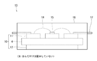
- FIG. 5 shows an example of a semiconductor module (semiconductor device) according to the embodiment.
- 10 is a ceramic circuit board
- 13 is a semiconductor module
- 14 is wire bonding
- 15 is a semiconductor element
- 16 is a resin mold
- 17 is a lead frame.
- the semiconductor element 15 is bonded to the metal circuit 11 of the ceramic circuit board 10 via a bonding layer (not shown).
- the lead frame 17 is joined via a joining layer (not shown).
- Adjacent metal circuits 11 are connected to each other by wire bonding 14.
- the wire bonding 14 and the metal circuit 11 are bonded.
- the ceramic circuit board 10 to which the wire bonding 14 is connected is integrated with the resin mold 16 to form the semiconductor module 13.
- the semiconductor module 13 is not limited to such a structure.
- the wire bonding 14 and the lead frame 17 may be either one.
- a plurality of semiconductor elements 15, wire bonding 14, and lead frames 17 may be provided in the metal circuit 11.
- examples of the joining layer for joining the semiconductor element 15 and the lead frame 17 include solder and a brazing material.
- Lead-free solder is preferable as the solder.
- the solder has a melting point of 450 [° C.] or less.
- the brazing material has a melting point of more than 450 [° C].
- a material having a melting point of 500 [° C.] or higher is called a high temperature brazing material.
- the high-temperature brazing material include those containing Ag as a main component.
- the screen surface is opposite to the metal circuit 11 (heat sink side) as in the ceramic circuit board 10 shown in FIG. This is because the non-continuous groove group 8 generated by the laser scribe is difficult for the resin to enter and may become a hole. Since the holes hinder the heat dissipation, the scribe line 3 is formed on the metal heat sink 12 side so as to suppress the generation.
- the semiconductor element 15 While the semiconductor element 15 is becoming smaller, the amount of heat generated from the chip is steadily increasing. Therefore, it is important to improve the heat dissipation in the ceramic circuit board 10 on which the semiconductor element 15 is mounted. Further, in order to improve the performance of the semiconductor module 13, a plurality of semiconductor elements 15 are mounted on the ceramic circuit board 10. If even one semiconductor element 15 exceeds the intrinsic temperature of the element, the resistance changes to the temperature coefficient on the negative negative side. Along with this, a phenomenon occurs in which a thermal runaway in which electric power flows intensively occurs and the electric power is instantly destroyed. Therefore, it is effective to improve the heat dissipation.
- the semiconductor device 13 can be used for a PCU, an IGBT, and an IPM module used for an inverter of an automobile (including an electric vehicle), an electric railway vehicle, an industrial machine, an air conditioner, and the like. Automobiles are becoming more and more electric vehicles. Improving the reliability of the semiconductor device 13 directly leads to the safety of the automobile. The same applies to electric railways and industrial equipment.
- the manufacturing method thereof is not particularly limited, but the following can be mentioned as a method for obtaining a good yield.
- the thermal conductivity of the silicon nitride substrate is 50 [W / m ⁇ K] or more and the three-point bending strength is 600 [MPa] or more. Is preferable.
- a silicon nitride substrate having a through hole is prepared.
- the through hole may be provided in advance at the stage of the molded body.
- a step of providing a through hole in the silicon nitride sintered body may be performed. The step of providing the through hole is performed by laser machining, cutting, or the like similar to laser scribe. Cutting is performed by drilling or the like with a drill or the like.
- the silicon nitride substrate is irradiated with a fiber laser to form a scribe line 3 composed of a continuous groove 7 and a discontinuous groove group 8.
- a continuous groove 7 and a discontinuous groove group 8 having a predetermined size are formed depending on the conditions of the fiber laser machine.
- the continuous groove 7 may be formed on the surface side by the fiber laser on the silicon nitride substrate as the ceramic scribe substrate 1, and then the discontinuous groove group 8 may be formed on the deep side by the fiber laser.
- one or a plurality of ceramic substrates 4 are manufactured by applying stress to the silicon nitride substrate as the ceramic scribe substrate 1 to divide the ceramic scribe substrate 1 along the scribe line 3.
- the metal circuit 11 is joined to the silicon nitride substrate as the ceramic substrate 4. It is preferable that the silicon nitride substrate and the metal circuit 11 are joined by an active metal joining method.
- the active metal joining method uses an active metal brazing material mixed with an active metal such as Ti.
- the active metal brazing material include a mixture of Ti, Ag, and Cu.
- Ti is 0.1 [wt%] or more and 10 [wt%] or less
- Cu is 10 [wt%] or more and 60 [wt%] or more.
- %] Ag is the balance.
- one or more selected from In, Sn, Al, Si, C, and Mg may be added in an amount of 1 [wt%] or more and 15 [wt%] or less.
- the active metal brazing material is made into a paste.
- the paste is a mixture of a brazing filler metal component and an organic substance, but the brazing filler metal component needs to be uniformly mixed. This is because if the brazing material components are unevenly distributed, the brazing is not stable and causes poor joining.
- the active metal brazing paste is applied to the ceramic substrate 4. Place a copper plate on it.
- a step of heating this at 600 [° C.] or more and 900 [° C.] or less to join is performed.
- the heating step shall be performed in vacuum or in a non-oxidizing atmosphere, if necessary. Further, when it is performed in a vacuum, it is preferably 1 ⁇ 10-2 [Pa] or less.
- the non-oxidizing atmosphere includes a nitrogen atmosphere and an argon atmosphere. Oxidation of the bonding layer can be suppressed by creating a vacuum or a non-oxidizing atmosphere. As a result, the joint strength can be improved.
- the metal circuit 11 to be joined may be either one processed into a pattern shape in advance for circuit formation or a single plate without pattern processing. When a single plate is used, it is processed into a pattern shape by etching after joining. At this time, the metal circuit 11 is formed on the surface opposite to the surface on which the scribe line 3 is formed. By this step, a silicon nitride metal circuit board as a ceramic circuit board 10 can be manufactured.
- a bonding layer is provided at a position where the semiconductor element 15 is bonded.
- the bonding layer is preferably solder or brazing material.
- a bonding layer is provided, and the semiconductor element 15 is provided on the bonding layer.
- the lead frame 17 is joined via the joining layer.
- wire bonding 14 shall be provided as needed.
- the semiconductor element 15, the lead frame 17, and the wire bonding 14 are provided with a necessary number. The inside is sealed by integrating the silicon nitride circuit board on which the semiconductor element 15, the lead frame 17, and the wire bonding 14 are performed with the resin mold 16.
- the ceramic circuit board 10 has been described as being manufactured by joining the metal circuit 11 or the like to the ceramic substrate 4 after being divided from the ceramic screen substrate 1, but the present invention is not limited to this case.
- a metal circuit 11 or the like is joined to the ceramic substrate 4 before division in the ceramic scribing substrate, and stress is applied to the ceramic scribing substrate 1 to which the metal circuit 11 or the like is bonded to divide the ceramic substrate 1 along the scribing line 3. (Results of Examples and Comparative Examples described later in Table 2). That is, the order of the division step of the ceramic scribe substrate 1 and the joining step of the metal circuit 11 or the like does not matter.
- the laser scribe method of the aluminum nitride substrate among the ceramic scribe substrate 1 according to the embodiment will be described.
- an aluminum nitride substrate is prepared.
- the thermal conductivity is 170 [W / m ⁇ K] or more and the three-point bending strength is 350 [MPa] or more.
- the manufacturing method of the laser screen of the aluminum nitride substrate is not particularly limited as long as it has the above-mentioned configuration, but as a method for obtaining a good yield, the above-mentioned silicon nitride substrate and silicon nitride circuit board are used. The same manufacturing process shall be taken.
- the ceramic screen substrate is a silicon nitride substrate (thermal conductivity 90 [W / m ⁇ K]) having a length of 40 [mm] ⁇ width of 50 [mm] and a thickness of 0.32 [mm] and 0.50 [mm].
- Three-point bending strength 650 [MPa] was prepared.
- an aluminum nitride substrate (thermal conductivity 170 [W / m ⁇ K], three-point bending) having a length of 40 [mm] ⁇ a width of 50 [mm] and a thickness of 0.635 [mm] and 0.80 [mm].
- Strength 400 [MPa] was prepared.
- an assist gas is used on the surface side of the ceramic scribe substrate by a fiber laser, and six lasers are used for one ceramic scribe substrate under each condition of Examples 1 to 32 and Comparative Examples 1 to 20. Processing was performed on 101 sheets at a time. One of the ceramic screen substrates after laser machining under each condition is divided, and the vicinity of the center of the cross section of the divided ceramic substrate (at a position of about 10 [mm] from the end) is multiplied by 100 by SEM. I observed it and took a picture. Lines were drawn on the surface of the ceramic substrate, the deepest part of the continuous groove, and the deepest part of the discontinuous groove group, and the depth D1 of the continuous groove and the depth D2 of the discontinuous groove group were obtained.
- the inter-groove distance P and the groove opening width W of the discontinuous groove group are arithmetically averaged by measuring the inter-groove distance P and the groove opening width W with the adjacent discontinuous groove group at 10 consecutive points in the photograph. I asked.
- Comparative Example 7 and Comparative Example 16 processing was performed without using the assist gas.
- Table 1 The measurement results of Examples and Comparative Examples are shown in Table 1 (in Table 1, the silicon nitride substrate is referred to as Si 3N 4 and the aluminum nitride substrate is referred to as Al N).
- the difference was obtained by measuring the brightness of the surface of the ceramic scribe substrate and the continuous groove, which were divided under each condition and observed by SEM photographs, with a microspectroscopic color difference meter.
- copper plates were joined to both sides by an active metal joining method.
- oxygen-free copper having a length of 40 [mm] ⁇ a width of 50 [mm] ⁇ a thickness of 0.5 [mm] was used.
- the active metal brazing material used in the active metal bonding method was made into a paste by mixing 2 [wt%] Ti, 10 [wt%] Sn, 30 [wt%] Cu, and Ag balance with an organic component. An active metal paste was used.
- a semi-automatic screen printing machine prints and dries the active metal paste on the scribing surface of the ceramic scribe substrate using a 320 x 320 [mm], 250 mesh, stainless V screen mesh, and subsequently prints and dries on the laser-non-irradiated surface. did. At this time, if the ceramic substrate was separated from the scribe line by pressurizing the squeegee of the printer, it was counted as a printing defect and was not distributed to the subsequent process.
- Copper plates were placed on both the upper and lower surfaces of the ceramic substrate on which the paste was printed and dried, and the paste was further sandwiched by a plate-shaped jig with a jig and a weight was placed from above to perform a heat bonding step.
- the heat bonding was performed in a vacuum (1 ⁇ 10-2 [Pa] or less) with a bonding temperature of 810 [° C.] and a bonding time of 10 minutes.
- the copper plate was etched to form a circuit shape.
- the front copper plate has three circuit shapes, and the back copper plate is also etched to provide a pullback around it.
- the etched ceramic substrate was scribed by an automatic substrate divider to obtain a ceramic circuit board. That is, a metal circuit or the like is joined to the ceramic substrate before division in the ceramic scribing substrate according to the examples and the comparative examples, and stress is applied to the ceramic scribing substrate to which the metal circuit or the like is bonded to divide the ceramic substrate along the scribing line. By doing so, a ceramic substrate circuit is manufactured. The appearance of the ceramic circuit board was inspected, and the cracks remaining, chips and cracks generated around the board were counted as scribe defects, and the products were not distributed in the subsequent process.
- a semiconductor element was mounted in the central circuit section of the ceramic circuit board manufactured from the ceramic screen substrate according to the examples and comparative examples. Next, wire bonding was performed. Then, it was integrated by a resin mold by a transfer molding method.
- the resin and the ceramic circuit board were subjected to the ultrasonic flaw detection method (SAT) around the substrate on the circuit side to which the semiconductor element was bonded.
- SAT ultrasonic flaw detection method
- the vacancy rate between them was evaluated.
- the porosity [%] is (total length of the portion where the resin does not adhere to the ceramic substrate and the pores exist / the peripheral length of the ceramic substrate) ⁇ 100, and a porosity of less than 95 [%] is defective in resin peeling. And said.
- Table 2 shows the results obtained for Examples and Comparative Examples.
- the scribe defect rate [%] and the resin peeling defect [%] were calculated as the defect rate per 100 product quantities, excluding the defects generated in the previous step.
- the defect rate was small as to whether or not the resin peeling defect occurred. Since there was no residue due to laser processing by laser scribe and no trace of continuous groove and discontinuous groove group at the resin molded part, unbonded due to laser residue and vacancies due to trace of continuous groove and discontinuous groove group occurred. Because it wasn't. On the other hand, in the ceramic circuit board manufactured from the ceramic scribe substrate according to the comparative example, many resin peeling defects occurred. This is because the unbonded due to the laser residue and the pores due to the continuous groove and the discontinuous groove group were peeled off and caused a defect.
Landscapes
- Chemical & Material Sciences (AREA)
- Engineering & Computer Science (AREA)
- Ceramic Engineering (AREA)
- Materials Engineering (AREA)
- Structural Engineering (AREA)
- Organic Chemistry (AREA)
- Manufacturing & Machinery (AREA)
- Microelectronics & Electronic Packaging (AREA)
- Physics & Mathematics (AREA)
- Optics & Photonics (AREA)
- Inorganic Chemistry (AREA)
- Structure Of Printed Boards (AREA)
- Laser Beam Processing (AREA)
- Manufacturing Of Printed Wiring (AREA)
Priority Applications (5)
| Application Number | Priority Date | Filing Date | Title |
|---|---|---|---|
| JP2022570023A JP7790836B2 (ja) | 2020-12-16 | 2021-12-14 | セラミックススクライブ基板、セラミックス基板、セラミックススクライブ基板の製造方法、セラミックス基板の製造方法、セラミックス回路基板の製造方法、及び、半導体素子の製造方法 |
| CN202180085324.8A CN116601761A (zh) | 2020-12-16 | 2021-12-14 | 陶瓷刻画基板、陶瓷基板、陶瓷刻画基板的制造方法、陶瓷基板的制造方法、陶瓷电路基板的制造方法、半导体元件的制造方法 |
| EP21906635.4A EP4266835B1 (en) | 2020-12-16 | 2021-12-14 | Ceramic scribe substrate, method for manufacturing ceramic scribe substrate, method for manufacturing ceramic substrate, method for manufacturing ceramic circuit board, and method for manufacturing semiconductor elements |
| US18/333,697 US20230326818A1 (en) | 2020-12-16 | 2023-06-13 | Ceramic scribe substrate, ceramic substrate, method for manufacturing ceramic scribe substrate, method for manufacturing ceramic substrate, method for manufacturing ceramic circuit board, and method for manufacturing semiconductor element |
| JP2024205375A JP2025027018A (ja) | 2020-12-16 | 2024-11-26 | セラミックススクライブ基板、セラミックス基板、セラミックススクライブ基板の製造方法、セラミックス基板の製造方法、セラミックス回路基板の製造方法、及び、半導体素子の製造方法 |
Applications Claiming Priority (2)
| Application Number | Priority Date | Filing Date | Title |
|---|---|---|---|
| JP2020-208106 | 2020-12-16 | ||
| JP2020208106 | 2020-12-16 |
Related Child Applications (1)
| Application Number | Title | Priority Date | Filing Date |
|---|---|---|---|
| US18/333,697 Continuation US20230326818A1 (en) | 2020-12-16 | 2023-06-13 | Ceramic scribe substrate, ceramic substrate, method for manufacturing ceramic scribe substrate, method for manufacturing ceramic substrate, method for manufacturing ceramic circuit board, and method for manufacturing semiconductor element |
Publications (1)
| Publication Number | Publication Date |
|---|---|
| WO2022131273A1 true WO2022131273A1 (ja) | 2022-06-23 |
Family
ID=82057833
Family Applications (1)
| Application Number | Title | Priority Date | Filing Date |
|---|---|---|---|
| PCT/JP2021/046148 Ceased WO2022131273A1 (ja) | 2020-12-16 | 2021-12-14 | セラミックススクライブ基板、セラミックス基板、セラミックススクライブ基板の製造方法、セラミックス基板の製造方法、セラミックス回路基板の製造方法、及び、半導体素子の製造方法 |
Country Status (5)
| Country | Link |
|---|---|
| US (1) | US20230326818A1 (https=) |
| EP (1) | EP4266835B1 (https=) |
| JP (2) | JP7790836B2 (https=) |
| CN (1) | CN116601761A (https=) |
| WO (1) | WO2022131273A1 (https=) |
Cited By (1)
| Publication number | Priority date | Publication date | Assignee | Title |
|---|---|---|---|---|
| JP2025027018A (ja) * | 2020-12-16 | 2025-02-26 | 株式会社東芝 | セラミックススクライブ基板、セラミックス基板、セラミックススクライブ基板の製造方法、セラミックス基板の製造方法、セラミックス回路基板の製造方法、及び、半導体素子の製造方法 |
Families Citing this family (1)
| Publication number | Priority date | Publication date | Assignee | Title |
|---|---|---|---|---|
| US20230307314A1 (en) * | 2022-03-24 | 2023-09-28 | Texas Instruments Incorporated | Direct bond copper substrate with metal filled ceramic substrate indentations |
Citations (8)
| Publication number | Priority date | Publication date | Assignee | Title |
|---|---|---|---|---|
| JPS62174364U (https=) * | 1986-04-25 | 1987-11-05 | ||
| JP2001267458A (ja) * | 2000-03-22 | 2001-09-28 | New Japan Radio Co Ltd | セラミック集合基板、これを用いた半導体装置及びその製造方法 |
| JP2002076532A (ja) * | 2000-08-28 | 2002-03-15 | Kyocera Corp | セラミック回路基板 |
| JP2002176119A (ja) | 2000-12-06 | 2002-06-21 | Toshiba Corp | 窒化珪素基板およびそれを用いた窒化珪素回路基板並びにその製造方法 |
| JP2006036602A (ja) * | 2004-07-28 | 2006-02-09 | Kyocera Corp | セラミック部材およびその製造方法、ならびにこれを用いた電子部品 |
| WO2009154295A1 (ja) * | 2008-06-20 | 2009-12-23 | 日立金属株式会社 | セラミックス集合基板とその製造方法及びセラミックス基板並びにセラミックス回路基板 |
| JP2011071374A (ja) * | 2009-09-28 | 2011-04-07 | Kyocera Corp | 多数個取り配線基板およびその製造方法 |
| JP6399252B2 (ja) | 2016-03-28 | 2018-10-03 | 日立金属株式会社 | 回路基板および窒化ケイ素焼結基板の製造方法 |
Family Cites Families (6)
| Publication number | Priority date | Publication date | Assignee | Title |
|---|---|---|---|---|
| CN101849445B (zh) * | 2007-11-06 | 2012-11-21 | 三菱综合材料株式会社 | 陶瓷基板、陶瓷基板的制造方法和电源模块用基板的制造方法 |
| JP6642146B2 (ja) * | 2015-03-31 | 2020-02-05 | 日立金属株式会社 | 窒化珪素系セラミックス集合基板及びその製造方法 |
| JP7741725B2 (ja) * | 2019-03-01 | 2025-09-18 | デンカ株式会社 | セラミックグリーンシート、セラミック基板、セラミックグリーンシートの製造方法およびセラミック基板の製造方法 |
| JP7606449B2 (ja) * | 2019-03-15 | 2024-12-25 | デンカ株式会社 | 窒化ケイ素基板の製造方法及び窒化ケイ素基材 |
| CN113597674B (zh) | 2019-04-11 | 2025-01-17 | 株式会社东芝 | 陶瓷铜电路基板及使用了其的半导体装置 |
| EP4266835B1 (en) * | 2020-12-16 | 2026-04-29 | Niterra Materials Co., Ltd. | Ceramic scribe substrate, method for manufacturing ceramic scribe substrate, method for manufacturing ceramic substrate, method for manufacturing ceramic circuit board, and method for manufacturing semiconductor elements |
-
2021
- 2021-12-14 EP EP21906635.4A patent/EP4266835B1/en active Active
- 2021-12-14 CN CN202180085324.8A patent/CN116601761A/zh active Pending
- 2021-12-14 JP JP2022570023A patent/JP7790836B2/ja active Active
- 2021-12-14 WO PCT/JP2021/046148 patent/WO2022131273A1/ja not_active Ceased
-
2023
- 2023-06-13 US US18/333,697 patent/US20230326818A1/en active Pending
-
2024
- 2024-11-26 JP JP2024205375A patent/JP2025027018A/ja active Pending
Patent Citations (8)
| Publication number | Priority date | Publication date | Assignee | Title |
|---|---|---|---|---|
| JPS62174364U (https=) * | 1986-04-25 | 1987-11-05 | ||
| JP2001267458A (ja) * | 2000-03-22 | 2001-09-28 | New Japan Radio Co Ltd | セラミック集合基板、これを用いた半導体装置及びその製造方法 |
| JP2002076532A (ja) * | 2000-08-28 | 2002-03-15 | Kyocera Corp | セラミック回路基板 |
| JP2002176119A (ja) | 2000-12-06 | 2002-06-21 | Toshiba Corp | 窒化珪素基板およびそれを用いた窒化珪素回路基板並びにその製造方法 |
| JP2006036602A (ja) * | 2004-07-28 | 2006-02-09 | Kyocera Corp | セラミック部材およびその製造方法、ならびにこれを用いた電子部品 |
| WO2009154295A1 (ja) * | 2008-06-20 | 2009-12-23 | 日立金属株式会社 | セラミックス集合基板とその製造方法及びセラミックス基板並びにセラミックス回路基板 |
| JP2011071374A (ja) * | 2009-09-28 | 2011-04-07 | Kyocera Corp | 多数個取り配線基板およびその製造方法 |
| JP6399252B2 (ja) | 2016-03-28 | 2018-10-03 | 日立金属株式会社 | 回路基板および窒化ケイ素焼結基板の製造方法 |
Non-Patent Citations (1)
| Title |
|---|
| See also references of EP4266835A4 |
Cited By (1)
| Publication number | Priority date | Publication date | Assignee | Title |
|---|---|---|---|---|
| JP2025027018A (ja) * | 2020-12-16 | 2025-02-26 | 株式会社東芝 | セラミックススクライブ基板、セラミックス基板、セラミックススクライブ基板の製造方法、セラミックス基板の製造方法、セラミックス回路基板の製造方法、及び、半導体素子の製造方法 |
Also Published As
| Publication number | Publication date |
|---|---|
| CN116601761A (zh) | 2023-08-15 |
| JPWO2022131273A1 (https=) | 2022-06-23 |
| JP2025027018A (ja) | 2025-02-26 |
| US20230326818A1 (en) | 2023-10-12 |
| JP7790836B2 (ja) | 2025-12-23 |
| EP4266835A4 (en) | 2024-12-04 |
| EP4266835B1 (en) | 2026-04-29 |
| EP4266835A1 (en) | 2023-10-25 |
Similar Documents
| Publication | Publication Date | Title |
|---|---|---|
| US9968012B2 (en) | Heat-sink-attached power module substrate, heat-sink-attached power module, and method for producing heat-sink-attached power module substrate | |
| JP2025027018A (ja) | セラミックススクライブ基板、セラミックス基板、セラミックススクライブ基板の製造方法、セラミックス基板の製造方法、セラミックス回路基板の製造方法、及び、半導体素子の製造方法 | |
| KR20200004799A (ko) | 세라믹스 회로 기판 및 그 제조 방법과 그것을 사용한 모듈 | |
| KR20200013678A (ko) | 세라믹스 회로 기판 및 그것을 사용한 모듈 | |
| JPWO2018180965A1 (ja) | セラミックス銅回路基板およびそれを用いた半導体装置 | |
| WO2003090277A1 (fr) | Carte de circuits imprimes, son procede de production et module de puissance | |
| CN101529588A (zh) | 功率模块用基板以及功率模块用基板的制造方法、及功率模块 | |
| JP2025038181A (ja) | セラミックス銅回路基板、半導体装置、セラミックス銅回路基板の製造方法、及び半導体装置の製造方法 | |
| WO2020105734A1 (ja) | セラミックス-銅複合体、セラミックス-銅複合体の製造方法、セラミックス回路基板およびパワーモジュール | |
| JP6020256B2 (ja) | ヒートシンク付パワーモジュール用基板の製造方法 | |
| JP7281603B2 (ja) | 複合基板 | |
| US20240332123A1 (en) | Scribed ceramic circuit substrate, ceramic circuit substrate, method for producing scribed ceramic circuit substrate, method for producing ceramic circuit substrate, and method for producing semiconductor device | |
| JP2005235968A (ja) | 接着性高熱伝導樹脂シートおよびそれを用いた電子機器装置 | |
| JP3779074B2 (ja) | セラミックス回路基板とそれを用いたパワーモジュール | |
| JP4935753B2 (ja) | パワーモジュール用基板、パワーモジュール及びパワーモジュール用基板の製造方法 | |
| JP2013214541A (ja) | パワーモジュール用基板の製造方法及びパワーモジュール用基板 | |
| JPWO2023120654A5 (https=) | ||
| CN111819681B (zh) | 带散热器的绝缘电路基板 | |
| JP5039070B2 (ja) | 半導体装置 | |
| JP7330382B2 (ja) | 複合基板 | |
| JP6422294B2 (ja) | 電子モジュール用基板の製造方法及び電子モジュール用基板 | |
| JP2025168438A (ja) | スクレイパー及びそれを用いたスクリーン印刷機、ならびに該スクレイパーを用いたセラミックス回路基板及び半導体装置の製造方法 | |
| WO2025013789A1 (ja) | セラミックス回路基板およびその製造方法 | |
| WO2023204054A1 (ja) | セラミックス回路基板、半導体装置、セラミックス回路基板の製造方法、及び半導体装置の製造方法 | |
| WO2025063256A1 (ja) | セラミックススクライブ基板、セラミックススクライブ基板の製造方法、セラミックス基板の製造方法、及び、セラミックス回路基板の製造方法 |
Legal Events
| Date | Code | Title | Description |
|---|---|---|---|
| 121 | Ep: the epo has been informed by wipo that ep was designated in this application |
Ref document number: 21906635 Country of ref document: EP Kind code of ref document: A1 |
|
| ENP | Entry into the national phase |
Ref document number: 2022570023 Country of ref document: JP Kind code of ref document: A |
|
| WWE | Wipo information: entry into national phase |
Ref document number: 202180085324.8 Country of ref document: CN |
|
| NENP | Non-entry into the national phase |
Ref country code: DE |
|
| ENP | Entry into the national phase |
Ref document number: 2021906635 Country of ref document: EP Effective date: 20230717 |