WO2022130835A1 - 撮像装置 - Google Patents
撮像装置 Download PDFInfo
- Publication number
- WO2022130835A1 WO2022130835A1 PCT/JP2021/041249 JP2021041249W WO2022130835A1 WO 2022130835 A1 WO2022130835 A1 WO 2022130835A1 JP 2021041249 W JP2021041249 W JP 2021041249W WO 2022130835 A1 WO2022130835 A1 WO 2022130835A1
- Authority
- WO
- WIPO (PCT)
- Prior art keywords
- electrode
- control electrode
- voltage
- pixel electrode
- photoelectric conversion
- Prior art date
Links
- 238000006243 chemical reaction Methods 0.000 claims abstract description 105
- 230000035945 sensitivity Effects 0.000 claims description 159
- 238000003384 imaging method Methods 0.000 claims description 14
- 239000011368 organic material Substances 0.000 claims description 3
- 239000010410 layer Substances 0.000 description 74
- 230000004048 modification Effects 0.000 description 36
- 238000012986 modification Methods 0.000 description 36
- 230000003321 amplification Effects 0.000 description 23
- 238000003199 nucleic acid amplification method Methods 0.000 description 23
- 238000010586 diagram Methods 0.000 description 18
- 239000004065 semiconductor Substances 0.000 description 18
- 239000000758 substrate Substances 0.000 description 18
- 239000012535 impurity Substances 0.000 description 12
- 239000011229 interlayer Substances 0.000 description 11
- 238000009825 accumulation Methods 0.000 description 8
- 230000000875 corresponding effect Effects 0.000 description 8
- 230000000694 effects Effects 0.000 description 7
- 229920006395 saturated elastomer Polymers 0.000 description 7
- 230000001276 controlling effect Effects 0.000 description 6
- 238000001514 detection method Methods 0.000 description 5
- 238000009413 insulation Methods 0.000 description 5
- 238000000034 method Methods 0.000 description 5
- 230000002093 peripheral effect Effects 0.000 description 5
- 238000007789 sealing Methods 0.000 description 4
- XUIMIQQOPSSXEZ-UHFFFAOYSA-N Silicon Chemical compound [Si] XUIMIQQOPSSXEZ-UHFFFAOYSA-N 0.000 description 3
- 238000000926 separation method Methods 0.000 description 3
- 229910052710 silicon Inorganic materials 0.000 description 3
- 239000010703 silicon Substances 0.000 description 3
- RYGMFSIKBFXOCR-UHFFFAOYSA-N Copper Chemical compound [Cu] RYGMFSIKBFXOCR-UHFFFAOYSA-N 0.000 description 2
- 229910052782 aluminium Inorganic materials 0.000 description 2
- XAGFODPZIPBFFR-UHFFFAOYSA-N aluminium Chemical compound [Al] XAGFODPZIPBFFR-UHFFFAOYSA-N 0.000 description 2
- 239000003990 capacitor Substances 0.000 description 2
- 229910052802 copper Inorganic materials 0.000 description 2
- 239000010949 copper Substances 0.000 description 2
- 229910052751 metal Inorganic materials 0.000 description 2
- 239000002184 metal Substances 0.000 description 2
- 230000000737 periodic effect Effects 0.000 description 2
- 229910021420 polycrystalline silicon Inorganic materials 0.000 description 2
- 229920005591 polysilicon Polymers 0.000 description 2
- 238000009751 slip forming Methods 0.000 description 2
- 101100041125 Arabidopsis thaliana RST1 gene Proteins 0.000 description 1
- 101100443250 Saccharomyces cerevisiae (strain ATCC 204508 / S288c) DIG1 gene Proteins 0.000 description 1
- 101100443251 Saccharomyces cerevisiae (strain ATCC 204508 / S288c) DIG2 gene Proteins 0.000 description 1
- 101100041128 Schizosaccharomyces pombe (strain 972 / ATCC 24843) rst2 gene Proteins 0.000 description 1
- 229910021417 amorphous silicon Inorganic materials 0.000 description 1
- 230000000903 blocking effect Effects 0.000 description 1
- 239000003086 colorant Substances 0.000 description 1
- 230000002596 correlated effect Effects 0.000 description 1
- 230000007423 decrease Effects 0.000 description 1
- 230000005684 electric field Effects 0.000 description 1
- 238000004519 manufacturing process Methods 0.000 description 1
- 239000000463 material Substances 0.000 description 1
- 230000003071 parasitic effect Effects 0.000 description 1
- 238000005070 sampling Methods 0.000 description 1
- 230000001629 suppression Effects 0.000 description 1
- 239000012780 transparent material Substances 0.000 description 1
Images


Classifications
-
- H—ELECTRICITY
- H01—ELECTRIC ELEMENTS
- H01L—SEMICONDUCTOR DEVICES NOT COVERED BY CLASS H10
- H01L27/00—Devices consisting of a plurality of semiconductor or other solid-state components formed in or on a common substrate
- H01L27/14—Devices consisting of a plurality of semiconductor or other solid-state components formed in or on a common substrate including semiconductor components sensitive to infrared radiation, light, electromagnetic radiation of shorter wavelength or corpuscular radiation and specially adapted either for the conversion of the energy of such radiation into electrical energy or for the control of electrical energy by such radiation
- H01L27/144—Devices controlled by radiation
- H01L27/146—Imager structures
- H01L27/14601—Structural or functional details thereof
- H01L27/14603—Special geometry or disposition of pixel-elements, address-lines or gate-electrodes
-
- H—ELECTRICITY
- H01—ELECTRIC ELEMENTS
- H01L—SEMICONDUCTOR DEVICES NOT COVERED BY CLASS H10
- H01L27/00—Devices consisting of a plurality of semiconductor or other solid-state components formed in or on a common substrate
- H01L27/14—Devices consisting of a plurality of semiconductor or other solid-state components formed in or on a common substrate including semiconductor components sensitive to infrared radiation, light, electromagnetic radiation of shorter wavelength or corpuscular radiation and specially adapted either for the conversion of the energy of such radiation into electrical energy or for the control of electrical energy by such radiation
- H01L27/144—Devices controlled by radiation
- H01L27/146—Imager structures
- H01L27/14643—Photodiode arrays; MOS imagers
- H01L27/14645—Colour imagers
-
- H—ELECTRICITY
- H04—ELECTRIC COMMUNICATION TECHNIQUE
- H04N—PICTORIAL COMMUNICATION, e.g. TELEVISION
- H04N25/00—Circuitry of solid-state image sensors [SSIS]; Control thereof
- H04N25/70—SSIS architectures; Circuits associated therewith
- H04N25/709—Circuitry for control of the power supply
-
- H—ELECTRICITY
- H04—ELECTRIC COMMUNICATION TECHNIQUE
- H04N—PICTORIAL COMMUNICATION, e.g. TELEVISION
- H04N25/00—Circuitry of solid-state image sensors [SSIS]; Control thereof
- H04N25/70—SSIS architectures; Circuits associated therewith
- H04N25/76—Addressed sensors, e.g. MOS or CMOS sensors
-
- H—ELECTRICITY
- H04—ELECTRIC COMMUNICATION TECHNIQUE
- H04N—PICTORIAL COMMUNICATION, e.g. TELEVISION
- H04N25/00—Circuitry of solid-state image sensors [SSIS]; Control thereof
- H04N25/70—SSIS architectures; Circuits associated therewith
- H04N25/76—Addressed sensors, e.g. MOS or CMOS sensors
- H04N25/77—Pixel circuitry, e.g. memories, A/D converters, pixel amplifiers, shared circuits or shared components
Definitions
- This disclosure relates to an image pickup device.
- Patent Document 1 and Patent Document 2 disclose a stacked image pickup device having variable sensitivity.
- the present disclosure provides an imaging device capable of changing the sensitivity in a wide range.
- the image pickup apparatus has a first surface and a second surface facing the first surface, and is on a photoelectric conversion layer that generates a signal charge and the first surface of the photoelectric conversion layer. At least one pixel electrode located, a control electrode located on the first surface of the photoelectric conversion layer and for controlling the sensitivity of the image pickup device, and a control electrode located on the second surface of the photoelectric conversion layer. A counter electrode facing the at least one pixel electrode and the control electrode, and a charge storage unit connected to the at least one pixel electrode and accumulating the signal charge. There is a line segment connecting two points on the at least one pixel electrode and overlapping with the control electrode in a plan view.
- the sensitivity can be changed in a wide range.
- FIG. 1 is a diagram schematically showing an example of a circuit configuration of the image pickup apparatus according to the first embodiment.
- FIG. 2 is a cross-sectional view schematically showing a device structure of a unit pixel cell of the image pickup apparatus according to the first embodiment.
- FIG. 3 is a plan view showing a pixel electrode and a control electrode of the image pickup apparatus according to the first embodiment.
- FIG. 4A is a schematic cross-sectional view showing an example of a region formed in the photoelectric conversion layer when a voltage is applied to the control electrode and in which a signal charge that can move to the pixel electrode exists.
- FIG. 4B is a schematic plan view showing an example of a region formed in the photoelectric conversion layer when a voltage is applied to the control electrode and in which a signal charge that can move to the pixel electrode exists.
- FIG. 4C is a schematic cross-sectional view showing an example of a region formed in the photoelectric conversion layer when a voltage is applied to the control electrode and in which a signal charge that can move to the pixel electrode exists.
- FIG. 4D is a schematic plan view showing an example of a region formed in the photoelectric conversion layer when a voltage is applied to the control electrode and in which a signal charge that can move to the pixel electrode exists.
- FIG. 5 is a diagram showing an example of a circuit configuration of a unit pixel cell of the image pickup apparatus according to the first embodiment.
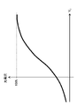
- FIG. 6 is a diagram showing an example of the relationship between the potential difference between the electrodes of the image pickup apparatus according to the first embodiment and the photocurrent.
- FIG. 7 is a diagram showing an example of the relationship between the voltage applied to the control electrode and the photocurrent in the image pickup apparatus according to the first embodiment.
- FIG. 8 is a diagram showing a first modification example of the shapes of the control electrode and the pixel electrode of the image pickup apparatus according to the first embodiment.
- FIG. 9 is a diagram showing a second modification example of the shapes of the control electrode and the pixel electrode of the image pickup apparatus according to the first embodiment.
- FIG. 10 is a diagram showing a third modification example of the shapes of the control electrode and the pixel electrode of the image pickup apparatus according to the first embodiment.
- FIG. 11 is a diagram showing a fourth modification example of the shapes of the control electrode and the pixel electrode of the image pickup apparatus according to the first embodiment.
- FIG. 12 is a diagram showing a fifth modification example of the shapes of the control electrode and the pixel electrode of the image pickup apparatus according to the first embodiment.
- FIG. 13 is a timing chart showing an example of the operation of the image pickup apparatus according to the first embodiment.
- FIG. 14 is a timing chart showing another example of the operation of the image pickup apparatus according to the first embodiment.
- FIG. 15 is a timing chart showing still another example of the operation of the image pickup apparatus according to the first embodiment.
- FIG. 16 is a timing chart showing still another example of the operation of the image pickup apparatus according to the first embodiment.
- Patent Document 1 changes the sensitivity by changing the voltage of the counter electrode.
- the sensitivity to the voltage of the counter electrode cannot be kept constant. That is, even if the potential of the counter electrode is set to a certain value, the sensitivity changes due to the accumulation of signal charges.
- Patent Document 2 changes the sensitivity by arranging a shield electrode around the pixel electrode and changing the voltage applied to the shield electrode.
- the shield electrodes are arranged between the pixels, it is difficult to change the sensitivity in a wide range even if the voltage applied to the shield electrodes is changed.
- the inventors have focused on the shapes and arrangements of the pixel electrodes and shield electrodes, and have reached the present disclosure.
- the pixel electrodes and control electrodes are shaped and arranged so as to satisfy predetermined conditions, so that the sensitivity can be changed in a wide range while keeping the sensitivity substantially constant with respect to the applied voltage.
- An image pickup device is provided.
- the image pickup apparatus has a first surface and a second surface facing the first surface, and has a photoelectric conversion layer that generates a signal charge and the first surface of the photoelectric conversion layer. At least one pixel electrode located in, a control electrode located on the first surface of the photoelectric conversion layer and for controlling the sensitivity of the image pickup device, and a control electrode located on the second surface of the photoelectric conversion layer. A counter electrode facing the at least one pixel electrode and the control electrode, and a charge storage unit connected to the at least one pixel electrode and accumulating the signal charge are provided. There is a line segment connecting two points on the at least one pixel electrode and overlapping with the control electrode in a plan view.
- control electrode may be surrounded by the at least one pixel electrode.
- control electrode may overlap with the center of the smallest circle completely including the at least one pixel electrode.
- the image pickup device may further include a microlens located above the second surface.
- control electrode may overlap with a point where the thickness of the microlens is maximized.
- the incident light can be focused on the region affected by the voltage applied to the control electrode. Therefore, the sensitivity can be changed in a wider range.
- the photoelectric conversion layer may contain an organic material.
- the image pickup apparatus may further include at least one pixel electrode and a shield electrode surrounding the control electrode in a plan view, which is located on the first surface.
- control electrode may be electrically connected to the shield electrode.
- the voltage of the shield electrode and the voltage of the control electrode are shared, so the number of power supplies can be reduced.
- the image pickup apparatus further includes a voltage supply circuit, the signal charge is a hole, the voltage supply circuit supplies a first voltage to the counter electrode, and the first voltage is supplied to the control electrode.
- the following second voltage may be supplied.
- the amount of signal charge collected in the pixel electrode can be controlled by the voltage applied to the control electrode. That is, the sensitivity can be changed by the voltage applied to the control electrode.
- the voltage supply circuit supplies the second voltage to the control electrode in the first frame period, and supplies a third voltage lower than the second voltage in the second frame period different from the first frame period. May be supplied.
- the image pickup apparatus has a first surface and a second surface facing the first surface, and has a photoelectric conversion layer that generates a signal charge and the first surface of the photoelectric conversion layer. At least one pixel electrode located in, a control electrode located on the first surface of the photoelectric conversion layer and for controlling the sensitivity of the image pickup device, and a control electrode located on the second surface of the photoelectric conversion layer. A counter electrode facing the at least one pixel electrode and the control electrode, and a charge storage unit connected to the at least one pixel electrode and accumulating the signal charge are provided. In plan view, the control electrode overlaps the center of the smallest circle that completely contains the at least one pixel electrode.
- the image pickup apparatus has a first surface and a second surface facing the first surface, and has a photoelectric conversion layer that generates a signal charge and the first surface of the photoelectric conversion layer.
- the signal charge is connected to the at least one pixel electrode, the counter electrode facing the control electrode, the microlens located above the second surface of the photoelectric conversion layer, and the at least one pixel electrode. It is provided with a charge storage unit for accumulating.
- the control electrode overlaps with the point where the thickness of the microlens is maximized.
- each figure is a schematic diagram and is not necessarily exactly illustrated. Therefore, for example, the scales and the like do not always match in each figure.
- planar view means a view from a direction perpendicular to the semiconductor substrate.
- FIG. 1 schematically shows an example of the circuit configuration of the image pickup apparatus 101 according to the first embodiment.
- the image pickup apparatus 101 includes a plurality of unit pixel cells 14 and a peripheral circuit.
- the plurality of unit pixel cells 14 are arranged two-dimensionally on the semiconductor substrate, that is, in the row direction and the column direction to form a photosensitive region (pixel region).
- the image pickup apparatus 101 may be a line sensor, and the plurality of unit pixel cells 14 may be arranged one-dimensionally.
- the row and column directions refer to the directions in which the rows and columns extend, respectively. That is, in FIG. 1, the vertical direction is the column direction and the horizontal direction is the row direction.
- Each unit pixel cell 14 includes a photoelectric conversion unit 10, an amplification transistor 11, a reset transistor 12, and an address transistor 13.
- the photoelectric conversion unit 10 includes a pixel electrode 50, a control electrode 61, and a counter electrode 52. By adjusting the voltage applied to the control electrode 61, the amount of the signal charge generated by the photoelectric conversion captured by the pixel electrode 50 is adjusted. That is, the sensitivity of the image pickup apparatus 101 is adjusted.
- the image pickup apparatus 101 has a voltage application circuit 60 as an example of a voltage supply circuit.
- the voltage application circuit 60 is configured to be able to simultaneously or selectively apply at least two different voltages to the control electrode 61 during the operation of the image pickup apparatus 101.
- the voltage application circuit 60 may have a configuration capable of changing the voltage supplied to the control electrode 61.
- the circuit configuration of the voltage application circuit 60 is not limited to a specific circuit configuration.
- the voltage application circuit 60 may have a configuration for converting a voltage supplied from a voltage source into a predetermined voltage.
- the voltage application circuit 60 itself may be configured to generate a predetermined voltage.
- the voltage supplied from the voltage application circuit 60 to the control electrode 61 is referred to as a sensitivity adjustment voltage Vc.
- the voltage application circuit 60 sets the sensitivity adjustment voltage Vc according to the command of the operator who operates the image pickup device 101 or the command of another control circuit included in the image pickup device 101 via the sensitivity adjustment line 28, via the control electrode. Supply to 61.
- the voltage application circuit 60 is typically provided outside the photosensitive region as part of a peripheral circuit.
- the sensitivity adjustment line 28 is provided for each line in FIG. 1, but is not limited to this.
- the sensitivity adjustment line 28 may be common to all pixels or may be provided for each pixel. Further, when the sensitivity adjustment line 28 is provided for each row, the sensitivity adjustment voltage Vc may be changed individually for each row or may be changed simultaneously for all the rows.
- the pixel electrode 50 is connected to the gate electrode of the amplification transistor 11.
- the signal charge collected by the pixel electrode 50 is stored in the charge storage node 24 located between the pixel electrode 50 and the gate electrode of the amplification transistor 11.
- the signal charge is a hole, but the signal charge may be an electron.
- the signal charge stored in the charge storage node 24 is applied to the gate electrode of the amplification transistor 11 as a voltage corresponding to the amount of the signal charge.
- the amplification transistor 11 amplifies this voltage.
- the signal voltage is selectively read by the address transistor 13.
- the source or drain electrode of the reset transistor 12 is connected to the pixel electrode 50.
- the reset transistor 12 resets the signal charge stored in the charge storage node 24. In other words, the reset transistor 12 resets the potentials of the gate electrode and the pixel electrode 50 of the amplification transistor 11.
- the image pickup apparatus 101 includes a power supply wiring 21, a vertical signal line 17, an address signal line 26, and a reset signal line 27. These lines are connected to the unit pixel cell 14, respectively.
- the power supply wiring 21 is connected to the source or drain electrode of the amplification transistor 11.
- the vertical signal line 17 is connected to the source or drain electrode of the address transistor 13.
- the address signal line 26 is connected to the gate electrode of the address transistor 13.
- the reset signal line 27 is connected to the gate electrode of the reset transistor 12.
- the image pickup apparatus 101 includes a photoelectric conversion unit control line 16 for applying a predetermined voltage to the photoelectric conversion unit 10.
- the voltage supplied to the photoelectric conversion unit 10 via the photoelectric conversion unit control line 16 may be common to all the photoelectric conversion units 10.
- the voltage supplied to the photoelectric conversion unit 10 via the photoelectric conversion unit control line 16 may be a voltage having a constant magnitude or a voltage that changes with time.
- the peripheral circuit includes a vertical scanning circuit 15, a horizontal signal reading circuit 20, a plurality of column signal processing circuits 19, a plurality of load circuits 18, and a plurality of inverting amplifiers 22.
- the vertical scanning circuit 15 is also referred to as a row scanning circuit.
- the horizontal signal reading circuit 20 is also referred to as a column scanning circuit.
- the column signal processing circuit 19 is also referred to as a row signal storage circuit.
- the inverting amplifier 22 is also referred to as a feedback amplifier.
- the vertical scanning circuit 15 is connected to the address signal line 26 and the reset signal line 27.
- the vertical scanning circuit 15 selects a plurality of unit pixel cells 14 arranged in each row in row units, reads out a signal voltage, and resets the potential of the pixel electrode 50.
- the power supply wiring 21 supplies a predetermined power supply voltage to the amplification transistor 11 of each unit pixel cell 14.
- the horizontal signal reading circuit 20 is electrically connected to a plurality of column signal processing circuits 19.
- the column signal processing circuit 19 is electrically connected to the unit pixel cell 14 arranged in each row via the vertical signal line 17 corresponding to each row.
- the load circuit 18 is electrically connected to each vertical signal line 17.
- the load circuit 18 and the amplification transistor 11 form a source follower circuit.
- a plurality of inverting amplifiers 22 are provided corresponding to each row.
- the negative input terminal of the inverting amplifier 22 is connected to the corresponding vertical signal line 17. Further, the output terminal of the inverting amplifier 22 is connected to the unit pixel cell 14 via the feedback line 23 corresponding to each row.
- the vertical scanning circuit 15 applies a row selection signal for controlling the on / off of the address transistor 13 to the gate electrode of the address transistor 13 by the address signal line 26. As a result, the row to be read is scanned and selected. A signal voltage is read from the unit pixel cell 14 in the selected row to the vertical signal line 17. Further, the vertical scanning circuit 15 applies a reset signal for controlling on and off of the reset transistor 12 to the gate electrode of the reset transistor 12 via the reset signal line 27. As a result, the row of the unit pixel cell 14 that is the target of the reset operation is selected. The vertical signal line 17 transmits the signal voltage read from the unit pixel cell 14 selected by the vertical scanning circuit 15 to the column signal processing circuit 19.
- the column signal processing circuit 19 performs noise suppression signal processing represented by correlated double sampling and analog-to-digital conversion (AD conversion), for example.
- the horizontal signal reading circuit 20 sequentially reads signals from the plurality of column signal processing circuits 19 to the horizontal common signal line 29.
- the inverting amplifier 22 is connected to the drain electrode of the reset transistor 12 via the feedback line 23. Therefore, the inverting amplifier 22 receives the output of the address transistor 13 at the negative terminal when the address transistor 13 and the reset transistor 12 are in a conducting state.
- the inverting amplifier 22 performs a feedback operation so that the gate potential of the amplification transistor 11 becomes a predetermined feedback voltage. At this time, the output voltage value of the inverting amplifier 22 is 0V or a positive voltage in the vicinity of 0V.
- the feedback voltage means the output voltage of the inverting amplifier 22.
- FIG. 2 is a cross-sectional view schematically showing a cross section of the device structure of the unit pixel cell 14 in the image pickup apparatus 101 according to the present embodiment.
- the unit pixel cell 14 includes a semiconductor substrate 31, a charge detection circuit 25, a photoelectric conversion unit 10, a sealing film 53, a color filter 54, and a microlens 55.
- the semiconductor substrate 31 is, for example, a p-type silicon substrate.
- the charge detection circuit 25 detects the signal charge captured by the pixel electrode 50 and outputs the signal voltage.
- the charge detection circuit 25 includes an amplification transistor 11, a reset transistor 12, and an address transistor 13, and is formed on the semiconductor substrate 31.
- the amplification transistor 11 is formed on the semiconductor substrate 31, and has n-type impurity regions 41C and 41D that function as drains and sources, respectively, a gate insulating layer 38B located on the semiconductor substrate 31, and a gate located on the gate insulating layer 38B. Includes electrode 39B.
- the reset transistor 12 is formed on the semiconductor substrate 31, and has n-type impurity regions 41B and 41A that function as drains and sources, respectively, a gate insulating layer 38A located on the semiconductor substrate 31, and a gate located on the gate insulating layer 38A. Includes electrode 39A.
- the address transistor 13 is formed on the semiconductor substrate 31, and has n-type impurity regions 41D and 41E that function as drains and sources, respectively, and a gate insulating layer 38C located on the semiconductor substrate 31 and a gate electrode located on the gate insulating layer 38C. Including 39C.
- the n-type impurity region 41D is shared by the amplification transistor 11 and the address transistor 13, whereby the amplification transistor 11 and the address transistor 13 are connected in series.
- an element separation region 42 is provided between the adjacent unit pixel cells 14 and between the amplification transistor 11 and the reset transistor 12.
- the element separation region 42 electrically separates the adjacent unit pixel cells 14. Further, the leakage of the signal charge accumulated in the charge storage node 24 is suppressed.
- Interlayer insulation layers 43A, 43B and 43C are laminated on the surface of the semiconductor substrate 31.
- a contact plug 45A and a contact plug 45B are contained in the interlayer insulating layer 43A.
- the wiring 46A to be connected is provided in the interlayer insulating layer 43A.
- the n-type impurity region 41B as the drain of the reset transistor 12 is electrically connected to the gate electrode 39B of the amplification transistor 11.
- the photoelectric conversion unit 10 is provided on the interlayer insulating layer 43C.
- the photoelectric conversion unit 10 includes a counter electrode 52, a photoelectric conversion layer 51, a pixel electrode 50, and a control electrode 61.
- the photoelectric conversion layer 51 is sandwiched between the counter electrode 52, the pixel electrode 50, and the control electrode 61.
- the pixel electrode 50 and the control electrode 61 are provided on the interlayer insulating layer 43C.
- the counter electrode 52 is formed of a conductive transparent material such as ITO.
- the pixel electrode 50 and the control electrode 61 are formed of, for example, aluminum, a metal containing copper, or polysilicon doped with impurities to impart conductivity.
- the sealing film 53 is an insulating film provided on the counter electrode 52.
- the color filter 54 is provided on the sealing film 53 and selectively passes light in a specific wavelength range.
- the color filter 54 corresponds to, for example, any of the three primary colors of RGB or infrared IR.
- the microlens 55 is a convex lens provided on the color filter 54 and condensing incident light.
- the control electrode 61 is connected to the wiring 46C provided on the interlayer insulating layer 43B via a plug 47 provided in the interlayer insulating layer 43C.
- the wiring 46C is connected to the sensitivity adjusting line 28 shown in FIG.
- the pixel electrode 50 is connected to the wiring 46A via the plug 48C provided in the interlayer insulating layer 43C, the wiring 49 provided on the interlayer insulating layer 43B, the plug 48B, the wiring 46B, and the plug 48A.
- the wiring 46A is further connected to the n-type impurity region 41B via the contact plug 45A, and is connected to the gate electrode 39B of the amplification transistor 11 via the contact plug 45B.
- These plugs, contact plugs and wiring are formed of a metal such as aluminum or copper, or polysilicon doped with impurities to impart conductivity.
- the image pickup apparatus 101 detects holes as signal charges among the hole-electron pairs generated by the photoelectric conversion in the photoelectric conversion layer 51.
- the detected signal charge is stored in the charge storage node 24 (see FIG. 1) shown in FIG.
- the charge storage node 24 includes a pixel electrode 50, a gate electrode 39B, an n-type impurity region 41B and plugs 48A, 48B, 48C, contact plugs 45A, 45B and wirings 49, 46B, 46A (see FIG. 2) connecting them. ..
- the charge storage node 24 corresponds to a charge storage unit.
- the photoelectric conversion layer 51 covers the control electrode 61 and the pixel electrode 50 on the interlayer insulating layer 43C, and is continuously formed over the entire plurality of unit pixel cells 14.
- the photoelectric conversion layer 51 is formed of, for example, an organic material or amorphous silicon.
- the photoelectric conversion layer 51 may include a charge blocking layer at the interface with the electrode.
- the vertical scanning circuit 15, the horizontal signal reading circuit 20, the column signal processing circuit 19, the load circuit 18, and the inverting amplifier 22 shown in FIG. 1 are also formed on the semiconductor substrate 31.
- the image pickup device 101 can be manufactured by using a general semiconductor manufacturing process.
- the image pickup apparatus 101 can be manufactured by using various silicon semiconductor processes.
- the control electrode 61 and the pixel electrode 50 may be formed at the same time or separately.
- the pixel electrode 50 is in direct contact with the photoelectric conversion layer 51.
- the control electrode 61 may be in direct contact with the photoelectric conversion layer 51, or an insulating film may be arranged between the control electrode 61 and the photoelectric conversion layer 51.
- control electrode 61 and the pixel electrode 50 Next, an example of arrangement of the control electrode 61 and the pixel electrode 50 will be described.
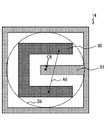
- FIG. 3 is a plan view showing a pixel electrode 50 and a control electrode 61 of the image pickup apparatus 101 according to the first embodiment.
- the line segment A1 and the circle B1 shown by the dotted lines are auxiliary lines for explanation.
- the control electrode 61 is a square and is arranged in the center of the unit pixel cell 14.
- the outer edge of the pixel electrode 50 is square and has a square opening.
- the control electrode 61 is arranged in the opening of the pixel electrode 50.
- the pixel electrode 50 completely surrounds the control electrode 61, but the pixel electrode 50 does not have to completely surround the control electrode 61.
- the pixel electrode 50 may have a C-shaped shape in which a part of the ring is missing, or may be divided into a plurality of parts.
- the control electrode 61 overlaps with the center point of the smallest circle completely including the pixel electrode 50 in a plan view.
- circle B1 represents the smallest circle that completely includes the pixel electrode 50.
- the point C1 indicates the center point of the circle B1.
- the center point C1 of the circle B1 overlaps with the control electrode 61.
- Such a condition means that the control electrode 61 is located near the center of the unit pixel cell 14 in a plan view.
- the vicinity of the central portion of the unit pixel cell 14 is a region focused by the microlens 55, and more signal charges are generated than the peripheral portion in the unit pixel cell 14.
- the sensitivity can be changed in a wide range depending on the voltage applied to the control electrode 61. Further, the higher the maximum sensitivity of the unit pixel cell 14, the wider the range in which the sensitivity can be changed by the voltage applied to the control electrode 61. In order to increase the maximum sensitivity of the unit pixel cell 14, it is desirable to increase the area of the pixel electrode 50 and bring it closer to the control electrode 61.
- the shortest distance between the center point C1 and the pixel electrode 50 may be, for example, half or less of the radius of the circle B1. As a result, a larger effect can be obtained.
- control electrode 61 may overlap with the point where the thickness of the microlens 55 becomes maximum in a plan view.
- the point C1 is also an example of the point where the thickness of the microlens 55 is maximized.
- the sensitivity can be changed in a wide range depending on the voltage applied to the control electrode 61 by arranging the point C1 at which the thickness of the microlens 55 is maximized so as to overlap the control electrode 61. ..
- the present embodiment there is a line segment connecting two points on the pixel electrode 50 and overlapping with the control electrode 61 in a plan view.
- the line segment A1 in FIG. 3 is an example of the above-mentioned line segment. As will be described in detail in the modification described later, the same effect can be obtained by arranging the line segments so as to exist.
- the holes generated in the photoelectric conversion layer 51 are pixelated by setting the potentials of the pixel electrode 50 and the control electrode 61 lower than those of the counter electrode 52. It can be collected on the electrode 50.
- a voltage of about 10 V is applied to the counter electrode 52. Further, the potential of the pixel electrode 50 is reset by turning the reset transistor 12 ON and then OFF. By resetting, the potential of the charge storage node 24 including the pixel electrode 50 is set to a reset voltage, for example, 0V as an initial value. Further, from the voltage application circuit 60, for example, a first sensitivity adjustment voltage lower than the reset voltage is applied to the control electrode 61. Here, as the first sensitivity adjustment voltage, a voltage of ⁇ 2V is applied to the control electrode 61.
- the potentials of the pixel electrode 50 and the control electrode 61 are set lower than those of the counter electrode 52. Therefore, the holes generated by the photoelectric conversion in the photoelectric conversion layer 51 move to the control electrode 61 and the pixel electrode 50.
- the voltage of the control electrode 61 is lower than the reset voltage of the pixel electrode 50. That is, the potential difference between the control electrode 61 and the counter electrode 52 is larger than the potential difference between the pixel electrode 50 and the counter electrode 52. Therefore, the generated holes are more likely to move to the control electrode 61 than to the pixel electrode 50. As a result, the holes generated in the region 51B (see FIG.
- the region 51B is a region of the photoelectric conversion layer 51 in which the signal charge (here, a hole) generated by the photoelectric conversion is mainly collected by the pixel electrode 50, and the region 51A is the region of the photoelectric conversion layer 51. Of these, this is a region in which the signal charge (here, holes) generated by photoelectric conversion mainly moves to the control electrode 61.
- FIG. 4B is a plan view of the region 51A as viewed from the pixel electrode 50 and the control electrode 61 side.
- the region 51A has a first area slightly larger than the control electrode 61 in a plane parallel to the photoelectric conversion layer 51.
- the shape and area of the region 51A when viewed from the direction perpendicular to the photoelectric conversion layer 51 do not necessarily match the shape and area of the control electrode 61.
- the shape and / or area of the region 51A may change depending on the voltage applied to the pixel electrode 50, the control electrode 61, and the counter electrode 52.
- the shape and area of the region 51B when viewed from the direction perpendicular to the photoelectric conversion layer 51 do not necessarily match the shape and area of the pixel electrode 50.
- 4A and 4B show the region 51A schematically, and there is no clear boundary between the region 51A and the region 51B.
- the signal charge is accumulated for each frame, and the accumulated charge and the potential of the pixel electrode 50 are reset. Thereby, the light incident on the photoelectric conversion layer 51 can be detected in the region 51B having the second area.
- 4C and 4D show an example in which the voltage application circuit 60 applies a second sensitivity adjustment voltage higher than the first sensitivity adjustment voltage to the control electrode 61.
- the second sensitivity adjustment voltage is 5V.
- the holes generated by the photoelectric conversion in the photoelectric conversion layer 51 move to the control electrode 61 and the pixel electrode 50 in the same manner as when the first sensitivity adjustment voltage is applied.
- the second sensitivity adjustment voltage here 5V
- the reset voltage here 0V
- a second sensitivity adjustment voltage higher than the first sensitivity adjustment voltage in the example described with reference to FIGS. 4A and 4B is applied to the control electrode 61. Therefore, the amount of holes flowing into the control electrode 61 is smaller than that when the first sensitivity adjusting voltage is applied to the control electrode 61. That is, the generated holes are more likely to move to the pixel electrode 50. As a result, as schematically shown in FIG. 4C, the region 51D in which the holes that can move to the pixel electrode 50 are distributed is compared with the region 51B when the first sensitivity adjustment voltage is applied to the control electrode 61. Will grow.
- the region 51C in which the holes that can move to the control electrode 61 are distributed is smaller than the region 51A (see FIG. 4A) when the first sensitivity adjustment voltage is applied to the control electrode 61.
- FIG. 4D is a plan view of the region 51C as viewed from the pixel electrode 50 and the control electrode 61 side.
- the region 51C has, for example, a third area smaller than the first area in a plane parallel to the photoelectric conversion layer 51.
- the region 51D has a fourth area that is larger than the second area when viewed from a direction perpendicular to the photoelectric conversion layer 51, for example.
- a signal charge is accumulated for each frame in a state where the second sensitivity adjustment voltage is applied to the control electrode 61, and the accumulated charge and the potential of the pixel electrode 50 are reset. Thereby, the light incident on the photoelectric conversion layer 51 can be detected in the region 51D having the fourth area.
- the region 51B in which the signal charge is captured by the pixel electrode 50 is relatively small
- the region 51B is relatively small
- the region 51D in which the signal charge is captured by the pixel electrode 50 is relatively large. That is, when the first sensitivity adjustment voltage is applied to the control electrode 61, the sensitivity of the image pickup apparatus 101 is relatively low, and when the second sensitivity adjustment voltage is applied, the sensitivity is relatively high. In this way, the sensitivity of the image pickup apparatus 101 can be changed by changing the sensitivity adjustment voltage Vc applied to the control electrode 61.
- the unit pixel cell 14 When the unit pixel cell 14 has a microlens, the light is focused on the central portion of the unit pixel cell 14 by the microlens. Therefore, a larger amount of signal charge is generated in the central portion of the unit pixel cell 14 than in the peripheral portion.
- the control electrode 61 by arranging the control electrode 61 in the central portion of the unit pixel cell 14, the destination of the signal charge generated in the central portion can be efficiently controlled by the voltage of the control electrode 61. This makes it possible to change the sensitivity in a wider range.
- the first sensitivity adjustment voltage and the second sensitivity adjustment voltage are examples, and the sensitivity adjustment voltage Vc is not limited to the above voltage value.
- the sensitivity is controlled by the control electrode 61, which is a third electrode, while maintaining a high electric field between the two terminals of the charge storage node 24 or the pixel electrode 50 and the counter electrode 52. Therefore, a region where the photocurrent between the two terminals is saturated can be used. By using the region where the photocurrent is saturated, even if the potential of the pixel electrode 50 changes due to the accumulation of signal charges, the influence on the photocurrent can be reduced. Thereby, according to the present embodiment, the sensitivity can be kept substantially constant with respect to the sensitivity adjustment voltage Vc.
- Vc the control electrode 61
- FIG. 5 is a diagram showing an example of the circuit configuration of the unit pixel cell 14 of the image pickup apparatus 101 according to the present embodiment.
- the photoelectric conversion unit 10 is schematically shown, but in FIG. 5, the photoelectric conversion unit 10 is illustrated by an equivalent circuit element.
- the unit pixel cell 14 includes an amplification transistor 11, a reset transistor 12, an address transistor 13, a laminated film capacity 10C, and a photoelectric conversion unit 10.
- the power supply voltage VDD supplied to the amplification transistor 11 are also added.
- the amplification transistor 11, the reset transistor 12, and the address transistor 13 constitute the charge detection circuit 25 as described above.
- One of the two electrodes constituting the laminated film capacity 10C corresponds to the control electrode 61, and the sensitivity adjustment voltage Vc is applied.
- the other electrode corresponds to the portion of the counter electrode 52 facing the control electrode 61. That is, the laminated film capacity 10C is a capacitor corresponding to a portion of the photoelectric conversion layer 51 sandwiched between the control electrode 61 and the counter electrode 52.
- the photoelectric conversion unit 10 is equivalent to a photodiode as a photoelectric conversion element.
- the cathode of the photodiode corresponds to the counter electrode 52.
- the anode corresponds to the pixel electrode 50.
- the charge storage node 24 is illustrated as a capacitor in FIG.
- the control electrode 61 to which the sensitivity adjustment voltage Vc is applied has a small parasitic capacitance with respect to the pixel electrode 50, the potential fluctuation of the pixel electrode 50 due to the change of the sensitivity adjustment voltage Vc becomes small.
- the control electrode 61 has a laminated film capacity of 10C corresponding to the facing electrode 52 facing the photoelectric conversion layer 51 as a dielectric.
- the counter electrode 52 is connected to the voltage application circuit 60, even if the potential of the counter electrode 52 changes due to the fluctuation of the sensitivity adjustment voltage Vc, the potential is immediately returned to a predetermined voltage. With such a configuration, even if the sensitivity adjustment voltage Vc is changed, the potentials of the two terminals of the counter electrode 52 and the pixel electrode 50 hardly change.
- FIG. 6 is a diagram showing an example of the relationship between the potential difference between the electrodes of the image pickup apparatus 101 according to the first embodiment and the photocurrent.
- the horizontal axis in the figure shows the potential of the counter electrode 52 with respect to the pixel electrode 50, that is, the potential difference between the pixel electrode 50 and the counter electrode 52.
- the vertical axis shows the magnitude of the photocurrent due to the electric charge generated by the incident light of a constant amount of light. That is, the characteristic of FIG. 6 shows the photocurrent-voltage characteristic between the two terminals in the absence of the control electrode 61, and shows the magnitude of the photocurrent when the voltage VITO is changed under a constant amount of light.
- the characteristics in the figure are roughly classified into a region Z, a linear region, and a saturated region according to the magnitude of the voltage VITO.
- the region Z is a region where the voltage VITO is in the vicinity of 0 V, and almost no photocurrent flows.
- the photocurrent increases substantially linearly with increasing voltage VITO.
- the saturated region the photocurrent does not change much even if the voltage VITO increases.
- the region where photocurrent is generated is divided into a linear region and a saturated region.
- the potential of the pixel electrode 50 changes due to the accumulation of signal charges, and the potential difference between the pixel electrode 50 and the counter electrode 52 changes.
- the photocurrent also changes with the potential change of the pixel electrode 50. That is, since the sensitivity fluctuates according to the amount of accumulated signal charge, the linearity of the signal output value is broken.
- the photoelectric conversion element when the photoelectric conversion element operates in the saturated region, the photocurrent does not change much even if the potential of the pixel electrode 50 changes. Therefore, the sensitivity is kept constant regardless of the accumulated amount of signal charge. Therefore, the signal output becomes linear with respect to the amount of incident light and the accumulation time.
- the potential of the pixel electrode 50 can rise up to approximately the same value as the potential of the counter electrode 52, but the potential of the pixel electrode 50 in which the signal can be detected is also limited by the voltage supplied to the amplification transistor 11. For example, by setting the potential of the counter electrode 52 to a sufficiently high value, it is possible to operate the photoelectric conversion element in the saturation region in the potential range of the pixel electrode 50 where the signal can be detected.
- the method of changing the sensitivity by the sensitivity adjustment voltage Vc of the control electrode 61 is suitable in that the linearity can be ensured in the saturated region rather than the linear region.
- FIG. 7 is a diagram showing an example of the relationship between the voltage applied to the control electrode 61 and the photocurrent in the image pickup apparatus 101 according to the first embodiment.
- the horizontal axis represents the sensitivity adjustment voltage Vc applied to the control electrode 61.
- the vertical axis shows the magnitude of the photocurrent corresponding to the electric charge generated by the incident light of a constant amount of light.
- FIG. 7 shows a case where the voltage VITO shown in FIG. 6 is within the range of the saturation region. That is, the photoelectric conversion characteristic of FIG. 7 indicates the magnitude of the photocurrent when the sensitivity adjustment voltage Vc is changed under a constant amount of light when the voltage VITO is within the saturation region of FIG.
- the sensitivity adjustment voltage Vc When the sensitivity adjustment voltage Vc is high, the holes generated in the photoelectric conversion layer 51 easily flow to the pixel electrode 50 side, so that the photocurrent increases and the sensitivity increases. When the sensitivity adjustment voltage Vc becomes sufficiently high, almost all the holes generated in the photoelectric conversion layer 51 flow to the pixel electrode 50, so that the sensitivity change is slowed down. On the contrary, when the sensitivity adjustment voltage Vc is low, the holes generated in the photoelectric conversion layer 51 easily flow to the control electrode 61, so that the photocurrent to the pixel electrode 50 decreases and the sensitivity becomes low.
- the signal charge is a hole, but the signal charge may be an electron.
- the signal charge is an electron
- a voltage higher than that of the counter electrode 52 is applied to the pixel electrode 50 and the control electrode 61.
- the electrons generated by the photoelectric conversion move to the pixel electrode 50 and the control electrode 61.
- the signal charge is an electron
- the smaller the sensitivity adjustment voltage Vc applied to the control electrode the easier it is for electrons to flow to the pixel electrode, and the higher the sensitivity of the image pickup device.
- the sensitivity adjustment voltage Vc applied to the control electrode is relatively high, electrons are likely to flow through the control electrode, and the sensitivity of the image pickup apparatus is low.
- the sensitivity of the image pickup apparatus 101 is changed by adjusting the sensitivity adjustment voltage Vc.
- the sensitivity of the image pickup apparatus is relatively low when the potential difference between the counter electrode 52 and the control electrode 61 is larger than the potential difference between the counter electrode 52 and the pixel electrode 50. Become.
- the potential difference between the counter electrode 52 and the control electrode 61 is smaller than the potential difference between the counter electrode 52 and the pixel electrode 50, the sensitivity of the image pickup apparatus becomes relatively high. This relationship holds even when the signal charge is an electron.
- the sensitivity adjustment voltage Vc applied to the control electrode 61 is between a value higher than the reset voltage of the pixel electrode 50 and a value equal to or lower than the reset voltage. It is changing with. However, even if the sensitivity adjustment voltage Vc applied to the control electrode 61 is changed in a range higher or lower than the reset voltage of the pixel electrode 50, the sensitivity of the image pickup apparatus 101 can be changed. For example, when the signal charge is a hole and the sensitivity adjustment voltage Vc is changed in a range lower than the reset voltage of the pixel electrode 50, the potential difference between the pixel electrode 50 and the control electrode 61 is relatively large. The larger the value, the lower the sensitivity of the image pickup device.
- FIG. 8 is a diagram showing a first modification example of the shapes of the control electrode 61 and the pixel electrode 50 of the image pickup apparatus 101 according to the first embodiment.
- the line segment A2 and the circle B2 shown by the dotted lines are auxiliary lines for explanation.
- This modification is different from the arrangement example shown in FIG. 3 in that a shield electrode 62 surrounding the pixel electrode 50 is added. A constant voltage is applied to the shield electrode 62. As a result, the shield electrode 62 prevents the signal charge from moving between the adjacent unit pixel cells 14 and prevents color mixing.
- the shield electrode 62 may be continuously formed over a plurality of unit pixel cells 14.
- the shield electrode 62 may be provided independently for each row, or may be provided independently for each pixel.
- the shield electrode 62 may be electrically connected to the control electrode 61. This makes it possible to reduce the number of independent power sources.
- FIG. 9 is a diagram showing a second modification example of the shapes of the control electrode 61 and the pixel electrode 50 of the image pickup apparatus 101 according to the first embodiment.
- the line segment A3 shown by the dotted line is an auxiliary line for explanation.
- the pixel electrode 50 has an H shape and is arranged in the center of the unit pixel cell 14.
- the control electrode 61 is arranged so as to surround the pixel electrode 50, and has a convex portion protruding toward the pixel electrode 50.
- the convex portion of the control electrode 61 extends toward the concave portion of the pixel electrode 50 so as to face the pixel electrode 50 on both sides thereof.
- the convex portion of the control electrode 61 is arranged so as to be inserted into the concave portion of the pixel electrode 50.
- the line segment A3 in FIG. 9 is an example of the above-mentioned line segment.
- the length of the side where the pixel electrode 50 and the control electrode 61 face each other becomes longer in a plan view. Therefore, the change range of the amount of the signal charge moving to the pixel electrode 50 can be widened by the sensitivity control voltage Vc applied to the control electrode 61. Further, according to this modification, the convex portion of the control electrode 61 is arranged near the center of the unit pixel cell 14. Therefore, the same effect as that described with reference to FIG. 3 can be obtained. Therefore, according to this modification, the sensitivity can be changed in a wider range.
- FIG. 10 is a diagram showing a third modification example of the shapes of the control electrode 61 and the pixel electrode 50 of the image pickup apparatus 101 according to the first embodiment.
- the line segment A4 shown by the dotted line is an auxiliary line for explanation.
- the pixel electrode 50 has a cross shape and is arranged in the center of the unit pixel cell 14.
- the control electrode 61 is arranged so as to surround the pixel electrode 50, and has a convex portion protruding toward the pixel electrode 50.
- the convex portion of the control electrode 61 extends toward the concave portion of the pixel electrode 50 so as to face the pixel electrode 50 on both sides thereof.
- the convex portion of the control electrode 61 is arranged so as to be inserted into the concave portion of the pixel electrode 50.
- the line segment A4 in FIG. 10 is an example of the above-mentioned line segment.
- the length of the side where the pixel electrode 50 and the control electrode 61 face each other becomes longer in a plan view. Therefore, the change range of the amount of the signal charge moving to the pixel electrode 50 can be widened by the sensitivity control voltage Vc applied to the control electrode 61. Further, according to this modification, the convex portion of the control electrode 61 is arranged near the center of the unit pixel cell 14. Therefore, the same effect as that described with reference to FIG. 3 can be obtained. Therefore, according to this modification, the sensitivity can be changed in a wider range.
- FIG. 11 is a diagram showing a fourth modification example of the shapes of the control electrode 61 and the pixel electrode 50 of the image pickup apparatus 101 according to the first embodiment.
- the line segment A5 and the circle B5 shown by the dotted lines are auxiliary lines for explanation.
- the pixel electrode 50 has a C shape.
- the control electrode 61 is arranged so as to surround the pixel electrode 50, and has a convex portion protruding toward the pixel electrode 50.
- the convex portion of the control electrode 61 extends toward the concave portion of the pixel electrode 50 so as to face the pixel electrode 50 on both sides thereof. That is, the convex portion of the control electrode 61 is arranged so as to be inserted into the concave portion of the pixel electrode 50.
- FIG. 11 there is a line segment connecting two points on the pixel electrode 50 and overlapping with the control electrode 61 in a plan view.
- the line segment A5 in FIG. 11 is an example of the above-mentioned line segment.
- the control electrode 61 overlaps with the center point of the smallest circle completely including the pixel electrode 50.
- circle B5 represents the smallest circle that completely includes the pixel electrode 50.
- C5 indicates the center point of the circle B5. As shown in FIG. 11, the center point C5 of the circle B5 overlaps with the control electrode 61.
- the length of the side where the pixel electrode 50 and the control electrode 61 face each other becomes longer in a plan view. Therefore, the change range of the amount of the signal charge moving to the pixel electrode 50 can be widened by the sensitivity control voltage Vc applied to the control electrode 61. Further, according to this modification, the convex portion of the control electrode 61 is arranged near the center of the unit pixel cell 14. Therefore, the same effect as that described with reference to FIG. 3 can be obtained. Therefore, according to this modification, the sensitivity can be changed in a wider range.
- FIG. 12 is a diagram showing a fifth modification example of the shapes of the control electrode 61 and the pixel electrode 50 of the image pickup apparatus 101 according to the first embodiment.
- the line segment A6 and the circle B6 shown by the dotted lines are auxiliary lines for explanation.
- the unit pixel cell 14 in the image pickup apparatus 101 includes two pixel electrodes 50, each of which is rectangular.
- the control electrode 61 is arranged so as to surround each of the two pixel electrodes 50, and has a portion extending between the two pixel electrodes 50.
- the line segment A6 in FIG. 12 is an example of the above-mentioned line segment.
- the control electrode 61 overlaps with the center point of the smallest circle completely including the pixel electrode 50.
- circle B6 represents the smallest circle that completely includes the pixel electrode 50.
- C6 indicates the center point of the circle B6. As shown in FIG. 12, the center point C6 of the circle B6 overlaps with the control electrode 61.
- the length of the side where the pixel electrode 50 and the control electrode 61 face each other becomes longer in a plan view. Therefore, the change range of the amount of the signal charge moving to the pixel electrode 50 can be widened by the sensitivity control voltage Vc applied to the control electrode 61. Further, according to this modification, a part of the control electrode 61 is arranged near the center of the unit pixel cell 14. Therefore, the same effect as that described with reference to FIG. 3 can be obtained. Therefore, according to this modification, the sensitivity can be changed in a wider range.
- FIG. 13 is a timing chart showing an example of the operation of the image pickup apparatus 101 according to the first embodiment.
- the figure shows an example of the timing of application and exposure of the sensitivity adjustment voltage Vc when the sensitivity adjustment voltage Vc is changed in the image pickup apparatus 101.
- RST1, RST2, RST3, RST4, ..., RSTn are applied to the gate electrodes of the reset transistor 12 constituting the first, second, third, fourth, ..., Nth rows, respectively. It shows the timing of the gate voltage (also called the reset gate voltage).
- the image pickup apparatus 101 performs exposure and signal reading line by line, for example. Therefore, by applying the reset gate voltage, the charge storage node 24 in the unit pixel cell 14 in each row is sequentially reset during the period of one frame. In each row of the pixel array, the period from the application of the reset gate voltage to the application of the next reset gate voltage corresponds to the exposure time.
- the sensitivity adjustment voltage Vc applied to the control electrode 61 is changed at the start timing of the second frame.
- the sensitivity adjustment voltage Vc applied to the control electrode 61 is controlled at the same timing as a whole, not for each row. While the sensitivity adjustment voltage Vc is controlled at the same timing in the entire pixel array, the timing of the exposure start of each row of pixels is deviated from row to row, as can be seen from FIG. Therefore, no matter when the sensitivity adjustment voltage Vc applied to the control electrode 61 is changed, the sensitivity adjustment voltage Vc changes during the exposure time.
- the sensitivity adjustment voltage Vc In the frame in which the sensitivity adjustment voltage Vc is changed (here, the second frame), the sensitivity is different for each row, and the sensitivity adjustment voltage Vc changes in the middle of the exposure period, so that it corresponds to the sensitivity adjustment voltage Vc to be applied. It is not possible to detect incident light with the correct sensitivity. Therefore, the image data captured in the second frame in which the sensitivity adjustment voltage Vc is changed is discarded. In the next third frame, since the changed sensitivity adjustment voltage Vc is applied to any row from the start of exposure, it is possible to detect the incident light with the correct sensitivity in all the rows.
- the sensitivity of the image pickup apparatus can be changed in frame units by changing the value of the sensitivity adjustment voltage Vc supplied from the voltage application circuit. Therefore, it is possible to realize an image pickup device capable of taking a picture with high image quality even in various environments where the brightness changes greatly.
- control electrodes 61 of each unit pixel cell 14 are connected to each other, the wiring for driving the control electrodes can be reduced.
- the sensitivity adjustment voltage Vc applied to the control electrode 61 is changed in units of 2 frames.
- the switching of the sensitivity adjustment voltage Vc is not limited to the unit of two frames. As described below, it is also possible to switch the sensitivity adjustment voltage Vc in units of one frame.
- FIG. 14 is a timing chart showing another example of the operation of the image pickup apparatus 101 according to the first embodiment.
- the figure shows another example of timing of application of sensitivity adjustment voltage Vc, exposure, and signal readout.
- the voltage application circuit 60 switches the sensitivity adjustment voltage Vc from V0 to Vs during one frame, and further switches the sensitivity adjustment voltage Vc to V0 again after a lapse of a certain period of time Te.
- the voltage V0 is a voltage sufficiently low enough to make the sensitivity of the image pickup apparatus 101 almost zero. That is, in a state where the voltage V0 is applied to the control electrode 61, most of the signal charges (here, holes) generated in the photoelectric conversion layer 51 are captured by the control electrode 61. In other words, when the voltage V0 is applied to the control electrode 61, the region where the signal charge is captured by the pixel electrode 50 (for example, the region 51B shown in FIGS. 4A and 4B) is sufficiently small. The signal charge captured by the pixel electrode 50 is very small. That is, by applying the voltage V0 to the control electrode 61, it is possible to realize a state as if the photosensitive area is shielded from light.
- the image pickup device 101 has the sensitivity required for photographing. be able to.
- the voltage Vs is applied to the control electrode 61 in a certain period within one frame, and the voltage V0 is applied in the other period. Therefore, the collection of the signal charge by the pixel electrode 50 is executed except for the period in which the sensitivity is almost 0 and the voltage V0 is applied to the control electrode 61. That is, the period Te in which the voltage Vs is applied to the control electrode 61 in one frame contributes to the accumulation of the signal charge as an effective exposure time.
- the effective exposure time can be adjusted by the period in which the voltage Vs is applied to the control electrode 61. As shown in FIG. 14, this effective exposure time may be common to all unit pixel cells 14. Therefore, it is possible to make the exposure periods of all the unit pixel cells included in the pixel array uniform. That is, by changing the sensitivity adjustment voltage Vc within one frame, it is possible to realize the same function as the so-called global shutter without separately providing a capacitive element or the like for accumulating signal charges in the pixel.
- the waveform of the sensitivity adjustment voltage Vc applied to the period Te is not limited to the rectangular pulse as shown by the solid line in FIG. 14, but may be a triangular wave as shown by the dotted line.
- FIG. 15 is a timing chart showing still another example of the operation of the image pickup apparatus 101 according to the first embodiment.
- the figure shows yet another example of the timing of application of the sensitivity adjustment voltage Vc, exposure, and signal readout.
- V0 of an appropriate magnitude
- the sensitivity of the image pickup apparatus 101 can be reduced to almost zero. That is, the sensitivity adjustment voltage Vc applied to the control electrode 61 can be used instead of the shutter.
- the accumulation of signal charges is performed during the period when the voltage Vs is applied to the control electrode 61. The period in which the voltage V0 is applied to the control electrode 61 does not effectively contribute to image acquisition.
- the voltage application circuit 60 periodically switches the sensitivity adjustment voltage Vc to V0 and Vs during one frame. Therefore, the effective exposure period and the non-exposure period are periodically repeated. For example, when shooting under a lighting fixture having periodic flicker, the influence of the periodic flicker of the lighting fixture can be canceled by periodically changing the voltage applied to the control electrode 61.
- FIG. 16 is a timing chart showing still another example of the operation of the image pickup apparatus according to the first embodiment.
- the figure shows yet another example of the timing of application of the sensitivity adjustment voltage Vc, exposure, and signal readout.
- the sensitivity adjustment voltage Vc applied to the control electrode 61 is controlled at different timings for each row.
- Vc1, Vc2, Vc3, Vc4, ..., Vcn indicate the timing of change in the sensitivity adjustment voltage Vc applied to the control electrode 61 of the unit pixel cell 14 in the first row to the nth row, respectively. ing.
- the sensitivity adjustment voltage Vc is changed according to the timing of switching the reset gate voltage from the high level to the low level.
- the sensitivity adjustment voltage Vc in each frame can be made constant in each row of the unit pixel cell 14. That is, the sensitivity can be changed on a frame-by-frame basis for each line.
- the image pickup apparatus of the present embodiment can adjust the sensitivity in frame units, it responds to the change in brightness at high speed and adjusts the sensitivity even in a shooting environment where the brightness changes rapidly. It is possible.
- the image pickup device according to the present disclosure is useful for image pickup devices such as digital cameras and image sensors.
- Photoelectric conversion unit 10C Laminated film capacity 11 Amplification transistor 12 Reset transistor 13 Address transistor 14 Unit pixel cell 15 Vertical scanning circuit 16 Photoelectric conversion unit control line 17 Vertical signal line 18 Load circuit 19 Column signal processing circuit 20 Horizontal signal readout circuit 21 Power supply Wiring 22 Inversion amplifier 23 Feedback line 24 Charge storage node 25 Charge detection circuit 26 Address signal line 27 Reset signal line 28 Sensitivity adjustment line 29 Horizontal common signal line 31 Semiconductor substrate 38A Gate insulation layer 38C Gate insulation layer 39A Gate electrode 39C Gate electrode 41C n-type impurity region 41D n-type impurity region 42 Element separation region 43A Interlayer insulation layer 43C Interlayer insulation layer 45A Contact plugs 46A, 46C, 49 Wiring 48A, 48B, 48C Plug 50 Pixel electrode 51 Transistor conversion layer 51A, 51B, 51C, 51D Region 52 Opposing electrode 53 Sealing film 54 Color filter 55 Microlens 60 Voltage application circuit 61 Control electrode 62 Shielding electrode 101 Image pickup device L1 Distance Vc Sensitivity adjustment voltage
Landscapes
- Engineering & Computer Science (AREA)
- Physics & Mathematics (AREA)
- Power Engineering (AREA)
- Electromagnetism (AREA)
- Condensed Matter Physics & Semiconductors (AREA)
- General Physics & Mathematics (AREA)
- Computer Hardware Design (AREA)
- Microelectronics & Electronic Packaging (AREA)
- Multimedia (AREA)
- Signal Processing (AREA)
- Solid State Image Pick-Up Elements (AREA)
- Transforming Light Signals Into Electric Signals (AREA)
Abstract
Description
特許文献1に記載の技術は、対向電極の電圧を変化させることにより、感度を変化させている。しかし、信号電荷の蓄積によって画素電極の電位が変化するため、対向電極の電圧に対して感度を一定に保てない。すなわち、対向電極の電位をある値に設定しても、信号電荷の蓄積によって感度が変化してしまう。
図1から図3を参照しながら、本実施形態に係る撮像装置を説明する。
図1は、第1の実施形態に係る撮像装置101の回路構成の一例を、模式的に示している。撮像装置101は、複数の単位画素セル14と、周辺回路とを備えている。
図2は、本実施形態に係る撮像装置101中の単位画素セル14の、デバイス構造の断面を模式的に示す断面図である。
次に図1、図2および図4Aから図4Dを参照しながら、撮像装置101の例示的な動作を説明する。以下に説明するように、信号電荷が正孔である場合には、対向電極52よりも画素電極50および制御電極61の電位を低く設定することにより、光電変換層51で発生した正孔を画素電極50に集めることができる。
図8から図12を用いて、制御電極61および画素電極50の形状および配置の変形例を説明する。
次に、図13から図16を参照しながら、撮像装置101の例示的な駆動方法を説明する。図13は、実施形態1に係る撮像装置101の動作の一例を示すタイミングチャートである。同図は、撮像装置101において感度調整電圧Vcを変化させる場合における、感度調整電圧Vcの印加および露光のタイミングの一例を示している。
10C 積層膜容量
11 増幅トランジスタ
12 リセットトランジスタ
13 アドレストランジスタ
14 単位画素セル
15 垂直走査回路
16 光電変換部制御線
17 垂直信号線
18 負荷回路
19 カラム信号処理回路
20 水平信号読出し回路
21 電源配線
22 反転増幅器
23 フィードバック線
24 電荷蓄積ノード
25 電荷検出回路
26 アドレス信号線
27 リセット信号線
28 感度調整線
29 水平共通信号線
31 半導体基板
38A ゲート絶縁層
38C ゲート絶縁層
39A ゲート電極
39C ゲート電極
41C n型不純物領域
41D n型不純物領域
42 素子分離領域
43A 層間絶縁層
43C 層間絶縁層
45A コンタクトプラグ
46A、46C、49 配線
48A、48B、48C プラグ
50 画素電極
51 光電変換層
51A、51B、51C、51D 領域
52 対向電極
53 封止膜
54 カラーフィルタ
55 マイクロレンズ
60 電圧印加回路
61 制御電極
62 シールド電極
101 撮像装置
L1 距離
Vc 感度調整電圧
Claims (12)
- 第1面と前記第1面に対向する第2面とを有し、信号電荷を生成する光電変換層と、
前記光電変換層の前記第1面上に位置する少なくとも1つの画素電極と、
前記光電変換層の前記第1面上に位置し、感度を制御するための制御電極と、
前記光電変換層の前記第2面上に位置し、前記少なくとも1つの画素電極および前記制御電極と対向する対向電極と、
前記少なくとも1つの画素電極に接続され、前記信号電荷を蓄積する電荷蓄積部と、
を備え、
前記少なくとも1つの画素電極上の2点を結ぶ線分であって、平面視において前記制御電極と重なる線分が存在する、
撮像装置。 - 平面視において、前記制御電極は、前記少なくとも1つの画素電極によって囲まれている、
請求項1に記載の撮像装置。 - 平面視において、前記制御電極は、前記少なくとも1つの画素電極を完全に含む最小の円の中心と重なる、
請求項1または2に記載の撮像装置。 - 前記第2面の上方に位置するマイクロレンズをさらに備える、
請求項1から3のいずれか1項に記載の撮像装置。 - 平面視において、前記制御電極は、前記マイクロレンズの厚みが最大となる点と重なる、
請求項4に記載の撮像装置。 - 前記光電変換層は、有機材料を含む、
請求項1から5のいずれか1項に記載の撮像装置。 - 前記第1面上に位置し、平面視において前記少なくとも1つの画素電極および前記制御電極を囲むシールド電極をさらに備える、
請求項1から6のいずれか1項に記載の撮像装置。 - 前記制御電極は、前記シールド電極と電気的に接続されている、
請求項7に記載の撮像装置。 - 電圧供給回路をさらに備え、
前記信号電荷は正孔であり、
前記電圧供給回路は、前記対向電極に第1電圧を供給し、前記制御電極に前記第1電圧以下の第2電圧を供給する、
請求項1から8のいずれか1項に記載の撮像装置。 - 前記電圧供給回路は、前記制御電極に、第1フレーム期間において前記第2電圧を供給し、前記第1フレーム期間と異なる第2フレーム期間において前記第2電圧より低い第3電圧を供給する、
請求項9に記載の撮像装置。 - 第1面と前記第1面に対向する第2面とを有し、信号電荷を生成する光電変換層と、
前記光電変換層の前記第1面上に位置する少なくとも1つの画素電極と、
前記光電変換層の前記第1面上に位置し、感度を制御するための制御電極と、
前記光電変換層の前記第2面上に位置し、前記少なくとも1つの画素電極および前記制御電極と対向する対向電極と、
前記少なくとも1つの画素電極に接続され、前記信号電荷を蓄積する電荷蓄積部と、
を備え、
平面視において、前記制御電極は、前記少なくとも1つの画素電極を完全に含む最小の円の中心と重なる、
撮像装置。 - 第1面と前記第1面に対向する第2面とを有し、信号電荷を生成する光電変換層と、
前記光電変換層の前記第1面上に位置する少なくとも1つの画素電極と、
前記光電変換層の前記第1面上に位置し、感度を制御するための制御電極と、
前記光電変換層の前記第2面上に位置し、前記少なくとも1つの画素電極および前記制御電極と対向する対向電極と、
前記光電変換層の前記第2面の上方に位置するマイクロレンズと、
前記少なくとも1つの画素電極に接続され、前記信号電荷を蓄積する電荷蓄積部と、
を備え、
平面視において、前記制御電極は、前記マイクロレンズの厚みが最大となる点と重なる、
撮像装置。
Priority Applications (3)
| Application Number | Priority Date | Filing Date | Title |
|---|---|---|---|
| CN202180079297.3A CN116491127A (zh) | 2020-12-15 | 2021-11-09 | 摄像装置 |
| JP2022569769A JPWO2022130835A1 (ja) | 2020-12-15 | 2021-11-09 | |
| US18/322,621 US20230299098A1 (en) | 2020-12-15 | 2023-05-24 | Imaging device |
Applications Claiming Priority (2)
| Application Number | Priority Date | Filing Date | Title |
|---|---|---|---|
| JP2020207889 | 2020-12-15 | ||
| JP2020-207889 | 2020-12-15 |
Related Child Applications (1)
| Application Number | Title | Priority Date | Filing Date |
|---|---|---|---|
| US18/322,621 Continuation US20230299098A1 (en) | 2020-12-15 | 2023-05-24 | Imaging device |
Publications (1)
| Publication Number | Publication Date |
|---|---|
| WO2022130835A1 true WO2022130835A1 (ja) | 2022-06-23 |
Family
ID=82057552
Family Applications (1)
| Application Number | Title | Priority Date | Filing Date |
|---|---|---|---|
| PCT/JP2021/041249 WO2022130835A1 (ja) | 2020-12-15 | 2021-11-09 | 撮像装置 |
Country Status (4)
| Country | Link |
|---|---|
| US (1) | US20230299098A1 (ja) |
| JP (1) | JPWO2022130835A1 (ja) |
| CN (1) | CN116491127A (ja) |
| WO (1) | WO2022130835A1 (ja) |
Citations (6)
| Publication number | Priority date | Publication date | Assignee | Title |
|---|---|---|---|---|
| JPH09331051A (ja) * | 1995-06-16 | 1997-12-22 | S I I R D Center:Kk | 光電変換半導体装置 |
| JP2008277797A (ja) * | 2007-03-30 | 2008-11-13 | Panasonic Electric Works Co Ltd | 撮像素子 |
| JP2016086407A (ja) * | 2014-10-23 | 2016-05-19 | パナソニックIpマネジメント株式会社 | 撮像装置および画像取得装置 |
| JP2018085402A (ja) * | 2016-11-22 | 2018-05-31 | ソニー株式会社 | 撮像素子、積層型撮像素子及び固体撮像装置 |
| WO2019044103A1 (ja) * | 2017-08-31 | 2019-03-07 | ソニーセミコンダクタソリューションズ株式会社 | 撮像素子、積層型撮像素子及び固体撮像装置 |
| WO2020022100A1 (ja) * | 2018-07-27 | 2020-01-30 | ソニーセミコンダクタソリューションズ株式会社 | 撮像素子、電子機器 |
-
2021
- 2021-11-09 JP JP2022569769A patent/JPWO2022130835A1/ja active Pending
- 2021-11-09 CN CN202180079297.3A patent/CN116491127A/zh active Pending
- 2021-11-09 WO PCT/JP2021/041249 patent/WO2022130835A1/ja active Application Filing
-
2023
- 2023-05-24 US US18/322,621 patent/US20230299098A1/en active Pending
Patent Citations (6)
| Publication number | Priority date | Publication date | Assignee | Title |
|---|---|---|---|---|
| JPH09331051A (ja) * | 1995-06-16 | 1997-12-22 | S I I R D Center:Kk | 光電変換半導体装置 |
| JP2008277797A (ja) * | 2007-03-30 | 2008-11-13 | Panasonic Electric Works Co Ltd | 撮像素子 |
| JP2016086407A (ja) * | 2014-10-23 | 2016-05-19 | パナソニックIpマネジメント株式会社 | 撮像装置および画像取得装置 |
| JP2018085402A (ja) * | 2016-11-22 | 2018-05-31 | ソニー株式会社 | 撮像素子、積層型撮像素子及び固体撮像装置 |
| WO2019044103A1 (ja) * | 2017-08-31 | 2019-03-07 | ソニーセミコンダクタソリューションズ株式会社 | 撮像素子、積層型撮像素子及び固体撮像装置 |
| WO2020022100A1 (ja) * | 2018-07-27 | 2020-01-30 | ソニーセミコンダクタソリューションズ株式会社 | 撮像素子、電子機器 |
Also Published As
| Publication number | Publication date |
|---|---|
| JPWO2022130835A1 (ja) | 2022-06-23 |
| US20230299098A1 (en) | 2023-09-21 |
| CN116491127A (zh) | 2023-07-25 |
Similar Documents
| Publication | Publication Date | Title |
|---|---|---|
| JP6872707B2 (ja) | 撮像装置および画像取得装置 | |
| US11532652B2 (en) | Imaging device and image acquisition device | |
| JP6982823B2 (ja) | 撮像装置およびその駆動方法 | |
| US9894297B2 (en) | Imaging device | |
| CN106954008B (zh) | 摄像装置及摄像模块 | |
| CN108878462B (zh) | 摄像装置及照相机系统 | |
| CN106254726B (zh) | 摄像装置及摄像模块 | |
| US10057518B2 (en) | Imaging device and image acquisition device | |
| JP6587123B2 (ja) | 撮像装置 | |
| US20230215882A1 (en) | Imaging device | |
| US10194104B2 (en) | Imaging device and imaging module | |
| WO2022130835A1 (ja) | 撮像装置 | |
| US20210258520A1 (en) | Imaging device | |
| JP2021057885A (ja) | 撮像装置およびその駆動方法 | |
| JP2016197644A (ja) | 撮像装置 | |
| JPWO2020054162A1 (ja) | 撮像装置および撮像方法 | |
| US20230292017A1 (en) | Imaging device | |
| WO2023079795A1 (ja) | 撮像装置 | |
| US20230262364A1 (en) | Imaging device | |
| WO2023199560A1 (ja) | 撮像装置およびカメラシステム | |
| CN116547815A (zh) | 显示装置及其制造方法 | |
| JP2009177009A (ja) | 撮像装置及び固体撮像素子の駆動方法 |
Legal Events
| Date | Code | Title | Description |
|---|---|---|---|
| 121 | Ep: the epo has been informed by wipo that ep was designated in this application |
Ref document number: 21906199 Country of ref document: EP Kind code of ref document: A1 |
|
| WWE | Wipo information: entry into national phase |
Ref document number: 202180079297.3 Country of ref document: CN |
|
| ENP | Entry into the national phase |
Ref document number: 2022569769 Country of ref document: JP Kind code of ref document: A |
|
| NENP | Non-entry into the national phase |
Ref country code: DE |
|
| 122 | Ep: pct application non-entry in european phase |
Ref document number: 21906199 Country of ref document: EP Kind code of ref document: A1 |