WO2022102282A1 - 発光装置、発光装置の駆動方法、及び、電子機器 - Google Patents
発光装置、発光装置の駆動方法、及び、電子機器 Download PDFInfo
- Publication number
- WO2022102282A1 WO2022102282A1 PCT/JP2021/036671 JP2021036671W WO2022102282A1 WO 2022102282 A1 WO2022102282 A1 WO 2022102282A1 JP 2021036671 W JP2021036671 W JP 2021036671W WO 2022102282 A1 WO2022102282 A1 WO 2022102282A1
- Authority
- WO
- WIPO (PCT)
- Prior art keywords
- light emitting
- unit
- control unit
- gradation
- light
- Prior art date
- Legal status (The legal status is an assumption and is not a legal conclusion. Google has not performed a legal analysis and makes no representation as to the accuracy of the status listed.)
- Ceased
Links
Images








Classifications
-
- G—PHYSICS
- G09—EDUCATION; CRYPTOGRAPHY; DISPLAY; ADVERTISING; SEALS
- G09G—ARRANGEMENTS OR CIRCUITS FOR CONTROL OF INDICATING DEVICES USING STATIC MEANS TO PRESENT VARIABLE INFORMATION
- G09G3/00—Control arrangements or circuits, of interest only in connection with visual indicators other than cathode-ray tubes
- G09G3/20—Control arrangements or circuits, of interest only in connection with visual indicators other than cathode-ray tubes for presentation of an assembly of a number of characters, e.g. a page, by composing the assembly by combination of individual elements arranged in a matrix no fixed position being assigned to or needed to be assigned to the individual characters or partial characters
- G09G3/22—Control arrangements or circuits, of interest only in connection with visual indicators other than cathode-ray tubes for presentation of an assembly of a number of characters, e.g. a page, by composing the assembly by combination of individual elements arranged in a matrix no fixed position being assigned to or needed to be assigned to the individual characters or partial characters using controlled light sources
- G09G3/30—Control arrangements or circuits, of interest only in connection with visual indicators other than cathode-ray tubes for presentation of an assembly of a number of characters, e.g. a page, by composing the assembly by combination of individual elements arranged in a matrix no fixed position being assigned to or needed to be assigned to the individual characters or partial characters using controlled light sources using electroluminescent panels
- G09G3/32—Control arrangements or circuits, of interest only in connection with visual indicators other than cathode-ray tubes for presentation of an assembly of a number of characters, e.g. a page, by composing the assembly by combination of individual elements arranged in a matrix no fixed position being assigned to or needed to be assigned to the individual characters or partial characters using controlled light sources using electroluminescent panels semiconductive, e.g. using light-emitting diodes [LED]
- G09G3/3208—Control arrangements or circuits, of interest only in connection with visual indicators other than cathode-ray tubes for presentation of an assembly of a number of characters, e.g. a page, by composing the assembly by combination of individual elements arranged in a matrix no fixed position being assigned to or needed to be assigned to the individual characters or partial characters using controlled light sources using electroluminescent panels semiconductive, e.g. using light-emitting diodes [LED] organic, e.g. using organic light-emitting diodes [OLED]
- G09G3/3225—Control arrangements or circuits, of interest only in connection with visual indicators other than cathode-ray tubes for presentation of an assembly of a number of characters, e.g. a page, by composing the assembly by combination of individual elements arranged in a matrix no fixed position being assigned to or needed to be assigned to the individual characters or partial characters using controlled light sources using electroluminescent panels semiconductive, e.g. using light-emitting diodes [LED] organic, e.g. using organic light-emitting diodes [OLED] using an active matrix
- G09G3/3233—Control arrangements or circuits, of interest only in connection with visual indicators other than cathode-ray tubes for presentation of an assembly of a number of characters, e.g. a page, by composing the assembly by combination of individual elements arranged in a matrix no fixed position being assigned to or needed to be assigned to the individual characters or partial characters using controlled light sources using electroluminescent panels semiconductive, e.g. using light-emitting diodes [LED] organic, e.g. using organic light-emitting diodes [OLED] using an active matrix with pixel circuitry controlling the current through the light-emitting element
-
- G—PHYSICS
- G09—EDUCATION; CRYPTOGRAPHY; DISPLAY; ADVERTISING; SEALS
- G09G—ARRANGEMENTS OR CIRCUITS FOR CONTROL OF INDICATING DEVICES USING STATIC MEANS TO PRESENT VARIABLE INFORMATION
- G09G3/00—Control arrangements or circuits, of interest only in connection with visual indicators other than cathode-ray tubes
- G09G3/20—Control arrangements or circuits, of interest only in connection with visual indicators other than cathode-ray tubes for presentation of an assembly of a number of characters, e.g. a page, by composing the assembly by combination of individual elements arranged in a matrix no fixed position being assigned to or needed to be assigned to the individual characters or partial characters
- G09G3/2007—Display of intermediate tones
- G09G3/2018—Display of intermediate tones by time modulation using two or more time intervals
- G09G3/2022—Display of intermediate tones by time modulation using two or more time intervals using sub-frames
- G09G3/2025—Display of intermediate tones by time modulation using two or more time intervals using sub-frames the sub-frames having all the same time duration
-
- G—PHYSICS
- G09—EDUCATION; CRYPTOGRAPHY; DISPLAY; ADVERTISING; SEALS
- G09G—ARRANGEMENTS OR CIRCUITS FOR CONTROL OF INDICATING DEVICES USING STATIC MEANS TO PRESENT VARIABLE INFORMATION
- G09G3/00—Control arrangements or circuits, of interest only in connection with visual indicators other than cathode-ray tubes
- G09G3/20—Control arrangements or circuits, of interest only in connection with visual indicators other than cathode-ray tubes for presentation of an assembly of a number of characters, e.g. a page, by composing the assembly by combination of individual elements arranged in a matrix no fixed position being assigned to or needed to be assigned to the individual characters or partial characters
- G09G3/2092—Details of a display terminals using a flat panel, the details relating to the control arrangement of the display terminal and to the interfaces thereto
- G09G3/2096—Details of the interface to the display terminal specific for a flat panel
-
- H—ELECTRICITY
- H10—SEMICONDUCTOR DEVICES; ELECTRIC SOLID-STATE DEVICES NOT OTHERWISE PROVIDED FOR
- H10H—INORGANIC LIGHT-EMITTING SEMICONDUCTOR DEVICES HAVING POTENTIAL BARRIERS
- H10H20/00—Individual inorganic light-emitting semiconductor devices having potential barriers, e.g. light-emitting diodes [LED]
- H10H20/80—Constructional details
-
- G—PHYSICS
- G09—EDUCATION; CRYPTOGRAPHY; DISPLAY; ADVERTISING; SEALS
- G09G—ARRANGEMENTS OR CIRCUITS FOR CONTROL OF INDICATING DEVICES USING STATIC MEANS TO PRESENT VARIABLE INFORMATION
- G09G2310/00—Command of the display device
- G09G2310/02—Addressing, scanning or driving the display screen or processing steps related thereto
- G09G2310/0243—Details of the generation of driving signals
- G09G2310/0259—Details of the generation of driving signals with use of an analog or digital ramp generator in the column driver or in the pixel circuit
-
- G—PHYSICS
- G09—EDUCATION; CRYPTOGRAPHY; DISPLAY; ADVERTISING; SEALS
- G09G—ARRANGEMENTS OR CIRCUITS FOR CONTROL OF INDICATING DEVICES USING STATIC MEANS TO PRESENT VARIABLE INFORMATION
- G09G2310/00—Command of the display device
- G09G2310/08—Details of timing specific for flat panels, other than clock recovery
-
- G—PHYSICS
- G09—EDUCATION; CRYPTOGRAPHY; DISPLAY; ADVERTISING; SEALS
- G09G—ARRANGEMENTS OR CIRCUITS FOR CONTROL OF INDICATING DEVICES USING STATIC MEANS TO PRESENT VARIABLE INFORMATION
- G09G2320/00—Control of display operating conditions
- G09G2320/02—Improving the quality of display appearance
- G09G2320/0233—Improving the luminance or brightness uniformity across the screen
-
- G—PHYSICS
- G09—EDUCATION; CRYPTOGRAPHY; DISPLAY; ADVERTISING; SEALS
- G09G—ARRANGEMENTS OR CIRCUITS FOR CONTROL OF INDICATING DEVICES USING STATIC MEANS TO PRESENT VARIABLE INFORMATION
- G09G2320/00—Control of display operating conditions
- G09G2320/02—Improving the quality of display appearance
- G09G2320/0242—Compensation of deficiencies in the appearance of colours
-
- G—PHYSICS
- G09—EDUCATION; CRYPTOGRAPHY; DISPLAY; ADVERTISING; SEALS
- G09G—ARRANGEMENTS OR CIRCUITS FOR CONTROL OF INDICATING DEVICES USING STATIC MEANS TO PRESENT VARIABLE INFORMATION
- G09G2320/00—Control of display operating conditions
- G09G2320/02—Improving the quality of display appearance
- G09G2320/0271—Adjustment of the gradation levels within the range of the gradation scale, e.g. by redistribution or clipping
- G09G2320/0276—Adjustment of the gradation levels within the range of the gradation scale, e.g. by redistribution or clipping for the purpose of adaptation to the characteristics of a display device, i.e. gamma correction
Definitions
- the present disclosure relates to a light emitting device, a driving method of the light emitting device, and an electronic device.
- a light emitting device in which light emitting units are arranged in a matrix (two-dimensional matrix shape) in the row direction and the column direction is a self-luminous display device or a backlight device of a liquid crystal display device. And so on.
- a self-luminous element such as a light emitting diode (LED) or an organic EL (electroluminescence) element can be exemplified.
- LED light emitting diode
- organic EL electroluminescence
- the light emitting diode has a characteristic that the spectrum shifts to the blue side by the current (light emitting current) flowing through the element, and accordingly, the chromaticity fluctuates depending on the value of the light emitting current, or in a low current region. It is known that there is a large variation in brightness. Therefore, when a light emitting device is configured using a light emitting diode, if the light emitting current is changed by current modulation or voltage modulation to control the luminance, the color cannot be accurately expressed by the luminance and uneven luminance occurs at low luminance. There is a problem such as
- a PWM (Pulse Width Modulation) drive that changes the duty ratio of a light emitting section to perform modulation, or a plurality of fields are used.
- Subfield driving is known in which driving is performed by dividing into subfields.
- Patent Document 1 Japanese Unexamined Patent Publication No. 2007-3337678 discloses a technique of using PWM drive for driving a light emitting unit and a technique of using subfield drive.
- PWM drive with high resolution is vulnerable to noise and various fluctuations, and its implementation requires a circuit configuration with a large circuit scale.
- display devices that use the PWM drive of the passive matrix, but there are problems such as low brightness due to the inability to obtain a large emission duty, and the increase in the number of drivers and high cost when the definition is increased. be.
- the subfield drive does not require a larger circuit scale than the PWM drive.
- the gamma characteristic becomes linear, and there is a problem that the resolution of low gradation is particularly insufficient.
- the problem has been described by taking an LED display device that uses a light emitting diode as a light emitting unit as an example.
- the above-mentioned points are not limited to the LED display device that uses a light emitting diode as a light emitting unit, and the self-luminous element can be used. This is a problem that can be said for all light emitting devices arranged in a two-dimensional matrix.
- the light emitting device is Pixel circuit including light emitting part and Gradation control unit that controls gradation, Equipped with The pixel circuit is A light emitting time control unit that controls the light emitting time of the light emitting unit, and a light emitting unit.
- Amplitude modulator including an output transistor connected in series with the light emitting unit, Have,
- the gradation control unit performs gradation control by performing on / off control of the output transistor of the amplitude modulation unit and modulation control of the amplitude modulation unit via the light emission time control unit.
- Pixel circuit including light emitting part and Gradation control unit that controls gradation
- the pixel circuit is A light emitting time control unit that controls the light emitting time of the light emitting unit, and a light emitting unit.
- Amplitude modulator including an output transistor connected in series with the light emitting unit, In a light emitting device having Under the control of the gradation control unit, the output transistor of the amplitude modulation unit is turned on / off, and the modulation control of the amplitude modulation unit is performed to control the gradation.
- the electronic device is Gradation control unit that controls gradation, Equipped with The pixel circuit is A light emitting time control unit that controls the light emitting time of the light emitting unit, and a light emitting unit.
- Amplitude modulator including an output transistor connected in series with the light emitting unit, Have,
- the gradation control unit performs gradation control by performing on / off control of the output transistor of the amplitude modulation unit and modulation control of the amplitude modulation unit via the light emission time control unit. It has a light emitting device.
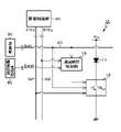
- FIG. 1 is a conceptual diagram of a circuit constituting the light emitting device according to the embodiment of the present disclosure.
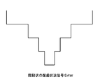
- FIG. 2 is a waveform diagram showing a stepped sawtooth wave signal SAW.
- FIG. 3 is a circuit diagram showing an example of the circuit configuration of the pixel circuit according to the first embodiment.
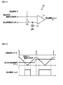
- FIG. 4A is a circuit diagram showing a circuit example of the light emission time control unit according to the reference example, and FIG. 4B is a waveform diagram for explaining an operation example of the light emission time control unit according to the reference example.
- FIG. 5A is a circuit diagram showing a circuit example of the light emission time control unit according to the second embodiment, and FIG. 5B is a waveform diagram for explaining an operation example of the light emission time control unit according to the second embodiment.
- FIG. 6A to 6D are diagrams showing how the light emission time is discretely controlled under the driving method according to the third embodiment.
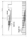
- FIG. 7 is a characteristic diagram showing a curve characteristic of current vs. luminance associated with discrete control of emission duty.
- FIG. 8 is a diagram illustrating the generation of a gamma curve with respect to the luminance gradation.
- FIG. 9A is a characteristic diagram of a logarithmic type luminance gamma characteristic
- FIG. 9B is a characteristic diagram of an arbitrary curve luminance gamma characteristic.
- FIG. 10A is a characteristic diagram of luminance vs. chromaticity without chromaticity correction by the driving method according to the fourth embodiment, and FIG.
- FIG. 10B is a luminance pair with chromaticity correction by the driving method according to the fourth embodiment. It is a characteristic diagram of chromaticity.
- FIG. 11 is a diagram illustrating chromaticity correction by the driving method according to the fourth embodiment.
- FIG. 12 is a circuit diagram showing a specific circuit example of the current modulation unit according to the fifth embodiment.
- 13A is a block diagram showing a specific circuit example of the sawtooth wave generation unit according to the sixth embodiment, and FIGS. 13B and 13C show an operation waveform example of the sawtooth wave generation unit according to the sixth embodiment. It is a waveform diagram.
- FIG. 14A is a waveform diagram of a sawtooth wave signal SAW when an extreme change in emission duty is accompanied between certain gradations, and FIG.
- FIG. 14B is a sawtooth wave signal for realizing the driving method according to the seventh embodiment. It is a waveform diagram of SAW.
- FIG. 15A is a diagram showing a scrolled image of a rectangular figure with a discrete change in emission duty
- FIG. 15B is a scrolled image of a lamp image with no discrete change in emission duty. It is a figure which shows.
- FIG. 16A is a diagram showing a scrolled image of a rectangular figure with a discrete change in emission duty
- FIG. 16B is a scrolled image of a rectangular figure with no discrete change in emission duty. It is a figure which shows.
- FIG. 17A is an operation explanatory diagram of the normal mode
- FIG. 17A is an operation explanatory diagram of the normal mode
- FIG. 17B is an operation explanatory diagram of the re-shooting mode according to the eighth embodiment.
- FIG. 18 is a timing waveform diagram showing the relationship between the exposure time of the rolling shutter and the light emission in the normal mode and the re-shooting mode.
- FIG. 19 is a circuit diagram showing an example of the circuit configuration of the pixel circuit according to the ninth embodiment.
- FIG. 20 is a circuit diagram showing a specific circuit example of the voltage modulation unit in the pixel circuit according to the ninth embodiment.
- FIG. 21 is a schematic view schematically showing a tiling display according to the first specific example of the electronic device of the present disclosure.
- FIG. 22 is an exploded perspective view schematically showing a liquid crystal display device according to a second specific example of the electronic device of the present disclosure.
- Example 2 Circuit example and operation example of the light emission time control unit in the pixel circuit according to the first embodiment
- Example 3 Example of a driving method for performing gradation control using the pixel circuit according to the first embodiment
- Example 4 Example of a driving method for correcting chromaticity in the current range used for gradation control
- Example 5 Specific circuit example of the current modulation unit in the pixel circuit according to the first embodiment
- Example 6 Specific circuit example and operating waveform example of sawtooth wave generator
- Example 7 (Example of a driving method that maintains good moving image characteristics when the emission duty is changed discretely) 2-9.
- Example 8 (Example having a re-shooting mode) 2-10.
- Example 9 (Circuit example of a pixel circuit in the case of voltage modulation) 3.
- Modification example 4 Electronic devices of the present disclosure 4-1.
- First specific example (example of tiling display) 4-2.
- Second specific example (example of a backlight device of a liquid crystal display device) 5. Configuration that can be taken by this disclosure
- the output transistor of the amplitude modulation unit is controlled on / off under the control of the gradation control unit for the light emitting time control unit.
- the emission time of the light emitting unit is controlled discretely by It can be configured to control the voltage value to be applied.
- the amplitude modulation unit may be configured to be a current modulation unit that controls the current value flowing through the light emitting unit or a voltage modulation unit that controls the voltage value applied to the light emitting unit.
- the driving method of the light emitting device, and the electronic device include a sawtooth wave generating unit that generates a stepped sawtooth wave signal, a light emitting time control unit is provided.
- the light emitting time of the light emitting unit can be controlled based on the stepped sawtooth wave signal generated by the sawtooth wave generating unit.
- a stepped sawtooth wave signal is generated for each pixel row of the pixel array unit in which the pixel circuits are arranged in a matrix, and for the light emission time control unit, the sawtooth wave generation unit generates a stepped sawtooth wave signal. Based on the generated stepped sawtooth wave signal, the light emitting time of the light emitting unit can be controlled for each pixel row.
- the sawtooth wave generation unit can be configured to generate a stepped sawtooth wave signal by a sample hold circuit.
- the gradation control unit has a configuration in which the light emitting time of the light emitting unit is discretely reduced by a constant ratio. can do. Further, the gradation control unit can be configured to control the light emission time of the light emitting unit and the current value flowing through the light emitting unit so that the current vs. luminance characteristic approaches the gamma characteristic of the logarithmic curve.
- the emission duty of the gradation control unit is set to a gradation that increases the brightness by ⁇ times with respect to an arbitrary gamma curve. It is possible to multiply by ⁇ and change the step interval of the amplitude gradation according to the gradation interval so as to be variable so that the amplitude gradation becomes ⁇ times at this interval.
- the driving method of the light emitting device, and the electronic device the gradation control unit is used when the light emitting time of the light emitting unit is controlled discretely.
- the rate of change of one light emission of the light emission duty during the light emission period in the frame can be set to a predetermined ratio or less.
- the driving method of the light emitting device, and the electronic device regarding the gradation control unit, the light emitting unit is specified except for the minimum light emitting time width of the light emitting unit. It is possible to use only the light emitting current range and perform chromaticity correction with a single color in a section of a specific current range of the light emitting unit. Further, the gradation control unit can be configured such that the chromaticity correction for a single color is performed by using the technique of interpolation processing, and the chromaticity correction for a single color is performed by interpolation processing for two or more current values. ..
- the driving method of the light emitting device, and the electronic device the light emission in one frame period is divided into a plurality of times, and the light emitting duty is not changed periodically. It can be configured to have a shooting mode. Further, the light emitting element of the light emitting unit may be configured to be a light emitting diode.
- the light emitting element of the light emitting unit may be in the form of a light emitting diode.
- the light emitting diode can be a light emitting diode having a well-known configuration and structure. That is, a light emitting diode having an optimum configuration and structure and manufactured from an appropriate material may be selected depending on the emission color of the light emitting diode.
- the light emitting unit composed of a red light emitting diode functions as a red light emitting sub-pixel (sub pixel)
- the light emitting unit composed of a green light emitting diode functions as a green light emitting sub pixel.
- a light emitting unit composed of a blue light emitting diode functions as a blue light emitting sub-pixel.
- FIG. 1 is a conceptual diagram of a circuit constituting the light emitting device according to the embodiment of the present disclosure.
- Light emitting device and pixels (more specifically, sub-pixels, the same shall apply hereinafter) according to the embodiment of the present disclosure (hereinafter, may be referred to as "the present embodiment"). It has a pixel array section 20 in which a plurality of pixel circuits 10 including the sections are arranged in a matrix (two-dimensional matrix shape) in the row direction and the column direction.
- the light emitting device is further arranged around the pixel array unit 20, and as peripheral driving units for driving a plurality of pixel circuits 10, for example, a scanning unit (scanning line driving unit) 30, gradation control.
- peripheral driving units for driving a plurality of pixel circuits 10 for example, a scanning unit (scanning line driving unit) 30, gradation control.
- a portion 40, a sawtooth wave generation portion 50, and the like are provided.
- the scanning unit 30 drives a plurality of pixel circuits 10 through scanning lines 61 1 to 61 m wired for each pixel row with respect to a pixel array of m rows and n columns arranged in a two-dimensional matrix.
- the gradation control unit 40 connects the pixel array of m rows and n columns to a plurality of pixel circuits 10 through two control lines 62 1 to 62 m and control lines 63 1 to 63 m wired for each pixel row. , Modulation signal (I-Sig / V-Sig) and emission time control signal (D-Sig) are supplied, and gradation control is performed for each pixel.
- Modulation signal I-Sig / V-Sig
- D-Sig emission time control signal
- the sawtooth wave generation unit 50 uses a sawtooth wave signal having the waveform shown in FIG. 2, that is, a sawtooth wave signal whose level changes stepwise (hereinafter referred to as “stepped sawtooth wave signal”) SAW. Generate.
- stepped sawtooth wave signal a sawtooth wave signal whose level changes stepwise
- this light emitting device is used as a display device for displaying an image
- a signal is written for each line (pixel line), and after the scanning line is started to emit light, the next Move to line signal writing. Therefore, in accordance with this operation, the sawtooth wave generation unit 50 supplies the generated stepped sawtooth wave signal SAW to each pixel circuit 10 of the pixel array unit 20 for each pixel row.
- the sawtooth wave signal of the waveform shown in FIG. 2 may be upside down.
- peripheral drive units such as the scanning unit (scanning line drive unit) 30, the gradation control unit 40, and the sawtooth wave generation unit 50 are provided on the same substrate as the pixel array unit 20. It may be provided outside the substrate.
- the light emitting device having the above configuration can be used as an LED display device in which the light emitting portion of the pixel circuit is composed of a light emitting diode, and the light emitting portion of the pixel circuit is an organic EL display device composed of an organic EL element. Can be used as.
- the amplitude modulation for controlling the brightness by changing the light emitting current of the light emitting portion of the pixel (sub pixel) current modulation and voltage modulation can be considered.
- the current modulation unit is used as the amplitude modulation unit
- the voltage modulation unit is used as the amplitude modulation unit.
- the first embodiment is a circuit example of the pixel circuit 10 in the case of current modulation.
- FIG. 3 shows an example of the circuit configuration of the pixel circuit 10 according to the first embodiment.
- the pixel circuit 10 has a circuit configuration including a light emitting unit 11, a current modulation unit 12, and a light emitting time control unit 13.
- a self-luminous element such as a light emitting diode (LED) or an organic EL element can be used.
- a light emitting diode (LED) is used as a light emitting element of the light emitting unit 11.
- the light emitting element of the light emitting unit 11, that is, the anode electrode of the light emitting diode is connected to the power supply line of the power supply voltage VDD .
- the light emitting diode has a so-called blue shift in which the spectrum shifts to the blue side depending on the current (light emitting current) flowing through the element, and the chromaticity fluctuates depending on the value of the light emitting current, or in a low current region. It is known that there is a large variation in brightness.
- the current modulation unit 12 has an output transistor TR out connected in series with the light emitting unit 11, and controls the current value flowing through the light emitting unit 11 according to the light emitting time of the light emitting unit 11.
- the output transistor TR out is composed of, for example, an N-channel field effect transistor, the drain electrode is connected to the anode electrode of the light emitting unit 11, and the source electrode is connected to the reference potential node (for example, ground).
- the current modulation unit 12 enters an operating state in response to a scanning signal Gate given from the scanning unit 30 via the scanning lines 61 (61 1 to 61 m ). Then, the current modulation unit 12 is a current value flowing through the light emitting unit 11 according to the current modulation signal I-Sig given as a modulation signal from the gradation control unit 40 via the control line 62 ( 621 to 62 m ). That is, the current value of the light emitting current of the light emitting diode is controlled.
- the light emission time control unit 13 emits light from the scanning unit 30 via the scanning line 61 (61 1 to 61 m ) and from the gradation control unit 40 via the control line 63 (63 1 to 63 m ).
- the time control signal D-Sig and the stepped sawtooth wave signal SAW are input from the sawtooth wave generation unit 50, respectively.
- the light emitting time control unit 13 controls the light emitting time of the light emitting unit 11 based on the stepped sawtooth wave signal SAW and the light emitting time control signal D-Sig by entering the operating state in response to the scanning signal Gate. ..
- the ratio of the light emission time in the period of one frame (one display frame), which is a display unit for displaying one image, that is, the light emission duty (Duty) is controlled.
- the light emission time control unit 13 controls the output transistor TR out of the current modulation unit 12 on / off under the control of the gradation control unit 40. Under the control of the light emitting time control unit 13, the output transistor TR out of the current modulation unit 12 selectively cuts off the current flowing through the light emitting unit 11. That is, the current modulation unit 12 has a mechanism for selectively cutting off the current flowing through the light emitting unit 11.
- the gradation control unit 40 performs gradation control (gradation expression) by controlling the current modulation unit 12 and the light emission time control unit 13. Specifically, the gradation control unit 40 discretely (steps) the light emission time of the light emission unit 11 at a constant ratio by controlling the on / off of the output transistor TR out of the current modulation unit 12 by the light emission time control unit 13. In addition to controlling the reduction, gradation expression is performed by controlling the current value flowing through the light emitting unit 11 by the current modulation unit 12 according to the light emitting time of the light emitting unit 11.
- the pixel circuit 10 has a configuration in which the light emission time is discretely determined for each pixel by on / off control of the output transistor TR out of the current modulation unit 12.
- the light emission time is roughly changed stepwise by the on / off control of the output transistor TR out , and the light emission time is set to the light emission time determined by the on / off control of the output transistor TR out .
- the current modulation can be performed finely, and the drive using only the current value in a specific range can be realized.
- the stepped sawtooth wave signal SAW shown in FIG. 2 is used to set the step of the stepped waveform to be larger than the noise level. By doing so, it is possible to control the light emission time with high accuracy even with a simple circuit configuration.
- the noise referred to here is a potential fluctuation caused by a power supply fluctuation when the light emitting unit 11 emits light, and the noise level differs depending on the circuit form of the pixel circuit 10.
- the switch element is arranged in the current path of the light emitting unit 11, and the switching control of the switch element and the modulation control of the current modulation unit 12 are performed under the control of the gradation control unit 40. It is possible to realize a pixel circuit that controls detailed gradation by current modulation while controlling the light emission time.
- a pixel circuit having a configuration in which a switch element is arranged in the current path of the light emitting unit 11 will be described as a pixel circuit according to a reference example.
- the pixel circuit according to the reference example by introducing discrete time amplitude modulation that can be changed only within a predetermined time width, the problem of vulnerable to variation and noise of the PWM circuit is solved, and in most sections.
- the current region to be used it is possible to avoid changes in the emission color and variations in the low current region due to the current value of the emission current.
- the switch element since the light emitting current flows through the switch element that cuts off the current, the power supply voltage rises due to the voltage across the switch element, and there is a problem that the power consumption increases by that amount. Further, when the switch element is composed of a field effect transistor or the like in order to suppress an increase in the power supply voltage, it is necessary to increase the element size, which is a disadvantageous circuit configuration from the viewpoint of reducing the circuit scale.
- an LED display device using a TFT Thin Film Transistor
- a micro LED display device using a CMOS back plane and a micro LED element are driven by a TFT or a minute CMOS element.
- TFT Thin Film Transistor
- problems such as a variation in brightness in a low current region and a change in chromaticity due to a light emitting current.
- a very large emission current is controlled with respect to the element size, and it is desired to reduce the circuit scale. Therefore, from the viewpoint of reducing the circuit scale, it is not preferable to use the pixel circuit according to the reference example.
- a small-scale circuit having a small signal without using a switch element which would have a relatively large element size for passing a light emitting current.
- the light emission time control unit 13 generates a signal for controlling the start and end of light emission of the light emission unit 11 based on the light emission time control signal D-Sig sent from the gradation control unit 40, and sends the signal to the current modulation unit 12.
- the light emitting time of the light emitting unit 11 can be controlled by the light emitting unit 11.
- Various circuit configurations can be considered for the light emission time control unit 13, but simply, a circuit configuration that generates a light emission period pulse that rises at the start of light emission and falls at the end of light emission can be considered. This emission period pulse signal may be generated a plurality of times during one frame period.
- FIG. 4A the simple circuit configuration shown in FIG. 4A is illustrated as a reference example as the light emission time control unit 13 that generates a light emission period pulse signal.
- a circuit example of the light emission time control unit 13 according to the reference example is shown in FIG. 4A, and a waveform diagram for explaining an operation example of the light emission time control unit 13 according to the reference example is shown in FIG. 4B.
- the emission time control unit 13 has a circuit configuration including a comparator 131, an N-channel field effect transistor 132, and a capacitive element 133.
- the sawtooth wave signal whose level changes linearly (hereinafter referred to as “linear sawtooth wave signal”) and the DC signal are compared by the comparator 131.
- a pulse in a section where a linear sawtooth wave signal is cut off by a DC signal is output as a light emission period pulse signal.
- the emission time control unit 13 is extremely vulnerable to noise and various fluctuations, and even if noise is added to the linear sawtooth wave signal, the temperature of the comparator 131 is slight.
- the emission period pulse signal also fluctuates due to characteristics and variations. Therefore, as the pixel circuit 10, it is necessary to lower the impedance of the wiring of the linear sawtooth wave signal to stabilize the waveform, or to use a comparator 131 having a small variation, and the circuit scale is large and complicated. It will be expensive.
- the second embodiment is a circuit example and an operation example of the light emission time control unit that can avoid the trouble of the light emission time control unit according to the reference example.
- FIG. 5A shows a circuit example of the light emission time control unit 13 according to the second embodiment
- FIG. 5B shows a waveform diagram for explaining an operation example of the light emission time control unit 13 according to the second embodiment.
- the light emission time control unit 13 according to the second embodiment includes a comparator 131, an N-channel field effect transistor 132, and a capacitive element 133, and the basic circuit configuration is described in the light emission time control unit according to the reference example. Same as the case, except in the following points. That is, in the light emission time control unit according to the reference example, the comparator 131 compares the linear sawtooth wave signal with the DC signal, whereas in the light emission time control unit 13 according to the second embodiment, the comparator 131 is used. However, there is a difference in comparing the stepped sawtooth wave signal shown in FIG. 2 with the DC signal.
- the emission time control unit 13 uses a stepped sawtooth wave signal instead of a linear sawtooth wave signal as the sawtooth wave signal, and limits the emission width that can be taken in advance. I try to keep it. As a result, noise up to the height of the staircase waveform of the stepped sawtooth wave signal is less likely to affect the emission width.
- the third embodiment is an example of a driving method (that is, a driving method of a light emitting device) for performing gradation control in the pixel circuit according to the first embodiment using a stepped sawtooth wave signal.
- a driving method that is, a driving method of a light emitting device
- the current value of the light emitting unit 11 is controlled by the current modulation unit 12 under the control by the gradation control unit 40, and the gradation control is performed. This is performed by on / off control of the output transistor TR out of the current modulation unit 12 by the light emission time control unit 13.
- the gradation control unit 40 controls to discretely reduce the light emission time of the light emitting unit 11 at a constant ratio. Specifically, when the current is reduced until the brightness of the light emitting unit 11 becomes a multiple ⁇ times smaller than the maximum value, the light emitting duty is multiplied by ⁇ in the next gradation to return the current to the maximum value. With this light emission duty, the current is reduced again, and when the brightness becomes ⁇ times, the light emission duty is multiplied by ⁇ again to return to the maximum value. By repeating this operation, the brightness can be reduced without changing the variable range of the current, and the most gradations can be obtained.
- the emission duty is set to a value larger than ⁇ times when the current is reduced until the brightness becomes ⁇ times, the current will not return to the maximum value when the next gradation is determined.
- the gradation intersects between each discrete emission duty. By alternately using the intersecting gradations for each frame, it can be used to alleviate the pseudo contour and the difference in chromaticity between each emission duty.
- FIGS. 6A to 6D show how the emission time is controlled discretely.
- the current vs. luminance characteristic can be made into a curve characteristic as shown in FIG. 7.
- the luminance range A to the luminance range D correspond to the light emission times of FIGS. 6A to 6D, respectively.
- the characteristic diagram shown in FIG. 7 illustrates the case of 2 bits and 4 steps.
- the luminance L (I 0 ) is given by the following equation, where I max is the maximum emission current value and I 0 is the emission current at which the luminance is ⁇ times larger.
- L (I 0 ) ⁇ ⁇ L (I max )
- the drive method according to the third embodiment by using the drive method according to the third embodiment, as shown in the characteristic diagram of FIG. 7, many luminance gradations are expressed using only a limited current section X.
- many luminance gradations can be expressed by using only a specific emission current range X other than the minimum emission time width of the light emitting unit 11.
- the influence of the chromaticity change of the light emitting unit 11 due to the light emitting current can be suppressed to a small value.
- the minimum emission time can be reduced to some extent, gradations below that can be expressed by error diffusion, which is one of the dithering methods. Therefore, use a low current region with large brightness variation. All gradations can be expressed without any need.
- the emission duty is multiplied by ⁇ and the current is returned to the maximum value.
- the brightness gamma characteristics in the form of a logarithmic curve that is, the logarithmic brightness gamma characteristics, as shown in FIG. 9A, can be realized. Can be done.
- the gradation control unit 40 controls the light emission duty of the light emitting unit 11 and the current value flowing through the light emitting unit 11 so that the current vs. luminance characteristic approaches the gamma characteristic of the logarithmic curve.
- the emission duty is multiplied by ⁇ at a gradation in which the luminance becomes ⁇ times for any gamma curve to be realized.
- the step interval of the amplitude gradation is changed according to the adjustment interval and the amplitude gradation is changed to be ⁇ times at this interval, the luminance gamma characteristic of an arbitrary gamma curve as shown in FIG. 9B is obtained. Can be realized.
- the luminance gamma characteristic in the form of a logarithmic curve shown in FIG. 9A is a very advantageous characteristic particularly in configuring a tiling display described later.
- a tiling display is a display device formed by arranging a plurality of display units (unit panels) in a tile shape. In this tiling display, if the adjacent display units do not have the same gamma characteristic, a luminance step will occur and the image quality will deteriorate, so that fine luminance adjustment is required.
- the luminance is changed at a constant small rate of change with respect to the brightness over the entire range of the emission current. Control is possible. Then, for example, if the luminance can be adjusted at a luminance ratio of about 1.8%, the luminance difference is less than the discrimination luminance difference of the human eye, so that there is no luminance step between adjacent display units, and the image quality is excellent. It is possible to configure a tiling display.
- the minimum value of the emission current is determined except for the minimum emission duty to lower the current value, and error diffusion is used for gradations lower than the minimum current in the minimum emission duty. It is very meaningful in terms of chromaticity change to express the gradation and use it so as to adjust the gradation with a current value equal to or higher than the minimum current value.
- the red light emitting diode has a small change in chromaticity due to the characteristics of the material, but the green and blue light emitting diodes have a large change in chromaticity. , The change in chromaticity can be suppressed to a small extent.
- the driving method according to the third embodiment the gradation performance is high without using as much as possible the low current region, which is resistant to noise and various fluctuations even with a simple circuit configuration and has many problems in driving the light emitting diode. It is possible to realize driving without chromaticity change.
- the fourth embodiment is an example of a driving method for performing chromaticity correction in the current range used for gradation control.
- gradation control using only a limited current range (current range X shown in FIG. 7) can be realized.
- the color difference in the current region that is repeatedly used is smaller than the color difference in the low current region, the light emitting unit 11, particularly the light emitting diode, is not without the influence of the blue shift of the spectrum due to the light emitting current.
- the chromaticity of the maximum working current is used as a reference, the chromaticity difference (color difference) at each gradation by the driving method according to the third embodiment changes jaggedly due to the current region used repeatedly, as shown in FIG. 10A. It ends up.
- the chromaticity correction with a single color is performed under the control of the gradation control unit 40.
- R (red) G (green) is a current value of two or more points, that is, the maximum current value and the minimum current value in the repeatedly used region in the current range X used for gradation control.
- Matrix chromaticity correction using other colors of B (blue) is performed. In this way, in the region between the maximum current value and the minimum repetitive current value, the characteristic diagram of the luminance-to-chromaticity difference in FIG.
- FIGS. 10A and 10B are performed by performing matrix linear chromaticity correction by linear interpolation of the matrix of the above two points. As shown in, it is possible to suppress the change in chromaticity due to the emission current at each gradation. That is, as is clear from the comparison between FIGS. 10A and 10B, it can be seen that almost strict chromaticity correction is possible according to the driving method according to the fourth embodiment.
- the fifth embodiment is a specific circuit example of the current modulation unit 12 in the pixel circuit 10 according to the first embodiment.
- FIG. 12 shows a specific circuit example of the current modulation unit 12 according to the fifth embodiment.
- the current modulation unit 12 has an N-channel field effect transistor 121, a capacitive element 122, and an N-channel field effect transistor, in addition to the output transistor TR out connected in series to the light emitting unit 11. It has a configuration having a CMOS inverter including 123 and a P-channel field effect transistor 124.
- the N-channel field effect transistor 121 is turned on by applying the scanning signal Gate to the gate electrode, writes the current modulation signal I-Sig, and is a capacitive element 122. Hold on. Then, when the light emission period pulse signal is input, the on / off control of the output transistor TR out is performed by the light emission period pulse signal.
- Example 6 is a specific circuit example and an operation waveform example of the sawtooth wave generation unit 50.
- a specific circuit example of the sawtooth wave generation unit 50 according to the sixth embodiment is shown in FIG. 13A, and an operation waveform example is shown in FIGS. 13B and 13C.
- the sawtooth wave generation unit 50 needs to generate a sawtooth wave signal SAW for each scanning line. Therefore, since the circuit portion that generates the sawtooth wave signal SAW is provided for each scanning line, it is desired to realize it with a simple circuit.
- the circuit shown in FIG. 13A is a circuit portion provided for each scanning line of the sawtooth wave generation unit 50. Since the sawtooth wave signal SAW to be generated by the sawtooth wave generation unit 50 has a stepped waveform as shown in FIG. 2, it can be realized by the sample hold circuit 51 that sample-holds the voltage.
- the sample hold circuit 51 is composed of, for example, two operational amplifiers 511 and 512, an N-channel field-effect transistor 513, a P-channel field-effect transistor 514, and two capacitive elements 515 and 516.
- the write signal shown in FIG. 13B and the variable voltage shown by the broken line in FIG. 13C are input to the sample hold circuit 51.
- the sample hold circuit 51 can generate the sawtooth wave signal SAW shown by the solid line in FIG. 13C by sample-holding the variable voltage in synchronization with the write signal.
- the variable voltage can be easily realized by using a source driver or the like used in an organic EL display device or the like.
- the seventh embodiment is an example of a driving method that maintains good moving image characteristics when the emission duty is changed discretely.
- the rate of change of one light emission of the light emission duty is preferable to suppress the rate of change of one light emission of the light emission duty to a predetermined ratio (for example, 75%) or less.
- a predetermined ratio for example, 75%) or less.
- the light emission is partially divided, and the rate of change of one light emission of the light emission duty during the light emission period within one frame is set to a predetermined ratio (one example) while maintaining the total light emission duty. That is, the change in time from the start of light emission to the end of light emission is reduced to 75%) or less so as not to be accompanied by an extreme change in light emission duty.
- FIG. 14A shows a waveform diagram of the sawtooth wave signal SAW when an extreme change in emission duty is accompanied between certain gradations.
- the waveform of FIG. 14A corresponds to the waveform of the stepped sawtooth wave signal SAW shown in FIG.
- FIG. 14B shows a waveform diagram of the sawtooth wave signal SAW for realizing the driving method according to the seventh embodiment.
- Both FIGS. 14A and 14B illustrate the waveform of the sawtooth wave signal SAW when the emission duty changes by 0.5 times.
- FIGS. 15A and 15B, and FIGS. 16A and 16B show the moving image simulation results of the 10 Pixel / Frame scroll image of the horizontal luminance lamp and the vertical bar-shaped vertical luminance lamp when the signal SAW is divided into two.
- the moving image simulation results of FIGS. 15A and 16A are simulation results in the case of FIG. 14A with one sawtooth wave signal SAW, that is, in the case of accompanied by discrete changes in emission duty, but the horizontal lamp image has a pseudo contour. It can be seen that the amount of blur is gradually changing in the vertical bar-shaped vertical lamp image.
- FIGS. 15B and 16B show the case of FIG. 14B in which the sawtooth wave signal SAW is divided into two under the driving by the driving method according to the seventh embodiment, that is, the case where the emission duty is not discretely changed. It is a simulation result of. According to the driving method according to the seventh embodiment, it can be seen that the pseudo contour is greatly improved and the amount of blurring is natural as compared with the case where the emission duty is accompanied by a discrete change.
- the switching point of the step of the sawtooth wave signal SAW is slightly changed for each frame, and the switching point of the emission duty is scattered for each frame to blur the depth of the pseudo contour and the switching point of the moving image blur.
- the method can be considered.
- reducing the time change from the start of light emission to the end of light emission and narrowing the light emission duty during the light emission period within one frame means inserting black. .. Then, by inserting black, it is possible to reduce the influence on the moving image blur (moving image distortion).
- Example 8 is an example having a re-shooting mode that realizes strong light emission for re-shooting.
- "Re-shooting" is, for example, taking an image displayed on a display device such as a large screen with an image pickup device such as a CMOS image sensor.
- CMOS image sensors use a rolling shutter and are exposed for each scanning line. Therefore, when an image displayed on a display device is taken (retaken), the display device is exposed during this exposure. If the light is not emitted, the part is not exposed and a black band or the like may appear in the photograph. In order to prevent this by PWM drive, it is sufficient to repeat blinking at short intervals for the light emission of the display device at equal time intervals.
- the display device has a re-shooting mode that realizes strong light emission for re-shooting, in addition to the normal mode that controls to change the light emitting duty discretely.
- the normal mode as shown in FIG. 17A, one frame period is divided into a writing section and a light emitting section, and the light emitting duty is discretely changed in the light emitting section.
- the re-shooting mode as shown in FIG. 17B, the light emission in one frame period is divided into a plurality of times, and the light emission duty is not changed periodically.
- the re-shooting mode in the display device according to the eighth embodiment since the light emitting unit 11 is in a state of constantly emitting light, it is possible to realize strong light emission for re-shooting and the embodiment. It is possible to suppress the occurrence of the moving image problem described in 4.
- FIG. 18 shows the relationship between the exposure time of the rolling shutter and the light emission in the normal mode and the re-shooting mode.
- the light emission in the normal mode with respect to the exposure time of the rolling shutter is shaded.
- Example 9 is a circuit example of the pixel circuit 10 in the case of voltage modulation.
- FIG. 19 shows an example of the circuit configuration of the pixel circuit 10 according to the ninth embodiment.
- the pixel circuit 10 has a circuit configuration including a light emitting unit 11, a voltage modulation unit 14, and a light emitting time control unit 13.
- a self-luminous element such as a light emitting diode (LED) or an organic EL element can be used as the light emitting element of the light emitting unit 11.
- FIG. 20 shows a specific circuit example of the voltage modulation unit 14.
- the voltage modulation unit 14 includes a CMOS inverter including an N-channel field-effect transistor 141, a capacitive element 142, an N-channel field-effect transistor 143 and a P-channel field-effect transistor 144, and an operational amplifier 145. It has become.
- the output transistor (not shown) of the operational amplifier 145 is connected in series with the light emitting unit 11.
- the N-channel field effect transistor 141 is turned on by applying the scanning signal Gate to the gate electrode, writes the voltage modulation signal V-Sig supplied from the gradation control unit 40, and writes the voltage modulation signal V-Sig to the capacitive element 142. Hold. Then, when the light emitting period pulse signal is input, the activation / deactivation of the operational amplifier 145 including the output transistor connected in series to the light emitting unit 11 is controlled by the light emitting period pulse signal. become.
- the pixel circuit 10 according to the ninth embodiment has a configuration in which the light emission time is discretely determined for each pixel by controlling the activation / deactivation of the operational amplifier 145 of the voltage modulation unit 14.
- the pixel circuit 10 according to the ninth embodiment of this configuration that is, the voltage-modulated pixel circuit 10, can also operate and have the same effect as the current-modulated pixel circuit 10. That is, the emission time is roughly changed stepwise by controlling the activation / deactivation of the operational amplifier 145, and the gradation control unit 40 adjusts to the emission time determined by the activation / deactivation control of the operational amplifier 145.
- the technique of the present disclosure has been described above based on the preferred embodiment, the technique of the present disclosure is not limited to the embodiment.
- the configuration and structure of the display device described in the above embodiment are examples, and can be changed as appropriate.
- a circuit configuration in which the light emitting unit 11 is arranged on the power supply voltage V DD side with respect to the current modulation unit 12 is exemplified.
- V DD side the power supply voltage
- the reference potential node for example, ground
- the display device of the present disclosure described above is a display unit (display device) of an electronic device in all fields that displays a video signal input to the electronic device or a video signal generated in the electronic device as an image or a video. Can be used as.
- Examples of the electronic devices of the present disclosure include television sets, notebook personal computers, digital still cameras, mobile terminal devices such as mobile phones, and tyling displays. However, it is not limited to these.
- the first specific example of the electronic device using the display device of the present disclosure is an example of a tiling display.
- FIG. 21 is a schematic view showing a tiling display according to a specific example of the electronic device of the present disclosure.
- the tiling display 100 is, for example, a display device formed by arranging a total of nine display units (unit panels) 101 of 3 ⁇ 3 in a tile shape.
- the number of display units 101 is 3 ⁇ 3, a total of 9, but the number of display units 101 is arbitrary.
- the light emitting device in which the current vs. luminance characteristic is the gamma characteristic of the logarithmic curve, is used as the display unit 101. This makes it possible to control the luminance with a constant small rate of change with respect to the luminance over the entire range of the emission current.
- the luminance difference is less than the discrimination luminance difference of the human eye, so that there is no luminance step between the adjacent display units 101, and the image quality is excellent. It will be possible to provide a tiling display.
- FIG. 22 is an exploded perspective view schematically showing a liquid crystal display device according to a second specific example of the electronic device of the present disclosure.
- the liquid crystal display device 200 according to the second specific example has a so-called direct LED partial drive configuration in which a backlight device 300 using a light emitting diode (LED) as a light emitting unit is arranged on the back surface.
- a backlight device 300 using a light emitting diode (LED) as a light emitting unit is arranged on the back surface.
- the light emitting device according to the above-described embodiment can be used.
- a liquid crystal display device having excellent image quality is obtained by performing partial drive in which only the light emitting unit (LED) of a bright scene is turned on and the light emitting unit (LED) is not turned on for a dark scene. It will be possible to provide.
- the present disclosure may also have the following configuration.
- a pixel circuit including a light emitting unit and Gradation control unit that controls gradation, Equipped with The pixel circuit is A light emitting time control unit that controls the light emitting time of the light emitting unit, and a light emitting unit.
- the light emitting time control unit discretically controls the light emitting time of the light emitting unit by controlling the output transistor of the amplitude modulation unit on / off under the control of the gradation control unit.
- the amplitude modulation unit controls the current value flowing through the light emitting unit or the voltage value applied to the light emitting unit according to the light emitting time of the light emitting unit under the control of the gradation control unit.
- the amplitude modulation unit is a current modulation unit that controls the current value flowing through the light emitting unit, or a voltage modulation unit that controls the voltage value applied to the light emitting unit.
- a sawtooth wave generator for generating a stepped sawtooth wave signal is provided.
- the light emitting time control unit controls the light emitting time of the light emitting unit based on the stepped sawtooth wave signal generated by the sawtooth wave generating unit.
- the light emitting device according to any one of the above [A-01] to the above [A-03].
- the sawtooth wave generation unit generates a stepped sawtooth wave signal for each pixel row of the pixel array unit in which pixel circuits are arranged in a matrix.
- the light emitting time control unit controls the light emitting time of the light emitting unit for each pixel row based on the stepped sawtooth wave signal generated by the sawtooth wave generation unit.
- the light emitting device according to the above [A-04].
- the sawtooth wave generator generates a stepped sawtooth wave signal by a sample hold circuit.
- the light emitting device according to the above [A-04] or the above [A-05].
- the gradation control unit discretely reduces the light emission time of the light emitting unit at a constant ratio.
- the light emitting device according to any one of the above [A-01] to the above [A-06].
- the gradation control unit controls the light emission time of the light emitting unit and the current value flowing through the light emitting unit so that the current vs. luminance characteristic approaches the gamma characteristic of the logarithmic curve.
- the light emitting device according to the above [A-07].
- the gradation control unit changes the emission duty by ⁇ for any gamma curve at a gradation that increases the brightness by ⁇ times, and allocates the step interval of the amplitude gradation according to this gradation interval. , The amplitude gradation is variable so that it is ⁇ times at this interval.
- the light emitting device according to the above [A-07].
- the gradation control unit sets the rate of change of one light emission of the light emission duty during the light emission period within one frame to a predetermined ratio or less when the light emission time of the light emitting unit is controlled discretely.
- the light emitting device according to any one of the above [A-02] to the above [A-09].
- the gradation control unit uses only a specific light emitting current range of the light emitting unit except for the minimum light emitting time width of the light emitting unit.
- the light emitting device according to any one of the above [A-02] to the above [A-10].
- the gradation control unit corrects the chromaticity with a single color in a section of a specific current range of the light emitting unit.
- the light emitting device according to the above [A-11].
- the gradation control unit performs chromaticity correction with a single color by using the technique of interpolation processing.
- the light emitting device according to the above [A-12].
- the gradation control unit performs chromaticity correction with a single color by interpolation processing of two or more current values.
- [A-15] It has a re-shooting mode in which light emission in one frame period is divided into a plurality of times and the light emission duty is not changed periodically.
- the light emitting element of the light emitting unit is a light emitting diode.
- a pixel circuit including a light emitting unit and Gradation control unit that controls gradation, Equipped with The pixel circuit is A light emitting time control unit that controls the light emitting time of the light emitting unit, and a light emitting unit.
- Amplitude modulator including an output transistor connected in series with the light emitting unit, In driving a light emitting device with Under the control of the gradation control unit, the output transistor of the amplitude modulation unit is turned on / off, and the gradation is controlled by controlling the modulation of the amplitude modulation unit. How to drive the light emitting device.
- [B-02] The light emitting time of the light emitting unit is controlled based on the stepped sawtooth wave signal.
- [B-03] The light emitting time of the light emitting unit is controlled for each pixel row based on the stepped sawtooth wave signal.
- [B-04] The emission time of the light emitting unit is discretely reduced by a constant ratio.
- [B-05] The light emitting time of the light emitting unit and the current value flowing through the light emitting unit are controlled so that the current vs.
- [B-07] The rate of change of one light emission of the light emission duty in one light emission period when the light emission time of the light emitting unit is controlled discretely is set to a predetermined ratio or less.
- [B-08] Except for the minimum emission time width of the light emitting unit, only a specific emission current range of the light emitting unit is used.
- [B-09] Performs chromaticity correction with a single color in a section of a specific current range of the light emitting unit.
- [B-10] The chromaticity correction with a single color is performed by using the technique of interpolation processing.
- [B-11] The chromaticity correction for a single color is performed by interpolation processing of current values of two or more points.
- [B-12] It has a re-shooting mode in which light emission in one frame period is divided into a plurality of times and the light emission duty is not changed periodically.
- [B-13] The light emitting element of the light emitting unit is a light emitting diode.
- Pixel circuit including a light emitting unit and Gradation control unit that controls gradation, Equipped with The pixel circuit is A light emitting time control unit that controls the light emitting time of the light emitting unit, and a light emitting unit.
- Amplitude modulator including an output transistor connected in series with the light emitting unit, Have, The gradation control unit performs gradation control by performing on / off control of the output transistor of the amplitude modulation unit and modulation control of the amplitude modulation unit via the light emission time control unit.
- An electronic device having a light emitting device.
- the light emitting time control unit discretically controls the light emitting time of the light emitting unit by controlling the output transistor of the amplitude modulation unit on / off under the control of the gradation control unit.
- the amplitude modulation unit controls the current value flowing through the light emitting unit or the voltage value applied to the light emitting unit according to the light emitting time of the light emitting unit under the control of the gradation control unit.
- the amplitude modulation unit is a current modulation unit that controls the current value flowing through the light emitting unit, or a voltage modulation unit that controls the voltage value applied to the light emitting unit.
- a sawtooth wave generator for generating a stepped sawtooth wave signal is provided.
- the light emitting time control unit controls the light emitting time of the light emitting unit based on the stepped sawtooth wave signal generated by the sawtooth wave generating unit.
- the electronic device according to any one of the above [C-01] to the above [C-03].
- the sawtooth wave generation unit generates a stepped sawtooth wave signal for each pixel row of the pixel array unit in which pixel circuits are arranged in a matrix.
- the light emitting time control unit controls the light emitting time of the light emitting unit for each pixel row based on the stepped sawtooth wave signal generated by the sawtooth wave generation unit.
- the electronic device according to the above [C-04].
- the sawtooth wave generator generates a stepped sawtooth wave signal by a sample hold circuit.
- the gradation control unit discretely reduces the light emission time of the light emitting unit at a constant ratio.
- the gradation control unit controls the light emission time of the light emitting unit and the current value flowing through the light emitting unit so that the current vs. luminance characteristic approaches the gamma characteristic of the logarithmic curve.
- the gradation control unit changes the emission duty by ⁇ for any gamma curve at a gradation that increases the brightness by ⁇ times, and allocates the step interval of the amplitude gradation according to this gradation interval. , The amplitude gradation is variable so that it is ⁇ times at this interval.
- the electronic device according to the above [C-07].
- the gradation control unit sets the rate of change of one light emission of the light emission duty during the light emission period within one frame to a predetermined ratio or less when the light emission time of the light emitting unit is controlled discretely.
- the electronic device uses only a specific light emitting current range of the light emitting unit except for the minimum light emitting time width of the light emitting unit.
- the electronic device according to any one of the above [C-02] to the above [C-10].
- the gradation control unit corrects the chromaticity with a single color in a section of a specific current range of the light emitting unit.
- the electronic device according to the above [C-11].
- [C-13] The gradation control unit performs chromaticity correction with a single color using the technique of interpolation processing.
- the electronic device according to the above [C-12].
- the gradation control unit performs chromaticity correction with a single color by interpolation processing of two or more current values.
- [C-15] It has a re-shooting mode in which light emission in one frame period is divided into a plurality of times and the light emission duty is not changed periodically.
- the light emitting element of the light emitting unit is a light emitting diode.
Landscapes
- Engineering & Computer Science (AREA)
- Physics & Mathematics (AREA)
- Computer Hardware Design (AREA)
- General Physics & Mathematics (AREA)
- Theoretical Computer Science (AREA)
- Control Of Indicators Other Than Cathode Ray Tubes (AREA)
Priority Applications (3)
| Application Number | Priority Date | Filing Date | Title |
|---|---|---|---|
| CN202180074415.1A CN116457863A (zh) | 2020-11-10 | 2021-10-04 | 发光装置、发光装置的驱动方法以及电子设备 |
| US18/251,347 US12125441B2 (en) | 2020-11-10 | 2021-10-04 | Light-emitting device, method of driving light- emitting device, and electronic apparatus |
| JP2022561323A JP7782457B2 (ja) | 2020-11-10 | 2021-10-04 | 発光装置、発光装置の駆動方法、及び、電子機器 |
Applications Claiming Priority (2)
| Application Number | Priority Date | Filing Date | Title |
|---|---|---|---|
| JP2020187090 | 2020-11-10 | ||
| JP2020-187090 | 2020-11-10 |
Publications (1)
| Publication Number | Publication Date |
|---|---|
| WO2022102282A1 true WO2022102282A1 (ja) | 2022-05-19 |
Family
ID=81600953
Family Applications (1)
| Application Number | Title | Priority Date | Filing Date |
|---|---|---|---|
| PCT/JP2021/036671 Ceased WO2022102282A1 (ja) | 2020-11-10 | 2021-10-04 | 発光装置、発光装置の駆動方法、及び、電子機器 |
Country Status (4)
| Country | Link |
|---|---|
| US (1) | US12125441B2 (https=) |
| JP (1) | JP7782457B2 (https=) |
| CN (1) | CN116457863A (https=) |
| WO (1) | WO2022102282A1 (https=) |
Families Citing this family (1)
| Publication number | Priority date | Publication date | Assignee | Title |
|---|---|---|---|---|
| KR102622413B1 (ko) * | 2022-03-03 | 2024-01-08 | 주식회사 글로벌테크놀로지 | 디스플레이를 위한 백라이트 장치 및 그의 전류 제어 집적회로 |
Citations (4)
| Publication number | Priority date | Publication date | Assignee | Title |
|---|---|---|---|---|
| JP2011070184A (ja) * | 2009-09-09 | 2011-04-07 | Ignis Innovation Inc | アクティブマトリクス・ディスプレイ用の駆動システム |
| WO2018164105A1 (ja) * | 2017-03-06 | 2018-09-13 | ソニーセミコンダクタソリューションズ株式会社 | 駆動装置および表示装置 |
| US20180293929A1 (en) * | 2017-04-11 | 2018-10-11 | Samsung Electronics Co., Ltd. | Pixel circuit of display panel and display device |
| WO2019220265A1 (ja) * | 2018-05-17 | 2019-11-21 | 株式会社半導体エネルギー研究所 | 表示パネル、表示装置、入出力装置、情報処理装置 |
Family Cites Families (22)
| Publication number | Priority date | Publication date | Assignee | Title |
|---|---|---|---|---|
| US5956004A (en) * | 1993-05-11 | 1999-09-21 | Micron Technology, Inc. | Controlling pixel brightness in a field emission display using circuits for sampling and discharging |
| JPH09101760A (ja) * | 1995-10-04 | 1997-04-15 | Pioneer Electron Corp | 発光素子の駆動方法および駆動装置 |
| JP4453136B2 (ja) * | 1999-12-15 | 2010-04-21 | 日本ビクター株式会社 | マトリクス型画像表示装置 |
| JP3868826B2 (ja) * | 2002-02-25 | 2007-01-17 | シャープ株式会社 | 画像表示装置の駆動方法および画像表示装置の駆動装置 |
| JP3742093B2 (ja) * | 2004-02-19 | 2006-02-01 | シャープ株式会社 | 映像表示装置 |
| JP2007323036A (ja) * | 2006-06-05 | 2007-12-13 | Samsung Sdi Co Ltd | 有機電界発光表示装置及びその駆動方法 |
| JP2007333768A (ja) | 2006-06-12 | 2007-12-27 | Sony Corp | ディスプレイ装置及びディスプレイ装置の駆動方法 |
| EP2239723B1 (en) * | 2008-02-08 | 2015-01-28 | Sharp Kabushiki Kaisha | Pixel circuit and display device |
| JP2010243775A (ja) * | 2009-04-06 | 2010-10-28 | Canon Inc | 補正値の取得方法、補正方法、画像表示装置 |
| JP5351973B2 (ja) * | 2009-10-29 | 2013-11-27 | シャープ株式会社 | 画素回路及び表示装置 |
| US8947418B2 (en) * | 2010-11-25 | 2015-02-03 | Sharp Kabushiki Kaisha | Display device |
| JP5625864B2 (ja) * | 2010-12-15 | 2014-11-19 | ソニー株式会社 | 表示装置及び表示装置の駆動方法 |
| JP5880467B2 (ja) * | 2013-02-04 | 2016-03-09 | ソニー株式会社 | コンパレータ装置、並びに、表示装置及びその駆動方法 |
| JP2015004945A (ja) * | 2013-02-04 | 2015-01-08 | ソニー株式会社 | 表示装置及びその駆動方法、並びに、制御パルス生成装置 |
| JP6157178B2 (ja) * | 2013-04-01 | 2017-07-05 | ソニーセミコンダクタソリューションズ株式会社 | 表示装置 |
| JP6129318B2 (ja) * | 2013-07-30 | 2017-05-17 | シャープ株式会社 | 表示装置およびその駆動方法 |
| JP2016212239A (ja) * | 2015-05-08 | 2016-12-15 | ソニー株式会社 | 表示装置、表示方法、および電子機器 |
| JP2021523407A (ja) * | 2018-05-08 | 2021-09-02 | アップル インコーポレイテッドApple Inc. | 画素内メモリディスプレイ |
| KR102538484B1 (ko) * | 2018-10-04 | 2023-06-01 | 삼성전자주식회사 | 디스플레이 패널 및 디스플레이 패널의 구동 방법 |
| KR102538488B1 (ko) * | 2018-10-04 | 2023-06-01 | 삼성전자주식회사 | 디스플레이 패널 및 디스플레이 패널의 구동 방법 |
| US11100840B2 (en) * | 2019-03-29 | 2021-08-24 | Samsung Electronics Co., Ltd. | Display panel and driving method of the display panel |
| EP3754639B1 (en) * | 2019-06-17 | 2023-09-27 | Samsung Electronics Co., Ltd. | Display module and driving method thereof |
-
2021
- 2021-10-04 US US18/251,347 patent/US12125441B2/en active Active
- 2021-10-04 WO PCT/JP2021/036671 patent/WO2022102282A1/ja not_active Ceased
- 2021-10-04 JP JP2022561323A patent/JP7782457B2/ja active Active
- 2021-10-04 CN CN202180074415.1A patent/CN116457863A/zh active Pending
Patent Citations (4)
| Publication number | Priority date | Publication date | Assignee | Title |
|---|---|---|---|---|
| JP2011070184A (ja) * | 2009-09-09 | 2011-04-07 | Ignis Innovation Inc | アクティブマトリクス・ディスプレイ用の駆動システム |
| WO2018164105A1 (ja) * | 2017-03-06 | 2018-09-13 | ソニーセミコンダクタソリューションズ株式会社 | 駆動装置および表示装置 |
| US20180293929A1 (en) * | 2017-04-11 | 2018-10-11 | Samsung Electronics Co., Ltd. | Pixel circuit of display panel and display device |
| WO2019220265A1 (ja) * | 2018-05-17 | 2019-11-21 | 株式会社半導体エネルギー研究所 | 表示パネル、表示装置、入出力装置、情報処理装置 |
Also Published As
| Publication number | Publication date |
|---|---|
| US12125441B2 (en) | 2024-10-22 |
| JPWO2022102282A1 (https=) | 2022-05-19 |
| JP7782457B2 (ja) | 2025-12-09 |
| US20240005861A1 (en) | 2024-01-04 |
| CN116457863A (zh) | 2023-07-18 |
Similar Documents
| Publication | Publication Date | Title |
|---|---|---|
| CN107735832B (zh) | 显示面板的发光控制装置和方法 | |
| US11651720B2 (en) | Display device, method of driving display device, and electronic apparatus | |
| US8497885B2 (en) | Display apparatus and drive method thereof | |
| CN109215564B (zh) | 显示面板的控制装置、显示装置以及显示面板的驱动方法 | |
| US9288403B2 (en) | Image processing circuit, image processing method, and display device | |
| JP4720757B2 (ja) | 光源装置および液晶表示装置 | |
| US20140225939A1 (en) | Display device and electronic device | |
| US10229642B2 (en) | Liquid crystal display device | |
| JP2015225150A (ja) | 表示装置及び電子機器 | |
| CN111739464A (zh) | 一种像素驱动电路、显示阵列及其驱动控制方法 | |
| CN1449129A (zh) | 光发射器 | |
| JP2012194256A (ja) | 表示装置および電子機器 | |
| JP2007503610A (ja) | 表示装置 | |
| WO2018036085A1 (zh) | 一种oled pwm数字驱动方法及电路 | |
| WO2022059606A1 (ja) | 表示装置、表示装置の駆動方法、及び、電子機器 | |
| CN110534054B (zh) | 显示驱动方法及装置、显示装置、存储介质、芯片 | |
| CN104464591A (zh) | 图像信号处理电路、图像信号处理方法以及显示装置 | |
| WO2022102282A1 (ja) | 発光装置、発光装置の駆動方法、及び、電子機器 | |
| JP4569107B2 (ja) | 表示装置及び表示装置の駆動方法 | |
| CN116057618B (zh) | 用于调光显示器的装置、系统和方法 | |
| JP5207685B2 (ja) | 表示装置及びその駆動方法 | |
| JP2009063654A (ja) | 表示装置及びその駆動方法 | |
| CN115885337A (zh) | 显示设备、显示设备的驱动方法和电子装置 | |
| HK40092950B (zh) | 用於调光显示器的装置、系统和方法 | |
| HK40092950A (zh) | 用於调光显示器的装置、系统和方法 |
Legal Events
| Date | Code | Title | Description |
|---|---|---|---|
| 121 | Ep: the epo has been informed by wipo that ep was designated in this application |
Ref document number: 21891529 Country of ref document: EP Kind code of ref document: A1 |
|
| ENP | Entry into the national phase |
Ref document number: 2022561323 Country of ref document: JP Kind code of ref document: A |
|
| WWE | Wipo information: entry into national phase |
Ref document number: 202180074415.1 Country of ref document: CN |
|
| WWE | Wipo information: entry into national phase |
Ref document number: 18251347 Country of ref document: US |
|
| NENP | Non-entry into the national phase |
Ref country code: DE |
|
| 122 | Ep: pct application non-entry in european phase |
Ref document number: 21891529 Country of ref document: EP Kind code of ref document: A1 |