WO2022097533A1 - 放電回路モジュール - Google Patents
放電回路モジュール Download PDFInfo
- Publication number
- WO2022097533A1 WO2022097533A1 PCT/JP2021/039425 JP2021039425W WO2022097533A1 WO 2022097533 A1 WO2022097533 A1 WO 2022097533A1 JP 2021039425 W JP2021039425 W JP 2021039425W WO 2022097533 A1 WO2022097533 A1 WO 2022097533A1
- Authority
- WO
- WIPO (PCT)
- Prior art keywords
- circuit module
- discharge circuit
- wiring
- discharge
- wiring portion
- Prior art date
- Legal status (The legal status is an assumption and is not a legal conclusion. Google has not performed a legal analysis and makes no representation as to the accuracy of the status listed.)
- Ceased
Links
Images



Classifications
-
- H—ELECTRICITY
- H10—SEMICONDUCTOR DEVICES; ELECTRIC SOLID-STATE DEVICES NOT OTHERWISE PROVIDED FOR
- H10W—GENERIC PACKAGES, INTERCONNECTIONS, CONNECTORS OR OTHER CONSTRUCTIONAL DETAILS OF DEVICES COVERED BY CLASS H10
- H10W76/00—Containers; Fillings or auxiliary members therefor; Seals
- H10W76/10—Containers or parts thereof
- H10W76/12—Containers or parts thereof characterised by their shape
- H10W76/15—Containers comprising an insulating or insulated base
- H10W76/157—Containers comprising an insulating or insulated base having interconnections parallel to the insulating or insulated base
-
- H—ELECTRICITY
- H10—SEMICONDUCTOR DEVICES; ELECTRIC SOLID-STATE DEVICES NOT OTHERWISE PROVIDED FOR
- H10W—GENERIC PACKAGES, INTERCONNECTIONS, CONNECTORS OR OTHER CONSTRUCTIONAL DETAILS OF DEVICES COVERED BY CLASS H10
- H10W90/00—Package configurations
-
- H—ELECTRICITY
- H10—SEMICONDUCTOR DEVICES; ELECTRIC SOLID-STATE DEVICES NOT OTHERWISE PROVIDED FOR
- H10W—GENERIC PACKAGES, INTERCONNECTIONS, CONNECTORS OR OTHER CONSTRUCTIONAL DETAILS OF DEVICES COVERED BY CLASS H10
- H10W40/00—Arrangements for thermal protection or thermal control
- H10W40/20—Arrangements for cooling
- H10W40/25—Arrangements for cooling characterised by their materials
- H10W40/255—Arrangements for cooling characterised by their materials having a laminate or multilayered structure, e.g. direct bond copper [DBC] ceramic substrates
-
- H—ELECTRICITY
- H10—SEMICONDUCTOR DEVICES; ELECTRIC SOLID-STATE DEVICES NOT OTHERWISE PROVIDED FOR
- H10W—GENERIC PACKAGES, INTERCONNECTIONS, CONNECTORS OR OTHER CONSTRUCTIONAL DETAILS OF DEVICES COVERED BY CLASS H10
- H10W72/00—Interconnections or connectors in packages
- H10W72/50—Bond wires
- H10W72/551—Materials of bond wires
- H10W72/552—Materials of bond wires comprising metals or metalloids, e.g. silver
- H10W72/5524—Materials of bond wires comprising metals or metalloids, e.g. silver comprising aluminium [Al]
-
- H—ELECTRICITY
- H10—SEMICONDUCTOR DEVICES; ELECTRIC SOLID-STATE DEVICES NOT OTHERWISE PROVIDED FOR
- H10W—GENERIC PACKAGES, INTERCONNECTIONS, CONNECTORS OR OTHER CONSTRUCTIONAL DETAILS OF DEVICES COVERED BY CLASS H10
- H10W90/00—Package configurations
- H10W90/701—Package configurations characterised by the relative positions of pads or connectors relative to package parts
- H10W90/751—Package configurations characterised by the relative positions of pads or connectors relative to package parts of bond wires
- H10W90/754—Package configurations characterised by the relative positions of pads or connectors relative to package parts of bond wires between a chip and a stacked insulating package substrate, interposer or RDL
Definitions
- This disclosure relates to a discharge circuit module.
- an X capacitor which is a capacitor connected between power supply lines.
- a discharge circuit for discharging the X capacitor is often provided.
- Some such discharge circuits have a configuration in which a resistor and a switch are connected in series (for example, Patent Document 1). This series-connected configuration is connected in parallel with the X capacitor. By turning on the switch, the electric charge stored in the X capacitor is discharged through the resistor.
- a ceramic resistor or a chip resistor arranged on a substrate may be used, and in that case, there is a risk that the discharge circuit becomes large.
- the present disclosure aims to provide a discharge circuit module that enables miniaturization.
- the discharge circuit module is a discharge circuit module for discharging a capacitive portion, and includes an insulating substrate, a discharge resistance portion having at least one resistor formed on the insulating substrate, and a discharge resistance portion. It has a semiconductor chip as a semiconductor switch mounted on the insulating substrate and electrically connected to the discharge resistance portion, and has a configuration in which the insulating substrate, the discharge resistance portion, and the semiconductor chip are packaged. ..
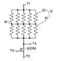
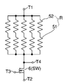
- FIG. 1 It is a figure which shows the circuit structure of the discharge system which concerns on the exemplary embodiment of this disclosure. It is an exploded perspective view of a discharge circuit module. It is a perspective view of the assembled state of a discharge circuit module. It is a circuit diagram which shows the structure of the discharge circuit in a discharge circuit module. It is a circuit diagram which shows the structure of the discharge circuit which concerns on one modification. It is a circuit diagram which shows the structure of the discharge resistance part which concerns on one modification. It is a schematic perspective view of the discharge circuit module which concerns on one modification.
- FIG. 1 is a diagram showing a circuit configuration of a discharge system 15 according to an exemplary embodiment of the present disclosure.
- the discharge system 15 shown in FIG. 1 has a capacitance unit CX composed of a plurality of capacitors and a discharge circuit module 1.
- the capacitance part CX corresponds to an X capacitor connected between the lines of the power supply line.
- the capacitance portion CX is formed by connecting five series configurations in which two capacitors are connected in series between the positive electrode side and the negative electrode side of the battery 10 in parallel.
- the capacitance portion CX may be formed from one capacitor connected between the positive electrode side and the negative electrode side of the battery 10.
- the discharge circuit module 1 is a package of a discharge circuit as described later, and has a discharge resistance unit R and a semiconductor switch SW.
- the discharge resistance unit R is composed of a plurality of resistors. Not limited to this, the discharge resistance unit R may be composed of one resistor.
- the semiconductor switch SW is composed of a SiC- MOSFET (Metal-Oxide-Semiconductor Field Effect Transistor) using SiC (silicon carbide) as a semiconductor material.
- the semiconductor switch SW may be composed of, for example, a Si- MOSFET or a Si-IGBT (Insulated Gate Bipolar Transistor).
- the semiconductor switch SW is an N-channel MOSFET.
- One end of the discharge resistance portion R is connected to the positive electrode side of the battery 10 (capacity portion CX).
- the other end of the discharge resistance portion R is connected to the first end of the semiconductor switch SW.
- the second end of the semiconductor switch SW is connected to the negative electrode side of the battery 10 (capacity portion CX).
- the semiconductor switch SW is composed of an N-channel MOSFET, the first end corresponds to a drain and the second end corresponds to a source.
- the on / off of the semiconductor switch SW is controlled by the control voltage applied to the control end (gate) of the semiconductor switch SW. If the semiconductor switch SW is turned on with the electric charge stored in the capacitance section CX, the discharge current flows through the discharge resistance section R and the semiconductor switch SW, so that the charge stored in the capacitance section CX is discharged.
- the DC voltage of the capacitance unit CX becomes a high voltage such as 600V to 900V.
- a high withstand voltage product such as 1200 V withstand voltage is used.
- the resistance value of the discharge resistance unit R is determined by a time constant for reducing the voltage of the capacitance unit CX to a predetermined voltage (for example, 45 V) or less after a predetermined time (for example, 2 sec) has elapsed from the start of discharge. Determined by the standard.
- the resistance value of the discharge resistance portion R is, for example, several tens of ⁇ .
- FIG. 2 is an exploded perspective view of the discharge circuit module 1.
- FIG. 3 is a perspective view of the discharged circuit module 1 in an assembled state. In FIG. 3, the cover 8 is not shown for convenience.
- the longitudinal direction (first direction) is shown as the X direction
- one side in the longitudinal direction is shown as X1
- the other side in the longitudinal direction is shown as X2.
- the short direction (second direction) is shown as the Y direction
- one side in the short direction is shown as Y1
- the other side in the short direction is shown as Y2.
- the vertical direction is shown as the Z direction
- the upper side is shown as Z1
- the lower side is shown as Z2.
- the longitudinal, lateral, and vertical directions are orthogonal to each other.
- the discharge circuit module 1 includes a copper plate 2, a solder portion 3, a DCB substrate 4, a first resistor group 51, a second resistor group 52, and a semiconductor chip 6. It has a resin case 7 and a cover 8. Further, the discharge circuit module 1 has external terminals T1 to T4 for establishing an electrical connection with the outside.
- the copper plate 2 is a copper plate-like member that extends in the longitudinal direction and the lateral direction, is substantially rectangular in the top view, and has the vertical direction as the thickness direction.
- the copper plate 2 has excellent thermal conductivity.
- a metal plate made of a metal other than copper having excellent thermal conductivity such as aluminum may be used.
- the resin case 7 is a housing made of resin. Instead of the resin case 7, a housing made of an insulating material other than the resin may be used.
- the resin case 7 integrally has a first mounting base portion 71, a second mounting base portion 72, a first piece portion 73, and a second piece portion 74.
- the first piece 73 and the second piece 74 are substantially wall-shaped members extending in the longitudinal direction, respectively.
- the first piece 73 and the second piece 74 are arranged so as to face each other in the lateral direction.
- the first mounting base 71 is arranged on the other side in the longitudinal direction, and the second mounting base 72 is arranged on one side in the longitudinal direction.
- the external terminal T1 is mounted on the first mounting table portion 71, and the external terminal T2 is mounted on the second mounting table portion 72.
- the first piece 73 and the second piece 74 connect the first mounting base 71 and the second mounting base 72 in the longitudinal direction, respectively.
- a storage portion S Surrounded by the first mounting base portion 71, the second mounting base portion 72, the first piece portion 73, and the second piece portion 74, a storage portion S, which is a space that opens up and down, is formed inside the resin case 7. Will be done.
- Fixing holes 7A penetrating in the vertical direction are formed at the four corners of the resin case 7 when viewed from above.
- through holes 2A penetrating in the vertical direction are formed at the four corners in the top view.
- the copper plate 2 is arranged below the resin case 7, and in that state, each through hole portion 2A and each fixing hole portion 7A overlap each other in a top view to form one through hole.
- a heat sink (not shown) can be fixed below the copper plate 2 by bolts (not shown) inserted in the vertical direction into each set including each through hole portion 2A and each fixing hole portion 7A.
- the heat sink is, for example, a water-cooled heat sink.
- the DCB (Direct Copper Bonding) substrate 4 is a plate-shaped member that extends in the longitudinal direction and the lateral direction and has the vertical direction as the thickness direction.
- the DCB substrate 4 includes a ceramic substrate 40, a first wiring portion 41, a second wiring portion 42, and a third wiring portion 43.
- the DCB substrate 4 is formed by directly joining the first wiring portion 41, the second wiring portion 42, and the third wiring portion 43, which are copper plates, to the ceramic substrate 40, respectively.
- the ceramic substrate 40 is formed of, for example, alumina, aluminum nitride, silicon nitride, etc., and has excellent thermal conductivity.
- the ceramic substrate 40 is an example of an insulating substrate.
- the first wiring portion 41, the second wiring portion 42, and the third wiring portion 43 are arranged in this order.
- the first wiring unit 41, the second wiring unit 42, and the third wiring unit 43 extend in the lateral direction.
- the first resistor group 51 is formed by printing on the ceramic substrate 40 so as to connect the first wiring portion 41 and the second wiring portion 42.
- the first resistor group 51 is composed of five resistors extending in the longitudinal direction and arranged in the lateral direction as an example.
- the second resistor group 52 is formed by printing on the ceramic substrate 40 so as to connect the second wiring portion 42 and the third wiring portion 43.
- the second resistor group 52 is composed of five resistors extending in the longitudinal direction and arranged in the lateral direction as an example.
- Each of the resistors constituting the first resistor group 51 and the second resistor group 52 is, for example, silver which is a metal, silver / palladium (Ag / Pd), or ruthenium oxide (RuO 2 ) which is a metal oxide. ) And so on.
- FIG. 4 is a circuit diagram showing the configuration of the discharge circuit in the discharge circuit module 1. As shown in FIG. 4, the discharge resistance unit R is composed of two series and five parallel connections of resistors as an example.
- each connection node N in each series connection configuration of the resistor is short-circuited by the second wiring portion 42.
- the connection of one resistor with the second wiring section 42 is disconnected for some reason in the series connection configuration of the resistors, the connection of the other resistor with the second wiring section 42 remains valid. Therefore, it is possible to suppress a change in the resistance value of the discharge resistance portion R.
- the DCB substrate 4 is arranged above the copper plate 2.
- the solder portion 3 is arranged so as to be sandwiched in the vertical direction by the DCB substrate 4 and the copper plate 2.
- the DCB substrate 4 is joined to the upper surface of the copper plate 2 via the solder portion 3.
- the DCB substrate 4, the first resistor group 51, and the second resistor group 52 are housed in the accommodating portion S.
- the external terminal T1 integrally has a mounting portion T1A and a leg portion T1B.
- the mounting portion T1A is a plate-shaped portion mounted on the first mounting base portion 71.
- the leg portion T1B is connected from the mounting portion T1A to a portion passed through the inside of the first mounting base portion 71, and is formed so as to project from the lower portion on one side in the longitudinal direction of the first mounting base portion 71 toward the accommodating portion S. ..
- the leg portion T1B is formed so as to extend from the first mounting base portion 71 in the order of one side in the longitudinal direction, the lower side, and one side in the longitudinal direction.
- the external terminal T1 is made of copper as an example. As described above, the third wiring portion 43 formed on the ceramic substrate 40 is electrically connected to the external terminal T1 by coming into contact with the leg portion T1B from below. That is, the third wiring portion 43 is connected to the external terminal T1 by the Cu clip.
- the semiconductor chip 6 corresponds to the semiconductor switch SW (FIG. 4).
- the lower surface of the semiconductor chip 6 is joined to the upper surface of the first wiring portion 41 by a solder portion (not shown).
- the external terminal T4 has a portion protruding upward from the upper surface of the second piece portion 74.
- the upper surface of the first wiring portion 41 is connected to the lower end portion of the external terminal T4 by the first bonding wire W1 (FIG. 3).
- the first bonding wire W1 is formed of, for example, aluminum.
- the semiconductor chip 6 semiconductor switch SW
- the drain of the semiconductor chip 6 is electrically connected to the external terminal T4.
- the external terminal T2 integrally has a mounting portion T2A and a leg portion T2B.
- the mounting portion T2A is a plate-shaped portion mounted on the second mounting base portion 72.
- the leg portion T2B is connected to a portion passed through the inside of the second mounting base portion 72 from the mounting portion T2A, and is formed so as to project from the lower portion on the other side in the longitudinal direction of the second mounting base portion 72 toward the accommodating portion S. ..
- the leg portion T2B is formed so as to extend from the second mounting base portion 72 in the order of the other side in the longitudinal direction, the lower side, and the other side in the longitudinal direction.
- the source pad of the semiconductor chip 6 is connected to the leg portion T2B by the second bonding wire W2 (FIG. 3).
- the second bonding wire W2 is formed of, for example, aluminum.
- the source of the semiconductor chip 6 is electrically connected to the external terminal T2.
- the external terminal T3 has a portion protruding upward from the upper surface of the first piece portion 73.
- the gate pad of the semiconductor chip 6 is connected to the lower end of the external terminal T3 by a third bonding wire W3 (FIG. 3).
- the third bonding wire W3 is formed of, for example, aluminum. As a result, as shown in FIG. 4, the gate of the semiconductor chip 6 is electrically connected to the external terminal T3.
- a bonding ribbon may be used instead of the bonding wires W1 to W3.
- An O-ring is provided by a bolt (not shown) through which a through hole formed in each of the mounting portion T1A and the first mounting base portion 71 of the external terminal T1 is passed and a nut (not shown) fixed to the bolt. Wiring (not shown) is fixed on the mounting portion T1A. As a result, the external terminal T1 and the positive electrode side of the capacitance portion CX (FIG. 1) are electrically connected by the wiring.
- An O-ring is provided by a bolt (not shown) through which a through hole formed in each of the mounting portion T2A and the second mounting base portion 72 of the external terminal T2 is passed and a nut (not shown) fixed to the bolt. Wiring (not shown) is fixed on the mounting portion T2A. As a result, the external terminal T2 and the negative electrode side of the capacitance portion CX are electrically connected by the wiring.
- the cover 8 is attached to the resin case 7 so as to cover the accommodating portion S from above.
- the discharge circuit module 1 As described above, according to the discharge circuit module 1 according to the present embodiment, the resistor formed by printing on the DCB substrate 4 and the semiconductor switch as the semiconductor chip 6 mounted on the DCB substrate 4 are packaged. , The discharge circuit module 1 can be miniaturized.
- the ceramic substrate 40 has a large heat capacity, it is possible to suppress a transient temperature rise even if the number of resistors is reduced.
- the ceramic substrate 40 has a large heat capacity, it is possible to suppress a transient temperature rise even if the number of resistors is reduced.
- the ceramic substrate 40 has a large heat capacity, it is possible to suppress a transient temperature rise even if the number of resistors is reduced.
- about 100 chip resistors are used side by side on the substrate, but in this embodiment, about 10 resistors are required. Can be done.
- FIG. 5 shows a modified example of the discharge resistance portion R in the discharge circuit.
- each connection node to which each resistor of the first resistor group 51 and each resistor of the second resistor group 52 are connected in series is not short-circuited.
- a thermistor such as an NTC (Negative Temperature Coefficient) thermistor may be provided.
- NTC Negative Temperature Coefficient
- the thermistor is inserted between one end of the first resistor group 51 different from the connection node N side and the node to which the drain of the semiconductor chip 6 and the external terminal T4 are connected. Ru.
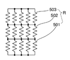
- FIG. 6 shows another modification of the discharge resistance portion R.
- each resistor of the first resistor group 501, each resistor of the second resistor group 502, and each resistor of the third resistor group 503 are connected in series. Five configurations are connected in parallel. That is, the discharge resistance portion R is composed of 3 series and 5 parallel connections of resistors.
- the withstand voltage of the discharge resistance unit R becomes high withstand voltage, and in the example of FIG. 4, the withstand voltage is two in series, so that the withstand voltage of one resistor is, for example, 600 V.
- the withstand voltage of the discharge resistance portion R can be 1200 V.
- the withstand voltage of the discharge resistance unit R can be 1200 V even if the withstand voltage of the resistor is lower than the above 600 V, for example, 400 V. That is, if the number of series is increased, a resistor having a low withstand voltage can be used.
- each connection node to which each resistor of the first resistor group 501 and each resistor of the second resistor group 502 is connected in series is short-circuited, and the second resistor is short-circuited.
- Each connection node to which each resistor of group 502 and each resistor of third resistor group 503 is connected in series is short-circuited, but may not be short-circuited.
- FIG. 7 is a perspective view showing an outline of the discharge circuit module 1X according to the modified example.
- a resistor (not shown) formed on the ceramic substrate 20 and a semiconductor chip (not shown) mounted on the ceramic substrate 20 are sealed with a sealing material 25 (resin or the like). It has a structure that is stopped and packaged.
- the upper surface of the ceramic substrate 20 is exposed to the outside, and a heat sink (not shown) can be joined to the exposed portion.
- the external terminal 30 protrudes from the side surface of the sealing material 25.
- the number of external terminals 30 is eight as shown in FIG. 7, for example, the four external terminals 30 other than the terminals corresponding to the external terminals T1 to T4 are NC terminals (electrically internally connected). Not a terminal).
- the discharge circuit module (1) is a discharge circuit module for discharging the capacitance portion (CX).
- the insulating substrate, the discharge resistance portion, and the semiconductor chip are packaged (first configuration).
- the insulating substrate may be a ceramic substrate (40) (second configuration).
- the DCB substrate (4) having the ceramic substrate (40) and the wiring portions (41, 42, 43) formed on the ceramic substrate is provided, and the resistor ( The 51, 52) and the semiconductor chip (6) may be configured to be electrically connected to the wiring portion (third configuration).
- the first external terminals (T1, T2) having the legs (T1B, T2B) are provided, and the wiring portions (43, 41) may be in contact with the legs. Good (fourth configuration).
- the second external terminal (T3, T4) is provided, and the wiring portion (41) is connected to the second external terminal by a bonding wire (W3, W1) or a bonding ribbon. It may be a configuration to be connected (fifth configuration).
- the wiring unit has a first wiring unit (41), a second wiring unit (42), and a third wiring unit (43).
- the first wiring unit, the second wiring unit, and the third wiring unit are arranged in this order in the first direction and extend in the second direction orthogonal to the first direction.
- the plurality of resistors constituting the first resistor group (51) are arranged in the second direction while connecting the first wiring portion and the second wiring portion.
- the plurality of resistors constituting the second resistor group (52) may be arranged in the second direction while connecting the second wiring portion and the third wiring portion (sixth). Configuration).
- a configuration having a copper plate (2) bonded to the ceramic substrate (40) may be used (seventh configuration).
- the ceramic substrate (40) and the copper plate (2) may be joined via the solder portion (3) (eighth configuration).
- any of the first to eighth configurations there is a configuration (7) for accommodating the insulating substrate (40), the discharge resistance portion (R), and the semiconductor chip (6). (9th configuration).
- the plate (2) which is joined to the insulating substrate (40) and is arranged below the case (7) is provided in the case and is provided in the vertical direction.
- the fixing hole portion (7A) through which the plate penetrates and the through hole portion (2A) provided in the plate and penetrating in the vertical direction may be configured to overlap each other in a top view (10th configuration).
- the discharge system (15) includes a discharge circuit module (1) having any of the above configurations, and a capacitance unit (CX) connected between the lines of the power supply line.
- CX capacitance unit
- the present disclosure can be used, for example, for discharging an X capacitor.
Landscapes
- Power Conversion In General (AREA)
- Chemical & Material Sciences (AREA)
- Engineering & Computer Science (AREA)
- Ceramic Engineering (AREA)
- Inverter Devices (AREA)
- Dc-Dc Converters (AREA)
Priority Applications (4)
| Application Number | Priority Date | Filing Date | Title |
|---|---|---|---|
| CN202180072606.4A CN116438646A (zh) | 2020-11-09 | 2021-10-26 | 放电电路模块 |
| DE112021004775.2T DE112021004775T5 (de) | 2020-11-09 | 2021-10-26 | Entladeschaltungsmodul |
| US18/034,957 US20230411367A1 (en) | 2020-11-09 | 2021-10-26 | Discharge circuit module |
| JP2022560731A JPWO2022097533A1 (enExample) | 2020-11-09 | 2021-10-26 |
Applications Claiming Priority (2)
| Application Number | Priority Date | Filing Date | Title |
|---|---|---|---|
| JP2020186408 | 2020-11-09 | ||
| JP2020-186408 | 2020-11-09 |
Publications (1)
| Publication Number | Publication Date |
|---|---|
| WO2022097533A1 true WO2022097533A1 (ja) | 2022-05-12 |
Family
ID=81457746
Family Applications (1)
| Application Number | Title | Priority Date | Filing Date |
|---|---|---|---|
| PCT/JP2021/039425 Ceased WO2022097533A1 (ja) | 2020-11-09 | 2021-10-26 | 放電回路モジュール |
Country Status (5)
| Country | Link |
|---|---|
| US (1) | US20230411367A1 (enExample) |
| JP (1) | JPWO2022097533A1 (enExample) |
| CN (1) | CN116438646A (enExample) |
| DE (1) | DE112021004775T5 (enExample) |
| WO (1) | WO2022097533A1 (enExample) |
Families Citing this family (1)
| Publication number | Priority date | Publication date | Assignee | Title |
|---|---|---|---|---|
| DE102024116415A1 (de) * | 2024-06-12 | 2025-12-18 | Schaeffler Technologies AG & Co. KG | Entladeeinrichtung zum aktiven oder passiven Entladen eines Leistungselektronikbauteils einer Leistungselektronik einer elektrischen Maschine und Leistungselektronikmodul |
Citations (5)
| Publication number | Priority date | Publication date | Assignee | Title |
|---|---|---|---|---|
| JPH09307366A (ja) * | 1996-05-16 | 1997-11-28 | Denso Corp | 半導体モジュール及び同半導体モジュールを用いたパワー回路 |
| JP2006013273A (ja) * | 2004-06-29 | 2006-01-12 | Fuji Electric Device Technology Co Ltd | 半導体装置 |
| JP2013179261A (ja) * | 2012-01-31 | 2013-09-09 | Aisin Aw Co Ltd | スイッチング素子ユニット |
| WO2016006065A1 (ja) * | 2014-07-09 | 2016-01-14 | 三菱電機株式会社 | 半導体装置 |
| WO2018186353A1 (ja) * | 2017-04-05 | 2018-10-11 | ローム株式会社 | パワーモジュール |
Family Cites Families (10)
| Publication number | Priority date | Publication date | Assignee | Title |
|---|---|---|---|---|
| US5523620A (en) * | 1994-02-14 | 1996-06-04 | Delco Electronics Corporation | Coplanar linear dual switch module |
| US5901044A (en) * | 1997-07-10 | 1999-05-04 | Ilc Data Device Corporation | Mini-module with upwardly directed leads |
| US6078501A (en) * | 1997-12-22 | 2000-06-20 | Omnirel Llc | Power semiconductor module |
| US6166464A (en) * | 1998-08-24 | 2000-12-26 | International Rectifier Corp. | Power module |
| DE10204200A1 (de) * | 2002-02-01 | 2003-08-21 | Conti Temic Microelectronic | Leistungsmodul |
| JP2005318690A (ja) * | 2004-04-27 | 2005-11-10 | Sanyo Electric Co Ltd | インバータモジュール |
| JP5511488B2 (ja) * | 2010-04-27 | 2014-06-04 | ダイキン工業株式会社 | 放電装置及び空調機 |
| WO2013002249A1 (ja) * | 2011-06-27 | 2013-01-03 | ローム株式会社 | 半導体モジュール |
| JP2013158211A (ja) | 2012-01-31 | 2013-08-15 | Canon Inc | 放電回路及び放電回路を備えた電源 |
| JP6361466B2 (ja) * | 2014-10-28 | 2018-07-25 | 株式会社デンソー | 放電制御装置、及び、これを備える電力変換装置 |
-
2021
- 2021-10-26 JP JP2022560731A patent/JPWO2022097533A1/ja active Pending
- 2021-10-26 US US18/034,957 patent/US20230411367A1/en not_active Abandoned
- 2021-10-26 DE DE112021004775.2T patent/DE112021004775T5/de active Pending
- 2021-10-26 CN CN202180072606.4A patent/CN116438646A/zh active Pending
- 2021-10-26 WO PCT/JP2021/039425 patent/WO2022097533A1/ja not_active Ceased
Patent Citations (5)
| Publication number | Priority date | Publication date | Assignee | Title |
|---|---|---|---|---|
| JPH09307366A (ja) * | 1996-05-16 | 1997-11-28 | Denso Corp | 半導体モジュール及び同半導体モジュールを用いたパワー回路 |
| JP2006013273A (ja) * | 2004-06-29 | 2006-01-12 | Fuji Electric Device Technology Co Ltd | 半導体装置 |
| JP2013179261A (ja) * | 2012-01-31 | 2013-09-09 | Aisin Aw Co Ltd | スイッチング素子ユニット |
| WO2016006065A1 (ja) * | 2014-07-09 | 2016-01-14 | 三菱電機株式会社 | 半導体装置 |
| WO2018186353A1 (ja) * | 2017-04-05 | 2018-10-11 | ローム株式会社 | パワーモジュール |
Also Published As
| Publication number | Publication date |
|---|---|
| CN116438646A (zh) | 2023-07-14 |
| US20230411367A1 (en) | 2023-12-21 |
| JPWO2022097533A1 (enExample) | 2022-05-12 |
| DE112021004775T5 (de) | 2023-08-31 |
Similar Documents
| Publication | Publication Date | Title |
|---|---|---|
| US6441520B1 (en) | Power module | |
| US7122890B2 (en) | Low cost power semiconductor module without substrate | |
| US7149088B2 (en) | Half-bridge power module with insert molded heatsinks | |
| JP5169353B2 (ja) | パワーモジュール | |
| US7301235B2 (en) | Semiconductor device module with flip chip devices on a common lead frame | |
| US9673129B2 (en) | Semiconductor device | |
| US8526189B2 (en) | Power module | |
| CN114175234A (zh) | 半导体装置及电子装置 | |
| JPH0855956A (ja) | 駆動回路装置モジュール | |
| CN110176446B (zh) | 半导体装置 | |
| US7215023B2 (en) | Power module | |
| WO2001082376A1 (fr) | Dispositif a semi-conducteur | |
| CN113692697B (zh) | 电子电路单元 | |
| US6822399B2 (en) | Half-bridge circuit | |
| JP2008187145A (ja) | 回路装置 | |
| US6664629B2 (en) | Semiconductor device | |
| US20240244750A1 (en) | Semiconductor module | |
| CN116438646A (zh) | 放电电路模块 | |
| JP2010251582A (ja) | Dc−dcコンバータ | |
| JP6060053B2 (ja) | パワー半導体装置 | |
| CN117425957A (zh) | 半导体装置 | |
| US20220399259A1 (en) | Power Semiconductor Module | |
| CN214313198U (zh) | 一种功率组件 | |
| JP2000082775A (ja) | 半導体モジュ―ル | |
| CN111554667B (zh) | 功率半导体装置 |
Legal Events
| Date | Code | Title | Description |
|---|---|---|---|
| 121 | Ep: the epo has been informed by wipo that ep was designated in this application |
Ref document number: 21889086 Country of ref document: EP Kind code of ref document: A1 |
|
| ENP | Entry into the national phase |
Ref document number: 2022560731 Country of ref document: JP Kind code of ref document: A |
|
| 122 | Ep: pct application non-entry in european phase |
Ref document number: 21889086 Country of ref document: EP Kind code of ref document: A1 |