WO2022097307A1 - 電力変換装置の制御装置および電力変換装置用抵抗器 - Google Patents
電力変換装置の制御装置および電力変換装置用抵抗器 Download PDFInfo
- Publication number
- WO2022097307A1 WO2022097307A1 PCT/JP2020/041771 JP2020041771W WO2022097307A1 WO 2022097307 A1 WO2022097307 A1 WO 2022097307A1 JP 2020041771 W JP2020041771 W JP 2020041771W WO 2022097307 A1 WO2022097307 A1 WO 2022097307A1
- Authority
- WO
- WIPO (PCT)
- Prior art keywords
- voltage
- power converter
- power
- controlled
- recognition unit
- Prior art date
- Legal status (The legal status is an assumption and is not a legal conclusion. Google has not performed a legal analysis and makes no representation as to the accuracy of the status listed.)
- Ceased
Links
Images



Classifications
-
- H—ELECTRICITY
- H02—GENERATION; CONVERSION OR DISTRIBUTION OF ELECTRIC POWER
- H02M—APPARATUS FOR CONVERSION BETWEEN AC AND AC, BETWEEN AC AND DC, OR BETWEEN DC AND DC, AND FOR USE WITH MAINS OR SIMILAR POWER SUPPLY SYSTEMS; CONVERSION OF DC OR AC INPUT POWER INTO SURGE OUTPUT POWER; CONTROL OR REGULATION THEREOF
- H02M7/00—Conversion of AC power input into DC power output; Conversion of DC power input into AC power output
- H02M7/42—Conversion of DC power input into AC power output without possibility of reversal
- H02M7/44—Conversion of DC power input into AC power output without possibility of reversal by static converters
- H02M7/48—Conversion of DC power input into AC power output without possibility of reversal by static converters using discharge tubes with control electrode or semiconductor devices with control electrode
- H02M7/493—Conversion of DC power input into AC power output without possibility of reversal by static converters using discharge tubes with control electrode or semiconductor devices with control electrode the static converters being arranged for operation in parallel
-
- H—ELECTRICITY
- H02—GENERATION; CONVERSION OR DISTRIBUTION OF ELECTRIC POWER
- H02J—ELECTRIC POWER NETWORKS; CIRCUIT ARRANGEMENTS OR SYSTEMS FOR SUPPLYING OR DISTRIBUTING ELECTRIC POWER; SYSTEMS FOR STORING ELECTRIC ENERGY
- H02J7/00—Circuit arrangements for charging or discharging batteries or for supplying loads from batteries
-
- H—ELECTRICITY
- H02—GENERATION; CONVERSION OR DISTRIBUTION OF ELECTRIC POWER
- H02M—APPARATUS FOR CONVERSION BETWEEN AC AND AC, BETWEEN AC AND DC, OR BETWEEN DC AND DC, AND FOR USE WITH MAINS OR SIMILAR POWER SUPPLY SYSTEMS; CONVERSION OF DC OR AC INPUT POWER INTO SURGE OUTPUT POWER; CONTROL OR REGULATION THEREOF
- H02M1/00—Details of apparatus for conversion
- H02M1/0003—Details of control, feedback or regulation circuits
- H02M1/0006—Arrangements for supplying an adequate voltage to the control circuit of converters
-
- H—ELECTRICITY
- H02—GENERATION; CONVERSION OR DISTRIBUTION OF ELECTRIC POWER
- H02M—APPARATUS FOR CONVERSION BETWEEN AC AND AC, BETWEEN AC AND DC, OR BETWEEN DC AND DC, AND FOR USE WITH MAINS OR SIMILAR POWER SUPPLY SYSTEMS; CONVERSION OF DC OR AC INPUT POWER INTO SURGE OUTPUT POWER; CONTROL OR REGULATION THEREOF
- H02M1/00—Details of apparatus for conversion
- H02M1/08—Circuits specially adapted for the generation of control voltages for semiconductor devices incorporated in static converters
- H02M1/083—Circuits specially adapted for the generation of control voltages for semiconductor devices incorporated in static converters for the ignition at the zero crossing of the voltage or the current
-
- H—ELECTRICITY
- H02—GENERATION; CONVERSION OR DISTRIBUTION OF ELECTRIC POWER
- H02M—APPARATUS FOR CONVERSION BETWEEN AC AND AC, BETWEEN AC AND DC, OR BETWEEN DC AND DC, AND FOR USE WITH MAINS OR SIMILAR POWER SUPPLY SYSTEMS; CONVERSION OF DC OR AC INPUT POWER INTO SURGE OUTPUT POWER; CONTROL OR REGULATION THEREOF
- H02M1/00—Details of apparatus for conversion
- H02M1/12—Arrangements for reducing harmonics from AC input or output
- H02M1/123—Suppression of common mode voltage or current
-
- H—ELECTRICITY
- H02—GENERATION; CONVERSION OR DISTRIBUTION OF ELECTRIC POWER
- H02M—APPARATUS FOR CONVERSION BETWEEN AC AND AC, BETWEEN AC AND DC, OR BETWEEN DC AND DC, AND FOR USE WITH MAINS OR SIMILAR POWER SUPPLY SYSTEMS; CONVERSION OF DC OR AC INPUT POWER INTO SURGE OUTPUT POWER; CONTROL OR REGULATION THEREOF
- H02M1/00—Details of apparatus for conversion
- H02M1/32—Means for protecting converters other than automatic disconnection
Definitions
- the present disclosure relates to a control device for a power conversion device and a resistor for the power conversion device.
- Patent Document 1 discloses a power conversion system. In the power system, the difference in DC voltage between a plurality of power converters is suppressed. Therefore, cross current between a plurality of power converters can be suppressed.
- An object of the present disclosure is to provide a control device for a power conversion device and a resistor for a power conversion device that can suppress cross current between a plurality of power converters with a simple configuration.
- the DC side of the plurality of power converters is not connected in parallel, but the AC side of the plurality of power converters is connected in parallel, and the positive currents on the DC side of the plurality of power converters are connected to each other.
- the negative electrodes are connected to a common potential point via a plurality of resistors, a voltage that recognizes the voltage applied to the resistor connected to the power converter to be controlled among the plurality of resistors. Control to control the DC voltage of the power converter to be controlled so that the magnitude of the voltage recognized by the voltage recognition unit is smaller based on the voltage recognized by the recognition unit and the voltage recognition unit.
- the DC side of the plurality of power converters is not connected in parallel, but the AC side of the plurality of power converters is connected in parallel, and the positive currents on the DC side of the plurality of power converters are connected to each other.
- the negative electrodes are connected to a common potential point via a plurality of resistors, a voltage that recognizes the voltage applied to the resistor connected to the power converter to be controlled among the plurality of resistors.
- the output zero-phase voltage of the power converter to be controlled is controlled so that the magnitude of the voltage recognized by the voltage recognition unit is smaller based on the voltage recognized by the recognition unit and the voltage recognition unit. It is equipped with a control unit.
- the resistor for a power converter according to the present disclosure corresponds to a state in which one end to be grounded and the AC side of the plurality of power converters are connected in parallel without connecting the DC sides of the plurality of power converters in parallel. The other end connected to the DC side of the converter was provided.
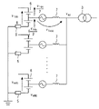
- FIG. 1 It is a block diagram of the power conversion system to which the control device of the power conversion device in Embodiment 1 is applied. It is a figure which shows the equivalent circuit paying attention to the AC zero-phase component of the power conversion system to which the control device of the power conversion device in Embodiment 1 is applied. It is a figure which shows the control block of the control device of the power conversion device in Embodiment 1. FIG. It is a hardware block diagram of the control device of the power conversion device in Embodiment 1. FIG.
- FIG. 1 is a configuration diagram of a power conversion system to which the control device of the power conversion device according to the first embodiment is applied.
- each of the plurality of DC power supplies 1 is provided so as to be able to output DC power.
- each of the plurality of DC power sources 1 is a photovoltaic power generation device.
- System 2 is operated by an electric power company or the like. The system 2 is provided so as to be able to output AC power.
- the interconnection transformer 3 is connected between the DC power supply 1 and the system 2.
- the plurality of power conversion devices 4 are provided corresponding to the plurality of DC power supplies 1. Each of the plurality of power conversion devices 4 is connected between the corresponding DC power supply 1 and the interconnection transformer device 3. The DC sides of the plurality of power converters 4 are not connected in parallel. The AC side of the plurality of power conversion devices 4 is connected in parallel.
- the plurality of resistors 5 are provided corresponding to the plurality of power conversion devices 4, respectively. One end of each of the plurality of resistors 5 is grounded. The other end of each of the plurality of resistors 5 is connected to the negative electrode on the DC side of the corresponding power conversion device 4.
- each of the plurality of power converters 4 includes a power converter 6, a reactor 7, and a control device 8.
- the power converter 6 is provided so as to be able to convert the DC power from the DC power source 1 into AC power.
- the reactor 7 is provided so as to be able to absorb the harmonics of the AC power from the power converter 6.
- the control device 8 includes a voltage recognition unit 8a and a control unit 8b.
- the voltage recognition unit 8a recognizes the voltage to ground on the DC side of the power converter 6 to be controlled. For example, the voltage recognition unit 8a recognizes the voltage between the DC negative electrode and the ground of the power converter 6 to be controlled based on the detection value of the voltage detection unit (not shown).
- the control unit 8b controls the power converter 6 to be controlled based on the DC voltage recognized by the voltage recognition unit 8a.
- Control the DC voltage For example, the control unit 8b of the power converter 6 to be controlled so that the voltage to ground on the DC side of the power converter 6 to be controlled becomes smaller based on the voltage to ground on the DC side recognized by the voltage recognition unit 8a. Controls the output zero-phase voltage.
- FIG. 2 is a diagram showing an equivalent circuit focusing on the AC zero-phase component of the power conversion system to which the control device of the power conversion device according to the first embodiment is applied.
- the voltage to ground viNG of the negative electrode on the DC side of the i-th power converter 6 is expressed by the following equation (1).
- the vidc is the DC voltage of the i-th power converter 6.
- v isoc is the output zero-phase voltage of the parallel connection point with respect to the virtual neutral point on the DC side of the i-th power converter 6.
- Equation (2) represents the average value of the output zero-phase voltage of the parallel connection point with respect to the DC side virtual neutral point potential other than the i-th power converter 6.
- Equation (3) represents an average value of DC voltage other than the i-th power converter 6.
- the zero-phase voltage vsoc is smaller than the DC voltage.
- the difference in the zero-phase voltage vsoc among the plurality of power converters 6 is small. Therefore, the second term on the right side is dominant in the equation (1) for any i-th power converter 6.
- the following equation (5) is the average value of the DC voltage other than the i-power converter 6.
- the control device 8 recognizes the voltage to ground viNG using the voltage recognition unit 8a. For example, the control device 8 controls the DC voltage vidc of the i-th power converter 6 so that the ground voltage v iNG of the i-th power converter 6 becomes smaller. For example, the control device 8 controls the output zero-phase voltage v isoc of the i-th power converter 6 so that the ground voltage v iNG of the i-th power converter 6 becomes smaller.
- FIG. 3 is a diagram showing a control block of the control device of the power conversion device according to the first embodiment.
- the control device 8 includes a first control block 9, a second control block 10, a third control block 11, a fourth control block 12, and a fifth control block 13.
- the first control block 9 receives input of information on the value of the DC voltage vidc of the i-th power converter 6.
- the first control block 9 receives input of information on the value of the DC current iidc of the i-th power converter 6.
- the first control block 9 outputs information on the first provisional voltage command value v dc_MPPT * when MPPT control is performed based on the value of the DC voltage V idc and the value of the DC current i idc .
- the second control block 10 receives input of information on the value of the voltage to ground v iNG of the i-th power converter 6.
- the second control block 10 outputs a first output value and a second output value f_deadband corresponding to the value of the voltage to ground V iNG .
- the second output value f_deadband becomes 0.
- the first output value is 0.
- the second output value f_deadband becomes 1.
- the first output value has an absolute value equal to the difference between the absolute value of the voltage to ground v iNG of the i-th power converter 6 and the preset threshold value (dead band) v NGdb , and the sign is the i-power conversion.
- the value is equal to that of the ground voltage viNG of the vessel 6.
- the third control block 11 attaches the input of the information of the first provisional voltage command value vdc_MPPT * from the first control block 9.
- the third control block 11 receives input of information from the second control block 10 with the second output value f_deadband.
- the third control block 11 outputs the value of the first provisional voltage command value v dc_MPPT * as it is.
- the third control block 11 stores the value of the first provisional voltage command value v dc_MPPT * when the second output value f_deadband from the second control block 10 changes from 0 to 1, and from the second control block 10. Until the second output value f_deadband becomes 0 next time, the stored first provisional voltage command value v dc_MPPT * is output.
- the fourth control block 12 accepts the input of the information of the first output value from the second control block 10.
- the fourth control block 12 outputs a value controlled by PI so that the first output value from the second control block 10 approaches 0.
- the fifth control block 13 receives input of information of the first provisional voltage command value vdc_MPPT * from the first control block 9.
- the fifth control block 13 receives the input of the information of the second provisional voltage command value v dc_NG * , which is the sum of the output value from the third control block 11 and the output value from the fourth control block 12.
- the fifth control block 13 receives input of information of the second output value f_deadband from the second control block 10.
- the fifth control block 13 uses the first provisional voltage command value v dc_MPPT * as the voltage command value v dc * and direct current of the i-power converter 6. Control the voltage.
- the fifth control block 13 uses the second provisional voltage command value v dc_NG * as the voltage command value v dc * and direct current of the i-power converter 6. Control the voltage.
- the voltage to ground v iNG of the i-th power converter 6 is controlled to be equal to or lower than the preset threshold value v NGdb .
- the difference between the i-th power converter 6 and the power converter 6 other than the i-th power converter 6 becomes small.
- the value represented by the following equation (6) becomes smaller.
- the voltage to ground on the DC side of the power converter 6 to be controlled becomes smaller based on the voltage to ground on the DC side of the power converter 6 to be controlled.
- the DC voltage of the power converter 6 to be controlled is controlled in this way. Therefore, the difference in DC voltage between the plurality of power converters 6 can be reduced. As a result, it is possible to suppress the cross current transmitted through the stray capacitance on the DC side among the plurality of power converters 6.
- the DC power source 1 is a photovoltaic power generation device
- the negative electrode is grounded via a resistor and the negative ground voltage applied to the negative electrode of the solar cell is suppressed, so that the solar cell deteriorates due to the PID phenomenon. Can be suppressed.
- the control device 8 is controlled so that the voltage to ground on the DC side of the power converter 6 to be controlled becomes smaller based on the voltage to ground on the DC side of the power converter 6 to be directly controlled by itself. It controls the DC voltage of the power converter 6 of the above, but it is not necessary to recognize the value of the ground voltage or the DC voltage of another power converter 6 on the DC side which is not directly controlled by itself. Therefore, communication between a plurality of power converters 4 and measurement of DC voltage of different power converters 6 are unnecessary. Therefore, with a simple configuration, it is possible to suppress cross currents among the plurality of power converters 6.
- control device 8 controls the DC voltage of the power converter 6 to be controlled so that the amount exceeding a preset threshold value in the voltage to ground on the DC side of the power converter 6 to be controlled becomes smaller. Therefore, in each of the plurality of power conversion devices 4, MPPT control can be performed within a range in which the magnitude of the voltage to ground does not matter.
- control device 8 has an output zero phase of the power converter 6 to be controlled so that the voltage to ground on the DC side of the power converter 6 to be controlled becomes smaller based on the DC voltage of the power converter 6 to be controlled. Control the voltage. Therefore, the difference in DC voltage between the plurality of power converters 6 can be reduced. As a result, cross current between the plurality of power converters 6 can be suppressed. At this time, DC voltage control can be freely performed for MPPT control in each of the plurality of power conversion devices 4.
- control device 8 controls the output zero-phase voltage of the power converter 6 to be controlled so that the amount exceeding a preset threshold value in the voltage to ground on the DC side of the power converter 6 to be controlled becomes smaller. do. In this case as well, cross flow between the plurality of power converters 6 can be suppressed. At this time, DC voltage control can be freely performed for MPPT control in each of the plurality of power conversion devices 4.
- the resistor 5 can be miniaturized.
- the resistance value of the resistor 5 may be increased. Also in this case, with a simple configuration, it is possible to suppress cross current through the ground wire between the plurality of power converters 6.
- the control device 8 is applied to the resistor by the voltage recognition unit 8a instead of the voltage to ground on the DC side of the power converter 6 to be controlled. Recognizing the voltage, the control device 8 recognizes the DC voltage or the output zero of the power converter 6 to be controlled so that the magnitude of the voltage recognized by the voltage recognition unit 8a becomes smaller based on the voltage recognized by the voltage recognition unit 8a.
- the phase voltage may be controlled.
- the voltage recognized by the voltage recognition unit 8a becomes equal to the right side of the equation (1), and similarly, the difference in DC voltage between the plurality of power converters 6 can be reduced. As a result, cross current between the plurality of power converters 6 can be suppressed.
- the equation (1) is derived as follows.
- the output zero-phase potential vio of the i-th power converter 6 is defined by the following equation (7).
- the zero-phase current iio of the i-th power converter 6 is defined by the following equation (8).
- the DC side virtual neutral point potential vidc is defined by the following equation (10).
- viP is the DC positive electrode potential of the i-th power converter 6.
- v iN is the DC negative electrode potential of the i-th power converter 6.
- vidc is the DC voltage of the i-th power converter 6.
- viNG is the voltage to ground of the DC negative electrode of the i-th power converter 6.
- v soG is the zero-phase voltage to ground at the AC-side parallel connection point of the i-th power converter 6.
- R is the resistance value of the resistor 5.
- i iG is a current flowing through the resistor 5.
- Equation (1) is derived from equations (14) and (22).
- FIG. 4 is a hardware configuration diagram of the control device of the power conversion device according to the first embodiment.
- Each function of the control device 8 can be realized by a processing circuit.
- the processing circuit comprises at least one processor 100a and at least one memory 100b.
- the processing circuit comprises at least one dedicated hardware 200.
- each function of the control device 8 is realized by software, firmware, or a combination of software and firmware. At least one of the software and firmware is written as a program. At least one of the software and firmware is stored in at least one memory 100b. At least one processor 100a realizes each function of the control device 8 by reading and executing a program stored in at least one memory 100b. At least one processor 100a is also referred to as a central processing unit, a processing unit, an arithmetic unit, a microprocessor, a microcomputer, and a DSP.
- At least one memory 100b is a non-volatile or volatile semiconductor memory such as RAM, ROM, flash memory, EPROM, EEPROM, a magnetic disk, a flexible disk, an optical disk, a compact disk, a mini disk, a DVD, or the like.
- the processing circuit comprises at least one dedicated hardware 200
- the processing circuit may be implemented, for example, as a single circuit, a composite circuit, a programmed processor, a parallel programmed processor, an ASIC, an FPGA, or a combination thereof.
- each function of the control device 8 is realized by a processing circuit.
- each function of the control device 8 is collectively realized by a processing circuit.
- a part may be realized by the dedicated hardware 200, and the other part may be realized by software or firmware.
- the function of the control unit 8b is realized by a processing circuit as dedicated hardware 200, and for the functions other than the function of the control unit 8b, at least one processor 100a reads a program stored in at least one memory 100b. It may be realized by executing the above.
- the processing circuit realizes each function of the control device 8 by hardware 200, software, firmware, or a combination thereof.
- the power conversion device of the present disclosure can be used for the power conversion system.
Landscapes
- Engineering & Computer Science (AREA)
- Power Engineering (AREA)
- Inverter Devices (AREA)
- Rectifiers (AREA)
- Supply And Distribution Of Alternating Current (AREA)
- Charge And Discharge Circuits For Batteries Or The Like (AREA)
Abstract
簡素な構成で、複数の電力変換器の間における横流を抑制することができる電力変換装置の制御装置および電力変換装置用抵抗器を提供することである。電力変換装置の制御装置は、複数の電力変換器の直流側が並列接続されずに前記複数の電力変換器の交流側が並列接続された状態において、制御対象の電力変換器の直流側の対地電圧を認識する電圧認識部と、前記電圧認識部により認識された直流側の対地電圧に基づいて前記制御対象の電力変換器の直流側の対地電圧がより小さくなるように前記制御対象の電力変換器の直流電圧を制御する制御部と、を備えた。
Description
本開示は、電力変換装置の制御装置および電力変換装置用抵抗器に関する。
特許文献1は、電力変換システムを開示する。当該電力システムにおいては、複数の電力変換器における直流電圧の差が抑制される。このため、複数の電力変換器の間における横流が抑制され得る。
しかしながら、特許文献1に記載の電力変換システムにおいては、複数の電力変換器にそれぞれ対応した複数の制御装置の間において互いの直流電圧の情報をやり取りしたり、共通の制御装置で複数の電力変換器の直流電圧を認識して複数の電力変換器に対して直流電圧指令値を出力したりする必要がある。このため、電力変換システムが複雑になる。
本開示は、上述の課題を解決するためになされた。本開示の目的は、簡素な構成で、複数の電力変換器の間における横流を抑制することができる電力変換装置の制御装置および電力変換装置用抵抗器を提供することである。
本開示に係る電力変換装置の制御装置は、複数の電力変換器の直流側が並列接続されずに前記複数の電力変換器の交流側が並列接続され、前記複数の電力変換器の直流側の正極同士または負極同士が複数の抵抗器を介して共通の電位点に接続された状態において、前記複数の抵抗器のうち制御対象の電力変換器に接続された抵抗器に印可される電圧を認識する電圧認識部と、前記電圧認識部により認識された前記電圧に基づいて前記電圧認識部により認識された前記電圧の大きさがより小さくなるように前記制御対象の電力変換器の直流電圧を制御する制御部と、を備えた。
本開示に係る電力変換装置の制御装置は、複数の電力変換器の直流側が並列接続されずに前記複数の電力変換器の交流側が並列接続され、前記複数の電力変換器の直流側の正極同士または負極同士が複数の抵抗器を介して共通の電位点に接続された状態において、前記複数の抵抗器のうち制御対象の電力変換器に接続された抵抗器に印可される電圧を認識する電圧認識部と、前記電圧認識部により認識された前記電圧に基づいて前記電圧認識部により認識された前記電圧の大きさがより小さくなるように前記制御対象の電力変換器の出力零相電圧を制御する制御部と、を備えた。
本開示に係る電力変換装置用抵抗器は、接地される一端と、複数の電力変換器の直流側が並列接続されずに前記複数の電力変換器の交流側が並列接続された状態において、対応した電力変換器の直流側に接続される他端と、を備えた。
本開示によれば、簡素な構成で、複数の電力変換器の間における横流を抑制することができる。
実施の形態について添付の図面に従って説明する。なお、各図中、同一または相当する部分には同一の符号が付される。当該部分の重複説明は適宜に簡略化ないし省略する。
実施の形態1.
図1は実施の形態1における電力変換装置の制御装置が適用される電力変換システムの構成図である。
図1は実施の形態1における電力変換装置の制御装置が適用される電力変換システムの構成図である。
図1において、複数の直流電源1の各々は、直流電力を出力し得るように設けられる。例えば、複数の直流電源1の各々は、太陽光発電装置である。系統2は、電力会社等に運用される。系統2は、交流電力を出力し得るように設けられる。連系変圧装置3は、直流電源1と系統2との間に接続される。
複数の電力変換装置4は、複数の直流電源1にそれぞれ対応して設けられる。複数の電力変換装置4の各々は、対応した直流電源1と連系変圧装置3との間に接続される。複数の電力変換装置4の直流側は、並列接続されない。複数の電力変換装置4の交流側は、並列接続される。
複数の抵抗器5は、複数の電力変換装置4にそれぞれ対応して設けられる。複数の抵抗器5の各々の一端は、接地される。複数の抵抗器5の各々の他端は、対応した電力変換装置4の直流側において負極に接続される。
例えば、複数の電力変換装置4の各々は、電力変換器6とリアクトル7と制御装置8とを備える。
電力変換器6は、直流電源1からの直流電力を交流電力に変換し得るように設けられる。例えば、リアクトル7は、電力変換器6からの交流電力の高調波を吸収し得るように設けられる。制御装置8は、電圧認識部8aと制御部8bとを備える。
電圧認識部8aは、制御対象の電力変換器6の直流側の対地電圧を認識する。例えば、電圧認識部8aは、図示されない電圧検出部の検出値に基づいて制御対象の電力変換器6の直流負極と接地の間の電圧を認識する。制御部8bは、電圧認識部8aにより認識された直流電圧に基づいて制御対象の電力変換器6を制御する。
例えば、制御部8bは、電圧認識部8aにより認識された直流側の対地電圧に基づいて制御対象の電力変換器6の直流側の対地電圧がより小さくなるように制御対象の電力変換器6の直流電圧を制御する。例えば、制御部8bは、電圧認識部8aにより認識された直流側の対地電圧に基づいて制御対象の電力変換器6の直流側の対地電圧がより小さくなるように制御対象の電力変換器6の出力零相電圧を制御する。
次に、図2を用いて、制御装置8による電力変換器6の制御の概要を説明する。
図2は実施の形態1における電力変換装置の制御装置が適用される電力変換システムの交流零相成分に着目した等価回路を示す図である。
図2は実施の形態1における電力変換装置の制御装置が適用される電力変換システムの交流零相成分に着目した等価回路を示す図である。
第i電力変換器6の直流側の負極の対地電圧viNGは、次の(1)式で表される。

(1)式において、vidcは、第i電力変換器6の直流電圧である。visocは、第i電力変換器6の直流側の仮想中性点に対する並列接続点の出力零相電圧である。
また、次の(2)式と(3)式とが成立する。


(2)式は、第i電力変換器6以外の直流側仮想中性点電位に対する並列接続点の出力零相電圧の平均値を表す。(3)式は、第i電力変換器6以外の直流電圧の平均値を表す。
通常、零相電圧visocは、直流電圧よりも小さい。複数の電力変換器6の間において、零相電圧visocの差は小さい。このため、任意の第i電力変換器6に対し、(1)式において、右辺第2項が支配的となる。
(1)式の右辺第2項において、次の(4)式は定数である。

(1)式の右辺第2項において、次の(5)式は第i電力変換器6以外の直流電圧の平均値である。

制御装置8は、電圧認識部8aを用いて対地電圧viNGを認識する。例えば、制御装置8は、第i電力変換器6の対地電圧viNGがより小さくなるように第i電力変換器6の直流電圧vidcを制御する。例えば、制御装置8は、第i電力変換器6の対地電圧viNGがより小さくなるように第i電力変換器6の出力零相電圧visocを制御する。
次に、図3を用いて、制御装置8による電力変換器6の制御の詳細を説明する。
図3は実施の形態1における電力変換装置の制御装置の制御ブロックを示す図である。
図3は実施の形態1における電力変換装置の制御装置の制御ブロックを示す図である。
図3に示されるように、制御装置8は、第1制御ブロック9と第2制御ブロック10と第3制御ブロック11と第4制御ブロック12と第5制御ブロック13とを備える。
第1制御ブロック9は、第i電力変換器6の直流電圧vidcの値の情報の入力を受け付ける。第1制御ブロック9は、第i電力変換器6の直流電流iidcの値の情報の入力を受け付ける。第1制御ブロック9は、直流電圧Vidcの値と直流電流iidcの値とに基づいたMPPT制御を行う際の第1暫定電圧指令値vdc_MPPT
*の情報を出力する。
第2制御ブロック10は、第i電力変換器6の対地電圧viNGの値の情報の入力を受け付ける。第2制御ブロック10は、対地電圧ViNGの値に応じた第1出力値と第2出力値f_deadbandとを出力する。第i電力変換器6の対地電圧ViNGの絶対値が予め設定された閾値vNGdb以下の場合、第2出力値f_deadbandは0となる。また、第1出力値は0となる。第i電力変換器6の対地電圧viNGの絶対値が予め設定された閾値(デッドバンド)vNGdbよりも大きい場合、第2出力値f_deadbandは1となる。また、第1出力値は、第i電力変換器6の対地電圧viNGの絶対値と、予め設定された閾値(デッドバンド)vNGdbとの差に絶対値が等しく、符号が第i電力変換器6の対地電圧viNGのそれに等しい値となる。
第3制御ブロック11は、第1制御ブロック9からの第1暫定電圧指令値vdc_MPPT
*の情報の入力を付けつける。第3制御ブロック11は、第2制御ブロック10からの第2出力値f_deadbandとの情報の入力を受け付ける。第3制御ブロック11は、第2出力値f_deadbandが0のとき、第1暫定電圧指令値vdc_MPPT
*の値をそのまま出力する。第3制御ブロック11は、第2制御ブロック10からの第2出力値f_deadbandが0から1に変化したときの第1暫定電圧指令値vdc_MPPT
*の値を記憶し、第2制御ブロック10からの第2出力値f_deadbandが次に0になるまでの間、記憶した第1暫定電圧指令値vdc_MPPT
*の値を出力する。
第4制御ブロック12は、第2制御ブロック10からの第1出力値の情報の入力を受け付ける。第4制御ブロック12は、第2制御ブロック10からの第1出力値が0に近づくようにPI制御した値を出力する。
第5制御ブロック13は、第1制御ブロック9からの第1暫定電圧指令値vdc_MPPT
*の情報の入力を受け付ける。第5制御ブロック13は、第3制御ブロック11からの出力値と第4制御ブロック12からの出力値とを合算した第2暫定電圧指令値vdc_NG
*の情報の入力を受け付ける。第5制御ブロック13は、第2制御ブロック10からの第2出力値f_deadbandの情報の入力を受け付ける。第2制御ブロック10からの第2出力値f_deadbandが0である場合、第5制御ブロック13は、第1暫定電圧指令値vdc_MPPT
*を電圧指令値vdc
*として第i電力変換器6の直流電圧を制御する。第2制御ブロック10からの第2出力値f_deadbandが1である場合、第5制御ブロック13は、第2暫定電圧指令値vdc_NG
*を電圧指令値vdc
*として第i電力変換器6の直流電圧を制御する。
この場合、第i電力変換器6の対地電圧viNGは、予め設定された閾値vNGdb以下に制御される。その結果、第i電力変換器6と第i電力変換器6以外の電力変換器6との差が小さくなる。具体的には、以下の(6)式で表される値が小さくなる。

以上で説明した実施の形態1によれば、制御装置8は、制御対象の電力変換器6の直流側の対地電圧に基づいて制御対象の電力変換器6の直流側の対地電圧がより小さくなるように制御対象の電力変換器6の直流電圧を制御する。このため、複数の電力変換器6の間の直流電圧の差を小さくすることができる。その結果、複数の電力変換器6の間において直流側の浮遊容量を伝う横流を抑制することができる。また、直流電源1が太陽光発電装置である場合、負極が抵抗器を介して接地され、太陽電池の負極に印可される負の対地電圧が抑制されることで、PID現象により太陽電池が劣化することを抑制できる。
この際、制御装置8は、自身が直接の制御対象とする電力変換器6の直流側の対地電圧に基づいて制御対象の電力変換器6の直流側の対地電圧がより小さくなるように制御対象の電力変換器6の直流電圧を制御するが、自身が直接の制御対象としない他の電力変換器6の直流側の対地電圧や直流電圧の値を認識する必要はない。したがって、複数の電力変換装置4の間での通信、異なる電力変換器6の直流電圧の測定等は不要である。このため、簡素な構成で、複数の電力変換器6の間における横流を抑制することができる。
例えば、制御装置8は、制御対象の電力変換器6の直流側の対地電圧において予め設定された閾値を超えた分がより小さくなるように制御対象の電力変換器6の直流電圧を制御する。このため、複数の電力変換装置4の各々において、対地電圧の大きさが問題にならない範囲でMPPT制御を行うことができる。
また、制御装置8は、制御対象の電力変換器6の直流電圧に基づいて制御対象の電力変換器6の直流側の対地電圧がより小さくなるように制御対象の電力変換器6の出力零相電圧を制御する。このため、複数の電力変換器6の間の直流電圧の差を小さくすることができる。その結果、複数の電力変換器6の間における横流を抑制することができる。この際、複数の電力変換装置4の各々において、MPPT制御のために直流電圧制御を自由に行うことができる。
例えば、制御装置8は、制御対象の電力変換器6の直流側の対地電圧において予め設定された閾値を超えた分がより小さくなるように制御対象の電力変換器6の出力零相電圧を制御する。この場合も、複数の電力変換器6の間における横流を抑制することができる。この際、複数の電力変換装置4の各々において、MPPT制御のために直流電圧制御を自由に行うことができる。
また、直流側の対地電圧がより小さくなることで、抵抗器5の最大電圧が下がる。抵抗器5の最大電圧が下がることで、抵抗器5の消費電力が抑制される。このため、抵抗器5を小型化することができる。
また、直流側の対地電圧がより小さくなるように電力変換器6が制御されない場合は、抵抗器5の抵抗値を大きくすればよい。この場合も、簡素な構成で、複数の電力変換器6の間において接地線を介した横流を抑制することができる。
また、各々の一端が複数の電力変換器6の負極に接続される複数の抵抗器5において、電力変換器6の負極に接続されない他方の一端を接地せずに、代わりに複数の電力変換装置4のすべてに対して共通の任意の電位点に接続し、制御装置8は電圧認識部8aによって、制御対象の電力変換器6の直流側の対地電圧の代わりに前記の抵抗器に印可される電圧を認識し、制御装置8は電圧認識部8aが認識した電圧に基づいて電圧認識部8aが認識した電圧の大きさがより小さくなるように制御対象の電力変換器6の直流電圧または出力零相電圧を制御するようにしても良い。この場合でも、電圧認識部8aが認識する電圧は、(1)式の右辺に等しくなり、同様に複数の電力変換器6の間の直流電圧の差を小さくすることができる。その結果、複数の電力変換器6の間における横流を抑制することができる。
なお、第i電力変換器6の対地電圧viNGに関し、(1)式は、以下のように導出される。
第i電力変換器6の出力零相電位vioは、次の(7)式で定義される。

第i電力変換器6の零相電流iioは、次の(8)式で定義される。

並列接続点の零相電位vsoは、次の(9)式で定義される。

直流側仮想中性点電位vidcは、次の(10)式で定義される。

(10)式において、viPは、第i電力変換器6の直流正極電位である。viNは、第i電力変換器6の直流負極電位である。vidcは、第i電力変換器6の直流電圧である。
この場合、第i電力変換器6の直流側仮想中性点に対する並列接続点の零相電圧visocは、次の(11)式で表される。

(11)式が変形されることで、次の(12)式が得られる。

(12)式から、次の(13)式が得られる。

(13)式において、viNGは、第i電力変換器6の直流負極の対地電圧である。vsoGは、第i電力変換器6の交流側並列接続点の対地零相電圧である。
抵抗器5に関し、次の(14)式が成立する。

(14)式において、Rは、抵抗器5の抵抗値である。iiGは、抵抗器5に流れる電流である。
キルヒホッフの法則より、次の(15)式が成立する。

(14)式と(15)式とから、次の(16)式が得られる。

(13)式において、i=1、2、・・・、mについての両辺の和から、次の(17)式が得られる。

(16)式と(17)式とから、次の(18)式が得られる。

(13)式と(18)式とから、次の(19)式が得られる。

(19)式が変形されることで、次の(20)式が得られる。

ここで、次の(21)式を定義する。

(21)式から、次の(22)式が得られる。

(14)式と(22)式とから、(1)式が導出される。
次に、図4を用いて、制御装置8の例を説明する。
図4は実施の形態1における電力変換装置の制御装置のハードウェア構成図である。
図4は実施の形態1における電力変換装置の制御装置のハードウェア構成図である。
制御装置8の各機能は、処理回路により実現し得る。例えば、処理回路は、少なくとも1つのプロセッサ100aと少なくとも1つのメモリ100bとを備える。例えば、処理回路は、少なくとも1つの専用のハードウェア200を備える。
処理回路が少なくとも1つのプロセッサ100aと少なくとも1つのメモリ100bとを備える場合、制御装置8の各機能は、ソフトウェア、ファームウェア、またはソフトウェアとファームウェアとの組み合わせで実現される。ソフトウェアおよびファームウェアの少なくとも一方は、プログラムとして記述される。ソフトウェアおよびファームウェアの少なくとも一方は、少なくとも1つのメモリ100bに格納される。少なくとも1つのプロセッサ100aは、少なくとも1つのメモリ100bに記憶されたプログラムを読み出して実行することにより、制御装置8の各機能を実現する。少なくとも1つのプロセッサ100aは、中央処理装置、処理装置、演算装置、マイクロプロセッサ、マイクロコンピュータ、DSPともいう。例えば、少なくとも1つのメモリ100bは、RAM、ROM、フラッシュメモリ、EPROM、EEPROM等の、不揮発性または揮発性の半導体メモリ、磁気ディスク、フレキシブルディスク、光ディスク、コンパクトディスク、ミニディスク、DVD等である。
処理回路が少なくとも1つの専用のハードウェア200を備える場合、処理回路は、例えば、単一回路、複合回路、プログラム化したプロセッサ、並列プログラム化したプロセッサ、ASIC、FPGA、またはこれらの組み合わせで実現される。例えば、制御装置8の各機能は、それぞれ処理回路で実現される。例えば、制御装置8の各機能は、まとめて処理回路で実現される。
制御装置8の各機能について、一部を専用のハードウェア200で実現し、他部をソフトウェアまたはファームウェアで実現してもよい。例えば、制御部8bの機能については専用のハードウェア200としての処理回路で実現し、制御部8bの機能以外の機能については少なくとも1つのプロセッサ100aが少なくとも1つのメモリ100bに格納されたプログラムを読み出して実行することにより実現してもよい。
このように、処理回路は、ハードウェア200、ソフトウェア、ファームウェア、またはこれらの組み合わせで制御装置8の各機能を実現する。
以上のように、本開示の電力変換装置は、電力変換システムに利用できる。
1 直流電源、 2 系統、 3 連系変圧装置、 4 電力変換装置、 5 抵抗器、 6 電力変換器、 7 リアクトル、 8 制御装置、 8a 電圧認識部、 8b 制御部、 9 第1制御ブロック、 10 第2制御ブロック、 11 第3制御ブロック、 12 第4制御ブロック、 13 第5制御ブロック、 100a プロセッサ、 100b メモリ、 200 ハードウェア
Claims (6)
- 複数の電力変換器の直流側が並列接続されずに前記複数の電力変換器の交流側が並列接続され、前記複数の電力変換器の直流側の正極同士または負極同士が複数の抵抗器を介して共通の電位点に接続された状態において、前記複数の抵抗器のうち制御対象の電力変換器に接続された抵抗器に印可される電圧を認識する電圧認識部と、
前記電圧認識部により認識された前記電圧に基づいて前記電圧認識部により認識された前記電圧の大きさがより小さくなるように前記制御対象の電力変換器の直流電圧を制御する制御部と、
を備えた電力変換装置の制御装置。 - 前記制御部は、前記電圧認識部により認識された前記電圧に基づいて前記電圧認識部により認識された前記電圧において予め設定された閾値を超えた分の大きさがより小さくなるように前記制御対象の電力変換器の直流電圧を制御する請求項1に記載の電力変換装置の制御装置。
- 複数の電力変換器の直流側が並列接続されずに前記複数の電力変換器の交流側が並列接続され、前記複数の電力変換器の直流側の正極同士または負極同士が複数の抵抗器を介して共通の電位点に接続された状態において、
前記複数の抵抗器のうち制御対象の電力変換器に接続された抵抗器に印可される電圧を認識する電圧認識部と、
前記電圧認識部により認識された前記電圧に基づいて前記電圧認識部により認識された前記電圧の大きさがより小さくなるように前記制御対象の電力変換器の出力零相電圧を制御する制御部と、
を備えた電力変換装置の制御装置。 - 前記制御部は、前記電圧認識部により認識された前記電圧に基づいて前記電圧認識部により認識された前記電圧において予め設定された閾値を超えた分の大きさがより小さくなるように前記制御対象の電力変換器の出力零相電圧を制御する請求項3に記載の電力変換装置の制御装置。
- 前記複数の電力変換器の直流側の正極同士または負極同士が複数の抵抗器を介して接続される共通の電位点が大地である状態において、前記複数の抵抗器のうち制御対象の電力変換器に接続された抵抗器に印可される電圧を認識する電圧認識部を備えた請求項1から請求項4のいずれか一項に記載の電力変換装置の制御装置。
- 接地される一端と、
複数の電力変換器の直流側が並列接続されずに前記複数の電力変換器の交流側が並列接続された状態において、対応した電力変換器の直流側に接続される他端と、
を備えた電力変換装置用抵抗器。
Priority Applications (3)
| Application Number | Priority Date | Filing Date | Title |
|---|---|---|---|
| US17/756,060 US12199499B2 (en) | 2020-11-09 | 2020-11-09 | Control device for power conversion apparatus and resistor for power conversion apparatus |
| JP2022521061A JP7332042B2 (ja) | 2020-11-09 | 2020-11-09 | 電力変換装置の制御装置および電力変換システム |
| PCT/JP2020/041771 WO2022097307A1 (ja) | 2020-11-09 | 2020-11-09 | 電力変換装置の制御装置および電力変換装置用抵抗器 |
Applications Claiming Priority (1)
| Application Number | Priority Date | Filing Date | Title |
|---|---|---|---|
| PCT/JP2020/041771 WO2022097307A1 (ja) | 2020-11-09 | 2020-11-09 | 電力変換装置の制御装置および電力変換装置用抵抗器 |
Publications (1)
| Publication Number | Publication Date |
|---|---|
| WO2022097307A1 true WO2022097307A1 (ja) | 2022-05-12 |
Family
ID=81457712
Family Applications (1)
| Application Number | Title | Priority Date | Filing Date |
|---|---|---|---|
| PCT/JP2020/041771 Ceased WO2022097307A1 (ja) | 2020-11-09 | 2020-11-09 | 電力変換装置の制御装置および電力変換装置用抵抗器 |
Country Status (3)
| Country | Link |
|---|---|
| US (1) | US12199499B2 (ja) |
| JP (1) | JP7332042B2 (ja) |
| WO (1) | WO2022097307A1 (ja) |
Citations (6)
| Publication number | Priority date | Publication date | Assignee | Title |
|---|---|---|---|---|
| JPH07135779A (ja) * | 1993-11-09 | 1995-05-23 | Hitachi Ltd | 電力調整装置 |
| WO2013118271A1 (ja) * | 2012-02-09 | 2013-08-15 | 三菱電機株式会社 | 並列蓄電システムおよびその制御方法 |
| WO2014054368A1 (ja) * | 2012-10-01 | 2014-04-10 | 株式会社豊田自動織機 | 電源装置および電池モジュール切り替え方法 |
| JP2016127796A (ja) * | 2014-12-31 | 2016-07-11 | サングロー パワー サプライ カンパニー リミテッド | Ac側が並列に接続された光起電力インバータの制御方法及びシステム |
| JP2017229166A (ja) * | 2016-06-23 | 2017-12-28 | ニチコン株式会社 | 交流電源システム |
| JP2019057996A (ja) * | 2017-09-20 | 2019-04-11 | パナソニックIpマネジメント株式会社 | 電力変換システム |
Family Cites Families (6)
| Publication number | Priority date | Publication date | Assignee | Title |
|---|---|---|---|---|
| WO2012046331A1 (ja) * | 2010-10-07 | 2012-04-12 | 東芝三菱電機産業システム株式会社 | 故障検出装置 |
| US10333314B2 (en) * | 2017-04-17 | 2019-06-25 | Futurewei Technologies, Inc. | Multiple buck stage single boost stage optimizer |
| WO2019016867A1 (ja) | 2017-07-18 | 2019-01-24 | 東芝三菱電機産業システム株式会社 | 地絡検出器およびパワーコンディショナ |
| EP3567692B1 (en) * | 2018-05-10 | 2021-09-29 | Solaredge Technologies Ltd. | Apparatus to increase the reliability and the service life time of photovoltaic (pv) modules |
| WO2021220374A1 (ja) * | 2020-04-27 | 2021-11-04 | 東芝三菱電機産業システム株式会社 | 電力変換装置および電力変換システム |
| KR20220134360A (ko) * | 2021-03-26 | 2022-10-05 | 엘지이노텍 주식회사 | 멀티레벨 구조를 가지는 전력변환장치 |
-
2020
- 2020-11-09 US US17/756,060 patent/US12199499B2/en active Active
- 2020-11-09 WO PCT/JP2020/041771 patent/WO2022097307A1/ja not_active Ceased
- 2020-11-09 JP JP2022521061A patent/JP7332042B2/ja active Active
Patent Citations (6)
| Publication number | Priority date | Publication date | Assignee | Title |
|---|---|---|---|---|
| JPH07135779A (ja) * | 1993-11-09 | 1995-05-23 | Hitachi Ltd | 電力調整装置 |
| WO2013118271A1 (ja) * | 2012-02-09 | 2013-08-15 | 三菱電機株式会社 | 並列蓄電システムおよびその制御方法 |
| WO2014054368A1 (ja) * | 2012-10-01 | 2014-04-10 | 株式会社豊田自動織機 | 電源装置および電池モジュール切り替え方法 |
| JP2016127796A (ja) * | 2014-12-31 | 2016-07-11 | サングロー パワー サプライ カンパニー リミテッド | Ac側が並列に接続された光起電力インバータの制御方法及びシステム |
| JP2017229166A (ja) * | 2016-06-23 | 2017-12-28 | ニチコン株式会社 | 交流電源システム |
| JP2019057996A (ja) * | 2017-09-20 | 2019-04-11 | パナソニックIpマネジメント株式会社 | 電力変換システム |
Also Published As
| Publication number | Publication date |
|---|---|
| US20220399799A1 (en) | 2022-12-15 |
| JP7332042B2 (ja) | 2023-08-23 |
| US12199499B2 (en) | 2025-01-14 |
| JPWO2022097307A1 (ja) | 2022-05-12 |
Similar Documents
| Publication | Publication Date | Title |
|---|---|---|
| CN105075083B (zh) | 具有故障处理能力的双向功率转换 | |
| JP6207730B2 (ja) | 直流送電電力変換装置および直流送電電力変換方法 | |
| US20090244936A1 (en) | Three-phase inverter | |
| US11515709B2 (en) | System and device for exporting power, and method of configuring thereof | |
| EP1235339A2 (en) | Inverter, power supply system and method of reducing leakage current in power supply system | |
| JP6188827B2 (ja) | 電力変換装置 | |
| CN103081333A (zh) | 电力转换装置 | |
| CN101128974A (zh) | 电力转换装置 | |
| US20130253865A1 (en) | Alternating Current Input Voltage Detection Circuit | |
| JP6195690B1 (ja) | 系統連系インバータ装置 | |
| Liao et al. | Architecture and control of an interleaved 6-level bidirectional converter with an active energy buffer for level-ii electric vehicle charging | |
| JP2023511565A (ja) | 太陽電池ストリング、変換器、及び太陽電池発電システムのためのパラメータ曲線スキャン方法 | |
| TWI752921B (zh) | 電力轉換裝置及其控制方法 | |
| WO2022097307A1 (ja) | 電力変換装置の制御装置および電力変換装置用抵抗器 | |
| CN105186574B (zh) | 一种逆变系统及其控制装置和方法 | |
| KR101465973B1 (ko) | 멀티레벨 인버터를 적용한 연료전지용 전력변환장치 및 중성점 전위 불평형 저감 방법 | |
| JP5997225B2 (ja) | 太陽光インバータ | |
| JP7460788B2 (ja) | 電力変換装置 | |
| JP6508833B2 (ja) | 電力変換装置及びその制御方法 | |
| Yao et al. | Extension of OCC controller for high-voltage-gain PFC applications | |
| JP7615893B2 (ja) | 電力変換装置及び電源装置 | |
| JP3396681B2 (ja) | 電力変換装置 | |
| WO2021229803A1 (ja) | 直流給配電システム | |
| JP6515006B2 (ja) | 太陽光発電システム | |
| US20250357841A1 (en) | Multilevel power conversion system, and circuitry of multilevel power conversion system |
Legal Events
| Date | Code | Title | Description |
|---|---|---|---|
| ENP | Entry into the national phase |
Ref document number: 2022521061 Country of ref document: JP Kind code of ref document: A |
|
| 121 | Ep: the epo has been informed by wipo that ep was designated in this application |
Ref document number: 20960859 Country of ref document: EP Kind code of ref document: A1 |
|
| NENP | Non-entry into the national phase |
Ref country code: DE |
|
| 122 | Ep: pct application non-entry in european phase |
Ref document number: 20960859 Country of ref document: EP Kind code of ref document: A1 |