WO2022097191A1 - サンプリング回路、アナログデジタル変換回路、及び半導体集積回路 - Google Patents
サンプリング回路、アナログデジタル変換回路、及び半導体集積回路 Download PDFInfo
- Publication number
- WO2022097191A1 WO2022097191A1 PCT/JP2020/041165 JP2020041165W WO2022097191A1 WO 2022097191 A1 WO2022097191 A1 WO 2022097191A1 JP 2020041165 W JP2020041165 W JP 2020041165W WO 2022097191 A1 WO2022097191 A1 WO 2022097191A1
- Authority
- WO
- WIPO (PCT)
- Prior art keywords
- node
- input
- terminal
- analog
- voltage
- Prior art date
- Legal status (The legal status is an assumption and is not a legal conclusion. Google has not performed a legal analysis and makes no representation as to the accuracy of the status listed.)
- Ceased
Links
Images


Classifications
-
- H—ELECTRICITY
- H03—ELECTRONIC CIRCUITRY
- H03M—CODING; DECODING; CODE CONVERSION IN GENERAL
- H03M1/00—Analogue/digital conversion; Digital/analogue conversion
- H03M1/12—Analogue/digital converters
- H03M1/124—Sampling or signal conditioning arrangements specially adapted for A/D converters
- H03M1/1245—Details of sampling arrangements or methods
-
- H—ELECTRICITY
- H03—ELECTRONIC CIRCUITRY
- H03M—CODING; DECODING; CODE CONVERSION IN GENERAL
- H03M1/00—Analogue/digital conversion; Digital/analogue conversion
- H03M1/10—Calibration or testing
- H03M1/1009—Calibration
- H03M1/1033—Calibration over the full range of the converter, e.g. for correcting differential non-linearity
- H03M1/1038—Calibration over the full range of the converter, e.g. for correcting differential non-linearity by storing corrected or correction values in one or more digital look-up tables
- H03M1/1047—Calibration over the full range of the converter, e.g. for correcting differential non-linearity by storing corrected or correction values in one or more digital look-up tables using an auxiliary digital/analogue converter for adding the correction values to the analogue signal
-
- H—ELECTRICITY
- H03—ELECTRONIC CIRCUITRY
- H03M—CODING; DECODING; CODE CONVERSION IN GENERAL
- H03M1/00—Analogue/digital conversion; Digital/analogue conversion
- H03M1/12—Analogue/digital converters
- H03M1/34—Analogue value compared with reference values
- H03M1/38—Analogue value compared with reference values sequentially only, e.g. successive approximation type
- H03M1/40—Analogue value compared with reference values sequentially only, e.g. successive approximation type recirculation type
- H03M1/403—Analogue value compared with reference values sequentially only, e.g. successive approximation type recirculation type using switched capacitors
-
- H—ELECTRICITY
- H03—ELECTRONIC CIRCUITRY
- H03M—CODING; DECODING; CODE CONVERSION IN GENERAL
- H03M1/00—Analogue/digital conversion; Digital/analogue conversion
- H03M1/12—Analogue/digital converters
- H03M1/34—Analogue value compared with reference values
- H03M1/38—Analogue value compared with reference values sequentially only, e.g. successive approximation type
- H03M1/46—Analogue value compared with reference values sequentially only, e.g. successive approximation type with digital/analogue converter for supplying reference values to converter
- H03M1/462—Details of the control circuitry, e.g. of the successive approximation register
-
- H—ELECTRICITY
- H03—ELECTRONIC CIRCUITRY
- H03M—CODING; DECODING; CODE CONVERSION IN GENERAL
- H03M1/00—Analogue/digital conversion; Digital/analogue conversion
- H03M1/12—Analogue/digital converters
- H03M1/34—Analogue value compared with reference values
- H03M1/38—Analogue value compared with reference values sequentially only, e.g. successive approximation type
- H03M1/46—Analogue value compared with reference values sequentially only, e.g. successive approximation type with digital/analogue converter for supplying reference values to converter
- H03M1/466—Analogue value compared with reference values sequentially only, e.g. successive approximation type with digital/analogue converter for supplying reference values to converter using switched capacitors
- H03M1/468—Analogue value compared with reference values sequentially only, e.g. successive approximation type with digital/analogue converter for supplying reference values to converter using switched capacitors in which the input S/H circuit is merged with the feedback DAC array
-
- H—ELECTRICITY
- H03—ELECTRONIC CIRCUITRY
- H03M—CODING; DECODING; CODE CONVERSION IN GENERAL
- H03M1/00—Analogue/digital conversion; Digital/analogue conversion
- H03M1/66—Digital/analogue converters
- H03M1/68—Digital/analogue converters with conversions of different sensitivity, i.e. one conversion relating to the more significant digital bits and another conversion to the less significant bits
Definitions
- the present invention relates to a sampling circuit, an analog-to-digital conversion circuit, and a semiconductor integrated circuit.
- Patent Document 1 describes an analog-to-digital conversion circuit having a first digital-to-analog converter and a second digital-to-analog converter.
- the first digital-to-analog converter captures and holds sample data of the first analog signal and generates a comparison signal to be compared with the first analog signal.
- the second digital-to-analog converter captures and holds sample data of the second analog signal and generates a comparison signal to be compared with the second analog signal.
- the first switch connects the output side of the first digital-to-analog converter and the second digital converter so as to be openable and closable to each other.
- the comparator sets the difference value between the first analog signal and the second analog signal, the output signal of the first digital-to-analog converter, and the output of the second digital-to-analog converter. Compare with the difference value of the signal.
- the potential control circuit controls the potential fluctuations of the first analog terminal and the second analog terminal.
- Patent Document 2 describes an analog-to-digital converter having a capacitance main DAC, a resistance sub-DAC, and a resistance correction DAC.
- the capacitive main DAC has a positive capacitive main DAC and a negative capacitive main DAC that operate in a complementary manner, and is responsible for receiving a differential signal and converting the high-order bits.
- the resistance sub-DAC is responsible for the conversion of the lower bits.
- the resistance correction DAC corrects the capacitance main DAC.
- the comparator has a plurality of differential circuits and compares the output potentials of the positive capacitance main DAC and the negative capacitive main DAC.
- the positive-side capacitive main DAC and the negative-side capacitive main DAC each have a first capacitive element formed by a wiring layer excluding the uppermost wiring layer.
- the comparator is provided between adjacent differential circuits and has a second capacitive element formed by a wiring layer including a top wiring layer.
- An object of the present invention is to provide a sampling circuit and an analog-to-digital conversion circuit capable of sufficiently increasing the equivalent input resistance.
- a sampling circuit that repeats a series of operations including a reset operation and a sampling operation to sample a differential input voltage in the sampling operation, and has a first terminal and a second terminal. The difference between the first capacitor, the second capacitor having the third terminal and the fourth terminal, and the first input node to which the first input voltage, which is one of the differential input voltages, is input.
- a second switch circuit provided between the two input nodes and the third terminal, a third switch circuit provided between the first terminal and the third terminal, and the second switch circuit. It has a fourth switch circuit provided between the terminal and the fourth terminal, and in the reset operation, the third switch circuit and the fourth switch circuit are turned on, and the first switch circuit is turned on.
- a sampling circuit is provided in which the switch circuit and the second switch circuit are turned off.
- FIG. 1 is a diagram showing a configuration example of an analog-to-digital conversion circuit according to the first embodiment.
- FIG. 2 is a flowchart showing a processing method of the analog-to-digital conversion circuit.
- FIG. 3 is a diagram showing an equivalent circuit of an analog-to-digital conversion circuit.
- FIG. 4 is an equivalent circuit diagram including an equivalent input resistance of an analog-to-digital conversion circuit, a signal source voltage, and a signal source resistance.
- FIG. 5 is a diagram showing a configuration example of an analog-to-digital conversion circuit according to the second embodiment.
- FIG. 6 is a diagram showing a configuration example of a semiconductor integrated circuit according to the third embodiment.
- FIG. 1 is a diagram showing a configuration example of the analog-to-digital conversion circuit 100 according to the first embodiment.
- the analog-to-digital conversion circuit 100 includes a sampling circuit 101, switch circuits SW8 to SW11, resistors R1 and R2, a comparator CMP, and a control circuit SAR, and converts an analog input voltage into a 4-bit digital code. It is a 4-bit analog-to-digital conversion circuit.
- the sampling circuit 101 includes switch circuits SW1 to SW3, SW5, switch circuits SP0A, SP0 to SP4, capacitors CP0A, CP0 to CP4, switch circuits SN0A, SN0 to SN4, and capacitors CN0A, CN0 to CN4.
- the relative capacitance values of the capacitors CP0A, CP0, CN0A and CN0 are 1C.
- the relative capacitance values of the capacitors CP1 and CN1 are 2C.
- the relative capacitance values of the capacitors CP2 and CN2 are 4C.
- the relative capacitance values of the capacitors CP3 and CN3 are 8C.
- the relative capacitance value of the capacitors CP4 and CN4 is 16C.
- the switch circuits SP0A and SP0 to SP4 and the capacitors CP0A and CP0 to CP4 form a 4-bit digital-to-analog conversion circuit.
- the switch circuits SN0A and SN0 to SN4 and the capacitors CN0A and CN0 to CN4 also constitute a 4-bit digital-to-analog conversion circuit.
- Each of the plurality of capacitors CP0A and CP0 to CP4 has a first terminal and a second terminal.
- Each of the plurality of capacitors CN0A and CN0 to CN4 has a third terminal and a fourth terminal.
- the top node TOPP is connected to a plurality of capacitors CP0A and the second terminals of CP0 to CP4.
- the top node TOPN is connected to a plurality of capacitors CN0A and the fourth terminal of CN0 to CN4.
- the first input voltage which is one of the differential input voltages, is input to the input node VINP.
- a second input voltage which is the other of the differential input voltages, is input to the input node VINN.
- the analog-to-digital conversion circuit 100 converts this analog differential input voltage into a digital code.
- the switch circuit SW1 is provided between the input node VINP and the bottom node BTP.
- the switch circuit SW2 is provided between the input node VINN and the bottom node BTN.
- the switch circuit SW3 is provided between the bottom node BTP and the bottom node BTN.
- the switch circuit SW5 is provided between the top node TOPP and the top node TOPN.
- the plurality of switch circuits SP0A and SP0 to SP4 connect the first terminals of the plurality of capacitors CP0A and CP0 to CP4 to the bottom node BTP, the reference voltage node Vrefp, or the reference voltage node Vrefn, respectively.
- the reference voltage node Vrefp is, for example, 3V.
- the reference voltage node Vrefn is, for example, 0V.
- the plurality of switch circuits SN0A and SN0 to SN4 connect the third terminals of the plurality of capacitors CN0A and CN0 to CN4 to the bottom node BTN, the reference voltage node Vrefp, or the reference voltage node Vrefn, respectively.
- the comparator CMP is a differential comparator and has a pair of input terminals.
- the switch circuit SW8 is provided between the top node TOPP and the comparison input node CIP connected to one input terminal of the comparator CMP.
- the switch circuit SW9 is provided between the top node TOPN and the comparison input node CIN connected to the other input terminal of the comparator CMP.
- the comparator CMP receives the voltage of the top node TOPP via the switch SW8 and the comparison input node CIP, and receives the voltage of the top node TOPN via the switch SW9 and the comparison input node CIN in the sequential comparison operation.
- the comparator CMP compares the voltage of the top node TOPP with the voltage of the top node TOPN in the sequential comparison operation.
- the resistance R1 is connected between the 3V node and the bias voltage node VCM.
- the resistor R2 is connected between the bias voltage node VCM and the 0V node.
- the bias voltage node VCM is 1.5V.
- the switch circuit SW10 is provided between the bias voltage node VCM and the comparison input node CIP.
- the switch circuit SW11 is provided between the bias voltage node VCM and the comparison input node CIN.
- the control circuit SAR controls a plurality of switch circuits SP0A and SP0 to SP4 and a plurality of switch circuits SN0A and SN0 to SN4 based on the output signal CPO of the comparator CMP in the sequential comparison operation.
- FIG. 2 is a flowchart showing a processing method of the analog-to-digital conversion circuit 100 of FIG.
- the analog-to-digital conversion circuit 100 repeats a series of operations including the reset operation of step S201, the sampling operation of step S202, and the sequential comparison operation of step S203.
- step S201 the analog-to-digital conversion circuit 100 performs a reset operation.
- the switch circuits SW1 and SW2 are turned off.
- the switch circuits SW3 and SW5 are turned on.
- the switch circuits SP0A and SP0 to SP4 connect the first terminals of the capacitors CP0A and CP0 to CP4 to the bottom node BTP, respectively.
- the switch circuits SN0A and SN0 to SN4 connect the third terminals of the capacitors CN0A and CN0 to CN4 to the bottom node BTN, respectively.
- the switch circuits SW8 and SW9 are turned off.
- the switch circuits SW10 and SW11 are turned on.
- Initial charges remain in the capacitors CP0A and CP0 to CP4 and the capacitors CN0A and CN0 to CN4.
- the initial charge is the charge sampled in the sampling operation of the previous step S202.
- step S202 the analog-to-digital conversion circuit 100 performs a sampling operation of the differential input voltage.
- the switch circuit SW3 is turned off.
- the switch circuit SW5 remains on.
- the switch circuits SW1 and SW2 are turned on.
- the switch circuits SP0A and SP0 to SP4 connect the first terminals of the capacitors CP0A and CP0 to CP4 to the bottom node BTP, respectively.
- the switch circuits SN0A and SN0 to SN4 connect the third terminals of the capacitors CN0A and CN0 to CN4 to the bottom node BTN, respectively.
- the switch circuits SW8 and SW9 are turned off.
- the switch circuits SW10 and SW11 are turned on.
- the input voltage of the input node VINP is applied to the first terminals of the capacitors CP0A and CP0 to CP4.
- the input voltage of the input node VINN is applied to the third terminals of the capacitors CN0A and CN0 to CN4. Since the switch circuit SW5 is turned on, the top nodes TOPP and TOPN have a common potential between the input voltage of the input node VINP and the input voltage of the input node VINN.
- Charges based on the input voltage of the input node VINP are accumulated in the capacitors CP0A and CP0 to CP4.
- Charges based on the input voltage of the input node VINN are accumulated in the capacitors CN0A and CN0 to CN4. Since the switch circuit SW5 is turned on, the top nodes TOPP and TOPN become the common potential of the input voltages of the input nodes VINP and VINN.
- FIG. 3 is a diagram showing an equivalent circuit of the analog-to-digital conversion circuit 100 of FIG. 1 in the reset operation of step S201 of FIG.
- the capacitor CP of FIG. 3 corresponds to the capacitors CP0A and CP0 to CP4 of FIG.
- the capacitor CN of FIG. 3 corresponds to the capacitors CN0A and CN0 to CN4 of FIG.
- the capacitor CP is connected between the top node TOPP and the bottom node BTP.
- the capacitor CN is connected between the top node TOPN and the bottom node BTN.
- the switch circuit SW1 disconnects between the input node VINP and the bottom node BTP.
- the switch circuit SW2 disconnects between the input node VINN and the bottom node BTN.
- the switch circuit SW3 connects between the bottom nodes BTP and BTN.
- the switch circuit SW5 connects between the top nodes TOPP and TOPN.
- the initial charge remains in the capacitors CP and CN.
- the initial charge is the charge accumulated in the sampling operation of the previous step S202.
- step S201 the switch circuits SW1 and SW2 are turned off, and the switch circuits SW3 and SW5 are turned on. Since the capacitance values of the capacitor CP and the capacitor CN are the same, the initial charges of the capacitors CP and CN are evenly distributed to the capacitors CP and CN.
- step S202 the switch circuit SW3 is turned off and the switch circuits SW1 and SW2 are turned on. Then, the bottom node RTP is connected to the input node VINP. The bottom node BTN is connected to the input node VINN. The top nodes TOPP and TOPN have a common potential (VINP + VINN) / 2 of the input voltage of the input nodes VINP and VINN.
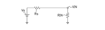
- FIG. 4 is an equivalent circuit diagram including the equivalent input resistance RIN of the analog-to-digital conversion circuit 100 of FIG. 1, the signal source voltage Vs, and the signal source resistance Rs.
- the input node VIN of FIG. 4 corresponds to the input nodes VINP and VINN of FIG.
- the equivalent input resistance RIN is connected between the input node VI and the reference potential node.
- the signal source voltage Vs is the voltage of the signal source of the input voltage of the input node VIN.
- the signal source resistance Rs is the resistance of the signal source of the input voltage of the input node VI.
- the equivalent input resistance RIN is connected in series with the signal source resistance Rs.
- the voltage of the input node VIN is a voltage obtained by dividing the signal source voltage Vs by the signal source resistance Rs and the equivalent input resistance RIN. Therefore, if the equivalent input resistance RIN is sufficiently high, the voltage of the input node VIN becomes substantially the same as the signal source voltage Vs, and the conversion result of the analog-digital conversion circuit 100 becomes an appropriate value.
- the equivalent input resistance RIN when the equivalent input resistance RIN is low, the voltage of the input node VIN becomes lower than the signal source voltage Vs, and the conversion result of the analog-digital conversion circuit 110 becomes small. Therefore, it is desirable that the equivalent input resistance RIN is sufficiently high.
- the amount of charge charged by the capacitors CP and CN from the input nodes VINP and VINN is the amount of charge of the capacitors CP and CN based on the input voltage of the input nodes VINP and VINN of the previous sampling operation, and this time. It is a difference between the charge amounts of the capacitors CP and CN based on the input voltages of the input nodes VINP and VINN of the sampling operation. Therefore, since the amount of charge charged by the capacitors CP and CN from the input nodes VINP and VINN is small, the equivalent input resistance RIN of the analog-to-digital conversion circuit 100 can be sufficiently increased, and the sampling operation time can be shortened. can.
- step S201 a case where the charge amounts of the capacitors CP and CN are reset to 0 in step S201 will be described.
- step S202 the capacitors CP and CN start charging from the state where the charge amount is 0. Therefore, since the amount of charge charged by the capacitors CP and CN from the input nodes VINP and VINN increases, the equivalent input resistance RIN of the analog-to-digital conversion circuit 100 becomes low, and the sampling operation time becomes long.
- the sampling operation in step S202 will be described.
- the total capacitance value of the capacitors CN0A and CN0 to CN4 is also 32C, which is the same as the total capacitance value of the capacitors CP0A and CP0 to CP4.
- VINP and VINN represent the potential of the input node VINP and the potential of the input node VINN, respectively.
- the charge amount QSAMPP stored in the top nodes TOPP of the capacitors CP0A and CP0 to CP4 is represented by the equation (1).
- the charge amount QSAMPN stored in the top nodes TOPN of the capacitors CN0A and CN0 to CN4 is represented by the equation (2).
- QSAMPN -32C (-VINP + VINN) / 2 ...
- step S203 of FIG. 2 the analog-to-digital conversion circuit 100 performs a sequential comparison operation.
- the switch circuit SW5 is turned off.
- the switch circuits SW1 and SW2 are also turned off.
- the switch circuit SW5 is turned off first, the top node TOPP and TOPN are in a floating state, so that the charges of the top node TOPP of the capacitors CP0A and CP0 to CP4 and the top node TOPN of the capacitors CN0A and CN0 to CN4 are stored. Will be done.
- the switch circuits SP0A and SP0 to SP4 are in a floating state.
- the switch circuits SN0A and SN0 to SN4 are also in a floating state.
- the switch circuit SW3 is turned on.
- the switch circuits SW10 and SW11 are turned off.
- the switch circuits SW8 and SW9 are turned on. This prepares for sequential comparison by the comparator CMP.
- the switch circuits SW10 and SW11 apply a bias voltage of 1.5 V of the bias voltage node VCM to the comparison input nodes CIP and CIN of the comparator CMP during the sampling operation.
- the switch circuit SP4 connects the first terminal of the capacitor CP4 to the reference voltage node Vrefp.
- the switch circuit SN4 connects the third terminal of the capacitor CN4 to the reference voltage node Vrefn.
- the switch circuits SP0 to SP3 are connected to the reference voltage node Vrefp if the bit of the corresponding digital code is 1, and are connected to the reference voltage node Vrefn if the bit of the corresponding digital code is 0.
- the switch circuit SP0A that generates the 1-bit addition value is connected to the reference voltage node Vrefn (corresponding to the bit value "0" of the digital code). This is because it is not necessary to generate 2's complement data.
- the switch circuit SP0A is connected to the reference voltage node Vrefn.
- the switch circuit SN0A is connected to the reference voltage node Vrefp.
- VINP> VINN Since VINP> VINN is assumed, the comparison with the comparator CMP starts from, for example, VINP> VINN and the comparison with the reference voltage / 2, and if (VINP-VINN) is larger than the reference voltage / 2, the reference voltage. Compare ⁇ 3/4 with (VINP-VINN). If (VINP-VINN) is smaller than the reference voltage / 2, the reference voltage ⁇ 1/4 and (VINP-VINN) are compared. Further, if (VINP-VINN) is larger than the reference voltage ⁇ 1/4, the reference voltage ⁇ 3/8 and (VINP-VINN) are compared. Alternatively, if (VINP-VINN) is smaller than the reference voltage ⁇ 1/4, the reference voltage ⁇ 1/8 and (VINP-VINN) are compared.
- the switch circuit SP4 is connected to the reference voltage node Vref.
- the switch circuits SP0 to SP2 and SP0A are connected to the reference voltage node Vrefn.
- the switch circuit SP3 is connected to the reference voltage node Vref.
- the first terminal of the total capacitance value 8C of the capacitors CP0A and CP0 to CP2 is connected to the reference voltage node Vrefn.
- the first terminal of the total capacitance value 24C of the capacitors CP3 and CP4 is connected to the reference voltage node Vrefp.
- Vref and Vrefn represent the potentials of the reference voltage nodes Vrefp and Vrefn, respectively.
- -24C (Vref-Vtp) + 8C (Vtp-Vrefn) -32C (VINP-VINN) / 2
- Vtp -(VINP-VINN) / 2+ (Vref + Vrefn) / 2+ (Vref-Vrefn) / (2 ⁇ 2) ...
- the switch circuit SN4 is connected to the reference voltage node Vrefn.
- the switch circuits SN0 to SN2 and CN0A are connected to the reference voltage node Vrefp.
- the switch circuit SN3 is connected to the reference voltage node Vrefn.
- the third terminal of the total capacitance value 8C of the capacitors CN0A and CN0 to CN2 is connected to the reference voltage node Vrefp.
- the third terminal of the total capacitance value 24C of the capacitors CN3 and CN4 is connected to the reference voltage node Vrefn. Since the charge amount QSAMPN of the formula (2) is stored, the potential Vtn of the top node TOPN at this time is given by the formula (4).
- the potential of the comparative input node CIP becomes the potential Vtp.
- the potential of the comparative input node CIN becomes the potential Vtn.
- the comparator CMP outputs the difference potential Vtp-Vtn between the potential Vtp and the potential Vtun as the output signal CPO.
- Vtp-Vtn -(VINP-VINN) + (Vref-Vrefn) / 2 ... (5)
- the comparator CMP outputs the magnitude relationship between (VINP-VINN) and (Vref-Vrefn) / 2 as an output signal CPO.
- the control circuit SAR determines the most significant bit of the digital code to be "1" if (VINP-VINN) is (Vref-Vrefn) / 2 or more based on the output signal CPO. Further, the control circuit SAR determines the most significant bit of the digital code to be "0" if (VINP-VINN) is smaller than (Vref-Vrefn) / 2 based on the output signal CPO.
- the most significant bit of the digital code corresponds to the switch circuits SP3 and SN3.
- (VINP-VINN) is (Vref-Vrefn) / 2 or more.
- the comparator CMP compares (VINP-VINN) and (Vref-Vrefn) ⁇ 3/4, examines the magnitude relationship thereof, and narrows the range of the value of (VINP-VINN).
- the switch circuit SP4 is connected to the reference voltage node Vref.
- the switch circuits SP0A, SP0 and SP1 are connected to the reference voltage node Vrefn.
- the switch circuits SP2 and SP3 are connected to the reference voltage node Vref.
- the first terminal of the total capacitance value 4C of the capacitors CP0A, CP0 and CP1 is connected to the reference voltage node Vrefn.
- the first terminal of the total capacitance value 28C of the capacitors CP2 to CP4 is connected to the reference voltage node Vrefp.
- the potential Vtp of the top node TOPP at this time is given by the equation (6).
- Vref-Vtp 4C
- Vtp-Vrefn -32C
- VINP-VINN 2+ (Vref + Vrefn) / 2 + 3 ⁇ (Vref-Vrefn) / (2 ⁇ 4) ... (6)
- the switch circuit SN4 is connected to the reference voltage node Vrefn.
- the switch circuits SN0A, SN0 and SN1 are connected to the reference voltage node Vref.
- the switch circuits SN2 and SN3 are connected to the reference voltage node Vrefn.
- the third terminal of the total capacitance value 4C of the capacitors CN0A, CN0 and CN1 is connected to the reference voltage node Vrefp.
- the third terminal of the total capacitance value 28C of the capacitors CN2 to CN4 is connected to the reference voltage node Vrefn.
- the potential Vtn of the top node TOPN at this time is given by the equation (7).
- Vref-Vtp 28C
- Vtp-Vrefn 32C
- Vtn (VINP-VINN) / 2+ (Vref + Vrefn) / 2-3 ⁇ (Vref-Vrefn) / (2 ⁇ 4) ... (7)
- Vtp-Vtn -(VINP-VINN) +3 ⁇ (Vref-Vrefn) / 4 ... (8)
- the comparator CMP outputs the magnitude relationship between (VINP-VINN) and (Vref-Vrefn) ⁇ 3/4 as an output signal CPO.
- the control circuit SAR determines the second high-order bit of the digital code to be "1" if (VINP-VINN) is (Vref-Vrefn) ⁇ 3/4 or more. Further, the control circuit SAR determines the second most significant bit of the digital code to be "0" if (VINP-VINN) is smaller than (Vref-Vrefn) ⁇ 3/4 based on the output signal CPO.
- the second high-order bit of the digital code corresponds to the switch circuits SP2 and SN2.
- control circuit SAR controls the switch circuits SP0A and SP0 to SP4 and the switch circuits SN0A and SN0 to SN4, and determines the magnitude relationship between the potentials obtained by dividing (VINP-VINN) and (Vref-Vref). can do.
- the control circuit SAR can sequentially narrow the range of (VINP-VINN) and determine the final digital code.
- the analog-to-digital conversion circuit 100 returns to step S201 after step S203 in FIG. 2, and repeats steps S201 to S203.
- the capacitors CP and CN do not reset the charge amount to 0, but distribute the initial charge.
- the amount of charge charged by the capacitors CP and CN from the input nodes VINP and VINN is the amount of charge of the capacitors CP and CN based on the input voltage of the input nodes VINP and VINN of the previous sampling operation, and this time. It is a difference between the charge amounts of the capacitors CP and CN based on the input voltages of the input nodes VINP and VINN of the sampling operation. Therefore, since the amount of charge charged by the capacitors CP and CN from the input nodes VINP and VINN is small, the equivalent input resistance RIN of the analog-to-digital conversion circuit 100 can be sufficiently increased, and the sampling operation time can be shortened. can. As a result, deterioration of the accuracy of the conversion result of the analog-to-digital conversion circuit 100 can be suppressed.
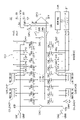
- FIG. 5 is a diagram showing a configuration example of the analog-to-digital conversion circuit 100 according to the second embodiment.
- the analog-to-digital conversion circuit 100 of FIG. 5 has, with respect to the analog-to-digital conversion circuit 100 of FIG. -CND, switch circuit SW4, and register file (memory) RF are added.
- the switch circuit SP0'and the capacitor CP0' in FIG. 5 are provided in place of the switch circuit SP0A and the capacitor CP0A in FIG.
- the relative capacitance value of the capacitor CP0' is 1C.
- the switch circuit SP0' connects the first terminal of the capacitor CP0' to the resistor sub-digital-to-analog conversion circuit SUBDACP, the bottom node BTP, the reference voltage node Vref, or Vrefn.
- the switch circuit SN0'and the capacitor CN0' in FIG. 5 are provided in place of the switch circuit SN0A and the capacitor CN0A in FIG.
- the relative capacitance value of the capacitor CN0' is 1C.
- the switch circuit SN0' connects the third terminal of the capacitor CN0' to the resistor sub-digital-to-analog conversion circuit SUBDACN, the bottom node BTN, the reference voltage node Vref, or Vrefn.
- the switch circuits SP0 to SP7 and capacitors CP0 to CP7 in FIG. 5 are provided in place of the switch circuits SP0 to SP4 and capacitors CP0 to CP4 in FIG.
- the switch circuits SN0 to SN7 and the capacitors CN0 to CN7 of FIG. 5 are provided in place of the switch circuits SN0 to SN4 and the capacitors CN0 to CN4 of FIG.
- These are 7-bit capacitive main digital-to-analog conversion circuits MAINDAC with positive and negative signs, and are the same as those of the first embodiment.
- the analog-to-digital conversion circuit 100 is a 14-bit analog-to-digital conversion circuit that converts an analog input voltage into a 14-bit digital code.
- the 14-bit analog-to-digital conversion circuit 100 includes a 7-bit capacitance main digital-to-analog conversion circuit MAINDAC and 7-bit resistance sub-digital-to-analog conversion circuits SUBDACP and SUBDACN.
- the 7-bit capacity main digital-to-analog conversion circuit MAINDAC converts the digital code of the upper 7 bits of the 14 bits into an analog voltage.
- the 7-bit resistor sub-digital-to-analog conversion circuit SUBDACP and SUBDACN convert the digital code of the lower 7 bits of the 14 bits into an analog voltage.
- the analog-to-digital conversion circuit 100 further includes resistance-corrected digital-to-analog conversion circuits CALDACP and CALDACN.
- the resistance-corrected digital-to-analog conversion circuits CALDACP and CALDACN correct the manufacturing error of the capacitive main digital-to-analog conversion circuit MAINDAC.
- the analog-to-digital conversion circuit 100 can perform high-resolution analog-to-digital conversion.
- the resistance sub-digital-to-analog conversion circuit SUBDACP outputs the first analog voltage to the comparison input node CIP via the capacitors CPD and CP0'based on the lower 7-bit digital code of the 14-bit digital code.
- the resistor sub-digital-to-analog conversion circuit SUBDACN outputs a second analog voltage to the comparison input node CIN via the capacitors CND and CN0'based on the lower 7-bit digital code of the 14-bit digital code.
- the resistance correction digital-to-analog conversion circuit CALDACP is connected to the comparison input node CIP via the capacitors CPA to CPC, and corrects the voltages of the capacitors CP0'and CP0 to CP7.
- the resistance correction digital-to-analog conversion circuit CALDACN is connected to the comparison input node CIN via the capacitors CNA to CNC, and corrects the voltages of the capacitors CN0'and CN0 to CN7.
- the capacitance main digital-to-analog conversion circuit MAINDAC is responsible for determining the upper 7 bits and the positive / negative code bits among the conversion resolution of 14 bits and the positive / negative code bits, and the lower 7 bits are determined by the resistor.
- Sub-digital-to-analog conversion circuits SUBDACP and SUBDACN are responsible.
- the resistance sub-digital-to-analog conversion circuits SUBDACP and SUBDACN have two voltage outputs divided into upper bits and lower bits by resistance division in order to reduce the time constant of the output node and speed up the operation. ing.
- the voltage output of the upper bit of the resistance sub-digital-to-analog conversion circuit SUBDACP is connected to the top node TOPP via the capacitor CP0', and the voltage output of the lower bit of the resistance sub-digital-to-analog conversion circuit SUBDACP is connected via the capacitor CPD. It is connected to the comparison input node CIP.
- the voltage output of the upper bit of the resistor sub-digital-to-analog conversion circuit SUBDACN is connected to the top node TOPN via the capacitor CN0'. Further, the voltage output of the lower bit of the resistance sub-digital-to-analog conversion circuit SUBDACN is connected to the comparison input node CIN via the capacitor CND.
- analog-to-digital conversion circuit 100 in addition to the capacitance main digital-to-analog conversion circuit MAINDAC for performing 14-bit conversion and the resistance sub-digital-to-analog conversion circuits SUBDACP and SUBDACN, 9-bit resistance correction for canceling the capacitor mismatch.
- Digital-to-analog conversion circuits CALDACP and CALDACN are provided.
- the resistance correction digital-to-analog conversion circuits CALDACP and CALDACN are used to realize the self-correction function.
- the resistance correction digital-to-analog conversion circuit CALDACP is divided into three output voltages, each of which is connected to the comparison input node CIP via capacitors CPA to CPC. Further, the resistance correction digital-to-analog conversion circuit CALDACN is divided into three output voltages, each of which is connected to the comparison input node CIN via the capacitors CNA to CNC.
- the resistance correction digital-to-analog conversion circuits CALDACP and CALDACN have an extra 2 bits of resolution with respect to the resistance sub-digital-to-analog conversion circuits SUBDACP and SUBDACN, for example, the 14-bit 1LSB (least significant bit) of the analog-to-digital conversion.
- the 14-bit 1LSB least significant bit
- bits are determined from the upper side of the capacitive main digital-to-analog conversion circuit MAINDAC, as in the first embodiment. After the upper 7 bits of the capacitance main digital-to-analog conversion circuit MAINDAC are determined, the lower 7 bits are determined using the resistance sub-digital-to-analog conversion circuits SUBDACP and SUBDACN.
- the resistance correction digital-to-analog conversion circuits CALDACP and CALDACN operate so as to correct the capacitance main digital-to-analog conversion circuit MAINDAC.
- the resistance sub-digital-to-analog conversion circuits SUBDACP and SUBDACN have a voltage output of 4 bits for the upper part and a voltage output for 3 bits for the lower part.
- the resistance correction digital-to-analog conversion circuits CALDACP and CALDACN have a voltage output of 3 bits for the upper part, a voltage output for 3 bits for the middle part, and a voltage output for 3 bits for the lower part.
- the outputs of the resistance sub-digital-to-analog conversion circuits SUBDACP and SUBDACN and the resistance correction digital-to-analog conversion circuits CALDACP and CALDACN are divided and added to the capacitors.
- the time constants of the resistance sub-digital-to-analog conversion circuits SUBDACP and SUBDACN and the resistance correction digital-to-analog conversion circuits CALDACP and CALDACN are reduced, and the effect of speeding up can be obtained.
- the error of the capacitance main digital-to-analog conversion circuit MAINDAC measured by the capacitor mismatch measurement can be converted into the amount to be corrected (correction data) of the capacitor carrying each bit.
- the correction data is stored in the register file RF.
- step S203 In the stage of the sequential comparison operation in step S203, as described above, first, the trial and determination of the most significant bit are performed, then the trial and determination of the second bit from the upper order are performed, and further, the trial and determination of the second bit from the upper order are performed. The bitth trial and judgment are performed. After that, trial and determination are performed for each bit up to the least significant bit.
- the resistance correction digital-to-analog conversion circuit CALDACP and CALDACN calculate the correction amount according to the digital code input to the capacitance main digital-to-analog conversion circuit MAINDAC at each stage of the sequential comparison operation, and perform the correction.
- the operation of the error correction control will be described.
- the correction value corresponding to the capacitor carrying the most significant bit is output from the register file RF.
- the resistance-corrected digital analog CALDACP and CALDACN output a voltage based on the value of the register file RF.
- the comparator CMP finishes the determination and outputs "1" or "0".
- the determination of the most significant bit is "1"
- the most significant bit correction value of the register file RF is stored in the register. If it is "0”, the value of 0 is stored.
- the register file RF outputs the correction value of the capacitor that bears the second bit from the upper.
- the resistance correction digital analog CALDACP and CALDACN output a voltage based on the sum of the output value of the register file RF and the value of the register.
- the correction amount corresponding to the digital code of the capacity main digital-to-analog conversion circuit MAINDAC is input to the resistance correction digital-to-analog conversion circuits CALDACP and CALDACN.
- the high-order bit is determined by the capacitive main digital-to-analog conversion circuit MAINDAC
- the low-order bit is searched by the resistance sub-digital-to-analog conversion circuits SUBDACP and SUBDACN. Since the resistance sub-digital-to-analog conversion circuits SUBDACP and SUBDACN have a small weight with respect to the dynamic range of analog-to-digital conversion, they do not need to be corrected.
- the 14-bit analog-to-digital conversion circuit 100 includes a 7-bit capacitance main digital-to-analog conversion circuit MAINDAC, a 7-bit resistance sub-digital-to-analog conversion circuit SUBDACP, SUBDACN, and a 9-bit resistance correction digital-to-analog conversion circuit CALDACP. It has a CALDACN and can convert an input analog voltage into a 14-bit digital code.
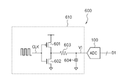
- FIG. 6 is a diagram showing a configuration example of the semiconductor integrated circuit 600 according to the third embodiment.
- the semiconductor integrated circuit 600 has an internal circuit 610 and an analog-to-digital conversion circuit 100.
- the analog-to-digital conversion circuit 100 is the analog-to-digital conversion circuit 100 of the first or second embodiment.
- the internal circuit 610 has a p-channel field-effect transistor 601, an n-channel field-effect transistor 602, a resistor 603, and a capacitor 604.
- the p-channel field-effect transistor 601 and the n-channel field-effect transistor 602 constitute an inverter.
- the resistor 603 and the capacitor 604 constitute a primary RC filter.
- the internal circuit 610 is, for example, a duty ratio measuring circuit for the clock signal CLK.
- the phase lock loop circuit PLL circuit
- the frequency of the clock signal CLK is high, for example, 12 GHz or the like.
- the clock signal CLK is transmitted from the PLL circuit to the supply destination circuit while being relayed by, for example, a CMOS inverter or a buffer.
- the duty ratio of the clock signal CLK deteriorates while being relayed.
- the duty ratio is the ratio of the period of one cycle of the clock signal to the period of high level.
- the duty ratio of the clock signal CLK is preferably 50%.
- the p-channel field-effect transistor 601 and the n-channel field-effect transistor 602 are inverters and shape the waveform of the clock signal CLK.
- the resistor 603 and the capacitor 604 are primary RC filters, smooth the output signal of the inverter, and output an analog DC voltage V1.
- the duty ratio of the clock signal CLK is 50%
- the DC voltage V1 becomes the average value of the high level and the low level of the clock signal CLK.
- the duty ratio of the clock signal CLK can be derived based on the DC voltage V1.
- the internal circuit 610 outputs an analog differential input voltage based on the DC voltage V1 to the analog-to-digital conversion circuit 100.
- the analog-to-digital conversion circuit 100 converts the differential input voltage based on the input voltage V1 into the digital code D1 as in the first or second embodiment.
- the resistance 603 is, for example, 20 k ⁇
- the capacitor 604 is, for example, 20 pF
- the signal source resistance Rs in FIG. 4 is high, for example, 100 k ⁇ . Therefore, if the equivalent input resistance RIN in FIG. 4 is low, the DC voltage V1 drops and an accurate duty ratio cannot be measured.
- the analog-to-digital conversion circuit 100 of the present embodiment has a sufficiently high equivalent input resistance RIN, it is possible to suppress a decrease in the DC voltage V1 and measure an accurate duty ratio.
Landscapes
- Engineering & Computer Science (AREA)
- Theoretical Computer Science (AREA)
- Physics & Mathematics (AREA)
- Nonlinear Science (AREA)
- Power Engineering (AREA)
- Analogue/Digital Conversion (AREA)
Priority Applications (3)
| Application Number | Priority Date | Filing Date | Title |
|---|---|---|---|
| PCT/JP2020/041165 WO2022097191A1 (ja) | 2020-11-04 | 2020-11-04 | サンプリング回路、アナログデジタル変換回路、及び半導体集積回路 |
| JP2022560532A JP7670995B2 (ja) | 2020-11-04 | 2020-11-04 | サンプリング回路、アナログデジタル変換回路、及び半導体集積回路 |
| US18/301,708 US12328128B2 (en) | 2020-11-04 | 2023-04-17 | Sampling circuit, analog-to-digital converter circuit, and semiconductor integrated circuit |
Applications Claiming Priority (1)
| Application Number | Priority Date | Filing Date | Title |
|---|---|---|---|
| PCT/JP2020/041165 WO2022097191A1 (ja) | 2020-11-04 | 2020-11-04 | サンプリング回路、アナログデジタル変換回路、及び半導体集積回路 |
Related Child Applications (1)
| Application Number | Title | Priority Date | Filing Date |
|---|---|---|---|
| US18/301,708 Continuation US12328128B2 (en) | 2020-11-04 | 2023-04-17 | Sampling circuit, analog-to-digital converter circuit, and semiconductor integrated circuit |
Publications (1)
| Publication Number | Publication Date |
|---|---|
| WO2022097191A1 true WO2022097191A1 (ja) | 2022-05-12 |
Family
ID=81457592
Family Applications (1)
| Application Number | Title | Priority Date | Filing Date |
|---|---|---|---|
| PCT/JP2020/041165 Ceased WO2022097191A1 (ja) | 2020-11-04 | 2020-11-04 | サンプリング回路、アナログデジタル変換回路、及び半導体集積回路 |
Country Status (3)
| Country | Link |
|---|---|
| US (1) | US12328128B2 (https=) |
| JP (1) | JP7670995B2 (https=) |
| WO (1) | WO2022097191A1 (https=) |
Citations (6)
| Publication number | Priority date | Publication date | Assignee | Title |
|---|---|---|---|---|
| JPS6468022A (en) * | 1987-08-11 | 1989-03-14 | Texas Instruments Inc | Differential analog/digital converter and method of analog/digital conversion |
| JP2001267925A (ja) * | 2000-03-17 | 2001-09-28 | Matsushita Electric Ind Co Ltd | 逐次比較型ad変換器 |
| WO2007058011A1 (ja) * | 2005-11-21 | 2007-05-24 | Matsushita Electric Industrial Co., Ltd. | 全差動型比較器及び全差動型増幅回路 |
| JP2011035944A (ja) * | 2010-11-15 | 2011-02-17 | Fujitsu Semiconductor Ltd | アナログデジタル変換器 |
| US9432044B1 (en) * | 2015-12-18 | 2016-08-30 | Texas Instruments Incorporated | Mismatch correction of attenuation capacitor in a successive approximation register analog to digital converter |
| JP2017079451A (ja) * | 2015-10-22 | 2017-04-27 | 株式会社ソシオネクスト | A/d変換器、a/d変換方法および半導体集積回路 |
Family Cites Families (7)
| Publication number | Priority date | Publication date | Assignee | Title |
|---|---|---|---|---|
| US4989002A (en) | 1990-02-12 | 1991-01-29 | Texas Instruments Incorporated | Common-mode error self-calibration circuit and method of operation |
| JP4652214B2 (ja) * | 2005-11-18 | 2011-03-16 | 富士通セミコンダクター株式会社 | アナログデジタル変換器 |
| JP5310222B2 (ja) | 2009-04-20 | 2013-10-09 | 富士通株式会社 | 電荷分配型デジタル・アナログ変換器及びそれを有する逐次比較型アナログ・デジタル変換器 |
| JP5427663B2 (ja) | 2010-03-24 | 2014-02-26 | スパンション エルエルシー | A/d変換器 |
| JP5561039B2 (ja) | 2010-09-03 | 2014-07-30 | 富士通株式会社 | アナログ・デジタル変換器およびシステム |
| US8581770B2 (en) | 2011-05-04 | 2013-11-12 | Texas Instruments Incorporated | Zero-power sampling SAR ADC circuit and method |
| JP5623618B2 (ja) | 2013-12-02 | 2014-11-12 | スパンションエルエルシー | A/d変換器 |
-
2020
- 2020-11-04 JP JP2022560532A patent/JP7670995B2/ja active Active
- 2020-11-04 WO PCT/JP2020/041165 patent/WO2022097191A1/ja not_active Ceased
-
2023
- 2023-04-17 US US18/301,708 patent/US12328128B2/en active Active
Patent Citations (6)
| Publication number | Priority date | Publication date | Assignee | Title |
|---|---|---|---|---|
| JPS6468022A (en) * | 1987-08-11 | 1989-03-14 | Texas Instruments Inc | Differential analog/digital converter and method of analog/digital conversion |
| JP2001267925A (ja) * | 2000-03-17 | 2001-09-28 | Matsushita Electric Ind Co Ltd | 逐次比較型ad変換器 |
| WO2007058011A1 (ja) * | 2005-11-21 | 2007-05-24 | Matsushita Electric Industrial Co., Ltd. | 全差動型比較器及び全差動型増幅回路 |
| JP2011035944A (ja) * | 2010-11-15 | 2011-02-17 | Fujitsu Semiconductor Ltd | アナログデジタル変換器 |
| JP2017079451A (ja) * | 2015-10-22 | 2017-04-27 | 株式会社ソシオネクスト | A/d変換器、a/d変換方法および半導体集積回路 |
| US9432044B1 (en) * | 2015-12-18 | 2016-08-30 | Texas Instruments Incorporated | Mismatch correction of attenuation capacitor in a successive approximation register analog to digital converter |
Also Published As
| Publication number | Publication date |
|---|---|
| JP7670995B2 (ja) | 2025-05-01 |
| JPWO2022097191A1 (https=) | 2022-05-12 |
| US20230261664A1 (en) | 2023-08-17 |
| US12328128B2 (en) | 2025-06-10 |
Similar Documents
| Publication | Publication Date | Title |
|---|---|---|
| US7928871B2 (en) | Successive approximation A/D converter | |
| US5534864A (en) | Pipelined analog-to-digital converter | |
| US8451151B2 (en) | Successive approximation analog to digital converter with capacitor mismatch calibration and method thereof | |
| CN108574487B (zh) | 逐次逼近寄存器模数转换器 | |
| US7928880B2 (en) | Digital analog converter | |
| JP5517898B2 (ja) | アナログデジタル変換器 | |
| US8957794B2 (en) | A/D converter and method for calibrating the same | |
| US11349492B2 (en) | Analog-to-digital converter | |
| US10218377B2 (en) | Gain calibration for ADC with external reference | |
| JP5482158B2 (ja) | 逐次比較a/d変換器 | |
| TWI783072B (zh) | 用於使用經減小電容器陣列數位轉類比轉換(dac)在連續近似暫存器(sar)類比轉數位轉換器(adc)中進行偏移校正之方法及設備 | |
| US7486218B2 (en) | Cyclic analog-to-digital converter | |
| JP2010263399A (ja) | A/d変換回路、電子機器及びa/d変換方法 | |
| CN110504971B (zh) | 基于储存电容器的模数转换器 | |
| US9606511B2 (en) | Analog/digital conversion circuit | |
| JP3857450B2 (ja) | 逐次比較型アナログ・ディジタル変換回路 | |
| CN106998206B (zh) | 电荷再分配连续逼近式模拟数字转换器及其控制方法 | |
| JPWO2016203522A1 (ja) | 逐次比較型a/d変換装置 | |
| CN118740150A (zh) | 可自动调校满刻度电压的逐次逼近模拟数字转换器及方法 | |
| US20110032128A1 (en) | Analog-digital converter circuit and calibration method | |
| JP7670995B2 (ja) | サンプリング回路、アナログデジタル変換回路、及び半導体集積回路 | |
| CN111342843B (zh) | 电压信号生成 | |
| US5646515A (en) | Ratioed reference voltage generation using self-correcting capacitor ratio and voltage coefficient error | |
| JP2015130587A (ja) | A/d変換器およびa/d変換方法 | |
| JPH09266446A (ja) | アナログ・デジタル変換器及びそれを内蔵したシングルチップ・マイクロコンピュータ |
Legal Events
| Date | Code | Title | Description |
|---|---|---|---|
| 121 | Ep: the epo has been informed by wipo that ep was designated in this application |
Ref document number: 20960745 Country of ref document: EP Kind code of ref document: A1 |
|
| ENP | Entry into the national phase |
Ref document number: 2022560532 Country of ref document: JP Kind code of ref document: A |
|
| NENP | Non-entry into the national phase |
Ref country code: DE |
|
| 122 | Ep: pct application non-entry in european phase |
Ref document number: 20960745 Country of ref document: EP Kind code of ref document: A1 |