WO2022092202A1 - 積層フィルム、第2積層フィルムの製造方法およびひずみセンサの製造方法 - Google Patents
積層フィルム、第2積層フィルムの製造方法およびひずみセンサの製造方法 Download PDFInfo
- Publication number
- WO2022092202A1 WO2022092202A1 PCT/JP2021/039823 JP2021039823W WO2022092202A1 WO 2022092202 A1 WO2022092202 A1 WO 2022092202A1 JP 2021039823 W JP2021039823 W JP 2021039823W WO 2022092202 A1 WO2022092202 A1 WO 2022092202A1
- Authority
- WO
- WIPO (PCT)
- Prior art keywords
- laminated film
- resistance
- resistance layer
- heating
- strain sensor
- Prior art date
- Legal status (The legal status is an assumption and is not a legal conclusion. Google has not performed a legal analysis and makes no representation as to the accuracy of the status listed.)
- Ceased
Links
Images

Classifications
-
- G—PHYSICS
- G01—MEASURING; TESTING
- G01B—MEASURING LENGTH, THICKNESS OR SIMILAR LINEAR DIMENSIONS; MEASURING ANGLES; MEASURING AREAS; MEASURING IRREGULARITIES OF SURFACES OR CONTOURS
- G01B7/00—Measuring arrangements characterised by the use of electric or magnetic techniques
- G01B7/16—Measuring arrangements characterised by the use of electric or magnetic techniques for measuring the deformation in a solid, e.g. by resistance strain gauge
- G01B7/18—Measuring arrangements characterised by the use of electric or magnetic techniques for measuring the deformation in a solid, e.g. by resistance strain gauge using change in resistance
-
- B—PERFORMING OPERATIONS; TRANSPORTING
- B32—LAYERED PRODUCTS
- B32B—LAYERED PRODUCTS, i.e. PRODUCTS BUILT-UP OF STRATA OF FLAT OR NON-FLAT, e.g. CELLULAR OR HONEYCOMB, FORM
- B32B9/00—Layered products comprising a layer of a particular substance not covered by groups B32B11/00 - B32B29/00
-
- C—CHEMISTRY; METALLURGY
- C23—COATING METALLIC MATERIAL; COATING MATERIAL WITH METALLIC MATERIAL; CHEMICAL SURFACE TREATMENT; DIFFUSION TREATMENT OF METALLIC MATERIAL; COATING BY VACUUM EVAPORATION, BY SPUTTERING, BY ION IMPLANTATION OR BY CHEMICAL VAPOUR DEPOSITION, IN GENERAL; INHIBITING CORROSION OF METALLIC MATERIAL OR INCRUSTATION IN GENERAL
- C23C—COATING METALLIC MATERIAL; COATING MATERIAL WITH METALLIC MATERIAL; SURFACE TREATMENT OF METALLIC MATERIAL BY DIFFUSION INTO THE SURFACE, BY CHEMICAL CONVERSION OR SUBSTITUTION; COATING BY VACUUM EVAPORATION, BY SPUTTERING, BY ION IMPLANTATION OR BY CHEMICAL VAPOUR DEPOSITION, IN GENERAL
- C23C14/00—Coating by vacuum evaporation, by sputtering or by ion implantation of the coating forming material
- C23C14/06—Coating by vacuum evaporation, by sputtering or by ion implantation of the coating forming material characterised by the coating material
- C23C14/0641—Nitrides
-
- C—CHEMISTRY; METALLURGY
- C23—COATING METALLIC MATERIAL; COATING MATERIAL WITH METALLIC MATERIAL; CHEMICAL SURFACE TREATMENT; DIFFUSION TREATMENT OF METALLIC MATERIAL; COATING BY VACUUM EVAPORATION, BY SPUTTERING, BY ION IMPLANTATION OR BY CHEMICAL VAPOUR DEPOSITION, IN GENERAL; INHIBITING CORROSION OF METALLIC MATERIAL OR INCRUSTATION IN GENERAL
- C23C—COATING METALLIC MATERIAL; COATING MATERIAL WITH METALLIC MATERIAL; SURFACE TREATMENT OF METALLIC MATERIAL BY DIFFUSION INTO THE SURFACE, BY CHEMICAL CONVERSION OR SUBSTITUTION; COATING BY VACUUM EVAPORATION, BY SPUTTERING, BY ION IMPLANTATION OR BY CHEMICAL VAPOUR DEPOSITION, IN GENERAL
- C23C14/00—Coating by vacuum evaporation, by sputtering or by ion implantation of the coating forming material
- C23C14/22—Coating by vacuum evaporation, by sputtering or by ion implantation of the coating forming material characterised by the process of coating
- C23C14/34—Sputtering
-
- C—CHEMISTRY; METALLURGY
- C23—COATING METALLIC MATERIAL; COATING MATERIAL WITH METALLIC MATERIAL; CHEMICAL SURFACE TREATMENT; DIFFUSION TREATMENT OF METALLIC MATERIAL; COATING BY VACUUM EVAPORATION, BY SPUTTERING, BY ION IMPLANTATION OR BY CHEMICAL VAPOUR DEPOSITION, IN GENERAL; INHIBITING CORROSION OF METALLIC MATERIAL OR INCRUSTATION IN GENERAL
- C23C—COATING METALLIC MATERIAL; COATING MATERIAL WITH METALLIC MATERIAL; SURFACE TREATMENT OF METALLIC MATERIAL BY DIFFUSION INTO THE SURFACE, BY CHEMICAL CONVERSION OR SUBSTITUTION; COATING BY VACUUM EVAPORATION, BY SPUTTERING, BY ION IMPLANTATION OR BY CHEMICAL VAPOUR DEPOSITION, IN GENERAL
- C23C14/00—Coating by vacuum evaporation, by sputtering or by ion implantation of the coating forming material
- C23C14/58—After-treatment
- C23C14/5806—Thermal treatment
-
- C—CHEMISTRY; METALLURGY
- C23—COATING METALLIC MATERIAL; COATING MATERIAL WITH METALLIC MATERIAL; CHEMICAL SURFACE TREATMENT; DIFFUSION TREATMENT OF METALLIC MATERIAL; COATING BY VACUUM EVAPORATION, BY SPUTTERING, BY ION IMPLANTATION OR BY CHEMICAL VAPOUR DEPOSITION, IN GENERAL; INHIBITING CORROSION OF METALLIC MATERIAL OR INCRUSTATION IN GENERAL
- C23C—COATING METALLIC MATERIAL; COATING MATERIAL WITH METALLIC MATERIAL; SURFACE TREATMENT OF METALLIC MATERIAL BY DIFFUSION INTO THE SURFACE, BY CHEMICAL CONVERSION OR SUBSTITUTION; COATING BY VACUUM EVAPORATION, BY SPUTTERING, BY ION IMPLANTATION OR BY CHEMICAL VAPOUR DEPOSITION, IN GENERAL
- C23C14/00—Coating by vacuum evaporation, by sputtering or by ion implantation of the coating forming material
- C23C14/58—After-treatment
- C23C14/5873—Removal of material
Definitions
- the present invention relates to a laminated film, a method for manufacturing a second laminated film, and a method for manufacturing a strain sensor. Specifically, the present invention relates to a laminated film, a method for manufacturing a second laminated film using the laminated film, and a manufacturing method for a strain sensor using the laminated film. Regarding the method.
- Patent Document 1 first, a Cr—N thin film is formed on the surface of an insulating substrate to prepare a thin film laminated film, and then heat treatment is performed at 300 ° C. to pattern the Cr—N thin film to manufacture a strain sensor. ing.
- the absolute value of the temperature coefficient of resistance (TCR) of the Cr—N thin film is reduced by heat treatment at 300 ° C., and the stability of the strain sensor is improved.
- a hard silicon substrate is used as an insulating substrate that can withstand the above-mentioned high-temperature heat treatment.
- the base material made of a resin having low heat resistance cannot be heat-treated at the above-mentioned temperature, and the absolute value of the temperature coefficient of resistance may not be reduced.
- the present invention relates to a laminated film capable of forming a resistance layer having a low absolute value of the temperature coefficient of resistance even when heated at a low temperature, a method for manufacturing a second laminated film using the laminated film, and a strain sensor using the laminated film. To provide a manufacturing method for.
- an insulating base resin film and a resistance layer are provided in order in the thickness direction, the resistance layer contains chromium nitride, and the temperature coefficient of resistance of the resistance layer is ⁇ 400 ppm / ° C. or higher. It is a laminated film having a temperature of ⁇ 200 ppm / ° C. or lower.
- the present invention [2] includes the laminated film according to the above [1], wherein the resistance layer has a body-centered cubic lattice structure.
- the present invention [3] includes the laminated film according to the above [1] or [2], wherein the resistance layer does not have an A15 type structure.
- the present invention [4] is any one of the above [1] to [3], wherein the molar portion of the nitrogen atom with respect to 100 mol parts of the chromium atom is 3.0 mol parts or more and less than 9 mol parts in the chromium nitride.
- the laminated film according to one item is included.
- the present invention [5] includes the laminated film according to any one of the above [1] to [4], wherein the thickness of the resistance layer is 10 nm or more and 150 nm or less.
- the present invention [6] includes the laminated film according to any one of the above [1] to [5], wherein the base resin film has a thickness of 10 ⁇ m or more and 200 ⁇ m or less.
- the present invention [7] includes the laminated film according to any one of the above [1] to [6], wherein the material of the base resin film is polyimide.
- the present invention [8] includes a preparatory step for preparing the laminated film according to any one of the above [1] to [7], and a heating step for heating the laminated film at 200 ° C. or lower.
- 2 Includes a method for manufacturing a laminated film.
- the present invention includes a preparatory step for preparing the laminated film according to any one of the above [1] to [7], a heating step for heating the laminated film at 200 ° C. or lower, and the laminated film.
- the present invention comprises a method of manufacturing a strain sensor, comprising a patterning step of patterning the resistance layer in the above.
- the laminated film of the present invention includes a resistance layer having a predetermined temperature coefficient of resistance. Therefore, even if this laminated film is heated at a low temperature, a resistance layer having a low absolute value of the temperature coefficient of resistance can be formed.
- the method for producing the second laminated film of the present invention is to produce the second laminated film using the laminated film of the present invention. Therefore, it is possible to form a resistance layer having a low absolute value of the temperature coefficient of resistance even when heated at a low temperature.
- the method for manufacturing a strain sensor of the present invention uses the laminated film of the present invention to manufacture a strain sensor. Therefore, a strain sensor having excellent stability can be obtained.
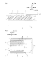
- FIG. 1 is a cross-sectional view of an embodiment of the laminated film of the present invention.
- 2A and 2B are strain sensors in which the resistance layer shown in FIG. 1 is patterned, FIG. 2A is a cross-sectional view, and FIG. 2B is a plan view.
- the laminated film 1 is used for manufacturing a second laminated film described later and a strain sensor 15 (see FIGS. 2A to 2B) described later.
- This laminated film 1 is independently distributed as a precursor of the second laminated film and the strain sensor 15.
- the laminated film 1 has a flat plate shape extending in a plane direction orthogonal to the thickness direction. Specifically, the laminated film 1 includes a base resin film 2 and a resistance layer 3 in order toward one side in the thickness direction. Specifically, the laminated film 1 includes a base resin film 2 and a resistance layer 3 arranged on one surface of the base resin film 2.
- the base resin film 2 is insulating.
- the base resin film 2 forms the other side of the laminated film 1 in the thickness direction.
- the base material resin film 2 has a flat plate shape extending in the plane direction.
- the material of the base resin film examples include resins such as polyimide, polyester, polyethylene terephthalate, and polyethylene naphthalate.
- the material of the base resin film 2 is preferably polyimide. If the base resin film 2 is polyimide, it can be heated up to 200 ° C.
- the coefficient of linear expansion of the base material resin film 2 is, for example, 30 ppm / ° C. or less, preferably 15 ppm / ° C. or less.
- the thickness of the base resin film 2 is not particularly limited, and is, for example, 2 ⁇ m or more, preferably 10 ⁇ m or more, more preferably 20 ⁇ m or more, and for example, 500 ⁇ m or less, from the viewpoint of suppressing the generation of wrinkles. It is preferably 300 ⁇ m or less, more preferably 200 ⁇ m or less from the viewpoint of roll-to-roll transport.
- a corona discharge treatment an ultraviolet irradiation treatment, a plasma treatment, a sputtering etching treatment, or the like can be applied to one surface of the base resin film 2 in the thickness direction.
- the number of the base resin films 2 in the laminated film 1 is not particularly limited and is preferably 1.
- the resistance layer 3 is a layer that is heated and patterned when the strain sensor 15 (see FIGS. 2A to 2B) is manufactured from the laminated film 1.
- the resistance layer 3 is arranged on one side of the base resin film 2 in the thickness direction.
- the resistance layer 3 forms one side of the laminated film 1 in the thickness direction. Specifically, the resistance layer 3 is in contact with all of one surface of the base resin film 2 in the thickness direction.
- the resistance layer 3 contains chromium nitride. Specifically, the material of the resistance layer 3 contains chromium nitride as a main component. On the other hand, the material of the resistance layer 3 is allowed to be mixed with unavoidable impurities, for example. The proportion of unavoidable impurities in the resistance layer 3 is, for example, 1 atomic% or less, preferably 0.1 atomic% or less, and more preferably 0.05 atomic% or less. Preferably, the resistance layer 3 is made of chromium nitride.
- the molar portion of the nitrogen atom with respect to 100 mol parts of the chromium atom is, for example, 3.0 mol parts or more, preferably 3.5 mol parts or more, and for example, 10 mol parts or less, preferably 10 parts or more. It is less than 9.0 mol parts, more preferably 8.0 mol parts or less, still more preferably 6.0 mol parts or less.
- the temperature coefficient of resistance of the resistance layer 3 (specifically, the temperature coefficient of resistance before heating, which will be described later) can be adjusted to a predetermined range described later.
- the temperature coefficient of resistance of the resistance layer 3 (specifically, the temperature coefficient of resistance before heating, which will be described later) can be adjusted to a predetermined range described later.
- the resistance layer 3 does not include the A15 structure as the crystal structure of chromium nitride and has a body-centered cubic lattice structure.
- the temperature coefficient of resistance of the resistance layer 3 (specifically, the temperature coefficient of resistance before heating, which will be described later) can be adjusted to a predetermined range described later.
- the crystallinity of the resistance layer 3 can be enhanced and the stability can be improved without heating at a high temperature in the heating step described later.
- the temperature coefficient of resistance of the resistance layer 3 (specifically, the temperature coefficient of resistance before heating) is ⁇ 400 ppm / ° C. or higher, preferably ⁇ 300 ppm / ° C. or higher, and ⁇ 200 ppm / ° C. or lower.
- the absolute value of the temperature coefficient of resistance (specifically, the temperature coefficient of resistance after heating) can be lowered even if the resistance layer 3 is heated at a low temperature. Therefore, a strain sensor 15 having excellent stability can be obtained.
- the absolute value of the temperature coefficient of resistance (specifically, the temperature coefficient of resistance after heating) can be lowered even if the resistance layer 3 is heated at a low temperature. not. Therefore, it is not possible to obtain a strain sensor 15 having excellent stability.
- the absolute value of the temperature coefficient of resistance (specifically, the temperature coefficient of resistance after heating) can be lowered even if the resistance layer 3 is heated at a low temperature. .. Therefore, a strain sensor 15 having excellent stability can be obtained.
- the absolute value of the temperature coefficient of resistance (specifically, the temperature coefficient of resistance after heating) cannot be lowered even if the resistance layer 3 is heated at a low temperature. .. Therefore, it is not possible to obtain a strain sensor 15 having excellent stability.
- the thickness of the resistance layer 3 is, for example, 5 nm or more, preferably 10 nm or more from the viewpoint of increasing the gauge ratio of the resistance layer 3, and 150 nm or less, for example, from the viewpoint of suppressing the generation of cracks in the resistance layer 3. It is preferably 120 nm or less.
- the number of resistance layers 3 in the laminated film 1 is not particularly limited, and is preferably 1. Specifically, the number of the resistance layers 3 with respect to one base resin film 2 is preferably 1.
- the laminated film 1 is formed by a roll-to-roll method.
- the resistance layer 3 is formed on one side of the base resin film 2 in the thickness direction.
- the film forming method include a sputtering method, a vacuum vapor deposition method, and an ion plating method. Sputtering methods are preferred, and reactive sputtering is more preferred.
- the target is composed of chromium, and a mixed gas of an inert gas such as argon and nitrogen is used as the sputtering gas.
- the number of parts by volume of nitrogen with respect to 100 parts by volume of the inert gas is, for example, 0.5 parts by volume or more and 15 parts by volume or less.
- the laminated film 1 provided with the base resin film 2 and the resistance layer 3 is produced.
- the laminated film 1 can be suitably used for manufacturing the second laminated film and the strain sensor.
- the second laminated film is obtained by heating the laminated film 1 (specifically, the resistance layer 3 in the laminated film 1). That is, the second laminated film is the laminated film 1 after heating.
- the method for manufacturing the second laminated film includes a preparatory step for preparing the laminated film 1 and a heating step for heating the laminated film 1 at a predetermined temperature.
- the laminated film 1 is prepared.
- the laminated film 1 (resistance layer 3) is heated in order to enhance the crystallinity of the resistance layer 3 and improve the stability.
- the heating temperature is a temperature at which the base resin film 2 is not damaged by heating, for example, 200 ° C. or lower, preferably 160 ° C. or lower, and for example, 80 ° C. or higher, preferably 100 ° C. or higher. , More preferably 120 ° C. or higher.
- the heating time is, for example, 20 minutes or more, preferably 50 minutes or more, and for example, 240 minutes or less, preferably 120 minutes or less.
- heating temperature is not more than the above upper limit, damage due to heating of the base resin film 2 can be suppressed.
- the absolute value of the temperature coefficient of resistance after heating of the resistance layer 3 can be reduced.
- the absolute value of the temperature coefficient of resistance after heating of the resistance layer 3 can be reduced.
- the temperature coefficient of resistance after heating of the resistance layer 3 is, for example, -100 ppm / ° C. or higher, preferably -80 ppm / ° C. or higher, more preferably -50 ppm / ° C. or higher, still more preferably -20 ppm. It is / ° C. or higher, and is, for example, 100 ppm / ° C. or lower, preferably 80 ppm / ° C. or lower, more preferably 50 ppm / ° C. or lower, still more preferably 20 ppm / ° C. or lower.
- the absolute value of the temperature coefficient of resistance after heating of the resistance layer 3 is, for example, 100 or less, preferably 80 or less, more preferably 50 or less, and further preferably 20 or less.
- the second laminated film is excellent in stability.
- the method for manufacturing the strain sensor 15 includes a preparatory step for preparing the laminated film 1, a heating step for heating the laminated film 1 at a predetermined temperature, and a patterning step for patterning the resistance layer 3 in the laminated film 1.
- the laminated film 1 is prepared.
- the laminated film 1 (resistance layer 3) is heated in order to enhance the crystallinity of the resistance layer 3 and improve the stability.
- the heating conditions are the same as the heating conditions in the heating step of the second laminated film manufacturing method described above, and the heating temperature is a temperature at which the base resin film 2 is not damaged by heating, for example, 200 ° C. or lower. It is preferably 160 ° C. or lower, and for example, 80 ° C. or higher, preferably 100 ° C. or higher, and more preferably 120 ° C. or higher.
- the heating time is, for example, 20 minutes or more, preferably 50 minutes or more, and for example, 240 minutes or less, preferably 120 minutes or less.
- heating temperature is not more than the above upper limit, damage due to heating of the base resin film 2 can be suppressed.
- the absolute value of the temperature coefficient of resistance after heating of the resistance layer 3 can be reduced.
- the absolute value of the temperature coefficient of resistance after heating of the resistance layer 3 can be reduced.
- the temperature coefficient of resistance after heating of the resistance layer 3 is, for example, -100 ppm / ° C. or higher, preferably -80 ppm / ° C. or higher, more preferably -50 ppm / ° C. or higher, still more preferably -20 ppm. It is / ° C. or higher, and is, for example, 100 ppm / ° C. or lower, preferably 80 ppm / ° C. or lower, more preferably 50 ppm / ° C. or lower, still more preferably 20 ppm / ° C. or lower.
- the absolute value of the temperature coefficient of resistance after heating of the resistance layer 3 is, for example, 100 or less, preferably 80 or less, more preferably 50 or less, and further preferably 20 or less.
- the strain sensor 15 is excellent in stability.
- the resistance layer 3 in the laminated film 1 is patterned to form the resistance pattern 4.
- the patterning of the resistance layer 3 include etching, and specific examples thereof include dry etching, wet etching, preferably dry etching, and more preferably laser etching.
- the resistance pattern 4 integrally includes the strain sensor unit 5, the terminal 6, and the wiring 7.
- the strain sensor unit 5 has a substantially knotted shape in a plan view. Specifically, the strain sensor unit 5 has a plurality of first lines 8, a plurality of first connection lines 9, and a plurality of second connection lines 10.
- Each of the plurality of first lines 8 extends along the first direction (direction included in the plane direction).
- the plurality of first lines 8 are aligned and arranged at intervals in the second direction (direction included in the plane direction and orthogonal to the first direction).
- the plurality of first connecting lines 9 connect one end of the first line 8 adjacent to the second direction in the first direction.
- the plurality of second connecting lines 10 connect the other ends of the first lines 8 adjacent to each other in the second direction in the first direction. When projected in the first direction, the first connecting line 9 and the second connecting line 10 are arranged alternately.
- the terminal 6 is separated from the strain sensor unit 5 in the plane direction.
- the terminal 6 has, for example, a land shape having a substantially rectangular shape in a plan view. Two terminals 6 are provided at intervals.
- the wiring 7 connects the two terminals 6 and both ends of the strain sensor unit 5.
- one conductive path is formed from one terminal 6 through one wiring 7, strain sensor unit 5, and other wiring 7 to the other terminal 6.
- the dimensions of the strain sensor unit 5 are appropriately set according to the application and purpose.
- the width of the first line 8, the first connecting line 9 and the second connecting line 10 is, for example, 1 ⁇ m or more, preferably 5 ⁇ m or more, more preferably 10 ⁇ m or more, and for example, 150 ⁇ m or less, preferably preferably. It is 100 ⁇ m or less, more preferably 70 ⁇ m or less.
- the shape of the base material resin film 2 is also appropriately set according to the application and purpose of the strain sensor 15, and becomes a desired dimension by, for example, external processing.
- the laminated film 1 of the strain sensor 15 is attached to the surface of the subject 20 via the adhesive layer 21. Further, the lead wire 23 is connected to the two terminals 6 via the conductive adhesive layer 22. The lead wire 23 is electrically connected to an external resistance measurement circuit (not shown).
- the resistance value of the strain sensor unit 5 changes. Based on this, the strain amount is calculated in the resistance measurement circuit.
- the strain amount of the subject 20 is calculated.
- the laminated film 1 includes a resistance layer 3 having a predetermined temperature coefficient of resistance. Therefore, even if this laminated film is heated at a low temperature, a resistance layer having a low absolute value of the temperature coefficient of resistance can be formed. Therefore, a strain sensor 15 having excellent stability can be obtained.
- the second laminated film is manufactured by using the laminated film 1. Therefore, the resistance layer 3 having a low absolute value of the temperature coefficient of resistance can be formed even when heated at a low temperature. Therefore, a strain sensor 15 having excellent stability can be obtained.
- the method for manufacturing the strain sensor 15 is to manufacture the strain sensor 15 using the laminated film 1. Therefore, a strain sensor 15 having excellent stability can be obtained.
- the heating timing is before the patterning of the resistance layer 3, but may be, for example, after the patterning of the resistance layer 3.
- the base material resin film 2 can include, for example, a functional layer (not shown) such as a hard coat layer, an easy-adhesive layer, and an antistatic layer on one side in the thickness direction thereof.
- a functional layer such as a hard coat layer, an easy-adhesive layer, and an antistatic layer on one side in the thickness direction thereof.
- strain sensor 15 can cover the strain sensor portion 5 and further include a cover layer 12 (one-dot chain line) made of resin.
- 1 is exemplified as a suitable number of resistance layers 3 in the laminated film 1, but for example, although not shown, it may be 2.
- each of the two resistance layers 3 is arranged on both sides of the base resin film 2 in the thickness direction. That is, in a preferred example of this modification, the number of resistance layers 3 with respect to one base resin film 2 is preferably 2.
- Examples and comparative examples are shown below, and the present invention will be described in more detail.
- the present invention is not limited to Examples and Comparative Examples.
- specific numerical values such as the compounding ratio (content ratio), physical property values, parameters, etc. used in the following description are described in the above-mentioned "form for carrying out the invention", and the compounding ratios corresponding to them (Substitute the upper limit value (value defined as “less than or equal to” or “less than”) or the lower limit value (value defined as "greater than or equal to” or “excess”) such as content ratio), physical property value, parameter, etc. be able to.
- Example 1 A base resin film 2 having a thickness of 38 ⁇ m made of polyimide having a linear expansion coefficient of 13 ppm / ° C. was prepared.
- the base resin film 2 was set on the roll-to-roll take-out roll and the take-up roll, and was set on the sputtering apparatus arranged between them.
- the inside of the sputtering apparatus is exhausted until the degree of vacuum becomes 1 ⁇ 10 -3 Pa or less, it is composed of chromium nitride by reactive pulse DC sputtering (pulse width: 1 ⁇ s, frequency: 100 kHz) under the following conditions.
- the resistance layer 3 was formed into a film.
- the target is made of metallic chromium.
- Target Metallic chrome, flat plate shape of 500 mm x 150 mm Power: 5 kW (Power density: 6.7 W / cm 2 ) Magnetic flux density (target surface): 30mT-100mT Substrate temperature: 150 ° C Sputtering gas: Mixed gas of argon and nitrogen Film formation pressure: 0.085 Pa The ratio of nitrogen gas was adjusted so that the ratio of the number of moles of nitrogen atom to the number of moles of chromium atom was as shown in Table 1.
- the laminated film 1 provided with the base resin film 2 and the resistance layer 3 was manufactured.
- the laminated film 1 was heated at 130 ° C. for 60 minutes.
- the laminated film 1 was cut into a size of 10 mm ⁇ 200 mm, and a resistance pattern 4 including a knot-shaped strain sensor portion 5, a terminal 6, and a wiring 7 was formed from the resistance layer 3 by laser patterning.
- the line width of the strain sensor unit 5 was 30 ⁇ m.
- the resistance of the resistance pattern 4 was adjusted to be about 10 k ⁇ , and the resistance of the strain sensor unit 5 was adjusted to be 30 times the resistance of the wiring 7. As a result, a strain sensor 15 was obtained.
- Example 2 to Example 6 Comparative Example 1 to Comparative Example 6
- the same treatment as in Example 1 was performed except that the ratio of the number of moles of nitrogen atoms to the number of moles of chromium atoms and the heating conditions were changed according to Table 1, to obtain a laminated film 1 and a strain sensor 15. .. Specifically, the ratio of nitrogen in the sputtering gas was adjusted.
- ⁇ Temperature coefficient of resistance> The temperatures of the resistance layer 3 of the laminated film 1 of each example and the comparative example and the strain sensor portion 5 of the strain sensor 15 were set to 5 ° C. A tester was connected to each of the two terminals 6, a constant current was passed, and the voltage was read to measure the two-terminal resistance at 5 ° C. Similarly, the two-terminal resistance at 25 ° C and 45 ° C was measured.
- the temperature coefficient of resistance calculated from the resistance values of 5 ° C. and 25 ° C. and the average value of the temperature coefficient of resistance calculated from the resistance values of 25 ° C. and 45 ° C. are calculated as the temperature coefficient of resistance of the resistance layer 3 of the laminated film 1. It was obtained as the temperature coefficient of resistance of the resistance layer 3 before heating) and the temperature coefficient of resistance of the strain sensor unit 5 (temperature coefficient of resistance of the resistance layer 3 after heating).
- Example 1 Although the ratio of nitrogen atom to chromium atom is the same in Example 1, Example 2, and Example 4, the resistance temperature coefficient of the resistance layer 3 before heating is different. Specifically, the temperature coefficient of resistance of the resistance layer 3 before heating has a variation of about ⁇ 16.
- Such a variation is due to a measurement error of the resistance value and an in-plane variation of the resistance layer 3, and is a variation to the extent that the effect of the present invention is not impaired.
- Example 3 The same applies to Example 3 and Example 4.
- the resistance layer 3 of Examples 1 to 6 does not have an A15 structure but has only a body-centered cubic lattice structure.
- the laminated film, the method for manufacturing the second laminated film, and the method for manufacturing the strain sensor of the present invention can be suitably used for manufacturing the strain sensor, for example.
Landscapes
- Chemical & Material Sciences (AREA)
- Chemical Kinetics & Catalysis (AREA)
- Engineering & Computer Science (AREA)
- Materials Engineering (AREA)
- Mechanical Engineering (AREA)
- Metallurgy (AREA)
- Organic Chemistry (AREA)
- Physics & Mathematics (AREA)
- General Physics & Mathematics (AREA)
- Thermal Sciences (AREA)
- Measurement Of Length, Angles, Or The Like Using Electric Or Magnetic Means (AREA)
- Laminated Bodies (AREA)
Priority Applications (2)
| Application Number | Priority Date | Filing Date | Title |
|---|---|---|---|
| CN202180072118.3A CN116438062A (zh) | 2020-10-30 | 2021-10-28 | 层叠薄膜、第2层叠薄膜的制造方法和应变传感器的制造方法 |
| US18/251,270 US20230408244A1 (en) | 2020-10-30 | 2021-10-28 | Laminated film, method for producing second laminated film, and method for producing strain sensor |
Applications Claiming Priority (2)
| Application Number | Priority Date | Filing Date | Title |
|---|---|---|---|
| JP2020182131A JP7736429B2 (ja) | 2020-10-30 | 2020-10-30 | 積層フィルム、第2積層フィルムの製造方法およびひずみセンサの製造方法 |
| JP2020-182131 | 2020-10-30 |
Publications (1)
| Publication Number | Publication Date |
|---|---|
| WO2022092202A1 true WO2022092202A1 (ja) | 2022-05-05 |
Family
ID=81383386
Family Applications (1)
| Application Number | Title | Priority Date | Filing Date |
|---|---|---|---|
| PCT/JP2021/039823 Ceased WO2022092202A1 (ja) | 2020-10-30 | 2021-10-28 | 積層フィルム、第2積層フィルムの製造方法およびひずみセンサの製造方法 |
Country Status (5)
| Country | Link |
|---|---|
| US (1) | US20230408244A1 (https=) |
| JP (2) | JP7736429B2 (https=) |
| CN (1) | CN116438062A (https=) |
| TW (1) | TW202225651A (https=) |
| WO (1) | WO2022092202A1 (https=) |
Families Citing this family (1)
| Publication number | Priority date | Publication date | Assignee | Title |
|---|---|---|---|---|
| JP2022150486A (ja) * | 2021-03-26 | 2022-10-07 | Tdk株式会社 | 歪抵抗膜、圧力センサおよび積層体 |
Citations (4)
| Publication number | Priority date | Publication date | Assignee | Title |
|---|---|---|---|---|
| JPH10270201A (ja) * | 1997-03-21 | 1998-10-09 | Res Inst Electric Magnetic Alloys | Cr−N基歪抵抗膜およびその製造法ならびに歪センサ |
| JP2014074661A (ja) * | 2012-10-04 | 2014-04-24 | Research Institute For Electromagnetic Materials | 歪ゲージ |
| JP2019066311A (ja) * | 2017-09-29 | 2019-04-25 | ミネベアミツミ株式会社 | ひずみゲージ |
| JP2020129013A (ja) * | 2020-06-05 | 2020-08-27 | ミネベアミツミ株式会社 | ひずみゲージ |
Family Cites Families (18)
| Publication number | Priority date | Publication date | Assignee | Title |
|---|---|---|---|---|
| JP2562610B2 (ja) * | 1987-08-08 | 1996-12-11 | 株式会社豊田中央研究所 | 歪ゲ−ジ用薄膜抵抗体 |
| CN1384914A (zh) | 1999-04-29 | 2002-12-11 | 罗得岛及普罗维登斯属地高等教育管理委员会 | 在高温下使用的自动补偿陶瓷应变计量器 |
| JP2018151204A (ja) | 2017-03-10 | 2018-09-27 | 公益財団法人電磁材料研究所 | 水素ガス環境用歪センサ |
| CN107331487B (zh) * | 2017-06-20 | 2019-04-09 | 华南理工大学 | 一种用于高温环境的TaN薄膜电阻及其制备方法 |
| JP2019066313A (ja) * | 2017-09-29 | 2019-04-25 | ミネベアミツミ株式会社 | ひずみゲージ |
| JP2019066454A (ja) * | 2017-09-29 | 2019-04-25 | ミネベアミツミ株式会社 | ひずみゲージ、センサモジュール |
| JP2019066312A (ja) * | 2017-09-29 | 2019-04-25 | ミネベアミツミ株式会社 | ひずみゲージ |
| JP2019066453A (ja) * | 2017-09-29 | 2019-04-25 | ミネベアミツミ株式会社 | ひずみゲージ |
| JP2019082424A (ja) * | 2017-10-31 | 2019-05-30 | ミネベアミツミ株式会社 | ひずみゲージ |
| JP2019090723A (ja) * | 2017-11-15 | 2019-06-13 | ミネベアミツミ株式会社 | ひずみゲージ |
| JP2019090724A (ja) * | 2017-11-15 | 2019-06-13 | ミネベアミツミ株式会社 | ひずみゲージ |
| JP2019113411A (ja) * | 2017-12-22 | 2019-07-11 | ミネベアミツミ株式会社 | ひずみゲージ、センサモジュール |
| JP2019132790A (ja) * | 2018-02-02 | 2019-08-08 | ミネベアミツミ株式会社 | ひずみゲージ |
| JP2019184344A (ja) * | 2018-04-05 | 2019-10-24 | ミネベアミツミ株式会社 | ひずみゲージ及びその製造方法 |
| JP2020053433A (ja) * | 2018-09-21 | 2020-04-02 | Koa株式会社 | 歪センサ抵抗器 |
| US11774303B2 (en) * | 2018-10-23 | 2023-10-03 | Minebea Mitsumi Inc. | Accelerator, steering wheel, six-axis sensor, engine, bumper and the like |
| JP7659380B2 (ja) | 2020-10-30 | 2025-04-09 | 日東電工株式会社 | 積層フィルムおよび歪みセンサの製造方法 |
| JP7698949B2 (ja) | 2020-10-30 | 2025-06-26 | 日東電工株式会社 | 積層フィルム、その製造方法およびひずみセンサ |
-
2020
- 2020-10-30 JP JP2020182131A patent/JP7736429B2/ja active Active
-
2021
- 2021-10-28 WO PCT/JP2021/039823 patent/WO2022092202A1/ja not_active Ceased
- 2021-10-28 CN CN202180072118.3A patent/CN116438062A/zh active Pending
- 2021-10-28 US US18/251,270 patent/US20230408244A1/en active Pending
- 2021-10-29 TW TW110140320A patent/TW202225651A/zh unknown
-
2025
- 2025-06-05 JP JP2025093877A patent/JP2025116237A/ja active Pending
Patent Citations (4)
| Publication number | Priority date | Publication date | Assignee | Title |
|---|---|---|---|---|
| JPH10270201A (ja) * | 1997-03-21 | 1998-10-09 | Res Inst Electric Magnetic Alloys | Cr−N基歪抵抗膜およびその製造法ならびに歪センサ |
| JP2014074661A (ja) * | 2012-10-04 | 2014-04-24 | Research Institute For Electromagnetic Materials | 歪ゲージ |
| JP2019066311A (ja) * | 2017-09-29 | 2019-04-25 | ミネベアミツミ株式会社 | ひずみゲージ |
| JP2020129013A (ja) * | 2020-06-05 | 2020-08-27 | ミネベアミツミ株式会社 | ひずみゲージ |
Also Published As
| Publication number | Publication date |
|---|---|
| JP7736429B2 (ja) | 2025-09-09 |
| CN116438062A (zh) | 2023-07-14 |
| US20230408244A1 (en) | 2023-12-21 |
| JP2022072602A (ja) | 2022-05-17 |
| JP2025116237A (ja) | 2025-08-07 |
| TW202225651A (zh) | 2022-07-01 |
Similar Documents
| Publication | Publication Date | Title |
|---|---|---|
| TWI841675B (zh) | 溫度感測膜、導電膜及其製造方法 | |
| JP2025116237A (ja) | 積層フィルム、第2積層フィルムの製造方法およびひずみセンサの製造方法 | |
| US12590855B2 (en) | Strain sensor, functional film, and method for manufacturing same | |
| WO2022092205A1 (ja) | 積層フィルム、その製造方法およびひずみセンサ | |
| WO2022092204A1 (ja) | 積層フィルムおよび歪みセンサ | |
| JP7659380B2 (ja) | 積層フィルムおよび歪みセンサの製造方法 | |
| TWI921402B (zh) | 積層膜、其製造方法及應變感測器 | |
| WO1986004989A1 (fr) | Element capteur de gaz compose d'un film d'oxide d'etain | |
| US12146799B2 (en) | Temperature sensor film, conductive film and method for producing same | |
| US12320715B2 (en) | Electroconductive film and temperature sensor film | |
| WO2022092203A1 (ja) | 歪みセンサーおよび積層体 | |
| TWI913349B (zh) | 積層膜及應變感測器 | |
| JP2018137268A (ja) | 電子デバイス及びその製造方法 | |
| JP7374589B2 (ja) | 温度センサフィルム、導電フィルムおよびその製造方法 |
Legal Events
| Date | Code | Title | Description |
|---|---|---|---|
| 121 | Ep: the epo has been informed by wipo that ep was designated in this application |
Ref document number: 21886319 Country of ref document: EP Kind code of ref document: A1 |
|
| NENP | Non-entry into the national phase |
Ref country code: DE |
|
| 122 | Ep: pct application non-entry in european phase |
Ref document number: 21886319 Country of ref document: EP Kind code of ref document: A1 |