WO2022080186A1 - 光学構造 - Google Patents
光学構造 Download PDFInfo
- Publication number
- WO2022080186A1 WO2022080186A1 PCT/JP2021/036799 JP2021036799W WO2022080186A1 WO 2022080186 A1 WO2022080186 A1 WO 2022080186A1 JP 2021036799 W JP2021036799 W JP 2021036799W WO 2022080186 A1 WO2022080186 A1 WO 2022080186A1
- Authority
- WO
- WIPO (PCT)
- Prior art keywords
- refractive index
- low refractive
- layer
- index layer
- optical structure
- Prior art date
- Legal status (The legal status is an assumption and is not a legal conclusion. Google has not performed a legal analysis and makes no representation as to the accuracy of the status listed.)
- Ceased
Links
Images





Classifications
-
- G—PHYSICS
- G02—OPTICS
- G02B—OPTICAL ELEMENTS, SYSTEMS OR APPARATUS
- G02B5/00—Optical elements other than lenses
- G02B5/18—Diffraction gratings
- G02B5/1866—Transmission gratings characterised by their structure, e.g. step profile, contours of substrate or grooves, pitch variations, materials
-
- G—PHYSICS
- G02—OPTICS
- G02B—OPTICAL ELEMENTS, SYSTEMS OR APPARATUS
- G02B1/00—Optical elements characterised by the material of which they are made; Optical coatings for optical elements
- G02B1/10—Optical coatings produced by application to, or surface treatment of, optical elements
-
- G—PHYSICS
- G02—OPTICS
- G02B—OPTICAL ELEMENTS, SYSTEMS OR APPARATUS
- G02B5/00—Optical elements other than lenses
- G02B5/18—Diffraction gratings
-
- G—PHYSICS
- G02—OPTICS
- G02B—OPTICAL ELEMENTS, SYSTEMS OR APPARATUS
- G02B5/00—Optical elements other than lenses
- G02B5/18—Diffraction gratings
- G02B5/1814—Diffraction gratings structurally combined with one or more further optical elements, e.g. lenses, mirrors, prisms or other diffraction gratings
-
- G—PHYSICS
- G02—OPTICS
- G02B—OPTICAL ELEMENTS, SYSTEMS OR APPARATUS
- G02B5/00—Optical elements other than lenses
- G02B5/20—Filters
-
- G—PHYSICS
- G02—OPTICS
- G02B—OPTICAL ELEMENTS, SYSTEMS OR APPARATUS
- G02B5/00—Optical elements other than lenses
- G02B5/18—Diffraction gratings
- G02B2005/1804—Transmission gratings
-
- G—PHYSICS
- G02—OPTICS
- G02B—OPTICAL ELEMENTS, SYSTEMS OR APPARATUS
- G02B5/00—Optical elements other than lenses
- G02B5/20—Filters
- G02B5/208—Filters for use with infrared or ultraviolet radiation, e.g. for separating visible light from infrared and/or ultraviolet radiation
Definitions
- the present invention relates to an optical structure.
- This application claims priority based on Japanese Patent Application No. 2020-172704 filed in Japan on October 13, 2020, the contents of which are incorporated herein by reference.
- the distance image sensor detects the flight time (Time of Structure: TOF) from irradiating an object with an optical signal such as infrared rays to receiving reflected light, and distance information to the object based on the TOF.
- TOF type sensor that acquires the distance information to the object by triangular measurement using two cameras
- Structured Light type sensor that uses a projector instead of the above-mentioned camera And so on.
- the distance image sensor is also applied to image authentication systems such as mobile phones. In order to incorporate it into a portable and thin mobile phone, a cheaper and smaller distance image sensor is required.
- a photoelectric conversion unit, a microlens provided on the photoelectric conversion unit, a transparent plate covering the microlens, and a functional film provided between the microlens and the translucent plate A device having a laminated structure with a film) is disclosed.
- the refractive index of the functional film is 1.05 to 1.15
- the functional film contains particles composed of a solid substance such as a resin and a binder for binding the particles.
- CMOS Complementary Metal-Oxide-Semiconductor
- a diffraction grating is used. That is, referring to the structure of the apparatus of Patent Document 1 described above, a CMOS image sensor is provided in the photoelectric conversion unit, and a diffraction grating is formed on the upper surface of the functional layer. In the optical structure formed in this way, the distance information to the object can be acquired by performing image processing on the light demultiplexed for each wavelength by the diffraction grating.
- a flattening layer (a layer corresponding to the above-mentioned functional layer) is provided.
- the flattening layer has a predetermined thickness in order to secure an optical path in the thickness direction of the microlens.
- a diffraction grating material is first provided in layers on the upper surface of the flattening layer, and then a part of the material remains periodically along the surface by patterning or the like. A diffraction grating is formed.
- a low refractive index material having a refractive index close to that of air is used for the flattening layer.
- the material of the diffraction grating permeates between the low refractive index materials of the flattening layer, so that the material is viewed in a plan view along the thickness direction of the flattening layer. Spotted "stains" may occur. When the stains are generated in this way, the appearance is poor and the stains act on the light as a wavefront conversion pattern other than the diffraction grating, so that the desired three-dimensional sensing function cannot be obtained in the optical structure.
- the present invention has been made in view of the above circumstances, and the material of the diffraction grating formed on the surface of the flattening layer is flattened by suppressing an increase in the refractive index and poor appearance of the flattening layer portion (layer).
- an optical structure capable of preventing the formation of stains due to permeation into a layer.
- the optical structure according to the present invention includes a layer containing a low refractive index material and a medium, and a functional layer provided on the surface of the layer, and the content of the low refractive index material in the layer is 60% by mass. It is 76% by mass or less.
- the increase in the refractive index and the appearance defect of the flattening layer portion (layer) in the optical structure are suppressed, and the material of the diffraction grating formed on the surface of the flattening layer (layer) permeates into the flattening layer. It is possible to prevent the formation of stains.
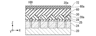
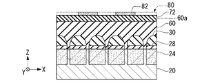
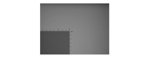
- FIG. 1 It is a side sectional view of the optical structure of one Embodiment which concerns on this invention. It is a side sectional view for demonstrating the manufacturing method of the optical structure shown in FIG. It is a side sectional view for demonstrating the manufacturing method of the optical structure shown in FIG. It is a photograph of the prototype optical structure observed with a metallurgical microscope, and is a photograph of a sample using a low refractive index layer material having a SiO 2 hollow filler content of 91% by mass, observed with a 5x objective lens.
- the optical structure 50 of the embodiment according to the present invention is provided in the distance image sensor 10.
- the distance image sensor 10 includes a substrate 20, a CMOS image sensor 24, a color filter 28, a microlens 30, and an optical structure 50.
- the substrate 20 is, for example, a silicon (Si) substrate.
- the material of the substrate 20 is, for example, Si, but the material is not particularly limited as long as it is provided with pixels such as a CMOS image sensor 24 and a light receiving element and can be made to function electrically.
- the thickness direction of the substrate 20 is defined as the Z direction, and the direction from the inside of the substrate 20 toward the surface 20a in the Z direction is defined as “front”.
- one direction parallel to the surface 20a and orthogonal to the Z direction is defined as the X direction
- a direction parallel to the surface 20a and orthogonal to the X direction and the Z direction is defined as the Y direction.
- the distance image sensor 10 includes a plurality of CMOS image sensors 24.
- the plurality of CMOS image sensors 24 are arranged along each of the X direction and the Y direction.
- the pixel array of the distance image sensor 10 is configured in the direction along the surface 20a of the substrate 20.
- the number of CMOS image sensors 24 provided in the distance image sensor 10 is appropriately set according to the intended use of the distance image sensor 10, and at least a part thereof is exemplified in FIG. 1 and the like.
- Each CMOS image sensor 24 is embedded on the surface 20a side of the substrate 20 in the Z direction.
- the light receiving surface 25 of the CMOS image sensor 24 is exposed from the substrate 20 and is substantially flush with the surface 20a.
- FIG. 1 and the like the illustration of the detailed structure of the CMOS image sensor 24 is omitted.
- the detailed configuration of the CMOS image sensor 24 is the same as that of a known CMOS image sensor.
- the color filter 28 is provided on the light receiving surface 25 of each CMOS image sensor 24 (that is, in front of the Z direction).
- the color filter 28 has a function of transmitting light in a wavelength band of any of red (R), green (G), and blue (B), which are the three primary colors of light.
- the color transmitted by the color filter 28 is appropriately determined for each of the plurality of CMOS image sensors 24 according to the arrangement of the plurality of CMOS image sensors 24 and the like.
- the microlens 30 is provided on the surface 28a of the color filter 28 on each CMOS image sensor 24.
- the microlens 30 is a so-called plano-convex lens having a bottom surface 30b and a lens surface 30a.
- the material of the microlens 30 has a refractive index higher than at least the refractive index of air or the low refractive index layer 60.
- the material of the microlens 30 is a high refractive index material having a refractive index of 1.4 to 1.6 in order to obtain a refractive index difference from the low refractive index layer 60 and enhance the light collecting action of the microlens. Is preferable.
- the curvature and shape of the lens surface 30a are appropriately designed according to the refractive index of the material of the microlens 30 at the visible wavelength and the like. Further, the microlens 30 is formed and arranged so as to focus the light incident in the direction opposite to the Z direction from the front in the Z direction to the CMOS image sensor 24 through the color filter 28 below (that is, behind in the Z direction). ..
- the optical structure 50 is provided in front of the substrate 20 in the Z direction, covers a plurality of color filters 28 and a plurality of microlenses 30, and comprises a low refractive index layer (layer) 60 and a diffraction grating (functional layer) 70. Be prepared.
- the low refractive index layer 60 forms a flat surface 65 for providing a diffraction grating 70 in front of the microlens 30 on the surface 60a in front of the Z direction, and the flat surface 65 in the Z direction, a color filter 28, and a microlens. It is provided to physically fill the space between the 30s and the surface 20a of the substrate 20 that is exposed.
- the maximum thickness of the low refractive index layer 60 (that is, the magnitude in the Z direction between the flat surface 65 and the surface 20a) is set to a predetermined thickness, and is required for light incident on the microlens 30 from the front in the Z direction. It is determined as appropriate according to the optical path length and the like.
- Low of the low refractive index layer 60 means having a refractive index lower than that of the microlens 30 and having a refractive index as close as possible to the refractive index of air. Since the refractive index of the low refractive index layer 60 is close to the refractive index of air, the difference in refractive index between the low refractive index layer 60 and the microlens 30 can be increased. As a result, it is possible to suppress the refraction of the light incident on the diffraction grating 70 in the direction opposite to the Z direction from the front in the Z direction, and to direct the path of the light incident on the diffraction grating 70 in a predetermined direction.
- the refractive index of the low refractive index layer 60 at a visible wavelength is equivalent to 1, which is the refractive index of air.
- the refractive index of the low refractive index layer 60 at a visible wavelength is more preferably 1.25 or more and 1.33 or less, and 1.27 or more 1. It is more preferably 30 or less.
- the effect of the present invention can be obtained when the refractive index of the low refractive index layer 60 at a visible wavelength is 1.25 or more.
- the refractive index of the low refractive index layer 60 is appropriately adjusted in consideration of the type of the low refractive index material described below and the content of the low refractive index material in the low refractive index layer 60.
- the low refractive index layer 60 contains a low refractive index material and a medium.
- Low refractive index materials and media are transparent at visible wavelengths, for example, have a total light transmittance of 90% or more with respect to light at visible wavelengths.
- the low refractive index material contributes to bring the refractive index of the low refractive index layer 60 as close as possible to the refractive index of air.
- the medium intervenes between the particles of the low-refractive index material, adheres the low-refractive index materials to each other, and plays the role of an adhesive and an adhesive for stabilizing the low-refractive index layer 60.
- the content of the low refractive index material in the low refractive index layer 60 is preferably 60% by mass or more and 76% by mass or less, and preferably 70% by mass or more and 76% by mass or less.
- the content of the low refractive index material in the low refractive index layer 60 is less than 60% by mass, the contribution of the low refractive index material to the refractive index of the low refractive index layer 60 weakens, and the refractive index of the low refractive index layer 60 becomes excessive. Therefore, it may not be possible to suppress the refraction of the light incident on the diffraction grid 70 as described above.
- the content of the low refractive index material in the low refractive index layer 60 exceeds 76% by mass, the relative amount of the medium with respect to the low refractive index material in the low refractive index layer 60 is greatly reduced, and the particles of the low refractive index material are interleaved.
- the gap becomes large.
- the material of the diffraction grating is formed in a layer on the low refractive index layer 60 as described later, the material of the diffraction grating permeates into the gaps between the particles of the low refractive index material, and the low refractive index layer 60 is formed. Spots occur.
- the stain may act as a wavefront conversion pattern for the light, the light may be diffused by the stain, and it may be difficult for the microlens 30 to focus the light on the CMOS image sensor 24. That is, when the content of the low refractive index material in the low refractive index layer 60 is outside the range of 60% by mass or more and 76% by mass or less, it is incident on the diffraction grating 70 when the optical structure 50 is applied to the distance image sensor 10. The refraction of light cannot be suppressed. Therefore, or because it is difficult to focus the light on the CMOS image sensor 24, the appearance of the optical structure 50 is poor, and the desired optical characteristics cannot be obtained.
- the low refractive index material preferably contains, for example, silicon dioxide (silica, SiO 2 ) and is an inorganic hollow filler made of an inorganic substance such as SiO 2 . Since the low refractive index material contains SiO 2 , it is inexpensive, and high transparency and physical stability with respect to visible wavelengths can be obtained. Further, since the low refractive index material is an inorganic hollow filler, air regions due to the inorganic hollow filler are scattered inside the low refractive index layer 60, and the refractive index of the entire low refractive index layer 60 approaches the refractive index of air. The increase in the refractive index of the low refractive index layer 60 is suppressed.
- the low refractive index material is a hollow filler of SiO 2
- both the above-mentioned advantages of having SiO 2 and the above-mentioned advantages of having an inorganic hollow filler can be obtained.
- the size of the average inner diameter of the hollow portion with respect to the average particle size of the hollow filler is, for example, about 50%, and has an appropriate strength. From the viewpoint of exerting it, it is 40% or more and 60% or less.
- the diffraction grating 70 is periodically provided on the surface 60a of the low refractive index layer 60 at predetermined intervals in the X direction and the Y direction.
- Light incident on the diffraction grating 70 from the front in the Z direction in the direction opposite to the Z direction is diffracted by the diffraction grating 70 in the vicinity of the flat surface 65 (that is, the diffraction surface), and the wavelength of the light with respect to the normal line along the Z direction. It is diffracted at a diffraction angle determined by the pitch 70d of the diffraction grating 70, and travels in a different direction for each wavelength.
- the size 70g and the pitch 70d of the diffraction grating 70 in each of the X direction and the Y direction are the color filters 28 and the X direction corresponding to the light of each color of RGB among the light diffracted by the diffraction grating 70 as described above. It is appropriately designed to irradiate the microlens 30 and the CMOS image sensor 24 that overlap in the Y direction.
- the diffraction grating 70 has transparency at a visible wavelength, and has a total light transmittance of 90% or more with respect to light having a visible wavelength, for example.
- the material of the diffraction grating 70 is not particularly limited as long as it is transparent to light of visible wavelength as described above and can diffract the incident light in a desired direction for each wavelength.
- a material that can be further patterned is suitable as the material of the diffraction grating 70, for example, a resin material containing an acrylic resin. Can be mentioned.
- the CMOS image sensor 24, the color filter 28, and the microlens 30 are formed by known manufacturing methods for each.
- a method of forming a plurality of CMOS image sensors 24 on a substrate 20 such as a Si substrate a patterning and photolithography method can be used as in the optical structure 50, and reactive ion etching (RIE) can be used. Etc. can be used.
- RIE reactive ion etching
- Etc. can be used.
- a method for forming the color filter 28 for example, a pigment-based color resist is applied on the surface 20a of the substrate 20 and the light receiving surface 25 of the CMOS image sensor 24, and exposed, developed, and developed based on a photolithography method.
- a method of repeating each baking process for three colors of RGB can be mentioned.
- a method of etching and transferring the lens pattern according to the above method to a layer of a high refractive index material underneath can be mentioned.
- a low refractive index material is provided so as to cover the surface 20a of the substrate 20 exposed between the color filter 28 and the microlens 30, and the low refractive index layer 60 is formed. .. After that, the surface 60a on the front side in the Z direction of the low refractive index layer 60 is flattened.
- a method for forming the low refractive index layer 60 in this way for example, a method of applying a low refractive index material to the surface 20a of the substrate 20 and thermosetting it can be mentioned.
- the material 72 of the diffraction grating 70 is applied to the surface 60a of the low refractive index layer 60 with a predetermined thickness.
- the material 72 is a patternable material that can realize the optical characteristics required for the diffraction grating 70 and has photosensitivity, and is a resin material such as an acrylic resin.
- a photomask 80 is placed on the material 72 coated on the surface 60a of the low refractive index layer 60 (that is, forward in the Z direction).
- the photomask 80 has a pattern similar to that of the diffraction grating 70.
- a light-shielding material 82 such as chromium (Cr). Is provided.
- the portion other than the light-shielding material 82 is formed of, for example, quartz (SiO 2 ) or the like, and light (for example, ultraviolet light) at the time of pattern transfer in the photolithography step is transmitted in the Z direction.
- the material 72 is exposed to light from the front in the Z direction of the photomask 80 in the direction opposite to the Z direction, and the pattern of the photomask 80 is transferred to the material 72.
- the material 72 other than the portion overlapping with the light-shielding material 82 in the Z direction is exposed to light.
- a diffraction grating 70 is formed on the surface 60a of the low refractive index layer 60 as shown in FIG. ..
- low refractive index material a material in which a SiO 2 hollow filler (low refractive index material) and a binder (medium) are mixed. (Described as a rate layer material) was prepared.
- the average particle size of the SiO 2 hollow filler was 60 nm.
- the average diameter of the hollow portion of the SiO 2 hollow filler was 40 nm, and the average diameter of the outer portion of SiO 2 in the radial direction was 10 nm.
- the content of the SiO 2 hollow fillers (that is, the mass% ratio in the low refractive index layer material) was 91% by mass, 81% by mass, 76% by mass, 71% by mass,
- the low refractive index layer materials ⁇ 1> to ⁇ 5> were adjusted in the above-mentioned order by varying in 5 types of 66% by mass.
- a Si substrate having a thickness of 725 ⁇ m is prepared as the substrate 20, and a low refractive index layer material is formed on the Si substrate for each of the low refractive index layer materials ⁇ 1> to ⁇ 5> to form the low refractive index layer material.
- a first sample in which the diffraction grating forming layer was formed on the Si substrate and a second sample in which only the diffraction grating forming layer was formed on the Si substrate were prepared. That is, each of the low refractive index layer materials ⁇ 1> to ⁇ 5> and the material of the diffraction grating forming layer were formed on the Si substrate as a so-called solid film.
- a transparent thermosetting resin material containing an acrylic resin as a main component was used as a material constituting the diffraction grating 70.
- FIGS. 4 to 6 show a metallurgical microscope (model number; MX50, manufactured by Olympus Corporation) of the first sample of the low refractive index layer materials ⁇ 1>, ⁇ 3>, and ⁇ 4> along the thickness direction from the diffraction grating forming layer side. It is a photograph observed with an objective lens of 5 times ( ⁇ 5) of. 7 to 9 show that the first samples of the low refractive index layer materials ⁇ 1>, ⁇ 3>, and ⁇ 4> are 20 times larger ( ⁇ 20) than the above-mentioned metallurgical microscope along the thickness direction from the diffraction grating forming layer side. ) Is a photograph observed with an objective lens. As shown in FIGS.
- the amount of penetration and the refractive index of the material of the diffraction grating forming layer in each of the low refractive index layer materials ⁇ 1> to ⁇ 5> were measured.
- the total thickness (A) of the low refractive index layer and the diffraction grating forming layer in the first sample is based on the film thickness measurement by a step meter (model number; P-16, manufactured by KLA-Tencor).
- the thickness (B) of only the low refractive index layer in one sample was measured as the difference (C).
- Table 2 shows the results of measuring the permeation amount and the refractive index of the material of the diffraction grating forming layer for each of the low refractive index layer materials ⁇ 1> to ⁇ 5>.
- the column of "filler content” in Table 1 represents the content of the SiO 2 hollow filler in the low refractive index layer material.
- judgment when the condition that the refractive index is 1.33 or less and the penetration amount is 0.06 ⁇ m or less is satisfied, it is regarded as “ ⁇ ”, and when the above condition is not satisfied, it is regarded as “ ⁇ ”. bottom.
- FIG. 10 shows a photograph observed at ⁇ 100 k using (manufactured by Tencor).
- the variable n in FIG. 10 represents the refractive index of each of the low refractive index layer materials ⁇ 1> to ⁇ 5>.
- the content of the binder (resin, medium) in the layer material increases. Therefore, it is considered that the SiO 2 hollow fillers are in close contact with each other via the binder, and the gap between the SiO 2 hollow fillers, that is, the total volume of the voids in the low refractive index layer is reduced, and as a result, stains do not occur.
- the binder content in the low index layer material is low. Therefore, it is considered that the SiO 2 hollow fillers do not adhere to each other via the binder, the gaps between the SiO 2 hollow fillers widen, and the total volume of the voids in the low refractive index layer increases, resulting in stains.
- the material 72 of the diffraction grating 70 that is, the transparent resin of the diffraction grating forming layer in this experiment. It is presumed that the material) permeates into the void 100 from the surface 60a in the direction opposite to the Z direction as illustrated by the two-point chain line in FIG. 2, and the permeation substantially stops when the material 72 is cured. As a result, it is considered that as the content of the SiO 2 hollow filler in the low refractive index layer material decreases, a stain is generated in the region close to the surface 60a in the Z direction of the low refractive index layer 60.
- the lower the content of the SiO 2 hollow filler in the low refractive index layer material the smaller the total volume of the hollow portion in the low refractive index layer 60, and the lower the refractive index layer.
- the refractive index of 60 becomes high.
- the content of the SiO 2 hollow filler in the low refractive index layer material is less than 60% by mass, the refractive index of the low refractive index layer 60 becomes excessively high, for example, exceeding 1.33.
- the content of the SiO 2 hollow filler in the low refractive index layer material increases, the total volume of the hollow portion in the low refractive index layer 60 increases, and the refractive index of the low refractive index layer 60 decreases.
- the low refractive index layer materials ⁇ 3> to ⁇ 5> that satisfy the conditions that the refractive index of the low refractive index layer 60 is 1.33 or less and the penetration amount is 0.06 ⁇ m or less. Therefore, it was confirmed that the content of the SiO 2 hollow filler in the low refractive index layer material was 66% by mass or more and 76% or less. Further, in consideration of the effect of increasing the refractive index, the content of the SiO 2 hollow filler in the low refractive index layer material is 60% by mass or more and 76% or less, so that the effect of suppressing the increase in the refractive index and the effect of suppressing the generation of stains are achieved. It is thought that both effects are exhibited.
- the optical structure 50 of the present embodiment described above includes a low refractive index layer 60 including a low refractive index material and a medium, and a diffraction grating 70 provided on the surface 60a of the low refractive index layer 60.
- the content of the low refractive index material in the low refractive index layer 60 is 60% by mass or more and 76% by mass or less.
- the content of the low refractive index material in the low refractive index layer 60 is 60% by mass or more, so that the refractive index of the low refractive index layer 60 is as close as possible to the refractive index of air and is a realistic value. Can be set to.
- the content of the low refractive index material in the low refractive index layer 60 is 76% by mass or less, the particles of the low refractive index material are brought into close contact with each other via the medium, and the low refractive index layer 60 is formed. It is possible to prevent the material of the diffraction grid 70 from infiltrating into the low refractive index layer 60 by making the voids almost eliminated.
- the refractive index of the low refractive index layer 60 at the visible wavelength is 1.25 or more and 1.33 or less.
- the refraction of light in the low refractive index layer 60 can be suppressed, and the light incident on the adjacent structures in the Z direction (that is, the thickness direction) can be advanced in a desired direction.
- the distance image sensor 10 provided with the optical structure 50 the refraction of light in the low refractive index layer 60 is suppressed, and the light traveling through the low refractive index layer 60 is passed through a desired color filter 28 by a microlens 30 to obtain a desired value. It can be well focused on the CMOS image sensor 24. As a result, the desired optical characteristics of the distance image sensor 10 can be achieved.
- the low refractive index material of the low refractive index layer 60 contains silicon dioxide (SiO 2 ). According to the optical structure 50 of the present embodiment, it is possible to realize good transparency of the low refractive index layer 60 at a visible wavelength and a refractive index close to that of air to some extent.
- the low refractive index material of the low refractive index layer 60 contains an inorganic hollow filler having transparency at a visible wavelength, for example, a hollow filler of SiO 2 . According to the optical structure 50 of the present embodiment, the hollow portions of the inorganic hollow filler are scattered in the low refractive index layer 60, and the increase in the refractive index of the low refractive index layer 60 can be effectively suppressed.
- the present invention is not limited to a specific embodiment, and includes configuration changes and combinations within a range that does not deviate from the gist of the present invention. Some changes are illustrated below, but not all, and other changes are possible. Two or more of these changes may be combined as appropriate.
- the optical structure 50 is applied to the distance image sensor 10 and is arranged in front of the microlens 30 in the Z direction, but the configuration adjacent to the optical structure 50 in the Z direction is the substrate 20. It is not limited to a laminated structure having a CMOS image sensor 24, a color filter 28, and a microlens 30.
- the optical structure 50 is an arbitrary configuration that requires a low refractive index layer 60 having a refractive index as close as possible to air (that is, a low refractive index) and a diffraction grating 70 provided on the surface 60a of the low refractive index layer 60. Can be applied to elements.
- the present invention is not limited to the above-described embodiment, and can be widely applied to a lens array in which a low refractive index layer containing a hollow filler is formed on a microlens and another layer is formed on the low refractive index layer. Therefore, for example, it can be applied to a lens sheet or the like arranged on an organic EL (OLED).
- OLED organic EL
- the organic EL may be covered with a cover layer such as glass.
- peeling may occur between the microlens and the cover layer due to the unevenness of the lens. Therefore, it is preferable to provide a low refractive index layer between the microlens and the cover layer.
- a cover layer such as an organic EL, a color filter, a lens array (microlens and a low refractive index layer) of the present invention, and glass is laminated in this order. Even in this case, the formation of stains can be suppressed by adopting the configuration of the present invention.
- the functional layer formed on the low refractive index layer is not limited to the above-mentioned diffraction grating, but is the case of any layer formed by using a coating liquid containing a solvent, such as an antiglare layer and an antifouling layer.
- a coating liquid containing a solvent such as an antiglare layer and an antifouling layer.
- the technical idea of the invention can be applied.
- the above-mentioned cover layer is also an aspect of the functional layer.
Landscapes
- Physics & Mathematics (AREA)
- General Physics & Mathematics (AREA)
- Optics & Photonics (AREA)
- Diffracting Gratings Or Hologram Optical Elements (AREA)
- Solid State Image Pick-Up Elements (AREA)
Priority Applications (3)
| Application Number | Priority Date | Filing Date | Title |
|---|---|---|---|
| CN202180068594.8A CN116348791A (zh) | 2020-10-13 | 2021-10-05 | 光学结构 |
| JP2022557387A JPWO2022080186A1 (https=) | 2020-10-13 | 2021-10-05 | |
| US18/299,753 US12535627B2 (en) | 2020-10-13 | 2023-04-13 | Optical assembly |
Applications Claiming Priority (2)
| Application Number | Priority Date | Filing Date | Title |
|---|---|---|---|
| JP2020172704 | 2020-10-13 | ||
| JP2020-172704 | 2020-10-13 |
Related Child Applications (1)
| Application Number | Title | Priority Date | Filing Date |
|---|---|---|---|
| US18/299,753 Continuation US12535627B2 (en) | 2020-10-13 | 2023-04-13 | Optical assembly |
Publications (1)
| Publication Number | Publication Date |
|---|---|
| WO2022080186A1 true WO2022080186A1 (ja) | 2022-04-21 |
Family
ID=81207982
Family Applications (1)
| Application Number | Title | Priority Date | Filing Date |
|---|---|---|---|
| PCT/JP2021/036799 Ceased WO2022080186A1 (ja) | 2020-10-13 | 2021-10-05 | 光学構造 |
Country Status (4)
| Country | Link |
|---|---|
| US (1) | US12535627B2 (https=) |
| JP (1) | JPWO2022080186A1 (https=) |
| CN (1) | CN116348791A (https=) |
| WO (1) | WO2022080186A1 (https=) |
Cited By (1)
| Publication number | Priority date | Publication date | Assignee | Title |
|---|---|---|---|---|
| WO2023218842A1 (ja) * | 2022-05-10 | 2023-11-16 | 凸版印刷株式会社 | マイクロレンズアレイおよび固体撮像素子 |
Citations (3)
| Publication number | Priority date | Publication date | Assignee | Title |
|---|---|---|---|---|
| JP2013038164A (ja) * | 2011-08-05 | 2013-02-21 | Sony Corp | 固体撮像装置、電子機器 |
| JP2014074874A (ja) * | 2011-12-28 | 2014-04-24 | Fujifilm Corp | 光学部材セット及びこれを用いた固体撮像素子 |
| JP2020115515A (ja) * | 2019-01-17 | 2020-07-30 | ソニーセミコンダクタソリューションズ株式会社 | 撮像装置及び電子機器 |
Family Cites Families (7)
| Publication number | Priority date | Publication date | Assignee | Title |
|---|---|---|---|---|
| JP6247534B2 (ja) * | 2010-10-20 | 2017-12-13 | スリーエム イノベイティブ プロパティズ カンパニー | 光学拡散性低屈折率要素 |
| WO2013148407A1 (en) * | 2012-03-30 | 2013-10-03 | 3M Innovative Properties Company | Protective coating for low index material |
| JP5825685B2 (ja) * | 2012-10-11 | 2015-12-02 | 株式会社タムロン | 反射防止膜の製造方法 |
| JP6661286B2 (ja) * | 2014-06-30 | 2020-03-11 | 三星電子株式会社Samsung Electronics Co.,Ltd. | 樹脂膜、光学部材および偏光部材 |
| JP2016206682A (ja) * | 2016-08-10 | 2016-12-08 | 株式会社タムロン | 光学素子 |
| EP3413100B1 (en) * | 2016-09-27 | 2020-11-04 | LG Chem, Ltd. | Antireflection film |
| JP2019195051A (ja) | 2018-05-01 | 2019-11-07 | キヤノン株式会社 | 光電変換装置および機器 |
-
2021
- 2021-10-05 WO PCT/JP2021/036799 patent/WO2022080186A1/ja not_active Ceased
- 2021-10-05 CN CN202180068594.8A patent/CN116348791A/zh active Pending
- 2021-10-05 JP JP2022557387A patent/JPWO2022080186A1/ja active Pending
-
2023
- 2023-04-13 US US18/299,753 patent/US12535627B2/en active Active
Patent Citations (3)
| Publication number | Priority date | Publication date | Assignee | Title |
|---|---|---|---|---|
| JP2013038164A (ja) * | 2011-08-05 | 2013-02-21 | Sony Corp | 固体撮像装置、電子機器 |
| JP2014074874A (ja) * | 2011-12-28 | 2014-04-24 | Fujifilm Corp | 光学部材セット及びこれを用いた固体撮像素子 |
| JP2020115515A (ja) * | 2019-01-17 | 2020-07-30 | ソニーセミコンダクタソリューションズ株式会社 | 撮像装置及び電子機器 |
Cited By (2)
| Publication number | Priority date | Publication date | Assignee | Title |
|---|---|---|---|---|
| WO2023218842A1 (ja) * | 2022-05-10 | 2023-11-16 | 凸版印刷株式会社 | マイクロレンズアレイおよび固体撮像素子 |
| EP4524621A4 (en) * | 2022-05-10 | 2025-09-03 | Toppan Holdings Inc | Microlens array and solid-state imaging element |
Also Published As
| Publication number | Publication date |
|---|---|
| JPWO2022080186A1 (https=) | 2022-04-21 |
| CN116348791A (zh) | 2023-06-27 |
| US20230244013A1 (en) | 2023-08-03 |
| US12535627B2 (en) | 2026-01-27 |
Similar Documents
| Publication | Publication Date | Title |
|---|---|---|
| US7750360B2 (en) | Solid-state image pickup device | |
| CN100365820C (zh) | 固体摄像器件、固体摄像器件的制造方法、摄影机 | |
| CN100511695C (zh) | Cmos图像传感器及其制造方法 | |
| JP2009252978A (ja) | 固体撮像素子およびその製造方法 | |
| CN1997929A (zh) | 透镜阵列及其制作方法 | |
| CN108352390A (zh) | 固态成像器件及其制造方法 | |
| JP5037044B2 (ja) | カラー・イメージ・センサ | |
| CN1893025A (zh) | 用于制造cmos图像传感器的方法 | |
| CN100474603C (zh) | Cmos图像传感器及其制造方法 | |
| US20120170113A1 (en) | Infrared transmission optics formed with anti-reflection pattern, and manufacturing method thereof | |
| WO2022080186A1 (ja) | 光学構造 | |
| CN104517986A (zh) | 固体摄像装置及其制造方法 | |
| US20250015113A1 (en) | Solid-state imaging element and method for manufacturing same | |
| JP6801230B2 (ja) | 固体撮像素子および電子機器 | |
| CN1822378A (zh) | 具有衍射透镜的图像传感器及其制造方法 | |
| WO2009144866A1 (ja) | 固体撮像装置 | |
| WO2023218842A1 (ja) | マイクロレンズアレイおよび固体撮像素子 | |
| JP2010054923A (ja) | カラー撮像デバイスおよびカラー撮像デバイスの製造方法 | |
| CN1992308A (zh) | Cmos图像传感器及其制造方法 | |
| US20090152661A1 (en) | Image sensor and method for manufacturing the same | |
| JP2897472B2 (ja) | 色分解フィルターの製造方法 | |
| JP2023038523A (ja) | レンズアレイおよびその製造方法、並びに固体撮像素子 | |
| JP4483294B2 (ja) | 固体撮像素子及びその製造方法 | |
| JP2009168874A (ja) | カラーフィルタ製造用のフォトマスク | |
| CN103941551A (zh) | 一种曝光用掩模板、曝光设备及显示用基板的制作方法 |
Legal Events
| Date | Code | Title | Description |
|---|---|---|---|
| 121 | Ep: the epo has been informed by wipo that ep was designated in this application |
Ref document number: 21879926 Country of ref document: EP Kind code of ref document: A1 |
|
| ENP | Entry into the national phase |
Ref document number: 2022557387 Country of ref document: JP Kind code of ref document: A |
|
| NENP | Non-entry into the national phase |
Ref country code: DE |
|
| 122 | Ep: pct application non-entry in european phase |
Ref document number: 21879926 Country of ref document: EP Kind code of ref document: A1 |