WO2022080186A1 - 光学構造 - Google Patents
光学構造 Download PDFInfo
- Publication number
- WO2022080186A1 WO2022080186A1 PCT/JP2021/036799 JP2021036799W WO2022080186A1 WO 2022080186 A1 WO2022080186 A1 WO 2022080186A1 JP 2021036799 W JP2021036799 W JP 2021036799W WO 2022080186 A1 WO2022080186 A1 WO 2022080186A1
- Authority
- WO
- WIPO (PCT)
- Prior art keywords
- refractive index
- low refractive
- layer
- index layer
- optical structure
- Prior art date
Links
- 230000003287 optical effect Effects 0.000 title claims abstract description 55
- 239000010410 layer Substances 0.000 claims abstract description 173
- 239000000463 material Substances 0.000 claims abstract description 125
- 239000002346 layers by function Substances 0.000 claims abstract description 9
- 239000000945 filler Substances 0.000 claims description 42
- VYPSYNLAJGMNEJ-UHFFFAOYSA-N Silicium dioxide Chemical compound O=[Si]=O VYPSYNLAJGMNEJ-UHFFFAOYSA-N 0.000 claims description 9
- 239000000377 silicon dioxide Substances 0.000 claims description 4
- 235000012239 silicon dioxide Nutrition 0.000 claims description 3
- 229910004298 SiO 2 Inorganic materials 0.000 description 37
- 239000000758 substrate Substances 0.000 description 23
- 238000000034 method Methods 0.000 description 14
- 239000002245 particle Substances 0.000 description 8
- 239000011230 binding agent Substances 0.000 description 7
- 230000000694 effects Effects 0.000 description 7
- 238000006243 chemical reaction Methods 0.000 description 6
- 239000011347 resin Substances 0.000 description 6
- 229920005989 resin Polymers 0.000 description 6
- 230000035515 penetration Effects 0.000 description 5
- 239000012466 permeate Substances 0.000 description 5
- 238000000206 photolithography Methods 0.000 description 5
- 230000015572 biosynthetic process Effects 0.000 description 4
- 238000004519 manufacturing process Methods 0.000 description 4
- 238000000059 patterning Methods 0.000 description 4
- 239000004925 Acrylic resin Substances 0.000 description 3
- 229920000178 Acrylic resin Polymers 0.000 description 3
- 238000002474 experimental method Methods 0.000 description 3
- 238000005259 measurement Methods 0.000 description 3
- 239000000126 substance Substances 0.000 description 3
- 239000000853 adhesive Substances 0.000 description 2
- 230000001070 adhesive effect Effects 0.000 description 2
- 239000011651 chromium Substances 0.000 description 2
- 239000011248 coating agent Substances 0.000 description 2
- 238000000576 coating method Methods 0.000 description 2
- 239000003086 colorant Substances 0.000 description 2
- 230000007423 decrease Effects 0.000 description 2
- 239000011521 glass Substances 0.000 description 2
- 239000007788 liquid Substances 0.000 description 2
- 238000001020 plasma etching Methods 0.000 description 2
- 239000007787 solid Substances 0.000 description 2
- 229920001187 thermosetting polymer Polymers 0.000 description 2
- 238000002834 transmittance Methods 0.000 description 2
- VYZAMTAEIAYCRO-UHFFFAOYSA-N Chromium Chemical compound [Cr] VYZAMTAEIAYCRO-UHFFFAOYSA-N 0.000 description 1
- 206010034972 Photosensitivity reaction Diseases 0.000 description 1
- XUIMIQQOPSSXEZ-UHFFFAOYSA-N Silicon Chemical compound [Si] XUIMIQQOPSSXEZ-UHFFFAOYSA-N 0.000 description 1
- 230000003373 anti-fouling effect Effects 0.000 description 1
- 238000013459 approach Methods 0.000 description 1
- 229910052804 chromium Inorganic materials 0.000 description 1
- 230000000295 complement effect Effects 0.000 description 1
- 230000007547 defect Effects 0.000 description 1
- 238000011161 development Methods 0.000 description 1
- 238000005530 etching Methods 0.000 description 1
- 238000009434 installation Methods 0.000 description 1
- 230000001678 irradiating effect Effects 0.000 description 1
- 238000002844 melting Methods 0.000 description 1
- 230000008018 melting Effects 0.000 description 1
- 229920002120 photoresistant polymer Polymers 0.000 description 1
- 230000036211 photosensitivity Effects 0.000 description 1
- 239000000049 pigment Substances 0.000 description 1
- 238000012545 processing Methods 0.000 description 1
- 239000004065 semiconductor Substances 0.000 description 1
- 229910052710 silicon Inorganic materials 0.000 description 1
- 239000010703 silicon Substances 0.000 description 1
- 239000002904 solvent Substances 0.000 description 1
- 230000000087 stabilizing effect Effects 0.000 description 1
- 238000012546 transfer Methods 0.000 description 1
- 239000011800 void material Substances 0.000 description 1
Images


Classifications
-
- G—PHYSICS
- G02—OPTICS
- G02B—OPTICAL ELEMENTS, SYSTEMS OR APPARATUS
- G02B5/00—Optical elements other than lenses
- G02B5/18—Diffraction gratings
- G02B5/1866—Transmission gratings characterised by their structure, e.g. step profile, contours of substrate or grooves, pitch variations, materials
-
- G—PHYSICS
- G02—OPTICS
- G02B—OPTICAL ELEMENTS, SYSTEMS OR APPARATUS
- G02B1/00—Optical elements characterised by the material of which they are made; Optical coatings for optical elements
- G02B1/10—Optical coatings produced by application to, or surface treatment of, optical elements
-
- G—PHYSICS
- G02—OPTICS
- G02B—OPTICAL ELEMENTS, SYSTEMS OR APPARATUS
- G02B5/00—Optical elements other than lenses
- G02B5/18—Diffraction gratings
-
- G—PHYSICS
- G02—OPTICS
- G02B—OPTICAL ELEMENTS, SYSTEMS OR APPARATUS
- G02B5/00—Optical elements other than lenses
- G02B5/18—Diffraction gratings
- G02B5/1814—Diffraction gratings structurally combined with one or more further optical elements, e.g. lenses, mirrors, prisms or other diffraction gratings
-
- G—PHYSICS
- G02—OPTICS
- G02B—OPTICAL ELEMENTS, SYSTEMS OR APPARATUS
- G02B5/00—Optical elements other than lenses
- G02B5/20—Filters
-
- G—PHYSICS
- G02—OPTICS
- G02B—OPTICAL ELEMENTS, SYSTEMS OR APPARATUS
- G02B5/00—Optical elements other than lenses
- G02B5/18—Diffraction gratings
- G02B2005/1804—Transmission gratings
-
- G—PHYSICS
- G02—OPTICS
- G02B—OPTICAL ELEMENTS, SYSTEMS OR APPARATUS
- G02B5/00—Optical elements other than lenses
- G02B5/20—Filters
- G02B5/208—Filters for use with infrared or ultraviolet radiation, e.g. for separating visible light from infrared and/or ultraviolet radiation
Definitions
- the present invention relates to an optical structure.
- This application claims priority based on Japanese Patent Application No. 2020-172704 filed in Japan on October 13, 2020, the contents of which are incorporated herein by reference.
- the distance image sensor detects the flight time (Time of Structure: TOF) from irradiating an object with an optical signal such as infrared rays to receiving reflected light, and distance information to the object based on the TOF.
- TOF type sensor that acquires the distance information to the object by triangular measurement using two cameras
- Structured Light type sensor that uses a projector instead of the above-mentioned camera And so on.
- the distance image sensor is also applied to image authentication systems such as mobile phones. In order to incorporate it into a portable and thin mobile phone, a cheaper and smaller distance image sensor is required.
- a photoelectric conversion unit, a microlens provided on the photoelectric conversion unit, a transparent plate covering the microlens, and a functional film provided between the microlens and the translucent plate A device having a laminated structure with a film) is disclosed.
- the refractive index of the functional film is 1.05 to 1.15
- the functional film contains particles composed of a solid substance such as a resin and a binder for binding the particles.
- CMOS Complementary Metal-Oxide-Semiconductor
- a diffraction grating is used. That is, referring to the structure of the apparatus of Patent Document 1 described above, a CMOS image sensor is provided in the photoelectric conversion unit, and a diffraction grating is formed on the upper surface of the functional layer. In the optical structure formed in this way, the distance information to the object can be acquired by performing image processing on the light demultiplexed for each wavelength by the diffraction grating.
- a flattening layer (a layer corresponding to the above-mentioned functional layer) is provided.
- the flattening layer has a predetermined thickness in order to secure an optical path in the thickness direction of the microlens.
- a diffraction grating material is first provided in layers on the upper surface of the flattening layer, and then a part of the material remains periodically along the surface by patterning or the like. A diffraction grating is formed.
- a low refractive index material having a refractive index close to that of air is used for the flattening layer.
- the material of the diffraction grating permeates between the low refractive index materials of the flattening layer, so that the material is viewed in a plan view along the thickness direction of the flattening layer. Spotted "stains" may occur. When the stains are generated in this way, the appearance is poor and the stains act on the light as a wavefront conversion pattern other than the diffraction grating, so that the desired three-dimensional sensing function cannot be obtained in the optical structure.
- the present invention has been made in view of the above circumstances, and the material of the diffraction grating formed on the surface of the flattening layer is flattened by suppressing an increase in the refractive index and poor appearance of the flattening layer portion (layer).
- an optical structure capable of preventing the formation of stains due to permeation into a layer.
- the optical structure according to the present invention includes a layer containing a low refractive index material and a medium, and a functional layer provided on the surface of the layer, and the content of the low refractive index material in the layer is 60% by mass. It is 76% by mass or less.
- the increase in the refractive index and the appearance defect of the flattening layer portion (layer) in the optical structure are suppressed, and the material of the diffraction grating formed on the surface of the flattening layer (layer) permeates into the flattening layer. It is possible to prevent the formation of stains.
- FIG. 1 It is a side sectional view of the optical structure of one Embodiment which concerns on this invention. It is a side sectional view for demonstrating the manufacturing method of the optical structure shown in FIG. It is a side sectional view for demonstrating the manufacturing method of the optical structure shown in FIG. It is a photograph of the prototype optical structure observed with a metallurgical microscope, and is a photograph of a sample using a low refractive index layer material having a SiO 2 hollow filler content of 91% by mass, observed with a 5x objective lens.
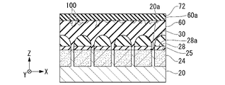
- the optical structure 50 of the embodiment according to the present invention is provided in the distance image sensor 10.
- the distance image sensor 10 includes a substrate 20, a CMOS image sensor 24, a color filter 28, a microlens 30, and an optical structure 50.
- the substrate 20 is, for example, a silicon (Si) substrate.
- the material of the substrate 20 is, for example, Si, but the material is not particularly limited as long as it is provided with pixels such as a CMOS image sensor 24 and a light receiving element and can be made to function electrically.
- the thickness direction of the substrate 20 is defined as the Z direction, and the direction from the inside of the substrate 20 toward the surface 20a in the Z direction is defined as “front”.
- one direction parallel to the surface 20a and orthogonal to the Z direction is defined as the X direction
- a direction parallel to the surface 20a and orthogonal to the X direction and the Z direction is defined as the Y direction.
- the distance image sensor 10 includes a plurality of CMOS image sensors 24.
- the plurality of CMOS image sensors 24 are arranged along each of the X direction and the Y direction.
- the pixel array of the distance image sensor 10 is configured in the direction along the surface 20a of the substrate 20.
- the number of CMOS image sensors 24 provided in the distance image sensor 10 is appropriately set according to the intended use of the distance image sensor 10, and at least a part thereof is exemplified in FIG. 1 and the like.
- Each CMOS image sensor 24 is embedded on the surface 20a side of the substrate 20 in the Z direction.
- the light receiving surface 25 of the CMOS image sensor 24 is exposed from the substrate 20 and is substantially flush with the surface 20a.
- FIG. 1 and the like the illustration of the detailed structure of the CMOS image sensor 24 is omitted.
- the detailed configuration of the CMOS image sensor 24 is the same as that of a known CMOS image sensor.
- the color filter 28 is provided on the light receiving surface 25 of each CMOS image sensor 24 (that is, in front of the Z direction).
- the color filter 28 has a function of transmitting light in a wavelength band of any of red (R), green (G), and blue (B), which are the three primary colors of light.
- the color transmitted by the color filter 28 is appropriately determined for each of the plurality of CMOS image sensors 24 according to the arrangement of the plurality of CMOS image sensors 24 and the like.
- the microlens 30 is provided on the surface 28a of the color filter 28 on each CMOS image sensor 24.
- the microlens 30 is a so-called plano-convex lens having a bottom surface 30b and a lens surface 30a.
- the material of the microlens 30 has a refractive index higher than at least the refractive index of air or the low refractive index layer 60.
- the material of the microlens 30 is a high refractive index material having a refractive index of 1.4 to 1.6 in order to obtain a refractive index difference from the low refractive index layer 60 and enhance the light collecting action of the microlens. Is preferable.
- the curvature and shape of the lens surface 30a are appropriately designed according to the refractive index of the material of the microlens 30 at the visible wavelength and the like. Further, the microlens 30 is formed and arranged so as to focus the light incident in the direction opposite to the Z direction from the front in the Z direction to the CMOS image sensor 24 through the color filter 28 below (that is, behind in the Z direction). ..
- the optical structure 50 is provided in front of the substrate 20 in the Z direction, covers a plurality of color filters 28 and a plurality of microlenses 30, and comprises a low refractive index layer (layer) 60 and a diffraction grating (functional layer) 70. Be prepared.
- the low refractive index layer 60 forms a flat surface 65 for providing a diffraction grating 70 in front of the microlens 30 on the surface 60a in front of the Z direction, and the flat surface 65 in the Z direction, a color filter 28, and a microlens. It is provided to physically fill the space between the 30s and the surface 20a of the substrate 20 that is exposed.
- the maximum thickness of the low refractive index layer 60 (that is, the magnitude in the Z direction between the flat surface 65 and the surface 20a) is set to a predetermined thickness, and is required for light incident on the microlens 30 from the front in the Z direction. It is determined as appropriate according to the optical path length and the like.
- Low of the low refractive index layer 60 means having a refractive index lower than that of the microlens 30 and having a refractive index as close as possible to the refractive index of air. Since the refractive index of the low refractive index layer 60 is close to the refractive index of air, the difference in refractive index between the low refractive index layer 60 and the microlens 30 can be increased. As a result, it is possible to suppress the refraction of the light incident on the diffraction grating 70 in the direction opposite to the Z direction from the front in the Z direction, and to direct the path of the light incident on the diffraction grating 70 in a predetermined direction.
- the refractive index of the low refractive index layer 60 at a visible wavelength is equivalent to 1, which is the refractive index of air.
- the refractive index of the low refractive index layer 60 at a visible wavelength is more preferably 1.25 or more and 1.33 or less, and 1.27 or more 1. It is more preferably 30 or less.
- the effect of the present invention can be obtained when the refractive index of the low refractive index layer 60 at a visible wavelength is 1.25 or more.
- the refractive index of the low refractive index layer 60 is appropriately adjusted in consideration of the type of the low refractive index material described below and the content of the low refractive index material in the low refractive index layer 60.
- the low refractive index layer 60 contains a low refractive index material and a medium.
- Low refractive index materials and media are transparent at visible wavelengths, for example, have a total light transmittance of 90% or more with respect to light at visible wavelengths.
- the low refractive index material contributes to bring the refractive index of the low refractive index layer 60 as close as possible to the refractive index of air.
- the medium intervenes between the particles of the low-refractive index material, adheres the low-refractive index materials to each other, and plays the role of an adhesive and an adhesive for stabilizing the low-refractive index layer 60.
- the content of the low refractive index material in the low refractive index layer 60 is preferably 60% by mass or more and 76% by mass or less, and preferably 70% by mass or more and 76% by mass or less.
- the content of the low refractive index material in the low refractive index layer 60 is less than 60% by mass, the contribution of the low refractive index material to the refractive index of the low refractive index layer 60 weakens, and the refractive index of the low refractive index layer 60 becomes excessive. Therefore, it may not be possible to suppress the refraction of the light incident on the diffraction grid 70 as described above.
- the content of the low refractive index material in the low refractive index layer 60 exceeds 76% by mass, the relative amount of the medium with respect to the low refractive index material in the low refractive index layer 60 is greatly reduced, and the particles of the low refractive index material are interleaved.
- the gap becomes large.
- the material of the diffraction grating is formed in a layer on the low refractive index layer 60 as described later, the material of the diffraction grating permeates into the gaps between the particles of the low refractive index material, and the low refractive index layer 60 is formed. Spots occur.
- the stain may act as a wavefront conversion pattern for the light, the light may be diffused by the stain, and it may be difficult for the microlens 30 to focus the light on the CMOS image sensor 24. That is, when the content of the low refractive index material in the low refractive index layer 60 is outside the range of 60% by mass or more and 76% by mass or less, it is incident on the diffraction grating 70 when the optical structure 50 is applied to the distance image sensor 10. The refraction of light cannot be suppressed. Therefore, or because it is difficult to focus the light on the CMOS image sensor 24, the appearance of the optical structure 50 is poor, and the desired optical characteristics cannot be obtained.
- the low refractive index material preferably contains, for example, silicon dioxide (silica, SiO 2 ) and is an inorganic hollow filler made of an inorganic substance such as SiO 2 . Since the low refractive index material contains SiO 2 , it is inexpensive, and high transparency and physical stability with respect to visible wavelengths can be obtained. Further, since the low refractive index material is an inorganic hollow filler, air regions due to the inorganic hollow filler are scattered inside the low refractive index layer 60, and the refractive index of the entire low refractive index layer 60 approaches the refractive index of air. The increase in the refractive index of the low refractive index layer 60 is suppressed.
- the low refractive index material is a hollow filler of SiO 2
- both the above-mentioned advantages of having SiO 2 and the above-mentioned advantages of having an inorganic hollow filler can be obtained.
- the size of the average inner diameter of the hollow portion with respect to the average particle size of the hollow filler is, for example, about 50%, and has an appropriate strength. From the viewpoint of exerting it, it is 40% or more and 60% or less.
- the diffraction grating 70 is periodically provided on the surface 60a of the low refractive index layer 60 at predetermined intervals in the X direction and the Y direction.
- Light incident on the diffraction grating 70 from the front in the Z direction in the direction opposite to the Z direction is diffracted by the diffraction grating 70 in the vicinity of the flat surface 65 (that is, the diffraction surface), and the wavelength of the light with respect to the normal line along the Z direction. It is diffracted at a diffraction angle determined by the pitch 70d of the diffraction grating 70, and travels in a different direction for each wavelength.
- the size 70g and the pitch 70d of the diffraction grating 70 in each of the X direction and the Y direction are the color filters 28 and the X direction corresponding to the light of each color of RGB among the light diffracted by the diffraction grating 70 as described above. It is appropriately designed to irradiate the microlens 30 and the CMOS image sensor 24 that overlap in the Y direction.
- the diffraction grating 70 has transparency at a visible wavelength, and has a total light transmittance of 90% or more with respect to light having a visible wavelength, for example.
- the material of the diffraction grating 70 is not particularly limited as long as it is transparent to light of visible wavelength as described above and can diffract the incident light in a desired direction for each wavelength.
- a material that can be further patterned is suitable as the material of the diffraction grating 70, for example, a resin material containing an acrylic resin. Can be mentioned.
- the CMOS image sensor 24, the color filter 28, and the microlens 30 are formed by known manufacturing methods for each.
- a method of forming a plurality of CMOS image sensors 24 on a substrate 20 such as a Si substrate a patterning and photolithography method can be used as in the optical structure 50, and reactive ion etching (RIE) can be used. Etc. can be used.
- RIE reactive ion etching
- Etc. can be used.
- a method for forming the color filter 28 for example, a pigment-based color resist is applied on the surface 20a of the substrate 20 and the light receiving surface 25 of the CMOS image sensor 24, and exposed, developed, and developed based on a photolithography method.
- a method of repeating each baking process for three colors of RGB can be mentioned.
- a method of etching and transferring the lens pattern according to the above method to a layer of a high refractive index material underneath can be mentioned.
- a low refractive index material is provided so as to cover the surface 20a of the substrate 20 exposed between the color filter 28 and the microlens 30, and the low refractive index layer 60 is formed. .. After that, the surface 60a on the front side in the Z direction of the low refractive index layer 60 is flattened.
- a method for forming the low refractive index layer 60 in this way for example, a method of applying a low refractive index material to the surface 20a of the substrate 20 and thermosetting it can be mentioned.
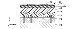
- the material 72 of the diffraction grating 70 is applied to the surface 60a of the low refractive index layer 60 with a predetermined thickness.
- the material 72 is a patternable material that can realize the optical characteristics required for the diffraction grating 70 and has photosensitivity, and is a resin material such as an acrylic resin.
- a photomask 80 is placed on the material 72 coated on the surface 60a of the low refractive index layer 60 (that is, forward in the Z direction).
- the photomask 80 has a pattern similar to that of the diffraction grating 70.
- a light-shielding material 82 such as chromium (Cr). Is provided.
- the portion other than the light-shielding material 82 is formed of, for example, quartz (SiO 2 ) or the like, and light (for example, ultraviolet light) at the time of pattern transfer in the photolithography step is transmitted in the Z direction.
- the material 72 is exposed to light from the front in the Z direction of the photomask 80 in the direction opposite to the Z direction, and the pattern of the photomask 80 is transferred to the material 72.
- the material 72 other than the portion overlapping with the light-shielding material 82 in the Z direction is exposed to light.
- a diffraction grating 70 is formed on the surface 60a of the low refractive index layer 60 as shown in FIG. ..
- low refractive index material a material in which a SiO 2 hollow filler (low refractive index material) and a binder (medium) are mixed. (Described as a rate layer material) was prepared.
- the average particle size of the SiO 2 hollow filler was 60 nm.
- the average diameter of the hollow portion of the SiO 2 hollow filler was 40 nm, and the average diameter of the outer portion of SiO 2 in the radial direction was 10 nm.
- the content of the SiO 2 hollow fillers (that is, the mass% ratio in the low refractive index layer material) was 91% by mass, 81% by mass, 76% by mass, 71% by mass,
- the low refractive index layer materials ⁇ 1> to ⁇ 5> were adjusted in the above-mentioned order by varying in 5 types of 66% by mass.
- a Si substrate having a thickness of 725 ⁇ m is prepared as the substrate 20, and a low refractive index layer material is formed on the Si substrate for each of the low refractive index layer materials ⁇ 1> to ⁇ 5> to form the low refractive index layer material.
- a first sample in which the diffraction grating forming layer was formed on the Si substrate and a second sample in which only the diffraction grating forming layer was formed on the Si substrate were prepared. That is, each of the low refractive index layer materials ⁇ 1> to ⁇ 5> and the material of the diffraction grating forming layer were formed on the Si substrate as a so-called solid film.
- a transparent thermosetting resin material containing an acrylic resin as a main component was used as a material constituting the diffraction grating 70.
- FIGS. 4 to 6 show a metallurgical microscope (model number; MX50, manufactured by Olympus Corporation) of the first sample of the low refractive index layer materials ⁇ 1>, ⁇ 3>, and ⁇ 4> along the thickness direction from the diffraction grating forming layer side. It is a photograph observed with an objective lens of 5 times ( ⁇ 5) of. 7 to 9 show that the first samples of the low refractive index layer materials ⁇ 1>, ⁇ 3>, and ⁇ 4> are 20 times larger ( ⁇ 20) than the above-mentioned metallurgical microscope along the thickness direction from the diffraction grating forming layer side. ) Is a photograph observed with an objective lens. As shown in FIGS.
- the amount of penetration and the refractive index of the material of the diffraction grating forming layer in each of the low refractive index layer materials ⁇ 1> to ⁇ 5> were measured.
- the total thickness (A) of the low refractive index layer and the diffraction grating forming layer in the first sample is based on the film thickness measurement by a step meter (model number; P-16, manufactured by KLA-Tencor).
- the thickness (B) of only the low refractive index layer in one sample was measured as the difference (C).
- Table 2 shows the results of measuring the permeation amount and the refractive index of the material of the diffraction grating forming layer for each of the low refractive index layer materials ⁇ 1> to ⁇ 5>.
- the column of "filler content” in Table 1 represents the content of the SiO 2 hollow filler in the low refractive index layer material.
- judgment when the condition that the refractive index is 1.33 or less and the penetration amount is 0.06 ⁇ m or less is satisfied, it is regarded as “ ⁇ ”, and when the above condition is not satisfied, it is regarded as “ ⁇ ”. bottom.
- FIG. 10 shows a photograph observed at ⁇ 100 k using (manufactured by Tencor).
- the variable n in FIG. 10 represents the refractive index of each of the low refractive index layer materials ⁇ 1> to ⁇ 5>.
- the content of the binder (resin, medium) in the layer material increases. Therefore, it is considered that the SiO 2 hollow fillers are in close contact with each other via the binder, and the gap between the SiO 2 hollow fillers, that is, the total volume of the voids in the low refractive index layer is reduced, and as a result, stains do not occur.
- the binder content in the low index layer material is low. Therefore, it is considered that the SiO 2 hollow fillers do not adhere to each other via the binder, the gaps between the SiO 2 hollow fillers widen, and the total volume of the voids in the low refractive index layer increases, resulting in stains.
- the material 72 of the diffraction grating 70 that is, the transparent resin of the diffraction grating forming layer in this experiment. It is presumed that the material) permeates into the void 100 from the surface 60a in the direction opposite to the Z direction as illustrated by the two-point chain line in FIG. 2, and the permeation substantially stops when the material 72 is cured. As a result, it is considered that as the content of the SiO 2 hollow filler in the low refractive index layer material decreases, a stain is generated in the region close to the surface 60a in the Z direction of the low refractive index layer 60.
- the lower the content of the SiO 2 hollow filler in the low refractive index layer material the smaller the total volume of the hollow portion in the low refractive index layer 60, and the lower the refractive index layer.
- the refractive index of 60 becomes high.
- the content of the SiO 2 hollow filler in the low refractive index layer material is less than 60% by mass, the refractive index of the low refractive index layer 60 becomes excessively high, for example, exceeding 1.33.
- the content of the SiO 2 hollow filler in the low refractive index layer material increases, the total volume of the hollow portion in the low refractive index layer 60 increases, and the refractive index of the low refractive index layer 60 decreases.
- the low refractive index layer materials ⁇ 3> to ⁇ 5> that satisfy the conditions that the refractive index of the low refractive index layer 60 is 1.33 or less and the penetration amount is 0.06 ⁇ m or less. Therefore, it was confirmed that the content of the SiO 2 hollow filler in the low refractive index layer material was 66% by mass or more and 76% or less. Further, in consideration of the effect of increasing the refractive index, the content of the SiO 2 hollow filler in the low refractive index layer material is 60% by mass or more and 76% or less, so that the effect of suppressing the increase in the refractive index and the effect of suppressing the generation of stains are achieved. It is thought that both effects are exhibited.
- the optical structure 50 of the present embodiment described above includes a low refractive index layer 60 including a low refractive index material and a medium, and a diffraction grating 70 provided on the surface 60a of the low refractive index layer 60.
- the content of the low refractive index material in the low refractive index layer 60 is 60% by mass or more and 76% by mass or less.
- the content of the low refractive index material in the low refractive index layer 60 is 60% by mass or more, so that the refractive index of the low refractive index layer 60 is as close as possible to the refractive index of air and is a realistic value. Can be set to.
- the content of the low refractive index material in the low refractive index layer 60 is 76% by mass or less, the particles of the low refractive index material are brought into close contact with each other via the medium, and the low refractive index layer 60 is formed. It is possible to prevent the material of the diffraction grid 70 from infiltrating into the low refractive index layer 60 by making the voids almost eliminated.
- the refractive index of the low refractive index layer 60 at the visible wavelength is 1.25 or more and 1.33 or less.
- the refraction of light in the low refractive index layer 60 can be suppressed, and the light incident on the adjacent structures in the Z direction (that is, the thickness direction) can be advanced in a desired direction.
- the distance image sensor 10 provided with the optical structure 50 the refraction of light in the low refractive index layer 60 is suppressed, and the light traveling through the low refractive index layer 60 is passed through a desired color filter 28 by a microlens 30 to obtain a desired value. It can be well focused on the CMOS image sensor 24. As a result, the desired optical characteristics of the distance image sensor 10 can be achieved.
- the low refractive index material of the low refractive index layer 60 contains silicon dioxide (SiO 2 ). According to the optical structure 50 of the present embodiment, it is possible to realize good transparency of the low refractive index layer 60 at a visible wavelength and a refractive index close to that of air to some extent.
- the low refractive index material of the low refractive index layer 60 contains an inorganic hollow filler having transparency at a visible wavelength, for example, a hollow filler of SiO 2 . According to the optical structure 50 of the present embodiment, the hollow portions of the inorganic hollow filler are scattered in the low refractive index layer 60, and the increase in the refractive index of the low refractive index layer 60 can be effectively suppressed.
- the present invention is not limited to a specific embodiment, and includes configuration changes and combinations within a range that does not deviate from the gist of the present invention. Some changes are illustrated below, but not all, and other changes are possible. Two or more of these changes may be combined as appropriate.
- the optical structure 50 is applied to the distance image sensor 10 and is arranged in front of the microlens 30 in the Z direction, but the configuration adjacent to the optical structure 50 in the Z direction is the substrate 20. It is not limited to a laminated structure having a CMOS image sensor 24, a color filter 28, and a microlens 30.
- the optical structure 50 is an arbitrary configuration that requires a low refractive index layer 60 having a refractive index as close as possible to air (that is, a low refractive index) and a diffraction grating 70 provided on the surface 60a of the low refractive index layer 60. Can be applied to elements.
- the present invention is not limited to the above-described embodiment, and can be widely applied to a lens array in which a low refractive index layer containing a hollow filler is formed on a microlens and another layer is formed on the low refractive index layer. Therefore, for example, it can be applied to a lens sheet or the like arranged on an organic EL (OLED).
- OLED organic EL
- the organic EL may be covered with a cover layer such as glass.
- peeling may occur between the microlens and the cover layer due to the unevenness of the lens. Therefore, it is preferable to provide a low refractive index layer between the microlens and the cover layer.
- a cover layer such as an organic EL, a color filter, a lens array (microlens and a low refractive index layer) of the present invention, and glass is laminated in this order. Even in this case, the formation of stains can be suppressed by adopting the configuration of the present invention.
- the functional layer formed on the low refractive index layer is not limited to the above-mentioned diffraction grating, but is the case of any layer formed by using a coating liquid containing a solvent, such as an antiglare layer and an antifouling layer.
- a coating liquid containing a solvent such as an antiglare layer and an antifouling layer.
- the technical idea of the invention can be applied.
- the above-mentioned cover layer is also an aspect of the functional layer.
Landscapes
- Physics & Mathematics (AREA)
- General Physics & Mathematics (AREA)
- Optics & Photonics (AREA)
- Diffracting Gratings Or Hologram Optical Elements (AREA)
- Solid State Image Pick-Up Elements (AREA)
Abstract
光学構造は、低屈折率材料と媒質とを含む層と、層の表面に設けられた機能層と、を備え、層における低屈折率材料の含有量は60質量%以上76質量%以下である。
Description
本発明は、光学構造に関する。
本願は、2020年10月13日に日本に出願された特願2020-172704号に基づき優先権を主張し、その内容をここに援用する。
本願は、2020年10月13日に日本に出願された特願2020-172704号に基づき優先権を主張し、その内容をここに援用する。
近年、対象物までの距離を情報として含む画像を撮像する距離画像センサの開発が進められている。距離画像センサには、例えば対象物に赤外線等の光信号を照射してから反射光を受光するまでの飛行時間(Time of Flight:TOF)を検出してTOFに基づいて対象物までの距離情報を取得するTOF式センサや、2台のカメラを用いた三角測量によって対象物までの距離情報を取得するStereo Vision方式センサ(又はステレオ視)、前述のカメラの代わりにプロジェクタを用いるStructured Light方式センサ等がある。前述の各方式のセンサでは、筐体や設置スペースの縮小が難しく、消費電力が大きい。
距離画像センサは、携帯電話等の画像認証システムにも適用されている。持ち運び可能で薄型の携帯電話に組み込むにあたり、より安価で小型の距離画像センサが求められる。例えば、特許文献1には、光電変換部と、光電変換部の上に設けられたマイクロレンズと、マイクロレンズを覆う透明板と、マイクロレンズと透光板との間に設けられた機能膜(膜)とを有する積層構造を備えた装置が開示されている。機能膜の屈折率は1.05~1.15であり、機能膜は例えば樹脂等の固体物質で構成された粒子及び粒子を結合するバインダを含有する。
安価で小型な距離画像センサとして、CMOS(Complementary Metal-Oxide-Semiconductor)イメージセンサを用いた3次元センシングデバイスが開発されている。CMOSイメージセンサによって撮像される2次元画像を3次元画像に変換するためには、例えば回折格子を用いる。即ち、上述の特許文献1の装置の構造を参照すると、光電変換部にCMOSイメージセンサを設け、機能層の上面に回折格子を形成する。このように形成された光学構造では、回折格子によって波長毎に分波された光を画像処理することによって、対象物までの距離情報を取得することができる。
上述の光学構造のように、CMOSイメージセンサ等の受光素子を光電変換部の基材の表面に埋設し、基材の表面上にRGBのカラーフィルタやマイクロレンズを形成した場合、マイクロレンズを覆う平坦化層(上述の機能層に相当する層)が設けられる。平坦化層は、マイクロレンズの厚み方向で光路を確保するために、所定の厚みを有する。3次元センシングを可能にする光学構造として、平坦化層の上面には、先ず回折格子の材料が層状に設けられ、続いてパターニング等によって材料の一部が表面に沿う方向で周期的に残り、回折格子が形成される。回折格子を通過した光が所定外の方向に屈折することを防ぐために、平坦化層には、空気に近い屈折率を有する低屈折率材料が用いられる。しかしながら、平坦化層の表面上に回折格子を形成する際に、平坦化層の低屈折率材料間に回折格子の材料が染み込むことによって、平坦化層の厚み方向に沿って平面視したときに斑点状の“シミ”が発生する場合がある。このようにシミが発生すると、外観不良が発生すると共に、光に対してシミが回折格子以外の波面変換パターンとして作用し、光学構造において所望の3次元センシング機能を得られない。
本発明は、上述の事情を鑑みてなされたものであって、平坦化層部分(層)の屈折率の上昇及び外観不良を抑え、平坦化層の表面に形成する回折格子の材料が平坦化層に染み込むことによるシミの形成を防止可能な光学構造を提供する。
本発明に係る光学構造は、低屈折率材料と媒質とを含む層と、前記層の表面に設けられた機能層と、を備え、前記層における前記低屈折率材料の含有量は60質量%以上76質量%以下である。
本発明によれば、光学構造における平坦化層部分(層)の屈折率の上昇及び外観不良を抑え、平坦化層(層)の表面に形成する回折格子の材料が平坦化層に染み込むことによるシミの形成を防止することができる。
以下、本発明に係る実施形態について、図面を参照して説明する。
図1に示すように、本発明に係る一実施形態の光学構造50は、距離画像センサ10に設けられている。距離画像センサ10は、基板20と、CMOSイメージセンサ24と、カラーフィルタ28と、マイクロレンズ30と、光学構造50と、を備える。
基板20は、例えばシリコン(Si)基板である。基板20の材料は、例えばSiであるが、CMOSイメージセンサ24等の画素や受光素子を備えてこれらを電気的に機能させることが可能な材料であれば特に限定されない。以下、基板20の厚み方向をZ方向とし、基板20の内部からZ方向で表面20aに向かう方向を「前」とする。また、表面20aに平行且つZ方向に直交する一方向をX方向とし、表面20aに平行で、且つX方向及びZ方向に直交する方向をY方向とする。
距離画像センサ10は、複数のCMOSイメージセンサ24を備える。複数のCMOSイメージセンサ24は、X方向及びY方向の各々に沿って配列されている。このように複数のCMOSイメージセンサ24が設けられることによって、基板20の表面20aに沿った方向に距離画像センサ10の画素アレイが構成されている。距離画像センサ10に設けられるCMOSイメージセンサ24の数は、距離画像センサ10の使用用途等に応じて適宜設定され、図1等には少なくとも一部が例示されている。
各々のCMOSイメージセンサ24は、Z方向で基板20の表面20a側に埋設されている。CMOSイメージセンサ24の受光面25は、基板20から露出し、表面20aと略面一である。なお、図1等では、CMOSイメージセンサ24の詳細構造の図示は省略されている。CMOSイメージセンサ24の詳細構成は、公知のCMOSイメージセンサと同様である。
カラーフィルタ28は、各々のCMOSイメージセンサ24の受光面25の上(即ち、Z方向前方)に設けられている。カラーフィルタ28は光の3原色である赤(R)・緑(G)・青(B)の何れかの色の波長帯の光を透過させる機能を有する。カラーフィルタ28が透過する色は、複数のCMOSイメージセンサ24の配置等に応じて、複数のCMOSイメージセンサ24毎に適宜決められている。
マイクロレンズ30は、各々のCMOSイメージセンサ24上のカラーフィルタ28の表面28aに設けられている。マイクロレンズ30は、底面30bとレンズ面30aとを有する所謂平凸レンズである。マイクロレンズ30の材料は、少なくとも空気や低屈折率層60の屈折率よりも高い屈折率を有する。特に、低屈折率層60との屈折率差を得てマイクロレンズの集光作用を高めるため、マイクロレンズ30の材料は、1.4~1.6の屈折率を有する高屈折率材料であることが好ましい。レンズ面30aの曲率や形状は、マイクロレンズ30の材料の可視波長における屈折率等に応じて適宜設計されている。また、マイクロレンズ30は、Z方向前方からZ方向とは逆向きに入射する光を下(即ち、Z方向後方)のカラーフィルタ28を通してCMOSイメージセンサ24に集束させるように形成及び配置されている。
光学構造50は、基板20よりもZ方向前方に設けられ、複数のカラーフィルタ28及び複数のマイクロレンズ30を覆い、低屈折率層(層)60と、回折格子(機能層)70と、を備える。
低屈折率層60は、マイクロレンズ30よりもZ方向前方に回折格子70を設けるための平坦面65をZ方向前方の表面60aで形成し、Z方向で平坦面65とカラーフィルタ28及びマイクロレンズ30同士の間で露出している基板20の表面20aとの間を物理的に埋めるために設けられている。低屈折率層60の最大厚み(即ち、平坦面65と表面20aとの間のZ方向の大きさ)は、所定の厚みに設定され、マイクロレンズ30にZ方向前方から入射する光に求められる光路長等に応じて適宜決められている。
低屈折率層60の「低い」とは、少なくともマイクロレンズ30の屈折率よりも低い屈折率を有し、且つ空気の屈折率に可能な限り近い屈折率を有することを意味している。低屈折率層60の屈折率が空気の屈折率に近いことによって、低屈折率層60とマイクロレンズ30の屈折率差を大きくすることができる。その結果、Z方向前方からZ方向とは逆向きに回折格子70に入射する光の屈折を抑え、回折格子70に入射する光の進路を所定の方向に向けることができる。このことによって、光がマイクロレンズ30によってCMOSイメージセンサ24に良好に集束し、距離画像センサ10において所望の光学特性が得られる。低屈折率層60の可視波長における屈折率は、空気の屈折率である1と同等であることが理想である。低屈折率層60の材料選定の観点から、低屈折率層60の可視波長における屈折率は、現実的には1.25以上1.33以下であることがより好ましく、1.27以上1.30以下であることがさらに好ましい。低屈折率層60の可視波長における屈折率が1.25以上であるとき、本発明の効果が得られる。低屈折率層60の屈折率は、次に説明する低屈折率材料の種類や低屈折率層60における低屈折率材料の含有量を考慮して適宜調整される。
低屈折率層60は、低屈折率材料と、媒質と、を含有する。低屈折率材料及び媒質は、可視波長で透明性を有し、例えば可視波長の光に対して90%以上の全光透過率を有する。低屈折率材料は、低屈折率層60の屈折率を可能な限り空気の屈折率に近づけることに寄与する。媒質は、低屈折率材料の粒子間に介在し、低屈折率材料同士を密着させ、低屈折率層60を安定させるための密着材及び粘着剤の役割を担っている。
低屈折率層60における低屈折率材料の含有量は、60質量%以上76質量%以下であり、70質量%以上76質量%以下であることが好ましい。低屈折率層60における低屈折率材料の含有量が60質量%未満になると、低屈折率材料による低屈折率層60の屈折率への寄与が弱まり、低屈折率層60の屈折率が過度に高くなるため、前述のように回折格子70に入射する光の屈折を抑えられない場合がある。また、低屈折率層60における低屈折率材料の含有量が76質量%を超えると、低屈折率層60において低屈折率材料に対する媒質の相対量が大きく減少し、低屈折率材料の粒子間の隙間が大きくなる。その場合、後述するように低屈折率層60の上に回折格子の材料を層状に形成した際に、回折格子の材料が低屈折率材料の粒子間の隙間に染み込み、低屈折率層60にシミが発生する。結果として、シミが光に対する波面変換パターンとして作用し、シミによって光が拡散され、マイクロレンズ30によって光をCMOSイメージセンサ24に集束させることが難しくなる場合がある。つまり、低屈折率層60における低屈折率材料の含有量が60質量%以上76質量%以下の範囲外であると、光学構造50を距離画像センサ10に適用した際に、回折格子70に入射する光の屈折を抑えられない。そのため、或いは光をCMOSイメージセンサ24に集束させることが難しく、光学構造50の外観不良が発生し、所望の光学特性が得られない。
低屈折率材料は、例えば二酸化珪素(シリカ、SiO2)を含み、SiO2等の無機物からなる無機中空フィラーであることが好ましい。低屈折率材料がSiO2を含むことによって、安価であり、可視波長に対する高い透明度及び物理的な安定性が得られる。また、低屈折率材料が無機中空フィラーであることによって、低屈折率層60の内部に無機中空フィラーによる空気領域が散在し、低屈折率層60全体の屈折率が空気の屈折率に近づき、低屈折率層60の屈折率の上昇が抑えられる。
低屈折率材料がSiO2の中空フィラーであれば、SiO2を有することによる前述の利点と、無機中空フィラーを有することによる前述の利点の両方が得られる。SiO2の中空フィラーを用い、且つ中空フィラーの概形が略球状である場合は、中空フィラーの平均粒径に対する中空部の平均内径の大きさは、例えば50%程度であり、適度な強度を発揮させる観点から40%以上60%以下である。
回折格子70は、低屈折率層60の表面60aに、X方向及びY方向に所定の間隔をあけて周期的に設けられている。Z方向前方からZ方向とは逆向きに回折格子70に入射する光は、回折格子70によって平坦面65近傍(即ち、回折面)で回折され、Z方向に沿う法線に対して光の波長と回折格子70のピッチ70dで決まる回折角で回折し、波長毎に異なる方向に進行する。回折格子70のX方向及びY方向の各々での大きさ70g及びピッチ70dは、回折格子70によって前述のように回折される光のうち、RGBの各色の光が対応するカラーフィルタ28とX方向及びY方向で重なるマイクロレンズ30及びCMOSイメージセンサ24に照射されるように、適宜設計されている。
回折格子70は、可視波長で透明性を有し、例えば可視波長の光に対して90%以上の全光透過率を有する。回折格子70の材料は、前述のように可視波長の光に対して透明性を有し、入射する光を波長毎に所望の方向に回折させることができる材料であれば特に限定されない。次に説明するように、回折格子70をパターニング及びフォトリソグラフィ法を用いて形成する場合は、回折格子70の材料には、さらにパターニング可能な材料が適しており、例えばアクリル樹脂を含む樹脂材料が挙げられる。
次いで、光学構造50の製造方法の一例について、説明する。なお、CMOSイメージセンサ24、カラーフィルタ28及びマイクロレンズ30は、各々についての公知の製造方法によって形成されている。例えば、Si基板等の基板20に複数のCMOSイメージセンサ24を形成する方法として、光学構造50と同様に、パターニング及びフォトリソグラフィ法を用いることができ、反応性イオンエッチング(Reactive Ion Etching;RIE)等を用いることができる。カラーフィルタ28を形成する方法としては、例えば顔料をベースとしたカラーレジストを、基板20の表面20a上及びCMOSイメージセンサ24の受光面25上に塗布し、フォトリソグラフィ法に基づいて露光、現像、ベーキングの各工程を、RGBの3色分繰り返して行う方法が挙げられる。マイクロレンズ30を形成する方法としては、例えば少なくともカラーフィルタ28の表面28a上にマイクロレンズ30の高屈折率材料を層状に塗布し、その上にフォトレジスト層を設け、フォトリソグラフィ工程後の熱溶融によるレンズパターンを下層の高屈折率材料の層にエッチング転写する方法が挙げられる。
次に、図2に示すように、カラーフィルタ28及びマイクロレンズ30とこれらの間で露出している基板20の表面20aを覆うように低屈折率材料を設け、低屈折率層60を形成する。その後、低屈折率層60のZ方向前側の表面60aを平坦化する。このように低屈折率層60を形成する方法としては、例えば基板20の表面20aに低屈折率材料を塗布し、熱硬化させる方法が挙げられる。
次に、図2に示すように、低屈折率層60の表面60aに回折格子70の材料72を所定の厚みで塗布する。材料72は、前述のように回折格子70に求められる光学的特性を実現可能であり、且つ感光性を有するパターニング可能な材料であって、例えばアクリル樹脂等の樹脂材料である。
続いて、低屈折率層60の表面60aにコーティングされた材料72の上(即ち、Z方向前方)に、図3に示すように、フォトマスク80を載せる。フォトマスク80には、回折格子70と同様のパターンが形成されており、例えば図3に示すようにX方向及びY方向で回折格子70が形成される部分のみクロム(Cr)等の遮光材料82が設けられている。フォトマスク80において遮光材料82以外の部分は、例えば石英(SiO2)等で形成され、フォトリソグラフィ工程におけるパターン転写時の光(例えば紫外光等)をZ方向で透過させる。
続いて、図3に示すセッティングにおいて、パターニングを行い、フォトマスク80のZ方向前方からZ方向とは逆向きに材料72を感光させ、フォトマスク80のパターンを材料72に転写する。この工程によって、Z方向で遮光材料82と重なる部分以外の材料72は感光している。フォトマスク80を材料72から外し、適当な薬液等を用いて感光した部分の材料72を除去することによって、図1に示すように低屈折率層60の表面60aに回折格子70が形成される。上述の各工程を行うことで、図1に示す光学構造50及び光学構造50を備えた距離画像センサ10を製造することができる。
次に、上述の光学構造50による低屈折率層60の屈折率上昇抑制効果及びシミ発生抑制効果について、実験データを用いて説明する。
本実験では、光学構造50を試作するために、低屈折率層60を構成する材料として、SiO2中空フィラー(低屈折率材料)とバインダ(媒質)とが混合された材料(以下、低屈折率層材料と記載する)を用意した。SiO2中空フィラーの平均粒径は、60nmであった。SiO2中空フィラーの中空部分の平均直径は40nmであり、外郭部分のSiO2の径方向の平均厚みは10nmであった。これらのSiO2中空フィラーとバインダを用いて、SiO2中空フィラーの含有量(即ち、低屈折率層材料中の質量%比率)を91質量%、81質量%、76質量%、71質量%、66質量%の5種類で変化させ、前述の順に低屈折率層材料<1>~<5>を調整した。
次に、基板20として厚み725μmのSi基板を用意し、低屈折率層材料<1>~<5>の各々について、Si基板上に低屈折率層材料を形成し、低屈折率層材料の上に回折格子形成層を形成した第1サンプルと、Si基板上に回折格子形成層のみを形成した第2サンプルと、を作製した。即ち、Si基板上に、低屈折率層材料<1>~<5>の各々や回折格子形成層の材料を、所謂ベタ膜として形成した。回折格子形成層の材料には、回折格子70を構成する材料として、アクリル樹脂を主成分とする透明熱硬化型樹脂材料を用いた。
図4から図6は、低屈折率層材料<1>、<3>、<4>の第1サンプルを回折格子形成層側から厚み方向に沿って金属顕微鏡(型番;MX50、オリンパス社製)の5倍(×5)の対物レンズで観察した写真である。図7から図9は、同じく低屈折率層材料<1>、<3>、<4>の第1サンプルを回折格子形成層側から厚み方向に沿って前述の金属顕微鏡の20倍(×20)の対物レンズで観察した写真である。図4及び図7に示すように、低屈折率層材料<1>を用いた場合、即ち低屈折率層材料中のSiO2中空フィラーの含有量が91質量%である場合は、低屈折率層の表面全体に斑点状のシミが形成された。一方、図5、図6、図8及び図9に示すように、低屈折率層材料<3>、<4>を用いた場合、即ち低屈折率層材料中のSiO2中空フィラーの含有量が76質量%或いは71質量%である場合は、低屈折率層の表面全体にシミは形成されなかった。
次に、低屈折率層材料<1>~<5>の各々における回折格子形成層の材料の染み込み量及び屈折率を測定した。染み込み量については、段差計(型番;P-16、KLA-Tencor社製)による膜厚測定に基づいて、先ず第1サンプルにおける低屈折率層及び回折格子形成層の総厚(A)-第1サンプルにおける低屈折率層のみの厚み(B)を差分(C)として測定した。そして、第2サンプルにおける回折格子形成層の厚み(D)を前述の段差計を用いて測定し、染み込み量を(D)-(C)として算出した。低屈折率層材料<1>~<5>の各々について、上述の(A)、(B)、(C)及び(D)の測定結果を表1に示す。

低屈折率層材料<1>~<5>の各々について、回折格子形成層の材料の染み込み量及び屈折率を測定した結果を表2に示す。なお、表1における「フィラー含有量」の欄は、低屈折率層材料中のSiO2中空フィラーの含有量を表す。表2における「判定」の欄は、屈折率が1.33以下、且つ染み込み量が0.06μm以下の条件を満たした場合を「○」とし、前述条件を満たさなかった場合を「×」とした。

また、低屈折率層材料<1>~<5>の各々の第1サンプルにおける低屈折率層の断面形状を、CD-SEM(測長走査型電子顕微鏡(SEM)、型番;eCD2XP、KLA-Tencor社製)を用いて×100kにて観察した写真を図10に示す。図10における変数nは、低屈折率層材料<1>~<5>の各々の屈折率を表す。図10及び表2に示すように、低屈折率層材料中のSiO2中空フィラーの含有量が低くなる程、SiO2中空フィラーの濃度は低く(即ち、「疎」に)なり、低屈折率層材料におけるバインダ(樹脂、媒質)の含有量は多くなる。そのため、SiO2中空フィラー同士はバインダを介して密着し、SiO2中空フィラー同士の隙間、即ち低屈折率層における空隙の総体積が減少し、結果としてシミが発生しないと考えられる。
一方で、図10及び表2に示すように、低屈折率層材料中のSiO2中空フィラーの含有量が高くなる程、SiO2中空フィラーの濃度は高く(即ち、「密」に)なり、低屈折率層材料におけるバインダの含有量は少なくなる。そのため、SiO2中空フィラー同士がバインダを介して密着せず、SiO2中空フィラー同士の隙間が拡がり、低屈折率層における空隙の総体積が増大し、結果としてシミが発生したと考えられる。万一、低屈折率層60に空隙がX方向、Y方向及びZ方向(特に、Z方向)に形成された場合、回折格子70の材料72(即ち、本実験における回折格子形成層の透明樹脂材料)が図2に二点鎖線で例示するように表面60aからZ方向とは逆向きに空隙100に染み込み、材料72の硬化時に染み込みが略停止すると推察される。このことによって、低屈折率層材料中のSiO2中空フィラーの含有量が少なくなる程、低屈折率層60のZ方向で表面60aに近い領域にシミが発生したと考えられる。
また、図10及び表2に示すように、低屈折率層材料中のSiO2中空フィラーの含有量が低くなる程、低屈折率層60における中空部分の総体積は減少し、低屈折率層60の屈折率が高くなる。低屈折率層材料中のSiO2中空フィラーの含有量が60質量%未満になると、低屈折率層60の屈折率が過度に高くなり、例えば1.33を超えてしまう。一方で、低屈折率層材料中のSiO2中空フィラーの含有量が高くなる程、低屈折率層60における中空部分の総体積は増加し、低屈折率層60の屈折率が低くなる。
上述の本実験の結果から、低屈折率層60における屈折率が1.33以下、且つ染み込み量が0.06μm以下の条件を満たすのは、低屈折率層材料<3>~<5>であって、低屈折率層材料中のSiO2中空フィラーの含有量が66質量%以上76%以下であることを確認した。さらに、屈折率の上昇の効果を勘案すると、低屈折率層材料中のSiO2中空フィラーの含有量が60質量%以上76%以下であることによって、屈折率上昇抑制効果及びシミ発生抑制効果の両方の効果が発揮されると考えられる。
以上説明した本実施形態の光学構造50は、低屈折率材料と媒質とを含む低屈折率層60と、低屈折率層60の表面60aに設けられた回折格子70と、を備える。低屈折率層60における低屈折率材料の含有量は、60質量%以上76質量%以下である。
上述の構成では、低屈折率層60における低屈折率材料の含有量が60質量%以上であることによって、低屈折率層60の屈折率をできる限り空気の屈折率に近づけつつ現実的な値に設定することができる。一方、上述の構成では、低屈折率層60における低屈折率材料の含有量が76質量%以下であることによって、媒質を介して低屈折率材料の粒子同士を密着させ、低屈折率層60中に空隙を殆どなくした状態にし、回折格子70の材料が低屈折率層60中に染み込むことを抑えることができる。したがって、上述の構成によれば、低屈折率層60(即ち、平坦化層部分)の屈折率の上昇及び外観不良を抑え、低屈折率層60の表面60aに形成する回折格子の材料が染み込むことによるシミの形成を防止することができる。
また、本実施形態の光学構造50では、低屈折率層60の可視波長における屈折率は1.25以上1.33以下である。本実施形態の光学構造50によれば、低屈折率層60における光の屈折を抑え、Z方向(即ち、厚み方向)で隣り合う構造に入射する光を所望の方向に進行させることができる。光学構造50を備える距離画像センサ10によれば、低屈折率層60における光の屈折を抑え、低屈折率層60中を進行した光をマイクロレンズ30によって所望のカラーフィルタ28を通し、所望のCMOSイメージセンサ24に良好に集束させることができる。その結果、距離画像センサ10における所望の光学特性を達成することができる。
また、本実施形態の光学構造50では、低屈折率層60の低屈折率材料は、二酸化珪素(SiO2)を含んでいる。本実施形態の光学構造50によれば、低屈折率層60の可視波長における良好な透明性とある程度空気に近い屈折率とを実現することができる。
さらに、本実施形態の光学構造50では、低屈折率層60の低屈折率材料は、可視波長で透明性を有する無機中空フィラーを含み、例えばSiO2の中空フィラーを含んでいる。本実施形態の光学構造50によれば、低屈折率層60中に無機中空フィラーの中空部分を散在させ、低屈折率層60の屈折率の上昇を効果的に抑えることができる。
以上、本発明の好ましい実施形態について詳述したが、本発明は特定の実施形態に限定されず、本発明の要旨を逸脱しない範囲の構成の変更、組み合わせなども含まれる。以下にいくつか変更を例示するが、これらはすべてではなく、それ以外の変更も可能である。これらの変更が2以上適宜組み合わされてもよい。
例えば、上述の実施形態では、光学構造50は距離画像センサ10に適用され、マイクロレンズ30のZ方向前方に配置されているが、光学構造50に対してZ方向で隣り合う構成は基板20、CMOSイメージセンサ24、カラーフィルタ28及びマイクロレンズ30を有する積層構造に限定されない。光学構造50は、空気にできる限り近い屈折率(即ち、低屈折率)を有する低屈折率層60と低屈折率層60の表面60aに設けられた回折格子70とを必要とする任意の構成要素に適用することができる。
また、本発明は上述の実施形態には限られず、マイクロレンズ上に中空フィラーを含む低屈折率層が形成され、その上にさらの他の層が形成されるレンズアレイに広く適用できる。したがって、例えば有機EL(OLED)上に配置されるレンズシート等にも適用できる。
有機ELはガラスなどのカバー層で覆われることがある。この場合、マイクロレンズを有機ELに形成すると、レンズの凹凸によりカバー層との間に剥離が生じる可能性がある。そのため、マイクロレンズとカバー層間に低屈折率層を設けることが好ましい。この場合は、有機EL、カラーフィルタ、本発明のレンズアレイ(マイクロレンズおよび低屈折率層)、ガラスなどのカバー層が順に積層された層構成となる。この場合であっても本発明の構成を採用することによりシミの形成を抑制することができる。
有機ELはガラスなどのカバー層で覆われることがある。この場合、マイクロレンズを有機ELに形成すると、レンズの凹凸によりカバー層との間に剥離が生じる可能性がある。そのため、マイクロレンズとカバー層間に低屈折率層を設けることが好ましい。この場合は、有機EL、カラーフィルタ、本発明のレンズアレイ(マイクロレンズおよび低屈折率層)、ガラスなどのカバー層が順に積層された層構成となる。この場合であっても本発明の構成を採用することによりシミの形成を抑制することができる。
低屈折率層の上に形成される機能層も、上述した回折格子には限られず、防眩層、防汚層など、溶媒を含む塗工液を用いて形成されるあらゆる層の場合に本発明に係る技術思想を適用できる。塗工液を用いて形成するものではないが、上述したカバー層も、機能層の一態様である。
50 光学構造
60 低屈折率層(層)
70 回折格子
60 低屈折率層(層)
70 回折格子
Claims (5)
- 低屈折率材料と媒質とを含む層と、
前記層の表面に設けられた機能層と、
を備え、
前記層における前記低屈折率材料の含有量は60質量%以上76質量%以下である、
光学構造。 - 前記層の可視波長における屈折率は1.25以上1.33以下である、
請求項1に記載の光学構造。 - 前記低屈折率材料は二酸化珪素を含む、
請求項1又は2に記載の光学構造。 - 前記低屈折率材料は可視波長で透明性を有する無機中空フィラーを含む、
請求項1から3の何れか一項に記載の光学構造。 - 前記機能層は、回折格子である、
請求項1から4の何れか一項に記載の光学構造。
Priority Applications (3)
| Application Number | Priority Date | Filing Date | Title |
|---|---|---|---|
| JP2022557387A JPWO2022080186A1 (ja) | 2020-10-13 | 2021-10-05 | |
| CN202180068594.8A CN116348791A (zh) | 2020-10-13 | 2021-10-05 | 光学结构 |
| US18/299,753 US20230244013A1 (en) | 2020-10-13 | 2023-04-13 | Optical assembly |
Applications Claiming Priority (2)
| Application Number | Priority Date | Filing Date | Title |
|---|---|---|---|
| JP2020172704 | 2020-10-13 | ||
| JP2020-172704 | 2020-10-13 |
Related Child Applications (1)
| Application Number | Title | Priority Date | Filing Date |
|---|---|---|---|
| US18/299,753 Continuation US20230244013A1 (en) | 2020-10-13 | 2023-04-13 | Optical assembly |
Publications (1)
| Publication Number | Publication Date |
|---|---|
| WO2022080186A1 true WO2022080186A1 (ja) | 2022-04-21 |
Family
ID=81207982
Family Applications (1)
| Application Number | Title | Priority Date | Filing Date |
|---|---|---|---|
| PCT/JP2021/036799 WO2022080186A1 (ja) | 2020-10-13 | 2021-10-05 | 光学構造 |
Country Status (4)
| Country | Link |
|---|---|
| US (1) | US20230244013A1 (ja) |
| JP (1) | JPWO2022080186A1 (ja) |
| CN (1) | CN116348791A (ja) |
| WO (1) | WO2022080186A1 (ja) |
Cited By (1)
| Publication number | Priority date | Publication date | Assignee | Title |
|---|---|---|---|---|
| WO2023218842A1 (ja) * | 2022-05-10 | 2023-11-16 | 凸版印刷株式会社 | マイクロレンズアレイおよび固体撮像素子 |
Citations (3)
| Publication number | Priority date | Publication date | Assignee | Title |
|---|---|---|---|---|
| JP2013038164A (ja) * | 2011-08-05 | 2013-02-21 | Sony Corp | 固体撮像装置、電子機器 |
| JP2014074874A (ja) * | 2011-12-28 | 2014-04-24 | Fujifilm Corp | 光学部材セット及びこれを用いた固体撮像素子 |
| JP2020115515A (ja) * | 2019-01-17 | 2020-07-30 | ソニーセミコンダクタソリューションズ株式会社 | 撮像装置及び電子機器 |
-
2021
- 2021-10-05 CN CN202180068594.8A patent/CN116348791A/zh active Pending
- 2021-10-05 WO PCT/JP2021/036799 patent/WO2022080186A1/ja active Application Filing
- 2021-10-05 JP JP2022557387A patent/JPWO2022080186A1/ja active Pending
-
2023
- 2023-04-13 US US18/299,753 patent/US20230244013A1/en active Pending
Patent Citations (3)
| Publication number | Priority date | Publication date | Assignee | Title |
|---|---|---|---|---|
| JP2013038164A (ja) * | 2011-08-05 | 2013-02-21 | Sony Corp | 固体撮像装置、電子機器 |
| JP2014074874A (ja) * | 2011-12-28 | 2014-04-24 | Fujifilm Corp | 光学部材セット及びこれを用いた固体撮像素子 |
| JP2020115515A (ja) * | 2019-01-17 | 2020-07-30 | ソニーセミコンダクタソリューションズ株式会社 | 撮像装置及び電子機器 |
Cited By (1)
| Publication number | Priority date | Publication date | Assignee | Title |
|---|---|---|---|---|
| WO2023218842A1 (ja) * | 2022-05-10 | 2023-11-16 | 凸版印刷株式会社 | マイクロレンズアレイおよび固体撮像素子 |
Also Published As
| Publication number | Publication date |
|---|---|
| US20230244013A1 (en) | 2023-08-03 |
| JPWO2022080186A1 (ja) | 2022-04-21 |
| CN116348791A (zh) | 2023-06-27 |
Similar Documents
| Publication | Publication Date | Title |
|---|---|---|
| US7750360B2 (en) | Solid-state image pickup device | |
| CN100511695C (zh) | Cmos图像传感器及其制造方法 | |
| KR100660346B1 (ko) | 씨모스 이미지 센서 및 그 제조방법 | |
| JP2009252978A (ja) | 固体撮像素子およびその製造方法 | |
| JP5037044B2 (ja) | カラー・イメージ・センサ | |
| JP2010225944A (ja) | 固体撮像装置 | |
| CN1794462A (zh) | Cmos图像传感器及其制造方法 | |
| CN1893025A (zh) | 用于制造cmos图像传感器的方法 | |
| WO2022080186A1 (ja) | 光学構造 | |
| JP2007226075A (ja) | 対向基板、液晶表示素子及び液晶プロジェクタ並びに対向基板製造方法 | |
| JP2007053318A (ja) | 固体撮像装置及びその製造方法 | |
| CN1822378A (zh) | 具有衍射透镜的图像传感器及其制造方法 | |
| JP2013012518A (ja) | 固体撮像素子 | |
| CN101080819A (zh) | 微透镜阵列 | |
| JP2005079344A (ja) | 固体撮像装置及びその製造方法 | |
| WO2009144866A1 (ja) | 固体撮像装置 | |
| JP2009194186A (ja) | 固体撮像素子およびそれを用いた撮像装置 | |
| WO2023218842A1 (ja) | マイクロレンズアレイおよび固体撮像素子 | |
| JP5027081B2 (ja) | カラー撮像デバイスおよびカラー撮像デバイスの製造方法 | |
| WO2023182202A1 (ja) | 固体撮像素子およびその製造方法 | |
| JP4935118B2 (ja) | 撮像素子の製造方法及び撮像素子 | |
| JP4935682B2 (ja) | カラーフィルタ製造用のフォトマスク | |
| JP4483294B2 (ja) | 固体撮像素子及びその製造方法 | |
| CN100583413C (zh) | 图像传感器的制造方法 | |
| JP2023038523A (ja) | レンズアレイおよびその製造方法、並びに固体撮像素子 |
Legal Events
| Date | Code | Title | Description |
|---|---|---|---|
| 121 | Ep: the epo has been informed by wipo that ep was designated in this application |
Ref document number: 21879926 Country of ref document: EP Kind code of ref document: A1 |
|
| ENP | Entry into the national phase |
Ref document number: 2022557387 Country of ref document: JP Kind code of ref document: A |
|
| NENP | Non-entry into the national phase |
Ref country code: DE |
|
| 122 | Ep: pct application non-entry in european phase |
Ref document number: 21879926 Country of ref document: EP Kind code of ref document: A1 |