WO2022071015A1 - プリント基板組立体およびプリント基板組立体の製造方法 - Google Patents
プリント基板組立体およびプリント基板組立体の製造方法 Download PDFInfo
- Publication number
- WO2022071015A1 WO2022071015A1 PCT/JP2021/034490 JP2021034490W WO2022071015A1 WO 2022071015 A1 WO2022071015 A1 WO 2022071015A1 JP 2021034490 W JP2021034490 W JP 2021034490W WO 2022071015 A1 WO2022071015 A1 WO 2022071015A1
- Authority
- WO
- WIPO (PCT)
- Prior art keywords
- printed circuit
- circuit board
- elongated hole
- conductive region
- conductive
- Prior art date
- Legal status (The legal status is an assumption and is not a legal conclusion. Google has not performed a legal analysis and makes no representation as to the accuracy of the status listed.)
- Ceased
Links
Images





Classifications
-
- H—ELECTRICITY
- H05—ELECTRIC TECHNIQUES NOT OTHERWISE PROVIDED FOR
- H05K—PRINTED CIRCUITS; CASINGS OR CONSTRUCTIONAL DETAILS OF ELECTRIC APPARATUS; MANUFACTURE OF ASSEMBLAGES OF ELECTRICAL COMPONENTS
- H05K1/00—Printed circuits
- H05K1/02—Details
- H05K1/14—Structural association of two or more printed circuits
-
- H—ELECTRICITY
- H05—ELECTRIC TECHNIQUES NOT OTHERWISE PROVIDED FOR
- H05K—PRINTED CIRCUITS; CASINGS OR CONSTRUCTIONAL DETAILS OF ELECTRIC APPARATUS; MANUFACTURE OF ASSEMBLAGES OF ELECTRICAL COMPONENTS
- H05K3/00—Apparatus or processes for manufacturing printed circuits
- H05K3/36—Assembling printed circuits with other printed circuits
Definitions
- the present invention relates to a printed circuit board assembly and a method for manufacturing a printed circuit board assembly.
- Patent Document 1 a substrate fixing structure in which two circuit boards are fixed at right angles and electrically connected to each other is known (see, for example, Patent Document 1).
- a hole is formed in one substrate, and the legs of the other substrate are inserted into the hole and soldered so that the two substrates are fixed at a right angle.
- the fixing between the two boards is reinforced by two fixing holders arranged at both ends of the boards that are erected at right angles.
- the present invention has been made in view of such a situation, and one of the exemplary purposes of the embodiment is to improve the solder bonding strength between printed circuit boards in a printed circuit board assembly and to save space in a bonding region.
- the printed circuit board assembly of an embodiment of the present invention includes a first printed circuit board having an elongated hole and a second printed circuit board having an insertion portion inserted into the elongated hole.
- a plurality of first conductive regions are provided on the inner peripheral surface of the elongated hole in the longitudinal direction of the elongated hole, and the surface of the insertion portion facing the inner peripheral surface of the elongated hole corresponds to the plurality of first conductive regions.
- a plurality of second conductive regions are provided. Each first conductive region covers the inner peripheral surface of the slot from one surface of the first printed circuit board to the other surface in the thickness direction of the first printed circuit board, and is soldered to the corresponding second conductive region. Has been done.
- each first conductive region covering the inner peripheral surface of the long hole of the first printed circuit board can be used for soldering to the corresponding second conductive region of the second printed circuit board.
- the soldering area can be increased in the thickness direction of the board, and the solder bonding strength can be increased. Can be improved.
- a sufficient hole pitch should be taken from the viewpoint of ensuring the strength of the printed circuit board.
- a joint region consisting of a plurality of holes arranged with such a sufficient hole pitch requires a relatively large space.
- the hole pitch is restricted from the strength aspect as described above. I don't receive it. Therefore, it is possible to fit the joint region in a smaller space.
- Each first conductive region has a recess facing the corresponding second conductive region, and at least the recess may be soldered to the corresponding second conductive region.
- Another aspect of the present invention is a method for manufacturing a printed circuit board assembly.
- the inner peripheral surface of each through hole is covered with a conductive material from one surface of the first printed circuit board to the other surface in the thickness direction of the first printed circuit board.
- the slotted hole is formed so that a plurality of recesses coated with a conductive material are left on the inner peripheral surface of the slotted hole along the longitudinal direction of the slotted hole.
- a plurality of conductive regions are provided on the surface of the insertion portion of the second printed circuit board facing the inner peripheral surface of the elongated hole corresponding to the plurality of recesses, and each recess is soldered to the corresponding conductive region. Soldering.
- a plurality of through holes are formed side by side in a straight line, and each through hole may have a longer length in the direction perpendicular to the arrangement direction than the width in the arrangement direction.
- a plurality of through holes are formed as compared with a case where a plurality of through holes each having an elongated shape along the arrangement direction are formed.
- the length of the long hole connecting the through holes can be shortened. Therefore, the joining region of the two printed circuit boards can be accommodated in a smaller space.
- FIG. 6 (b) shows the solder joint portion of the printed circuit board assembly shown in FIG. 6 (a). It is a figure which shows schematically. It is a figure which shows typically the solder joint part of the long hole of the 1st printed circuit board and the insertion part of the 2nd printed circuit board which concerns on other embodiment.
- 8 (a) and 8 (b) are diagrams schematically showing a method for manufacturing a printed circuit board assembly according to another embodiment.
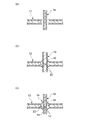
- 9 (a) to 9 (c) are schematic views showing thermal expansion and thermal contraction of the first printed circuit board 12 and the second printed circuit board 14 before and after soldering.
- FIG. 1 is a perspective view schematically showing the printed circuit board assembly 10 according to the embodiment.
- the printed circuit board assembly 10 is obtained by soldering the first printed circuit board 12 and the second printed circuit board 14 to each other and electrically connecting them.
- the first printed circuit board 12 is placed flat.
- the second printed circuit board 14 is joined to the first printed circuit board 12 at an angle (at right angles in this example) to the first printed circuit board 12. In this way, the first printed circuit board 12 and the second printed circuit board 14 are fixed to each other.
- the shapes of the first printed circuit board 12 and the second printed circuit board 14 are, for example, rectangular shapes, but the shape is not limited to this.
- the vertical and horizontal dimensions and thickness of the first printed circuit board 12 and the second printed circuit board 14 may be the same or different.
- the first printed circuit board 12 is a control circuit board for controlling the second printed circuit board 14, and the second printed circuit board 14 is a light emitting / receiving element mounting board. May be good.
- the printed circuit board assembly 10 can be used by being incorporated in a sensor device such as LiDAR (Light Detection and Ringing, Laser Imaging Detection and Ringing).
- the light emitting element (not shown) mounted on the light receiving / receiving element mounting substrate may be an infrared light emitting element such as an infrared pulsed laser light source.
- the light receiving element (not shown) mounted on the light receiving / receiving element mounting substrate may be an optical sensor capable of detecting infrared light.
- the infrared light may be near-infrared light having a wavelength selected from the range of 800 to 1550 nm.
- the first printed circuit board 12 has an elongated hole 16 penetrating the first printed circuit board 12 in the thickness direction thereof.
- the length between both ends of the elongated hole 16 (that is, the dimension in the longitudinal direction) is longer than the width of the elongated hole 16 (dimension in the lateral direction).
- the shape of the elongated hole 16 is, for example, an oval shape, but is not particularly limited thereto, and may be a rectangular or other elongated hole as long as the insertion portion 18 can be inserted.
- the second printed circuit board 14 has an insertion portion 18 to be inserted into the elongated hole 16 of the first printed circuit board 12.
- the insertion portion 18 is provided on one side of the second printed circuit board 14.
- the thickness of the insertion portion 18 (equal to the thickness of the second printed circuit board 14) is slightly smaller than the width of the insertion portion 16 so that the insertion portion 18 can be inserted into the slot 16. Is slightly smaller than the length of the slot 16.
- the width of the insertion portion 18 may be shorter than the length of one side of the second printed circuit board 14 provided with the insertion portion 18, and as shown in FIG. 1, the second printed circuit board 14 is inserted.
- Notches 20 may be provided on both sides of the portion 18.
- the width of the insertion portion 18 may be equal to or longer than the length of one side of the second printed circuit board 14.
- a plurality of (three in this example) first conductive regions 22 are provided on the surface of the first printed circuit board 12.
- each first conductive region 22 has a strip-like shape having the same width and length as each other. These first conductive regions 22 are arranged at equal intervals in the longitudinal direction of the elongated holes 16, and each of them extends in parallel from the elongated holes 16 toward one side of the first printed circuit board 12.
- Each first conductive region 22 may be a layer of a conductive material (for example, copper foil) that covers a part of the surface of the first printed circuit board 12, and is one of the circuit patterns formed on the first printed circuit board 12. It may be a department.
- each second conductive region 24 has a strip-like shape having the same width and length as each other. These second conductive regions 24 are arranged at equal intervals in the width direction of the insertion portion 18, and each extends in parallel from the insertion portion 18 toward the opposite side of the second printed circuit board 14.
- Each second conductive region 24 may be a layer of a conductive material (for example, copper foil) that covers a part of the surface of the second printed circuit board 14, and is one of the circuit patterns formed on the second printed circuit board 14. It may be a department.
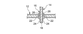
- FIG. 2 and 3 are diagrams schematically showing a solder joint portion 26 between the elongated hole 16 of the first printed circuit board 12 and the insertion portion 18 of the second printed circuit board 14 according to the embodiment.
- FIG. 2 schematically shows an AA cross section of the printed circuit board assembly 10 shown in FIG. 1
- FIG. 3 schematically shows a part of the BB cross section of FIG.
- the plurality of first conductive regions 22 described above extend not only from the surface of the first printed circuit board 12 but also from the surface to the inner peripheral surface of the elongated hole 16.
- Each first conductive region 22 covers the inner peripheral surface of the elongated hole 16 from one surface of the first printed circuit board 12 to the other surface in the thickness direction of the first printed circuit board 12 (vertical direction in FIG. 3).
- the insulating region 28 without the conductive material (for example, peeled off) and the first conductive region 22 are alternately arranged in the longitudinal direction of the elongated hole 16.
- the plurality of first conductive regions 22 are separated from each other.
- additional conductive regions 23 are formed not only on the inner peripheral surface of the elongated hole 16 facing the insertion portion 18 of the second printed circuit board 14, but also on both ends of the elongated hole 16.
- the plurality of second conductive regions 24 are provided corresponding to the plurality of first conductive regions 22.
- a plurality of first conductive regions 22 and the second conductive region 24 face each other.
- the region 22 and the plurality of second conductive regions 24 are formed on the first printed circuit board 12 and the second printed circuit board 14, respectively.
- the shape, arrangement, and number of the first conductive region 22 and the second conductive region 24 are not limited to the above-mentioned specific example, and may take various forms.
- the first conductive region 22 is provided as an electrode formed on the first printed circuit board 12 for electrical connection with the second printed circuit board 14, and the second conductive region 24 is electrically connected to the first printed circuit board 12. It is provided as an electrode formed on the second printed circuit board 14 for the purpose.
- Each first conductive region 22 is soldered to the corresponding second conductive region 24 to form a plurality of solder joints 26 in the longitudinal direction of the elongated hole 16.
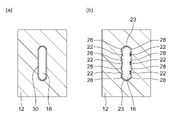
- FIGS. 4 (a) and 4 (b) are diagrams schematically showing a manufacturing method of the printed circuit board assembly 10 according to the embodiment. 4 (a) and 4 (b) schematically show a cross section corresponding to the AA cross section of the printed circuit board assembly 10 shown in FIG. 1, as in FIG. 2.
- a process of forming the elongated hole 16 and the first conductive region 22 in the first printed circuit board 12 will be described with reference to FIGS. 4 (a) and 4 (b).
- an elongated hole 16 is formed in the first printed circuit board 12.
- the elongated hole 16 is formed as a through hole, so that the entire inner peripheral surface of the elongated hole 16 is formed of the conductive material 30 from one surface of the first printed circuit board 12 to the other surface in the thickness direction of the first printed circuit board 12. It is covered.
- the conductive material 30 is, for example, a copper plating layer.
- a part of the conductive material 30 is removed from the inner peripheral surface of the elongated hole 16.
- the conductive material 30 is peeled from the inner peripheral surface of the elongated hole 16 at a plurality of locations (4 locations in this example) at intervals in the longitudinal direction of the elongated hole 16, for example, by cutting or other appropriate method.
- the portion where the conductive material 30 is lost becomes the above-mentioned insulating region 28, and the portion where the conductive material 30 remains becomes the first conductive region 22.
- the conductive material 30 is also left at both ends of the elongated hole 16 to form the conductive region 23. In this way, the elongated hole 16 and the first conductive region 22 are formed on the first printed circuit board 12.
- the insertion portion 18 of the second printed circuit board 14 is inserted into the elongated hole 16.
- the second conductive region 24 is already formed in the insertion portion 18.
- the corresponding first conductive region 22 and the second conductive region 24 are arranged facing each other.
- the first conductive region 22 and the second conductive region 24 facing each other are soldered to form a plurality of solder joints 26 in the longitudinal direction of the elongated hole 16. In this way, the first printed circuit board 12 and the second printed circuit board 14 are fixed to each other and electrically connected to each other.
- FIG. 5 is a perspective view schematically showing the printed circuit board assembly 110 according to Comparative Example 1. Similar to the printed circuit board assembly 10 according to the above-described embodiment, the printed circuit board assembly 110 shown in FIG. 5 has a first printed circuit board 112 and a second printed circuit board 114 connected at right angles to each other.
- each through hole 116 has a shape elongated along the arrangement direction of the through holes 116. In other words, each through hole 116 has an elongated shape in a direction parallel to the second printed circuit board 214 erected at a right angle to the first printed circuit board 212.
- a plurality of first conductive regions 122 are provided on the surface of the first printed circuit board 112, and each first conductive region 122 is connected to the conductive material layer of the corresponding through hole 116.
- the second printed circuit board 114 is provided with a plurality of insertion portions 118 each having a second conductive region 124. Each insertion portion 118 is inserted into the corresponding through hole 116, and the first conductive region 22 and the second conductive region 24 are soldered to each through hole 116, whereby the first printed circuit board 112 and the second printed circuit board 114 are soldered. Be joined.
- the conductive material layer connected to the first conductive region 122 covers the entire inner peripheral surface of the through hole 116 and is soldered to the second conductive region 124 facing the inner peripheral surface. Therefore, the area to be soldered can be relatively large, which is useful for improving the solder bonding strength between the two substrates.
- the pitch P of the through holes 116 (the spacing in the arrangement direction of the adjacent through holes 116) P should not be excessively narrowed, and the spacing between the adjacent first conductive regions 122 should not be excessively narrowed. It cannot be made too small. Therefore, the total length L1 in the arrangement direction of the plurality of through holes 116 tends to be long, and the joining region of the two boards including the through holes 116 and the insertion portion 118 requires a relatively large space, and in this respect. Comparative Example 1 is disadvantageous.
- FIG. 6 (a) is a perspective view schematically showing the printed circuit board assembly 210 according to Comparative Example 2
- FIG. 6 (b) is a solder joint of the printed circuit board assembly 210 shown in FIG. 6 (a). It is a figure which shows the part 226 schematically.
- the printed circuit board assembly 210 shown in FIGS. 6 (a) and 6 (b) also has a first printed circuit board 212 and a second printed circuit board 214 connected at right angles to each other.
- FIG. 6B shows a cross section of the printed circuit board assembly 210 along the thickness direction of the first printed circuit board 212, as in FIG.
- An elongated hole 216 is formed in the first printed circuit board 212, but the elongated hole 216 is merely a through hole and does not have a conductive material layer on the inner peripheral surface. Further, a plurality of first conductive regions 222 are provided on the surface of the first printed circuit board 212, and each first conductive region 122 extends to the elongated hole 216 but does not reach the inner peripheral surface of the elongated hole 216. ..
- the second printed circuit board 214 has an insertion portion 218 to be inserted into the slot 216, and the surface of the insertion portion 218 facing the inner peripheral surface of the slot 216 corresponds to a plurality of first conductive regions 222.
- a plurality of second conductive regions 224 are provided. Each first conductive region 222 is soldered to the corresponding second conductive region 224 to form a solder joint 226.
- Comparative Example 2 As shown in FIG. 6B, since the inner peripheral surface of the elongated hole 216 is not covered with the conductive material layer, the internal region of the elongated hole 216 cannot be used for soldering. ..
- the solder joint portion 226 is only formed near the surface of the first printed circuit board 212. Therefore, the area to be soldered is smaller than that of Comparative Example 1, and the solder bonding strength between the two substrates is weakened.
- Comparative Example 2 since a single elongated hole 216 is used, the hole pitch is not restricted from the strength side as in Comparative Example 1. As shown in FIG. 6A, the distance between the adjacent first conductive regions 122 can be made relatively small, and the overall length L2 in the longitudinal direction of the elongated hole 216 can be shortened. The total length L2 of the elongated hole 216 is shorter than the total length L1 of the plurality of through holes 116 of Comparative Example 1. In Comparative Example 2, the joining region of the two substrates can be made compact.
- the printed circuit board assembly 10 has the advantages of Comparative Example 1 and Comparative Example 2, improves the solder bonding strength between the two printed circuit boards, and saves the bonding area. Can be transformed into.
- each first conductive region 22 of the first printed circuit board 12 covers the inner peripheral surface of the elongated hole 16 from one surface of the first printed circuit board 12 to the other surface, the first conductive region 22 and each.
- the area of the solder joint 26 with the corresponding second conductive region 24 can be increased in the thickness direction of the substrate.
- the solder bonding strength can be improved.
- the soldering configuration of the printed circuit board assembly 10 may have other forms. An example thereof will be described below with reference to FIG.
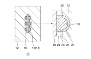
- FIG. 7 is a diagram schematically showing a solder joint portion 26 between the elongated hole 16 of the first printed circuit board 12 and the insertion portion 18 of the second printed circuit board 14 according to another embodiment.
- the printed circuit board assembly 10 according to this embodiment is different from the above-described embodiment with reference to FIGS. 1 to 3 with respect to the elongated hole 16 and the first conductive region 22 of the first printed circuit board 12, but other than that.
- the configuration is basically the same.
- FIG. 7 schematically shows a cross section of the first printed circuit board 12 along a plane.
- a plurality of first conductive regions 22 are provided on the inner peripheral surface of the elongated hole 16 in the longitudinal direction of the elongated hole 16 and are formed on the surface of the insertion portion 18 of the second printed circuit board 14 facing the inner peripheral surface of the elongated hole 16. Is provided with a plurality of second conductive regions 24 corresponding to the plurality of first conductive regions 22.
- Each first conductive region 22 covers the inner peripheral surface of the elongated hole 16 from one surface of the first printed circuit board 12 to the other surface in the thickness direction of the first printed circuit board 12.
- the first conductive region 22 and the flat portion as the insulating region 28 are alternately arranged in the longitudinal direction of the elongated hole 16, and the plurality of first conductive regions 22 are separated from each other. ..
- Each first conductive region 22 has a recess 32 facing the corresponding second conductive region 24, and is soldered to the corresponding second conductive region 24 at least in this recess 32. In this way, a plurality of solder joints 26 are formed in the longitudinal direction of the elongated holes 16.
- each recess 32 has a cylindrical surface shape extending from one surface of the first printed circuit board 12 to the other surface, but is not limited to this, and may have other appropriate recess shapes.
- FIGS. 8 (a) and 8 (b) are diagrams schematically showing a manufacturing method of the printed circuit board assembly 10 according to another embodiment. A process of forming the elongated hole 16 and the first conductive region 22 in the first printed circuit board 12 will be described with reference to FIGS. 8 (a) and 8 (b).
- each through hole 34 has a length D in a direction perpendicular to the arrangement direction longer than a width E in the arrangement direction.
- each through hole 34 has a shape elongated in a direction perpendicular to the second printed circuit board 14 erected at a right angle to the first printed circuit board 12.
- the inner peripheral surface of each through hole 34 is covered with the conductive material 30 from one surface of the first printed circuit board 12 to the other surface in the thickness direction of the first printed circuit board 12.
- an elongated hole 16 connecting a plurality of through holes 34 is formed in the first printed circuit board 12.
- the elongated hole 16 is formed so that a plurality of recesses 32 coated with the conductive material 30 are left on the inner peripheral surface of the elongated hole 16 along the longitudinal direction of the elongated hole 16.
- the conductive material 30 left in each recess 32 becomes the first conductive region 22.
- the elongated hole 16 is merely a through hole, so that the portion of the elongated hole 16 connecting the adjacent recesses 32 is not covered with the conductive material 30 and the insulating material is exposed to form an insulating region 28.
- the insertion portion 18 of the second printed circuit board 14 is inserted into the elongated hole 16.
- a plurality of second conductive regions 24 are provided on the surface of the insertion portion 18 of the second printed circuit board 14 facing the inner peripheral surface of the elongated hole 16 so as to correspond to the plurality of recesses 32.
- the first conductive region 22 and the second conductive region 24 facing each other are soldered at the recess 32, and a plurality of solder joints 26 are formed in the longitudinal direction of the elongated hole 16. In this way, the first printed circuit board 12 and the second printed circuit board 14 are fixed to each other and electrically connected to each other.
- the first conductive region 22 of the first printed circuit board 12 is the first printed circuit board 12 in the same manner as in the above-described embodiment with reference to FIGS. 1 to 3. Since the inner peripheral surface of the elongated hole 16 is covered from one surface to the other surface, the soldering area can be increased in the thickness direction of the substrate, and the solder bonding strength can be improved.
- each first conductive region 22 has a recess 32, and the second conductive region 24 and the recess 32 are soldered to form a printed circuit board associated with soldering. It is possible to mitigate the influence of the force that tends to peel off the first conductive region 22 from the inner peripheral surface of the elongated hole 16 that may be caused by thermal expansion and contraction. This also helps to improve the solder bonding strength between the two printed circuit boards.
- the plurality of through holes 34 each have an elongated shape in the direction perpendicular to the arrangement direction, it is assumed that the pitch P of the through holes 34 is the same as the pitch P of the through holes 116 of Comparative Example 1 shown in FIG. Also, the total length L3 in the longitudinal direction of the elongated hole 16 can be shortened. The total length L3 of the elongated hole 16 is shorter than the total length L1 of the plurality of through holes 116 of Comparative Example 1. Therefore, according to the embodiment, the joining region of the two substrates can be made compact.
- FIG. 9A shows a state in which the second printed circuit board 14 is inserted into the first printed circuit board 12 and these two printed circuit boards are not soldered.
- FIG. 9B shows the state of soldering the two printed circuit boards.
- the molten solder 36 heats each of the first printed circuit board 12 and the second printed circuit board 14.
- the coefficient of thermal expansion of these printed circuit boards is typically larger in the value of the coefficient of thermal expansion in the thickness direction of the substrate than in the value of the coefficient of thermal expansion in the in-plane direction of the substrate.
- the magnitude of thermal expansion of the printed circuit board generated in the thickness direction of the substrate can be several tens of times (for example, about 20 times) larger than that generated in the in-plane direction of the substrate. .. Therefore, as schematically shown by the arrow 40 in FIG. 9B, the magnitude of the thermal expansion (in the thickness direction) of the second printed circuit board 14 is the thermal expansion (in the in-plane direction) of the first printed circuit board 12. It is much larger than the size of.
- FIG. 9 (c) shows the cooling process after the soldering of the two printed circuit boards is completed. Cooling causes heat shrinkage in each of the first printed circuit board 12 and the second printed circuit board 14. Since the magnitude of this thermal shrinkage depends on the magnitude of the thermal expansion described above, the magnitude of the thermal shrinkage of the second printed circuit board 14 is the magnitude of the first printed circuit board 12 as schematically shown by the arrow 42. It is much larger than the magnitude of the heat shrinkage of.
- the thermal stress generated by these thermal shrinkages is used as a force to peel off the first conductive region 22 from the inner peripheral surface of the elongated hole 16 of the first printed circuit board 12. Or, it acts as a force to peel off the second conductive region 24 from the surface of the second printed circuit board 14.
- the adhesion strength of the conductive material layer eg, copper foil
- the thermal stress generated as a result of soldering may cause the first conductive region 22 to peel off from the elongated hole 16.
- the thermal stress acts in the direction orthogonal to the contact surface, so that the risk of peeling is considered to increase.
- the first conductive region 22 is soldered to the second conductive region 24 and the recess 32. Due to the shape of the recess 32, the contact surface between the first conductive region 22 and the first printed circuit board 12 faces in various directions depending on the location. As a result, although the thermal stress acts in the direction orthogonal to the adhesion surface in a part of the adhesion surface, the thermal stress can act in the direction parallel to the adhesion surface in other parts of the adhesion surface. When the thermal stress acts in the shear direction in this way, the static friction force acting between the first conductive region 22 and the first printed circuit board 12 can be used as a force to resist the peeling, and the yield strength to the peeling increases. .. Further, by soldering in the recess 32, it is expected that the adhesion is improved by the so-called anchor effect.
- the present invention is not limited to the above-described embodiments and modifications, and it is possible to combine embodiments and modifications, and to make further modifications such as various design changes based on the knowledge of those skilled in the art.
- the present invention also includes embodiments and modifications of such a combination, or embodiments and modifications to which further modifications are added.
- the above-mentioned embodiments and modifications, and the new embodiments resulting from the combination of the above-mentioned embodiments and modifications and the following modifications combine the effects of the combined embodiments, modifications and further modifications. Have.
- the first printed circuit board 12 and the second printed circuit board 14 are joined at a right angle, but the angle formed by the two printed circuit boards is not limited to this.
- the insertion portion 18 of the second printed circuit board 14 is inserted into the elongated hole 16 of the first printed circuit board 12 so that the first printed circuit board 12 and the second printed circuit board 14 form a desired angle, and these two printed circuit boards are inserted. It is also possible to solder.
- the desired angle may be, for example, 45 degrees or more and 90 degrees or less.
- Printed circuit board assembly 12 1st printed circuit board, 14 2nd printed circuit board, 16 long holes, 18 insertion part, 22 1st conductive area, 24 2nd conductive area, 30 conductive material, 32 recesses.
Landscapes
- Engineering & Computer Science (AREA)
- Microelectronics & Electronic Packaging (AREA)
- Manufacturing & Machinery (AREA)
- Combinations Of Printed Boards (AREA)
Abstract
プリント基板間のはんだ接合強度が向上され、接合領域が省スペース化されたプリント基板組立体を提供する。プリント基板組立体10は、長穴16を有する第1プリント基板12と、長穴16に差し込まれる差込部18を有する第2プリント基板14と、を備える。長穴16の内周面には、長穴16の長手方向に複数の第1導電領域22が設けられ、長穴16の内周面に向かい合う差込部18の表面には、複数の第1導電領域22に対応して複数の第2導電領域24が設けられている。各第1導電領域22が、第1プリント基板12の厚さ方向に第1プリント基板12の一方の表面から他方の表面にわたって長穴16の内周面を被覆しており、対応する第2導電領域24とはんだ付けされている。
Description
本発明は、プリント基板組立体およびプリント基板組立体の製造方法に関する。
従来、2枚の回路基板を直角に固定し互いに電気接続する基板固定構造が知られている(例えば、特許文献1参照。)。一方の基板には孔部が形成され、この孔部に他方の基板の脚部が挿入されて半田付けされることによって、これら2枚の基板は直角に固定される。直角に立てられた基板の両端に配置された2つの固定ホルダによって、2枚の基板間の固定が補強されている。
上記構成では、2つの固定ホルダを2枚の基板それぞれに取り付けることによって2枚の基板間の固定を補強するから、固定ホルダの設置に手間がかかる。また、固定ホルダを設けた分だけ2枚の基板の固定に要するスペースが大きくなる。
本発明はこうした状況に鑑みてなされたものであり、そのある態様の例示的な目的のひとつは、プリント基板組立体におけるプリント基板間のはんだ接合強度の向上と接合領域の省スペース化にある。
上記課題を解決するために、本発明のある態様のプリント基板組立体は、長穴を有する第1プリント基板と、長穴に差し込まれる差込部を有する第2プリント基板と、を備える。長穴の内周面には、長穴の長手方向に複数の第1導電領域が設けられ、長穴の内周面に向かい合う差込部の表面には、複数の第1導電領域に対応して複数の第2導電領域が設けられている。各第1導電領域が、第1プリント基板の厚さ方向に第1プリント基板の一方の表面から他方の表面にわたって長穴の内周面を被覆しており、対応する第2導電領域とはんだ付けされている。
この態様によると、第1プリント基板の長穴の内周面を被覆した各第1導電領域を、第2プリント基板の対応する第2導電領域とのはんだ付けに利用することができる。一方のプリント基板の片面または両面のみに設けられた導電領域に他方のプリント基板をはんだ付けする場合に比べて、はんだ付けの面積を基板の厚さ方向に大きくとることができ、はんだ接合強度を向上することができる。
また、仮に1つ1つのはんだ接合部がそれぞれ異なる穴に形成される場合には、プリント基板の強度を確保する観点から十分な穴ピッチをとるべきである。そのように十分な穴ピッチで配列された複数の穴からなる接合領域は、比較的広いスペースを要する。しかし、上記の態様によれば、1つの長穴の長手方向に第1導電領域と第2導電領域とのはんだ接合部が複数設けられるから、上述のような強度面からの穴ピッチの制約を受けない。そのため、より小さいスペースに接合領域を収めることが可能となる。
各第1導電領域は、対応する第2導電領域に向かい合う凹部を有し、少なくとも凹部で対応する第2導電領域とはんだ付けされていてもよい。このようにすれば、はんだ付けに伴うプリント基板の熱膨張と熱収縮によって生じうる、長穴の内周面から第1導電領域を引き剥がそうとする力の影響を緩和することができる。第1導電領域の長穴内周面への密着性が高まり、2枚の基板間の接合強度が向上される。
本発明の別の態様は、プリント基板組立体の製造方法である。この方法は、複数のスルーホールを第1プリント基板に形成する工程と、複数のスルーホールをつなぐ長穴を第1プリント基板に形成する工程と、長穴に第2プリント基板の差込部を差し込んで、第1プリント基板と第2プリント基板とをはんだ付けする工程と、を備える。各スルーホールの内周面は、第1プリント基板の厚さ方向に第1プリント基板の一方の表面から他方の表面にわたって導電材料で被覆される。長穴は、導電材料で被覆された複数の凹部が長穴の長手方向に沿って長穴の内周面に残されるように形成される。長穴の内周面に向かい合う第2プリント基板の差込部の表面には、複数の凹部に対応して複数の導電領域が設けられており、各凹部が、対応する導電領域とはんだ付けされる。
この態様によると、プリント基板間のはんだ接合強度が向上され、接合領域が省スペース化されたプリント基板組立体を提供することができる。
複数のスルーホールは、直線状に並んで形成されており、各スルーホールは、並び方向の幅よりも並び方向に垂直な方向の長さが長くてもよい。このように、複数のスルーホールがそれぞれ並び方向に垂直な方向に細長い形状を有する場合には、それぞれが並び方向に沿って細長い形状をもつ複数のスルーホールが形成される場合に比べて、複数のスルーホールをつなぐ長穴の長さを短くすることができる。よって、2枚のプリント基板の接合領域をより小さいスペースに収めることができる。
本発明によれば、プリント基板間のはんだ接合強度が向上され、接合領域が省スペース化されたプリント基板組立体を提供することができる。
以下、本発明を好適な実施の形態をもとに図面を参照しながら説明する。実施の形態は、発明を限定するものではなく例示であって、実施の形態に記述されるすべての特徴やその組み合わせは、必ずしも発明の本質的なものであるとは限らない。各図面に示される同一または同等の構成要素、部材、処理には、同一の符号を付するものとし、適宜重複した説明は省略する。また、各図に示す各部の縮尺や形状は、説明を容易にするために便宜的に設定されており、特に言及がない限り限定的に解釈されるものではない。また、本明細書または請求項中に用いられる「第1」、「第2」等の用語は、いかなる順序や重要度を表すものでもなく、ある構成と他の構成とを区別するためのものである。また、各図面において実施の形態を説明する上で重要ではない部材の一部は省略して表示する。
図1は、実施の形態に係るプリント基板組立体10を模式的に示す斜視図である。プリント基板組立体10は、第1プリント基板12と第2プリント基板14を互いにはんだ接合して電気接続したものである。図1において、第1プリント基板12は平置きとされている。第2プリント基板14は、第1プリント基板12に対して角度をなして(この例では直角に)第1プリント基板12に接合される。こうして、第1プリント基板12と第2プリント基板14は互いに固定される。
図1に示されるように、第1プリント基板12と第2プリント基板14の形状は例えば矩形形状であるが、これに限られない。第1プリント基板12と第2プリント基板14の縦横の寸法および厚さは、同じであってもよいし、異なっていてもよい。
プリント基板組立体10の用途の一例においては、第1プリント基板12は、第2プリント基板14を制御するための制御回路基板であり、第2プリント基板14は、受発光素子実装基板であってもよい。プリント基板組立体10は、例えばLiDAR(Light Detection and Ranging、Laser Imaging Detection and Ranging)等のセンサ機器に組み込まれて使用されうる。この場合、受発光素子実装基板に実装される発光素子(図示せず)は、例えば赤外パルスレーザー光源など、赤外発光素子であってもよい。受発光素子実装基板に実装される受光素子(図示せず)は、赤外光を検出可能な光センサであってもよい。赤外光は、800~1550nmの範囲から選択された波長を有する近赤外光であってもよい。
図1に示されるように、第1プリント基板12は、第1プリント基板12をその厚さ方向に貫通している長穴16を有する。長穴16は、その両端間の長さ(すなわち長手方向の寸法)が長穴16の幅(短手方向の寸法)に比べて長い。長穴16の形状は、例えば長円形状であるが、特にこれに限定されず、差込部18を差し込むことができる限り、矩形またはその他の形状の細長い穴であってもよい。
第2プリント基板14は、第1プリント基板12の長穴16に差し込まれる差込部18を有する。差込部18は、第2プリント基板14の一辺に設けられている。差込部18を長穴16に差し込めるように、差込部18の厚さ(第2プリント基板14の厚さに等しい)は長穴16の幅よりわずかに小さく、差込部18の幅は、長穴16の長さよりわずかに小さい。また、差込部18の幅は、差込部18が設けられた第2プリント基板14の一辺の長さより短くてもよく、図1に示されるように、第2プリント基板14は、差込部18の両側に切欠部20を有してもよい。なお、差込部18の幅は、第2プリント基板14の一辺の長さに等しくてもよく、またはそれより長くてもよい。
第1プリント基板12の表面には、複数(この例では3つ)の第1導電領域22が設けられている。一例として、各第1導電領域22は、互いに同じ幅および同じ長さをもつ短冊状の形状を有する。これら第1導電領域22は、長穴16の長手方向に等間隔に並んでおり、それぞれが長穴16から第1プリント基板12の一辺に向かって平行に延びている。各第1導電領域22は、第1プリント基板12の表面の一部を被覆する導電材料の層(例えば銅箔)であってもよく、第1プリント基板12上に形成された回路パターンの一部であってもよい。
また、第2プリント基板14の差込部18の表面には、複数(この例では3つ)の第2導電領域24が設けられている。一例として、各第2導電領域24は、互いに同じ幅および同じ長さをもつ短冊状の形状を有する。これら第2導電領域24は、差込部18の幅方向に等間隔に並んでおり、それぞれが差込部18から第2プリント基板14の反対側の辺に向かって平行に延びている。各第2導電領域24は、第2プリント基板14の表面の一部を被覆する導電材料の層(例えば銅箔)であってもよく、第2プリント基板14上に形成された回路パターンの一部であってもよい。
図2および図3は、実施の形態に係る第1プリント基板12の長穴16と第2プリント基板14の差込部18とのはんだ接合部26を模式的に示す図である。図2には、図1に示されるプリント基板組立体10のA-A断面が模式的に示され、図3には、図2のB-B断面の一部が模式的に示される。
上述の複数の第1導電領域22は、第1プリント基板12の表面だけでなく、当該表面から長穴16の内周面に延びている。各第1導電領域22は、第1プリント基板12の厚さ方向(図3の上下方向)に第1プリント基板12の一方の表面から他方の表面にわたって長穴16の内周面を被覆している。図2に示されるように、長穴16の内周面には、導電材料の無い(例えば剥離された)絶縁領域28と第1導電領域22が、長穴16の長手方向に交互に並び、複数の第1導電領域22は互いに分離されている。これは、後述する第1導電領域22の形成方法に由来するものである。同様に、長穴16の内周面のうち第2プリント基板14の差込部18に向かい合う部位だけでなく、長穴16の両端にも追加の導電領域23が形成されている。
また、複数の第2導電領域24は、複数の第1導電領域22に対応して設けられている。第2プリント基板14の差込部18が第1プリント基板12の長穴16に差し込まれたとき、対応する第1導電領域22と第2導電領域24が互いに向かい合うように、複数の第1導電領域22と複数の第2導電領域24はそれぞれ第1プリント基板12と第2プリント基板14に形成されている。なお、第1導電領域22と第2導電領域24の形状、配置、数は、上述の特定の例には限られず、様々な形態をとりうる。
第1導電領域22は、第2プリント基板14との電気接続のために第1プリント基板12上に形成された電極として設けられ、第2導電領域24は、第1プリント基板12との電気接続のために第2プリント基板14上に形成された電極として設けられている。各第1導電領域22が対応する第2導電領域24とはんだ付けされ、長穴16の長手方向に複数のはんだ接合部26が形成される。
図4(a)および図4(b)は、実施の形態に係るプリント基板組立体10の製造方法を模式的に示す図である。図4(a)および図4(b)には、図2と同様に、図1に示されるプリント基板組立体10のA-A断面に相当する断面が模式的に示される。図4(a)および図4(b)を参照して、第1プリント基板12への長穴16と第1導電領域22の形成工程を述べる。
図4(a)に示されるように、まず、第1プリント基板12に長穴16が形成される。長穴16はスルーホールとして形成され、そのため、長穴16の内周面全体が、第1プリント基板12の厚さ方向に第1プリント基板12の一方の表面から他方の表面にわたって導電材料30で被覆されている。導電材料30は例えば銅めっき層である。
次に、長穴16の内周面から導電材料30の一部が除去される。長穴16の長手方向に間隔を空けて複数箇所(この例では4箇所)で、例えば切削またはその他適宜の手法で導電材料30が長穴16の内周面から剥離される。こうして、図4(b)に示されるように、導電材料30が無くなった部位が上述の絶縁領域28となり、導電材料30が残された部位が第1導電領域22となる。この例では、導電材料30が長穴16の両端にも残され、導電領域23となる。このようにして、第1プリント基板12には、長穴16と第1導電領域22が形成される。
それから、図2に示されるように、長穴16に第2プリント基板14の差込部18が差し込まれる。差込部18には既に第2導電領域24が形成されている。対応する第1導電領域22と第2導電領域24が互いに向かい合って配置される。向かい合う第1導電領域22と第2導電領域24がはんだ付けされ、長穴16の長手方向に複数のはんだ接合部26が形成される。こうして、第1プリント基板12と第2プリント基板14が互いに固定されるとともに電気接続される。
図5は、比較例1に係るプリント基板組立体110を模式的に示す斜視図である。上述の実施の形態に係るプリント基板組立体10と同様に、図5に示されるプリント基板組立体110は、互いに直角に結合された第1プリント基板112と第2プリント基板114を有する。
ただし、第1プリント基板112には、直線状に並ぶ複数のスルーホール116が形成され、各スルーホール116は内周面全体が導電材料層で被覆されている。各スルーホール116は、スルーホール116の並び方向に沿って細長く延びた形状を有する。言い換えれば、各スルーホール116は、第1プリント基板212に直角に立てられた第2プリント基板214に平行な方向に細長い形状を有する。第1プリント基板112の表面には複数の第1導電領域122が設けられ、各第1導電領域122は対応するスルーホール116の導電材料層に接続されている。
第2プリント基板114には、各々に第2導電領域124を有する複数の差込部118が設けられている。各差込部118が対応するスルーホール116に差し込まれ、スルーホール116ごとに第1導電領域22と第2導電領域24がはんだ付けされ、それにより第1プリント基板112と第2プリント基板114が接合される。
比較例1では、第1導電領域122に接続された導電材料層がスルーホール116の内周面全体を被覆し、これに向かい合う第2導電領域124とはんだ付けされる。そのため、はんだ付けされる面積を比較的大きくとることができ、これは2枚の基板間のはんだ接合強度の向上に役立つ。
第1プリント基板112の強度を確保する観点から、スルーホール116のピッチ(隣接するスルーホール116の並び方向の間隔)Pは過剰に狭くすべきではなく、隣接する第1導電領域122の間隔をあまり小さくすることはできない。そのため、複数のスルーホール116の並び方向における全長L1は長くなりがちであり、これらスルーホール116および差込部118からなる2枚の基板の接合領域は比較的広いスペースを要し、この点で比較例1は不利である。
図6(a)は、比較例2に係るプリント基板組立体210を模式的に示す斜視図であり、図6(b)は、図6(a)に示されるプリント基板組立体210のはんだ接合部226を模式的に示す図である。図6(a)および図6(b)に示されるプリント基板組立体210も、互いに直角に結合された第1プリント基板212と第2プリント基板214を有する。なお図6(b)には、図3と同様に、第1プリント基板212の厚さ方向に沿ったプリント基板組立体210の断面が示される。
第1プリント基板212には、長穴216が形成されているが、この長穴216は、単なる貫通穴であって内周面に導電材料層を有しない。また、第1プリント基板212の表面には複数の第1導電領域222が設けられ、各第1導電領域122は長穴216まで延びているが、長穴216の内周面には達していない。
第2プリント基板214は、長穴216に差し込まれる差込部218を有し、長穴216の内周面に向かい合う差込部218の表面には、複数の第1導電領域222に対応して複数の第2導電領域224が設けられている。各第1導電領域222が対応する第2導電領域224とはんだ付けされ、はんだ接合部226が形成される。
比較例2では、図6(b)に示されるように、長穴216の内周面が導電材料層で被覆されていないため、この長穴216の内部領域をはんだ付けに利用することができない。はんだ接合部226は、第1プリント基板212の表面付近に形成されるにすぎない。そのため、比較例1に比べて、はんだ付けされる面積が小さくなり、2枚の基板間のはんだ接合強度は弱くなる。
比較例2では、単一の長穴216を用いるので、比較例1のように強度面からの穴ピッチの制約を受けない。図6(a)に示されるように、隣接する第1導電領域122の間隔を比較的小さくすることができ、長穴216の長手方向の全長L2を短くすることができる。この長穴216の全長L2は、比較例1の複数のスルーホール116の全長L1より短い。比較例2では、2枚の基板の接合領域をコンパクトにすることができる。
これに対して、実施の形態に係るプリント基板組立体10は、比較例1と比較例2の有利な点を併せ持ち、2枚のプリント基板間のはんだ接合強度を向上し、接合領域を省スペース化することができる。
つまり、第1プリント基板12の各第1導電領域22が第1プリント基板12の一方の表面から他方の表面にわたって長穴16の内周面を被覆しているので、各第1導電領域22と対応する第2導電領域24とのはんだ接合部26の面積を基板の厚さ方向に大きくすることができる。比較例2のように第1プリント基板212の片面または両面のみに設けられた第1導電領域222に第2プリント基板214をはんだ付けする場合に比べて、はんだ接合強度を向上することができる。
また、1つの長穴16の長手方向に第1導電領域22と第2導電領域24のはんだ接合部26が複数設けられるから、比較例1のように複数の穴を並べて形成する場合に考慮すべき強度上の穴ピッチの制約を受けない。そのため、より小さいスペースに接合領域を収めることが可能となる。
プリント基板組立体10のはんだ付けの構成は、他の形態もありうる。その一例を図7を参照して以下に述べる。
図7は、他の実施の形態に係る第1プリント基板12の長穴16と第2プリント基板14の差込部18とのはんだ接合部26を模式的に示す図である。この実施の形態に係るプリント基板組立体10は、図1から図3を参照して上述した実施の形態とは第1プリント基板12の長穴16と第1導電領域22に関して異なるが、その他の構成は基本的に同様である。図7には図2と同様に、第1プリント基板12の平面に沿った断面が模式的に示される。
長穴16の内周面には、長穴16の長手方向に複数の第1導電領域22が設けられ、長穴16の内周面に向かい合う第2プリント基板14の差込部18の表面には、複数の第1導電領域22に対応して複数の第2導電領域24が設けられている。各第1導電領域22が、第1プリント基板12の厚さ方向に第1プリント基板12の一方の表面から他方の表面にわたって長穴16の内周面を被覆している。長穴16の内周面には、第1導電領域22と絶縁領域28としての平坦部とが、長穴16の長手方向に交互に並び、複数の第1導電領域22は互いに分離されている。
各第1導電領域22は、対応する第2導電領域24に向かい合う凹部32を有し、少なくともこの凹部32で対応する第2導電領域24とはんだ付けされている。こうして、長穴16の長手方向に複数のはんだ接合部26が形成される。各凹部32は、この例では、第1プリント基板12の一方の表面から他方の表面へと達する円筒面状の形状を有するが、これに限定されず、その他適宜の凹部形状をとりうる。
図8(a)および図8(b)は、他の実施の形態に係るプリント基板組立体10の製造方法を模式的に示す図である。図8(a)および図8(b)を参照して、第1プリント基板12への長穴16と第1導電領域22の形成工程を述べる。
図8(a)に示されるように、まず、第1プリント基板12に複数のスルーホール34が形成される。複数のスルーホール34は、直線状に並んで形成されており、各スルーホール34は、並び方向の幅Eよりも並び方向に垂直な方向の長さDが長くなっている。言い換えれば、各スルーホール34は、第1プリント基板12に直角に立てられた第2プリント基板14に対し垂直な方向に細長く延びた形状を有する。各スルーホール34の内周面は、第1プリント基板12の厚さ方向に第1プリント基板12の一方の表面から他方の表面にわたって導電材料30で被覆されている。
次に、図8(b)に示されるように、複数のスルーホール34をつなぐ長穴16が第1プリント基板12に形成される。長穴16は、導電材料30で被覆された複数の凹部32が長穴16の長手方向に沿って長穴16の内周面に残されるように形成される。各凹部32に残された導電材料30が、第1導電領域22となる。長穴16は単なる貫通穴であり、そのため、隣接する凹部32をつなぐ長穴16の部分は導電材料30で被覆されずに絶縁材料が露出され、絶縁領域28となる。
それから、図7に示されるように、長穴16に第2プリント基板14の差込部18が差し込まれる。長穴16の内周面に向かい合う第2プリント基板14の差込部18の表面には、複数の凹部32に対応して複数の第2導電領域24が設けられている。向かい合う第1導電領域22と第2導電領域24が凹部32ではんだ付けされ、長穴16の長手方向に複数のはんだ接合部26が形成される。こうして、第1プリント基板12と第2プリント基板14が互いに固定されるとともに電気接続される。
この実施の形態に係るプリント基板組立体10も、図1から図3を参照して上述した実施の形態と同様に、第1プリント基板12の各第1導電領域22が第1プリント基板12の一方の表面から他方の表面にわたって長穴16の内周面を被覆しているので、はんだ付けの面積を基板の厚さ方向に大きくとることができ、はんだ接合強度を向上することができる。
加えて、図9を参照して後述するように、各第1導電領域22が凹部32を有し、第2導電領域24と凹部32ではんだ付けされることにより、はんだ付けに伴うプリント基板の熱膨張と熱収縮によって生じうる、第1導電領域22を長穴16の内周面から引き剥がそうとする力の影響を緩和することができる。このことも、2枚のプリント基板間のはんだ接合強度の向上に役立つ。
また、複数のスルーホール34がそれぞれ並び方向に垂直な方向に細長い形状を有するので、スルーホール34のピッチPが図5に示される比較例1のスルーホール116のピッチPと同じであったとしても、長穴16の長手方向の全長L3を短くすることができる。この長穴16の全長L3は、比較例1の複数のスルーホール116の全長L1より短い。よって、実施の形態によると、2枚の基板の接合領域をコンパクトにすることができる。
図9(a)から図9(c)は、第1プリント基板12と第2プリント基板14のはんだ付け前後の熱膨張と熱収縮を示す模式図である。図9(a)には、第1プリント基板12に第2プリント基板14が差し込まれ、これら2枚のプリント基板がはんだ付けされる前の状態が示される。
図9(b)には、2枚のプリント基板のはんだ付け時の様子が示される。このとき、溶融したはんだ36によって第1プリント基板12と第2プリント基板14それぞれが加熱される。これらプリント基板の熱膨張率は典型的に、基板の面内方向の熱膨張率の値に比べて基板の厚さ方向の熱膨張率の値のほうが大きい。はんだ36による温度上昇を考慮すると、基板の厚さ方向に生じるプリント基板の熱膨張の大きさは、基板の面内方向に生じるものと比べて、数十倍(例えば約20倍)大きくなり得る。そのため、図9(b)で矢印40により模式的に示すように、第2プリント基板14の(厚さ方向の)熱膨張の大きさが第1プリント基板12の(面内方向の)熱膨張の大きさよりもかなり大きくなる。
図9(c)には、2枚のプリント基板のはんだ付け終了後の冷却過程が示される。冷却により第1プリント基板12と第2プリント基板14それぞれに熱収縮が生じる。この熱収縮の大きさは、上述の熱膨張の大きさに応じたものとなるから、矢印42により模式的に示すように、第2プリント基板14の熱収縮の大きさが第1プリント基板12の熱収縮の大きさよりもかなり大きくなる。
はんだ接合部26は既に固体となっているから、これらの熱収縮によって生じる熱応力は、第1プリント基板12の長穴16の内周面から第1導電領域22を引き剥がそうとする力として、または、第2プリント基板14の表面から第2導電領域24を引き剥がそうとする力として働くことになる。典型的に、プリント基板のスルーホールでの導電材料層(例えば銅箔)の密着強度は、同じプリント基板の表面での導電材料層の密着強度に比べて弱い。したがって、はんだ付けの結果生じる熱応力によって、長穴16から第1導電領域22が剥離してしまうかもしれない。とりわけ、第1導電領域22が平坦である場合には、熱応力が密着面に直交する方向に働くので、剥離のリスクが高まると考えられる。
これに対して、図7に示される実施の形態では、第1導電領域22が第2導電領域24と凹部32ではんだ付けされている。凹部32の形状により、第1導電領域22と第1プリント基板12との密着面は場所により様々な方向を向いている。その結果、密着面の一部では熱応力が密着面に直交する方向に働くものの、密着面の他の部位では熱応力が密着面に平行な方向に働きうる。このように熱応力がせん断方向に働く場合、剥離に抗する力として、第1導電領域22と第1プリント基板12との間に働く静摩擦力を利用することができ、剥離への耐力が増す。また、凹部32ではんだ付けされることにより、いわゆるアンカー効果による密着性の向上も期待される。
本発明は、上述した実施の形態及び変形例に限定されるものではなく、実施の形態及び変形例を組み合わせたり、当業者の知識に基づいて各種の設計変更などのさらなる変形を加えることも可能であり、そのような組み合わせられた実施の形態や変形例、もしくはさらなる変形が加えられた実施の形態や変形例も本発明の範囲に含まれる。上述した実施の形態や変形例、及び上述した実施の形態や変形例と以下の変形との組合せによって生じる新たな実施の形態は、組み合わされる実施の形態、変形例及びさらなる変形それぞれの効果をあわせもつ。
上述の実施の形態では、第1プリント基板12と第2プリント基板14が直角に接合されているが、2枚のプリント基板がなす角度はこれに限られない。第1プリント基板12と第2プリント基板14が所望の角度をなすようにして第1プリント基板12の長穴16に第2プリント基板14の差込部18を差し込み、これら2枚のプリント基板をはんだ付けすることも可能である。所望の角度は、例えば45度以上、90度以下であってもよい。
実施の形態にもとづき、具体的な語句を用いて本発明を説明したが、実施の形態は、本発明の原理、応用の一側面を示しているにすぎず、実施の形態には、請求の範囲に規定された本発明の思想を逸脱しない範囲において、多くの変形例や配置の変更が認められる。
本国際出願は、2020年9月30日に出願された日本国特許出願である特願2020-165406号に基づく優先権を主張するものであり、当該日本国特許出願である特願2020-165406号の全内容は、本国際出願に援用される。
本発明の特定の実施の形態についての上記説明は、例示を目的として提示したものである。それらは、網羅的であったり、記載した形態そのままに本発明を制限したりすることを意図したものではない。数多くの変形や変更が、上記の記載内容に照らして可能であることは当業者に自明である。
10 プリント基板組立体、 12 第1プリント基板、 14 第2プリント基板、 16 長穴、 18 差込部、 22 第1導電領域、 24 第2導電領域、 30 導電材料、 32 凹部。
Claims (4)
- 長穴を有する第1プリント基板と、
前記長穴に差し込まれる差込部を有する第2プリント基板と、を備え、
前記長穴の内周面には、前記長穴の長手方向に複数の第1導電領域が設けられ、前記長穴の内周面に向かい合う前記差込部の表面には、前記複数の第1導電領域に対応して複数の第2導電領域が設けられ、
各第1導電領域が、前記第1プリント基板の厚さ方向に前記第1プリント基板の一方の表面から他方の表面にわたって前記長穴の内周面を被覆しており、対応する第2導電領域とはんだ付けされていることを特徴とするプリント基板組立体。 - 各第1導電領域は、前記対応する第2導電領域に向かい合う凹部を有し、少なくとも前記凹部で前記対応する第2導電領域とはんだ付けされていることを特徴とする請求項1に記載のプリント基板組立体。
- プリント基板組立体の製造方法であって、
複数のスルーホールを第1プリント基板に形成する工程と、
前記複数のスルーホールをつなぐ長穴を前記第1プリント基板に形成する工程と、
前記長穴に第2プリント基板の差込部を差し込んで、前記第1プリント基板と前記第2プリント基板とをはんだ付けする工程と、を備え、
各スルーホールの内周面は、前記第1プリント基板の厚さ方向に前記第1プリント基板の一方の表面から他方の表面にわたって導電材料で被覆され、
前記長穴は、前記導電材料で被覆された複数の凹部が前記長穴の長手方向に沿って前記長穴の内周面に残されるように形成され、
前記長穴の内周面に向かい合う前記第2プリント基板の差込部の表面には、前記複数の凹部に対応して複数の導電領域が設けられており、各凹部が、対応する導電領域とはんだ付けされることを特徴とする方法。 - 前記複数のスルーホールは、直線状に並んで形成されており、各スルーホールは、並び方向の幅よりも並び方向に垂直な方向の長さが長いことを特徴とする請求項3に記載の方法。
Applications Claiming Priority (2)
| Application Number | Priority Date | Filing Date | Title |
|---|---|---|---|
| JP2020165406A JP2022057254A (ja) | 2020-09-30 | 2020-09-30 | プリント基板組立体およびプリント基板組立体の製造方法 |
| JP2020-165406 | 2020-09-30 |
Publications (1)
| Publication Number | Publication Date |
|---|---|
| WO2022071015A1 true WO2022071015A1 (ja) | 2022-04-07 |
Family
ID=80950352
Family Applications (1)
| Application Number | Title | Priority Date | Filing Date |
|---|---|---|---|
| PCT/JP2021/034490 Ceased WO2022071015A1 (ja) | 2020-09-30 | 2021-09-21 | プリント基板組立体およびプリント基板組立体の製造方法 |
Country Status (2)
| Country | Link |
|---|---|
| JP (1) | JP2022057254A (ja) |
| WO (1) | WO2022071015A1 (ja) |
Citations (2)
| Publication number | Priority date | Publication date | Assignee | Title |
|---|---|---|---|---|
| JPS59186387A (ja) * | 1983-04-07 | 1984-10-23 | 松下電器産業株式会社 | プリント基板の接合方法 |
| JP2008109067A (ja) * | 2006-09-29 | 2008-05-08 | Toshiba Lighting & Technology Corp | プリント回路基板構造体、放電ランプ点灯装置および照明装置 |
-
2020
- 2020-09-30 JP JP2020165406A patent/JP2022057254A/ja active Pending
-
2021
- 2021-09-21 WO PCT/JP2021/034490 patent/WO2022071015A1/ja not_active Ceased
Patent Citations (2)
| Publication number | Priority date | Publication date | Assignee | Title |
|---|---|---|---|---|
| JPS59186387A (ja) * | 1983-04-07 | 1984-10-23 | 松下電器産業株式会社 | プリント基板の接合方法 |
| JP2008109067A (ja) * | 2006-09-29 | 2008-05-08 | Toshiba Lighting & Technology Corp | プリント回路基板構造体、放電ランプ点灯装置および照明装置 |
Also Published As
| Publication number | Publication date |
|---|---|
| JP2022057254A (ja) | 2022-04-11 |
Similar Documents
| Publication | Publication Date | Title |
|---|---|---|
| KR100947570B1 (ko) | 인쇄회로기판의 접속 구조체 | |
| JP4963275B2 (ja) | 配線回路基板および配線回路基板の接続構造 | |
| JP2007123428A (ja) | フレキシブル基板 | |
| JP2515948B2 (ja) | 宇宙飛行電子技術用のllccc素子の電気接続方法 | |
| JP2007324207A (ja) | プリント配線板、プリント配線板の屈曲加工方法および電子機器 | |
| JP2015015513A (ja) | Fpc基板及びその接続方法、ならびに電子部品収納用パッケージ | |
| CN114597727B (zh) | 端子固定方法 | |
| US11291120B2 (en) | Optical module | |
| WO2022071015A1 (ja) | プリント基板組立体およびプリント基板組立体の製造方法 | |
| US7234965B2 (en) | Wiring structure using flexible printed circuit board and optical module using the same | |
| JP6101112B2 (ja) | 表面実装コネクタ | |
| JP2012014919A (ja) | ピンヘッダ及び基板モジュール | |
| JP2018129465A (ja) | プリント回路基板及びプリント回路装置並びにそれらの製造方法 | |
| JP2017139394A (ja) | 電子回路基板とfpcの電気接続構造および方法 | |
| JPH0548262A (ja) | 複合形混成集積回路 | |
| JP2009044126A (ja) | テープキャリア基板および半導体装置 | |
| JP2006165079A (ja) | フレキシブルプリント基板 | |
| JPH03126290A (ja) | プリント配線板 | |
| JP2008288359A (ja) | プリント基板 | |
| JPH07142821A (ja) | プリント配線板 | |
| JP2004327605A (ja) | プリント基板の接続構造 | |
| JP2008519692A (ja) | 溶加材なしにレーザ溶接する方法、およびその方法で形成される電気装置 | |
| JP2006295078A (ja) | 主基板とフレキシブルプリント基板との接続構造及びその接続方法 | |
| JP4635641B2 (ja) | プリント回路板の接続構造 | |
| JP4410176B2 (ja) | プリント配線板 |
Legal Events
| Date | Code | Title | Description |
|---|---|---|---|
| 121 | Ep: the epo has been informed by wipo that ep was designated in this application |
Ref document number: 21875317 Country of ref document: EP Kind code of ref document: A1 |
|
| NENP | Non-entry into the national phase |
Ref country code: DE |
|
| 122 | Ep: pct application non-entry in european phase |
Ref document number: 21875317 Country of ref document: EP Kind code of ref document: A1 |