WO2022071010A1 - 高周波モジュールおよび通信装置 - Google Patents
高周波モジュールおよび通信装置 Download PDFInfo
- Publication number
- WO2022071010A1 WO2022071010A1 PCT/JP2021/034466 JP2021034466W WO2022071010A1 WO 2022071010 A1 WO2022071010 A1 WO 2022071010A1 JP 2021034466 W JP2021034466 W JP 2021034466W WO 2022071010 A1 WO2022071010 A1 WO 2022071010A1
- Authority
- WO
- WIPO (PCT)
- Prior art keywords
- semiconductor element
- amplifier circuit
- power amplifier
- high frequency
- circuit
- Prior art date
- Legal status (The legal status is an assumption and is not a legal conclusion. Google has not performed a legal analysis and makes no representation as to the accuracy of the status listed.)
- Ceased
Links
Images




Classifications
-
- H—ELECTRICITY
- H04—ELECTRIC COMMUNICATION TECHNIQUE
- H04B—TRANSMISSION
- H04B1/00—Details of transmission systems, not covered by a single one of groups H04B3/00 - H04B13/00; Details of transmission systems not characterised by the medium used for transmission
- H04B1/38—Transceivers, i.e. devices in which transmitter and receiver form a structural unit and in which at least one part is used for functions of transmitting and receiving
-
- H—ELECTRICITY
- H03—ELECTRONIC CIRCUITRY
- H03F—AMPLIFIERS
- H03F1/00—Details of amplifiers with only discharge tubes, only semiconductor devices or only unspecified devices as amplifying elements
- H03F1/56—Modifications of input or output impedances, not otherwise provided for
-
- H—ELECTRICITY
- H03—ELECTRONIC CIRCUITRY
- H03F—AMPLIFIERS
- H03F3/00—Amplifiers with only discharge tubes or only semiconductor devices as amplifying elements
- H03F3/189—High-frequency amplifiers, e.g. radio frequency amplifiers
- H03F3/19—High-frequency amplifiers, e.g. radio frequency amplifiers with semiconductor devices only
- H03F3/195—High-frequency amplifiers, e.g. radio frequency amplifiers with semiconductor devices only in integrated circuits
-
- H—ELECTRICITY
- H03—ELECTRONIC CIRCUITRY
- H03F—AMPLIFIERS
- H03F3/00—Amplifiers with only discharge tubes or only semiconductor devices as amplifying elements
- H03F3/20—Power amplifiers, e.g. Class B amplifiers, Class C amplifiers
- H03F3/21—Power amplifiers, e.g. Class B amplifiers, Class C amplifiers with semiconductor devices only
- H03F3/213—Power amplifiers, e.g. Class B amplifiers, Class C amplifiers with semiconductor devices only in integrated circuits
-
- H—ELECTRICITY
- H03—ELECTRONIC CIRCUITRY
- H03F—AMPLIFIERS
- H03F3/00—Amplifiers with only discharge tubes or only semiconductor devices as amplifying elements
- H03F3/20—Power amplifiers, e.g. Class B amplifiers, Class C amplifiers
- H03F3/24—Power amplifiers, e.g. Class B amplifiers, Class C amplifiers of transmitter output stages
- H03F3/245—Power amplifiers, e.g. Class B amplifiers, Class C amplifiers of transmitter output stages with semiconductor devices only
-
- H—ELECTRICITY
- H03—ELECTRONIC CIRCUITRY
- H03F—AMPLIFIERS
- H03F3/00—Amplifiers with only discharge tubes or only semiconductor devices as amplifying elements
- H03F3/72—Gated amplifiers, i.e. amplifiers which are rendered operative or inoperative by means of a control signal
-
- H—ELECTRICITY
- H10—SEMICONDUCTOR DEVICES; ELECTRIC SOLID-STATE DEVICES NOT OTHERWISE PROVIDED FOR
- H10W—GENERIC PACKAGES, INTERCONNECTIONS, CONNECTORS OR OTHER CONSTRUCTIONAL DETAILS OF DEVICES COVERED BY CLASS H10
- H10W70/00—Package substrates; Interposers; Redistribution layers [RDL]
- H10W70/60—Insulating or insulated package substrates; Interposers; Redistribution layers
-
- H—ELECTRICITY
- H10—SEMICONDUCTOR DEVICES; ELECTRIC SOLID-STATE DEVICES NOT OTHERWISE PROVIDED FOR
- H10W—GENERIC PACKAGES, INTERCONNECTIONS, CONNECTORS OR OTHER CONSTRUCTIONAL DETAILS OF DEVICES COVERED BY CLASS H10
- H10W90/00—Package configurations
-
- H—ELECTRICITY
- H10—SEMICONDUCTOR DEVICES; ELECTRIC SOLID-STATE DEVICES NOT OTHERWISE PROVIDED FOR
- H10W—GENERIC PACKAGES, INTERCONNECTIONS, CONNECTORS OR OTHER CONSTRUCTIONAL DETAILS OF DEVICES COVERED BY CLASS H10
- H10W99/00—Subject matter not provided for in other groups of this subclass
-
- H—ELECTRICITY
- H03—ELECTRONIC CIRCUITRY
- H03F—AMPLIFIERS
- H03F2200/00—Indexing scheme relating to amplifiers
- H03F2200/222—A circuit being added at the input of an amplifier to adapt the input impedance of the amplifier
-
- H—ELECTRICITY
- H03—ELECTRONIC CIRCUITRY
- H03F—AMPLIFIERS
- H03F2200/00—Indexing scheme relating to amplifiers
- H03F2200/294—Indexing scheme relating to amplifiers the amplifier being a low noise amplifier [LNA]
-
- H—ELECTRICITY
- H03—ELECTRONIC CIRCUITRY
- H03F—AMPLIFIERS
- H03F2200/00—Indexing scheme relating to amplifiers
- H03F2200/387—A circuit being added at the output of an amplifier to adapt the output impedance of the amplifier
-
- H—ELECTRICITY
- H03—ELECTRONIC CIRCUITRY
- H03F—AMPLIFIERS
- H03F2200/00—Indexing scheme relating to amplifiers
- H03F2200/451—Indexing scheme relating to amplifiers the amplifier being a radio frequency amplifier
-
- H—ELECTRICITY
- H03—ELECTRONIC CIRCUITRY
- H03F—AMPLIFIERS
- H03F2203/00—Indexing scheme relating to amplifiers with only discharge tubes or only semiconductor devices as amplifying elements covered by H03F3/00
- H03F2203/20—Indexing scheme relating to power amplifiers, e.g. Class B amplifiers, Class C amplifiers
- H03F2203/21—Indexing scheme relating to power amplifiers, e.g. Class B amplifiers, Class C amplifiers with semiconductor devices only
- H03F2203/211—Indexing scheme relating to power amplifiers, e.g. Class B amplifiers, Class C amplifiers with semiconductor devices only using a combination of several amplifiers
- H03F2203/21103—An impedance adaptation circuit being added at the input of a power amplifier stage
-
- H—ELECTRICITY
- H03—ELECTRONIC CIRCUITRY
- H03F—AMPLIFIERS
- H03F2203/00—Indexing scheme relating to amplifiers with only discharge tubes or only semiconductor devices as amplifying elements covered by H03F3/00
- H03F2203/20—Indexing scheme relating to power amplifiers, e.g. Class B amplifiers, Class C amplifiers
- H03F2203/21—Indexing scheme relating to power amplifiers, e.g. Class B amplifiers, Class C amplifiers with semiconductor devices only
- H03F2203/211—Indexing scheme relating to power amplifiers, e.g. Class B amplifiers, Class C amplifiers with semiconductor devices only using a combination of several amplifiers
- H03F2203/21139—An impedance adaptation circuit being added at the output of a power amplifier stage
-
- H—ELECTRICITY
- H10—SEMICONDUCTOR DEVICES; ELECTRIC SOLID-STATE DEVICES NOT OTHERWISE PROVIDED FOR
- H10W—GENERIC PACKAGES, INTERCONNECTIONS, CONNECTORS OR OTHER CONSTRUCTIONAL DETAILS OF DEVICES COVERED BY CLASS H10
- H10W70/00—Package substrates; Interposers; Redistribution layers [RDL]
- H10W70/60—Insulating or insulated package substrates; Interposers; Redistribution layers
- H10W70/62—Insulating or insulated package substrates; Interposers; Redistribution layers characterised by their interconnections
- H10W70/65—Shapes or dispositions of interconnections
- H10W70/654—Top-view layouts
- H10W70/655—Fan-out layouts
-
- H—ELECTRICITY
- H10—SEMICONDUCTOR DEVICES; ELECTRIC SOLID-STATE DEVICES NOT OTHERWISE PROVIDED FOR
- H10W—GENERIC PACKAGES, INTERCONNECTIONS, CONNECTORS OR OTHER CONSTRUCTIONAL DETAILS OF DEVICES COVERED BY CLASS H10
- H10W90/00—Package configurations
- H10W90/701—Package configurations characterised by the relative positions of pads or connectors relative to package parts
- H10W90/721—Package configurations characterised by the relative positions of pads or connectors relative to package parts of bump connectors
- H10W90/724—Package configurations characterised by the relative positions of pads or connectors relative to package parts of bump connectors between a chip and a stacked insulating package substrate, interposer or RDL
Definitions
- the present invention relates to a high frequency module and a communication device.
- a module board, a low noise amplifier, a power amplifier and a switch IC mounted on one main surface of the module board, and a plurality of ceramics mounted on the other main surface of the module board are laminated.
- a module including a low temperature co-fired ceramic component having the above structure is disclosed. With such a configuration, the module can be miniaturized.
- a metal via penetrating the laminated substrate may be connected to such a component to dissipate heat through the metal via.
- a metal via penetrating the laminated substrate may be connected to such a component to dissipate heat through the metal via.
- the laminated substrate a plurality of layers are laminated, and the length of the metal via penetrating the plurality of layers tends to be long. That is, the heat dissipation path tends to be long, and there is a possibility that sufficient heat dissipation cannot be obtained.
- an object of the present invention is to provide a high frequency module and a communication device capable of improving the heat dissipation of the laminated substrate.
- the high-frequency module comprises a laminated substrate in which a plurality of layers are laminated and has a first main surface and a second main surface, a first semiconductor element, a second semiconductor element, and a metal layer.
- the first main surface is provided with a first recess
- the first semiconductor element is mounted on the bottom surface of the first recess
- the second semiconductor element is mounted on the first main surface so as to straddle the first recess.
- the first semiconductor element is connected to a metal via penetrating from the bottom surface of the first recess to the second main surface, and the metal layer straddles the first recess between the first semiconductor element and the second semiconductor element. It is provided as follows.
- the communication device includes an RF signal processing circuit that processes high-frequency signals transmitted and received by an antenna, and the above-mentioned high-frequency module that propagates high-frequency signals between the antenna and the RF signal processing circuit. ..
- the heat dissipation of the laminated substrate can be improved.
- FIG. 1A is an external perspective view showing an example of a high frequency module according to an embodiment.
- FIG. 1B is a cross-sectional view showing an example of a high frequency module according to an embodiment.
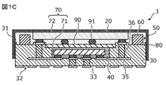
- FIG. 1C is a cross-sectional view showing another example of the high frequency module according to the embodiment.
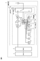
- FIG. 2 is a circuit configuration diagram showing a first example of the communication device according to the embodiment.
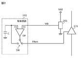
- FIG. 3 is a circuit configuration diagram showing an example of the bias adjusting circuit according to the embodiment.
- FIG. 4 is a circuit configuration diagram showing a second example of the communication device according to the embodiment.
- FIG. 5 is a circuit configuration diagram showing a third example of the communication device according to the embodiment.
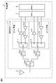
- FIG. 6 is a circuit configuration diagram showing a fourth example of the communication device according to the embodiment.
- the upper surface of the paper surface such as elements, substrates and layers is referred to as a top surface
- the lower surface of the paper surface is referred to as a bottom surface
- the lower surface of the concave surface is referred to as a bottom surface.
- FIG. 1A is an external perspective view showing an example of the high frequency module 1 according to the embodiment.
- FIG. 1B is a cross-sectional view showing an example of the high frequency module 1 according to the embodiment.
- the high frequency module 1 is, for example, a module for processing (for example, amplification, etc.) a high frequency signal.
- the high frequency module 1 includes a laminated substrate 30, a first semiconductor element 10, a second semiconductor element 20, a mounting component 60, a mold layer 70, and a shield layer 80. To prepare for. In FIG. 1A, the mold layer 70 and the shield layer 80 are made transparent.
- the laminated substrate 30 is formed by laminating a plurality of layers and has a first main surface 31 and a second main surface 32.
- Examples of the laminated substrate 30 include a low temperature co-fired ceramics (LTCC) substrate in which a plurality of dielectric layers are laminated, a high temperature co-fired ceramics (HTCC) substrate, and the like.
- LTCC low temperature co-fired ceramics
- HTCC high temperature co-fired ceramics
- RDL redistribution layer
- the first main surface 31 is provided with a terminal for mounting a component or the like on the high frequency module 1
- the second main surface 32 is provided with a terminal for mounting the high frequency module 1 on a mother board or the like.
- the first main surface 31 is provided with a first recess 40 and a second recess 50.
- the second recess 50 is shallower than the first recess 40.
- the depth refers to the size along the thickness direction of the laminated substrate 30 (the direction orthogonal to the first main surface 31 and the second main surface 32 of the laminated substrate 30).
- conductors for example, conductor film, metal vias, terminals, etc.
- Al, Cu, Au, Ag, or a metal containing an alloy thereof as a main component is used.
- the first semiconductor element 10 is substantially parallel to the bottom surface of the first recess 40 provided on the first main surface 31 of the laminated substrate 30 (the surface of the first main surface 31 of the laminated substrate 30 where the first recess 40 is not provided). It is an element mounted on a surface).
- the first semiconductor element 10 is mounted on a terminal or a conductor film provided in the first recess 40 by a solder bump or the like.
- the first semiconductor element 10 includes a power amplifier circuit.
- the power amplifier circuit included in the first semiconductor element 10 is also referred to as a first power amplifier circuit.
- the first semiconductor element 10 has a compound semiconductor substrate.
- the first semiconductor element 10 may include a first power amplifier circuit. ..
- the compound semiconductor substrate is composed of, for example, at least one of GaAs, SiGe, and GaN.
- the first power amplifier circuit excellent in amplification performance and noise performance can be realized by the first semiconductor element 10. Since the power amplifier circuit is a circuit that easily generates heat, it can be said that the first semiconductor element 10 is an element that easily generates heat. Alternatively, since the compound semiconductor substrate has poor heat dissipation, it can be said that the first semiconductor element 10 is an element that easily generates heat.
- the first semiconductor element 10 is connected to a metal via 33 penetrating from the bottom surface of the first recess 40 to the second main surface 32.
- the metal via 33 is connected to a ground terminal provided on the second main surface 32.
- the metal vias 33 may not be integrally formed, and may be formed by connecting the metal vias formed for each layer of the laminated substrate 30 to each other. Since the thickness of the portion of the laminated substrate 30 where the first recess 40 is provided is reduced by the depth of the first recess 40, the metal via 33 penetrating from the bottom surface of the first recess 40 to the second main surface 32. Is shortened by that amount.
- the second semiconductor element 20 is an element mounted on the first main surface 31 of the laminated substrate 30 so as to straddle the first recess 40 on which the first semiconductor element 10 is mounted.
- the second semiconductor element 20 may be mounted so as to cover all the first recesses 40 when the high frequency module 1 is viewed from above (when the laminated substrate 30 is viewed from the first main surface 31 side). However, it may be mounted so as to cover a part of the first recess 40. In other words, when the high frequency module 1 is viewed from above, the first recess 40 may be completely blocked by the second semiconductor element 20 so that it cannot be seen, or a part of the first recess 40 may be invisible. It may be in a state where it can be seen protruding from the semiconductor element 20.
- the second semiconductor element 20 includes at least one of a low noise amplifier circuit, a switch circuit, and a control circuit.
- the second semiconductor element 20 has a Si semiconductor substrate, and for example, by forming at least one of a low noise amplifier circuit, a switch circuit, and a control circuit on the Si semiconductor substrate, the second semiconductor element 20 is a low noise amplifier circuit. It may include at least one of a switch circuit and a control circuit.
- the Si semiconductor substrate may be an SOI substrate formed by an SOI (Silicon On Insulator) process, or may be a substrate using CMOS (Complementary Metal Oxide Semiconductor) that does not include an insulating film. This makes it possible to manufacture the second semiconductor element 20 at low cost.
- the second semiconductor element 20 is an element that is less likely to generate heat.
- the Si semiconductor substrate has better heat dissipation than the compound semiconductor substrate, it can be said that the second semiconductor element 20 is an element that does not easily generate heat.
- the metal layer 90 is provided between the first semiconductor element 10 and the second semiconductor element 20 so as to straddle the first recess 40.
- the metal layer 90 is provided so as to straddle the first recess 40, and the second semiconductor element 20 straddles the first recess 40 and the metal layer 90. Is implemented in.
- the metal layer 90 can be provided between the first semiconductor element 10 and the second semiconductor element 20 so as to straddle the first recess 40.
- the metal layer 90 is sandwiched between the first semiconductor element 10 and the second semiconductor element 20.
- the metal layer 90 may be provided so as to cover the entire first recess 40, or may be provided so as to cover a part of the first recess 40.
- the first recess 40 may be completely blocked by the metal layer 90 so that it cannot be seen, or a part of the first recess 40 is formed from the metal layer 90. It may be in a state where it can be seen protruding. Further, for example, the metal layer 90 is connected to the ground.
- the second semiconductor element 20 is connected to the metal layer 90 via a metal via 91 provided between the bottom surface of the second semiconductor element 20 and the top surface of the metal layer 90.
- the bottom surface of the second semiconductor element 20 is the surface of the second semiconductor element on the first main surface 31 side
- the top surface of the metal layer 90 is the surface of the metal layer 90 on the second semiconductor element 20 side. Since the metal layer 90 is connected to the ground, the heat generated by the second semiconductor element 20 can be dissipated to the ground.
- the laminated substrate 30 is formed at least inside the laminated substrate 30 and has a conductor that electrically connects the first semiconductor element 10 and the second semiconductor element 20.
- the laminated substrate 30 extends from the inside of the laminated substrate 30 to the bottom surface of the first recess 40 as the conductor, and is connected to the terminal of the first semiconductor element 10 at the bottom surface of the first recess 40, and the conductor film 35.
- It has a metal via 36 that is connected to the conductor film 35 inside the laminated substrate 30, extends from the conductor film 35 to the first main surface 31, and is connected to the terminal of the second semiconductor element 20 on the first main surface 31.
- the conductor enables information or signals to be exchanged between the first semiconductor element 10 and the second semiconductor element 20.
- the mounting component 60 is a surface substantially parallel to the bottom surface of the second recess 50 provided on the first main surface 31 of the laminated board 30 (the surface of the first main surface 31 of the laminated board 30 where the second recess 50 is not provided). ) Is a component mounted. For example, solder is printed on the bottom surface of the second recess 50 by a metal mask, and the mounting component 60 is mounted on the bottom surface of the second recess 50 by soldering.
- the mounting component 60 is an inductor or a capacitor constituting a matching circuit connected to an amplifier circuit or the like, a bypass capacitor connected to a control circuit 141 described later, a capacitor for DC cutting, or the like. Many of such components are relatively large in size, and the mounting component 60 has a thickness larger than that of the second semiconductor element 20.
- the mold layer 70 seals at least the second semiconductor element 20.
- the mold layer 70 has a first mold layer 71 and a second mold layer 72.
- the first mold layer 71 seals the first semiconductor element 10.
- the first mold layer 71 is a surface on the top surface of the first semiconductor element 10 (a surface opposite to the surface on the bottom surface side of the first recess 40 of the first semiconductor element 10, and is the second surface of the first semiconductor element 10. It covers the entire first semiconductor element 10 including the surface on the semiconductor element 20 side).
- the resin member to be the first mold layer 71 is injected into the first recess 40 until the top surface of the first semiconductor element 10 becomes invisible. Then, the first semiconductor element 10 can be sealed so as to cover the top surface of the first semiconductor element 10 by the first mold layer 71.
- the first mold layer 71 does not have to cover the top surface of the first semiconductor element 10.
- the resin member to be the first mold layer 71 is injected into the first recess 40 so that the top surface of the first semiconductor element 10 can be seen.
- the first semiconductor element 10 can be sealed so as not to cover the top surface of the first semiconductor element 10 with the first mold layer 71.
- the second mold layer 72 seals the second semiconductor element 20.
- the resin member to be the second mold layer 72 is mounted on the first main surface 31 so as to straddle the first recess 40 provided with the metal layer 90.
- the resin member to be the second mold layer 72 is mounted on the first main surface 31.
- the second mold layer 72 may seal the mounting component 60 mounted on the first main surface 31 together with the second semiconductor element 20.
- the resin member to be the second mold layer 72 is injected onto the first main surface 31 to form a second mold.
- the second semiconductor element 20 and the mounting component 60 can be sealed by the layer 72.
- the material of the first mold layer 71 and the material of the second mold layer 72 are different.
- the material of the first mold layer 71 may be a material that dissipates heat more easily than the material of the second mold layer 72, and the thermal conductivity of the first mold layer 71 is the thermal conductivity of the second mold layer 72. May be higher.
- the material of the second mold layer 72 may be a material that is easier to process (for example, easier to dice) than the material of the first mold layer 71.
- the material of the first mold layer 71 may be a resin containing an additive such as alumina
- the material of the second mold layer 72 may be a resin containing no additive such as alumina.
- the shield layer 80 is formed on the mold layer 70 so as to cover the mold layer 70 (second mold layer 72).
- the shield layer 80 is, for example, a metal thin film formed by a sputtering method.
- the mold layer 70 does not have to cover the top surface, which is the surface opposite to the surface on the first main surface 31 side of the second semiconductor element 20, and the shield layer 80 does not have to cover the top surface of the second semiconductor element 20. It may be in contact with the top surface. This will be described with reference to FIG. 1C.
- FIG. 1C is a cross-sectional view showing another example of the high frequency module 1 according to the embodiment.
- the mold layer 70 (second mold layer 72) does not cover the top surface of the second semiconductor element 20.
- the top surface of the mold layer 70 is, for example, chemically polished (Chemical). By polishing with mechanical polishing), the top surface of the second semiconductor element 20 can be exposed from the mold layer 70.
- the shield layer 80 is directly formed on the top surface of the second semiconductor element 20. can do. As a result, the shield layer 80 is in contact with the top surface of the second semiconductor element 20. Since the shield layer 80 is connected to the ground, for example, the heat generated by the second semiconductor element 20 can be dissipated to the ground.
- circuit configuration of communication device 1st example
- the circuit configuration of the communication device 5 including the high frequency module 1 will be described.
- FIG. 2 is a circuit configuration diagram showing a first example of the communication device 5 according to the embodiment.
- the communication device 5 includes a high frequency module 1, an antenna 2, an RF signal processing circuit (RFIC) 3, and a baseband signal processing circuit (BBIC) 4.
- RFIC RF signal processing circuit
- BBIC baseband signal processing circuit
- the RFIC 3 is an RF signal processing circuit that processes high frequency signals transmitted and received by the antenna 2. Specifically, the RFIC 3 processes the high frequency reception signal input via the reception signal path of the high frequency module 1 by down-conversion or the like, and outputs the reception signal generated by the signal processing to the BBIC 4. Further, the RFIC 3 processes the transmission signal input from the BBIC 4 by up-conversion or the like, and outputs the high frequency transmission signal generated by the signal processing to the transmission signal path of the high frequency module 1.
- the BBIC 4 is a circuit that processes a signal using an intermediate frequency band having a lower frequency than the high frequency signal propagating in the high frequency module 1.
- the signal processed by the BBIC 4 is used, for example, as an image signal for displaying an image, or as an audio signal for a call via a speaker.
- the antenna 2 is connected to the high frequency module 1 and emits a high frequency signal output from the high frequency module 1, and also receives a high frequency signal from the outside and outputs it to the high frequency module 1.
- the antenna 2 and the BBIC 4 are not essential components. That is, the communication device 5 does not have to include at least one of the antenna 2 and the BBIC 4.
- the high frequency module 1 includes a switch circuit 101, matching circuits 111, 112, 113, 114, 115 and 116, a low noise amplifier circuit 121, power amplifier circuits 131, 132 and 133, and a control circuit 141. ..
- the first semiconductor element 10 includes the power amplifier circuits 131, 132 and 133 and the matching circuits 113, 114, 115 and 116, and the second semiconductor element 20 has low noise. It includes an amplifier circuit 121, a switch circuit 101, a control circuit 141 and matching circuits 111 and 112.
- the switch circuit 101 has a common terminal and two selection terminals, the common terminal is connected to the antenna 2, one of the two selection terminals is connected to the matching circuit 111 in the received signal path, and the other.
- the selection terminal is connected to the matching circuit 113 in the transmission signal path.
- the matching circuit 111 is a circuit connected between the switch circuit 101 and the low noise amplifier circuit 121 to achieve impedance matching between the switch circuit 101 and the low noise amplifier circuit 121.
- the matching circuit 112 is a circuit connected between the low noise amplifier circuit 121 and the RFIC3 to achieve impedance matching between the low noise amplifier circuit 121 and the RFIC3.
- the matching circuit 113 is a circuit connected between the switch circuit 101 and the power amplifier circuit 131 to achieve impedance matching between the switch circuit 101 and the power amplifier circuit 131.
- the matching circuit 114 is a circuit connected between the power amplifier circuit 131 and the power amplifier circuit 132 to achieve impedance matching between the power amplifier circuit 131 and the power amplifier circuit 132.
- the matching circuit 115 is a circuit connected between the power amplifier circuit 132 and the power amplifier circuit 133 to achieve impedance matching between the power amplifier circuit 132 and the power amplifier circuit 133.
- the matching circuit 116 is a circuit connected between the power amplifier circuit 133 and the RFIC 3 to achieve impedance matching between the power amplifier circuit 133 and the RFIC 3.
- the low noise amplifier circuit 121 is an amplifier circuit that amplifies the input high frequency received signal with low noise.
- the input terminal of the low noise amplifier circuit 121 is connected to the matching circuit 111, and the output terminal of the low noise amplifier circuit 121 is connected to the matching circuit 112.
- the power amplifier circuit 131 is an amplifier circuit that amplifies the input high frequency transmission signal.
- the input terminal of the power amplifier circuit 131 is connected to the matching circuit 114, and the output terminal of the power amplifier circuit 131 is connected to the matching circuit 113.
- the power amplifier circuit 132 is an amplifier circuit that amplifies the input high frequency transmission signal.
- the input terminal of the power amplifier circuit 132 is connected to the matching circuit 115, and the output terminal of the power amplifier circuit 132 is connected to the matching circuit 114.
- the power amplifier circuit 133 is an amplifier circuit that amplifies the input high frequency transmission signal.
- the input terminal of the power amplifier circuit 133 is connected to the matching circuit 116, and the output terminal of the power amplifier circuit 133 is connected to the matching circuit 115.
- the power amplifier circuits 131, 132 and 133 are vertically connected to each other.
- the power amplifier circuit 131 is a power amplifier circuit connected to the final stage of the power amplifier circuits 131, 132, and 133 connected in sequence.
- the power amplifier circuits 131, 132 and 133 are examples of the first power amplifier circuit included in the first semiconductor element 10.
- the first semiconductor element 10 includes a detector circuit (not shown) that detects characteristic parameters of the power amplifier circuits 131, 132, and 133, and the second semiconductor element 20 is based on the characteristic parameters detected by the detector circuit. It also includes a characteristic adjustment circuit that adjusts the characteristic parameter. Since the first semiconductor element 10 and the second semiconductor element 20 are electrically connected by a conductor, the characteristic adjustment circuit can adjust the characteristic parameters based on the characteristic parameters detected by the detector circuit. It is possible.
- the characteristic parameter includes at least one of impedance, phase and power of the power amplifier circuits 131, 132 and 133.
- the detector circuit is, for example, a coupler.
- the control circuit 141 is an example of a characteristic adjustment circuit.
- the control circuit 141 is a circuit that controls a switch circuit 101, a matching circuit 111, 112, 113, 114, 115 and 116, a low noise amplifier circuit 121, and a power amplifier circuit 131, 132 and 133.
- control circuit 141 switches the connection between the antenna 2 and the received signal path and the connection between the antenna 2 and the transmitted signal path by controlling the connection between the common terminal and the two selection terminals in the switch circuit 101. ..
- each matching circuit includes one or more inductors, one or more capacitors, and one or more switches that switch the connection of each of one or more inductors and one or more capacitors.
- the control circuit 141 adjusts the connection relationship (that is, matching parameter) of one or more inductors and one or more capacitors by controlling the one or more switches, and the low noise amplifier circuit 121 to which each matching circuit is connected. Also, the input / output impedances of the power amplifier circuits 131, 132 and 133 are adjusted. Further, the control circuit 141 can adjust the phases of the low noise amplifier circuit 121 and the power amplifier circuits 131, 132 and 133 by controlling each matching circuit.
- control circuit 141 controls the gains of the low noise amplifier circuit 121 and the power amplifier circuits 131, 132 and 133. Thereby, the control circuit 141 can adjust the power of the low noise amplifier circuit 121 and the power amplifier circuits 131, 132 and 133.
- a phase device may be connected to the low noise amplifier circuit 121 and the power amplifier circuits 131, 132 and 133, and the control circuit 141 controls the phase device to control the low noise amplifier circuit 121 and the power amplifier circuit 131.
- 132 and 133 may be controlled.
- the first semiconductor element 10 includes a temperature sensor that detects the temperature of the power amplifier circuit 131, and the second semiconductor element 20 provides a bias to be supplied to the power amplifier circuit 131 based on the temperature detected by the temperature sensor. Includes a bias adjustment circuit to adjust.
- the control circuit 141 is an example of a bias adjustment circuit. This will be described with reference to FIG.
- FIG. 3 is a circuit configuration diagram showing an example of the control circuit 141 (bias adjustment circuit) according to the embodiment. Note that FIG. 3 shows a power amplifier circuit 131 and a temperature sensor 201 in addition to the control circuit 141.
- the temperature sensor 201 is thermally coupled to the power amplifier circuit 131 to generate a temperature detection signal Vdi according to the temperature of the power amplifier circuit 131. That is, the temperature sensor 201 receives (detects) the heat generated in the power amplifier circuit 131, and generates a temperature detection signal Vdi according to the temperature of the power amplifier circuit 131.
- the control circuit 141 outputs the bias control signal PAen to the power amplifier circuit 131 based on the temperature detection signal Vdi.
- the control circuit 141 includes an operational amplifier OP, a capacitor C, and a switch SW.
- a temperature sensor 201 is connected to the first input terminal T1 of the operational amplifier OP, and a capacitor C is connected to the second input terminal T2 of the operational amplifier OP.
- the switch SW is connected to the output of the operational amplifier OP, and switches between a state in which the output voltage of the operational amplifier OP is charged to the capacitor C and a state in which the output voltage is output to the power amplifier circuit 131 as a bias control signal PAen.
- the switch SW is in a state of charging the output voltage of the operational amplifier OP to the capacitor C at the start of operation of the power amplifier circuit 131.
- the voltage of the temperature detection signal Vdi input from the temperature sensor 201 to the first input terminal T1 at the start of operation of the power amplifier circuit 131 is used as the voltage indicating the reference temperature at the start of operation of the power amplifier circuit 131, and the capacitor C is used.
- the switch SW is in a state of outputting the output voltage of the operational amplifier OP to the power amplifier circuit 131 as a bias control signal PAen.
- the voltage of the temperature detection signal Vdi input from the first input terminal T1 of the operational amplifier OP and the reference temperature charged to the capacitor C input from the second input terminal T2 are shown.
- the output voltage from the operational amplifier OP which is the result of comparison with the voltage, is output to the power amplifier circuit 131 as a bias control signal PAen.
- the amplification factor increases as the voltage of the bias control signal PAen increases. Therefore, the power amplifier circuit 131 can be controlled so that the decrease in the amplification factor of the power amplifier circuit 131 due to the temperature rise is suppressed and an appropriate amplification factor is maintained by the above configuration and operation.
- control circuit 141 may be provided in the RFIC 3.
- circuit configuration of communication device 2nd example
- the power amplifier circuits 132 and 133 and the matching circuits 114, 115 and 116 connected to the power amplifier circuits 132 and 133 will be described. However, these may be included in the second semiconductor element 20. This will be described with reference to FIG. 4 as a second example of the communication device 5.
- FIG. 4 is a circuit configuration diagram showing a second example of the communication device 5 according to the embodiment.
- the first semiconductor element 10 includes a power amplifier circuit 131 and a matching circuit 113
- the second semiconductor element 20 is a low noise amplifier circuit 121, a switch circuit 101, and a control circuit.
- power amplifier circuits 132 and 133 and matching circuits 111, 112, 114, 115 and 116 are included. Since other points are the same as in the first example, the description thereof will be omitted.
- the power amplifier circuit 131 is an example of the first power amplifier circuit included in the first semiconductor element 10, and the power amplifier circuits 132 and 133 are the second semiconductor element.
- 20 is an example of a second power amplifier circuit included in 20 and connected in series with the first power amplifier circuit. As shown in FIG. 4, not all of the power amplifier circuits 131, 132 and 133 connected in cascade are formed in the first semiconductor element 10, and only the power amplifier circuit 131 in the final stage is formed in the first semiconductor element 10. , Power amplifier circuits 132 and 133 may be formed in the second semiconductor element 20.
- circuit configuration of communication device 3rd example
- the matching circuits 113 and 114 connected to the power amplifier circuit 131 are included in the first semiconductor element 10
- these are included in the laminated substrate 30. May be. This will be described with reference to FIG. 5 as a third example of the communication device 5.
- FIG. 5 is a circuit configuration diagram showing a third example of the communication device 5 according to the embodiment.
- the first semiconductor element 10 includes a power amplifier circuit 131
- the second semiconductor element 20 includes a low noise amplifier circuit 121, a switch circuit 101, a control circuit 141, and a power amplifier.
- the laminated substrate 30 includes matching circuits 113 and 114. Since other points are the same as in the first example, the description thereof will be omitted.
- the power amplifier circuit 131 is an example of the first power amplifier circuit included in the first semiconductor element 10, and the power amplifier circuits 132 and 133 are the second semiconductor element. 20 is an example of a second power amplifier circuit included in 20 and connected in series with the first power amplifier circuit.
- the matching circuits 113 and 114 connected to the power amplifier circuit 131 may not be built in the first semiconductor element 10 but may be built in the laminated substrate 30. Both the matching circuit 114 connected to the input side of the power amplifier circuit 131 and the matching circuit 113 connected to the output side of the power amplifier circuit 131 do not have to be built in the laminated board 30, and only one of them needs to be built in. It may be built in the laminated substrate 30.
- the first semiconductor element 10 may include a power amplifier circuit in a 2 GHz band
- the second semiconductor element 20 may include an amplifier circuit in a 5 GHz band
- the first semiconductor element 10 may include an amplifier circuit in the 5 GHz band
- the second semiconductor element 20 may include a power amplifier circuit in the 2 GHz band.
- the amplifier circuit may be a low noise amplifier circuit or a power amplifier circuit. This will be described with reference to FIG.
- FIG. 6 is a circuit configuration diagram showing a fourth example of the communication device 5 according to the embodiment.
- the circuit configuration of the high frequency module 1 is different from the first to third examples. Therefore, here, the circuit configuration of the high frequency module 1 in the fourth example will be mainly focused. explain.
- the high frequency module 1 includes a diplexer 301, filters 302 and 303, switch circuits 311 and 312, low noise amplifier circuits 321 and 322, and power amplifier circuits 331, 332, 333 and 334.
- the matching circuit is not shown here.
- the diplexer 301 is composed of a high-pass filter and a low-pass filter.
- a high-pass filter is a filter that passes a signal in a frequency band including at least 5 GHz band above a predetermined frequency
- a low-pass filter is a filter that passes a signal in a frequency band including at least 2 GHz band below a predetermined frequency.
- the high-pass filter is connected to the filter 302 and the low-pass filter is connected to the filter 303. Further, the high-pass filter and the low-pass filter are commonly connected to the antenna 2.
- the high-pass filter and the low-pass filter constituting the diplexer 301 are LC filters composed of an inductor, a capacitor, and the like.
- the filter 302 is arranged in the path connecting the high-pass filter and the switch circuit 311 in the diplexer 301, and passes a signal in a specific frequency band.
- the filter 302 is a filter that passes a signal in the 5 GHz band.
- the filter 303 is arranged in the path connecting the low-pass filter in the diplexer 301 and the switch circuit 312, and passes a signal in a specific frequency band.
- the filter 303 is a filter that passes a signal in the 2 GHz band.
- the filters 302 and 303 may be, for example, any of a surface acoustic wave filter, a surface acoustic wave filter using BAW (Bulk Acoustic Wave), an LC filter, and a dielectric filter, and are not limited thereto. ..
- the switch circuit 311 has a common terminal and two selection terminals, the common terminal is connected to the filter 302, one of the two selection terminals is connected to the low noise amplifier circuit 321 in the received signal path, and the other.
- the selection terminal of is connected to the power amplifier circuit 331 in the transmission signal path.
- the switch circuit 312 has a common terminal and three selection terminals, the common terminal is connected to the filter 303, and the first selection terminal of the three selection terminals is connected to the low noise amplifier circuit 322 in the received signal path.
- the 2 selection terminal is connected to the RFIC 3, and the 3rd selection terminal is connected to the power amplifier circuit 333 in the transmission signal path.
- the low noise amplifier circuit 321 is an amplifier circuit that amplifies the input high frequency received signal with low noise.
- the input terminal of the low noise amplifier circuit 321 is connected to the switch circuit 311 and the output terminal of the low noise amplifier circuit 321 is connected to the RFIC 3.
- the low noise amplifier circuit 321 is an amplifier circuit in the 5 GHz band.
- the low noise amplifier circuit 322 is an amplifier circuit that amplifies the input high frequency received signal with low noise.
- the input terminal of the low noise amplifier circuit 322 is connected to the switch circuit 312, and the output terminal of the low noise amplifier circuit 322 is connected to the RFIC 3.
- the low noise amplifier circuit 322 is an amplifier circuit in a 2 GHz band.
- the power amplifier circuit 331 is an amplifier circuit that amplifies the input high frequency transmission signal.
- the input terminal of the power amplifier circuit 331 is connected to the power amplifier circuit 332, and the output terminal of the power amplifier circuit 331 is connected to the switch circuit 311.
- the power amplifier circuit 331 is an amplifier circuit in the 5 GHz band.
- the power amplifier circuit 332 is an amplifier circuit that amplifies the input high frequency transmission signal.
- the input terminal of the power amplifier circuit 332 is connected to RFIC3, and the output terminal of the power amplifier circuit 332 is connected to the power amplifier circuit 331.
- the power amplifier circuit 332 is an amplifier circuit in the 5 GHz band.
- the power amplifier circuits 331 and 332 are connected in cascade to each other.
- the power amplifier circuit 333 is an amplifier circuit that amplifies the input high frequency transmission signal.
- the input terminal of the power amplifier circuit 333 is connected to the power amplifier circuit 334, and the output terminal of the power amplifier circuit 333 is connected to the switch circuit 312.
- the power amplifier circuit 333 is an amplifier circuit in the 2 GHz band.
- the power amplifier circuit 334 is an amplifier circuit that amplifies the input high frequency transmission signal.
- the input terminal of the power amplifier circuit 334 is connected to RFIC3, and the output terminal of the power amplifier circuit 334 is connected to the power amplifier circuit 333.
- the power amplifier circuit 334 is an amplifier circuit in a 2 GHz band.
- the power amplifier circuits 333 and 334 are connected in cascade to each other.
- the first semiconductor device 10 includes a 2 GHz band power amplifier circuit (for example, at least one of power amplifier circuits 333 and 334), and the second semiconductor element 20 includes a 5 GHz band amplifier circuit (for example, low noise amplifier circuit 321). And at least one of the power amplifier circuits 331 and 332) may be included.
- the first semiconductor element 10 includes an amplifier circuit in the 5 GHz band (for example, at least one of a low noise amplifier circuit 321 and a power amplifier circuit 331 and 332), and the second semiconductor element 20 is a power amplifier in the 2 GHz band. It may include a circuit (eg, at least one of the power amplifier circuits 333 and 334).
- the amplifier circuit that handles the signal in the 5 GHz band is included in one of the first semiconductor element 10 and the second semiconductor element 20, and the power amplifier circuit that handles the signal in the 2 GHz band is included in the first semiconductor element 10 and the second semiconductor. It may be contained in the other of the elements 20.
- the high-frequency module 1 comprises a laminated substrate 30 in which a plurality of layers are laminated and has a first main surface 31 and a second main surface 32, a first semiconductor element 10, a second semiconductor element 20, and a metal layer 90. Be prepared.
- the first main surface 31 is provided with a first recess 40.
- the first semiconductor element 10 is mounted on the bottom surface of the first recess 40, and the second semiconductor element 20 is mounted on the first main surface 31 so as to straddle the first recess 40.
- the first semiconductor element 10 is connected to a metal via 33 that penetrates from the bottom surface of the first recess 40 to the second main surface 32.
- the metal layer 90 is provided between the first semiconductor element 10 and the second semiconductor element 20 so as to straddle the first recess 40.
- the thickness of the portion of the laminated substrate 30 where the first recess 40 is provided is reduced by the depth of the first recess 40, so that the bottom surface of the first recess 40 to the second main surface 32 can be covered.
- the penetrating metal via 33 can also be shortened accordingly. That is, the heat dissipation path by the metal via 33 is shortened, and the heat dissipation property of the laminated substrate 30 can be improved. In other words, the heat generated by the first semiconductor element 10 can be effectively dissipated through the metal via 33. Further, when the metal via 33 is formed for each layer of the laminated substrate 30, the metal via 33 is shortened, so that the manufacturing time and effort and the manufacturing cost can be reduced.
- the first semiconductor element 10 is mounted in the first recess 40
- the second semiconductor element 20 is mounted on the first main surface 31 so as to straddle the first recess 40 in which the first semiconductor element 10 is mounted.
- the size of the high frequency module 1 can be reduced as compared with the case where the first semiconductor element 10 and the second semiconductor element 20 are mounted on the same plane.
- the first semiconductor element 10 mounted in the first recess 40 and the second semiconductor element 20 mounted so as to straddle the first recess 40 can be arranged so as to be vertically overlapped with each other, the first semiconductor element 10 and the second semiconductor element 20 may be in close proximity to each other. Therefore, the signal handled by the first semiconductor element 10 and the signal handled by the second semiconductor element 20 may interfere with each other, and the isolation characteristics between the first semiconductor element 10 and the second semiconductor element 20 may deteriorate. .. Therefore, by providing the metal layer 90 between the first semiconductor element 10 and the second semiconductor element 20, the interference can be suppressed, and the isolation characteristics between the first semiconductor element 10 and the second semiconductor element 20 deteriorate. Can be suppressed.
- the metal layer 90 may be connected to the ground.
- the deterioration of the isolation characteristics between the first semiconductor element 10 and the second semiconductor element 20 can be further suppressed by the metal layer 90 connected to the ground.
- the second semiconductor element 20 is provided between the bottom surface of the second semiconductor element 20 on the first main surface 31 side and the top surface of the metal layer 90 on the second semiconductor element 20 side. It may be connected to the metal layer 90 via the metal via 91.
- the heat generated in the second semiconductor element 20 is dissipated to the ground via the metal via 91 and the metal layer 90. be able to.
- the high frequency module 1 may further include a mold layer 70 for sealing at least the second semiconductor element 20 and a shield layer 80 for covering the mold layer 70.
- the shield layer 80 can suppress the entry of external noise into the high frequency module 1.
- the mold layer 70 does not have to cover the top surface, which is the surface opposite to the surface on the first main surface 31 side of the second semiconductor element 20, and the shield layer 80 does not have to cover the top surface of the second semiconductor element 20. It may be in contact with the top surface.
- the heat generated by the second semiconductor element 20 can be dissipated through the shield layer 80.
- the heat generated by the first semiconductor element 10 can be dissipated mainly from the metal via 33, and the heat generated by the second semiconductor element 20 can be dissipated mainly from the shield layer 80, and each has a different heat dissipation path. Since heat can be dissipated in, the heat generation of the high frequency module 1 can be effectively suppressed.
- the second semiconductor element 20 including the top surface is sealed by the mold layer 70, and then the mold layer 70 is formed. By polishing the top surface, the top surface of the second semiconductor element 20 is exposed. Therefore, the height of the high frequency module 1 can be reduced by the amount that the mold layer 70 is polished.
- the mold layer 70 may include a first mold layer 71 for sealing the first semiconductor element 10 and a second mold layer 72 for sealing the second semiconductor element 20, and the mold layer 70 may include the first mold layer 71.
- the material and the material of the second mold layer 72 may be different.
- the high frequency module 1 can be produced by dicing a wafer or the like in which a plurality of high frequency modules 1 are assembled.
- the material of the second mold layer 72 that seals the second semiconductor element 20 is a material that is easy to process (for example, easy to dice).
- the first mold layer 71 that seals the first semiconductor element 10 in the first recess 40 is not desired to be a material that is easy to process, and is desired to be, for example, a material that easily dissipates heat.
- the heat dissipation of the high frequency module 1 can be improved, but the wafer or the like is warped and the wafer or the like is warped. Processing may be difficult.
- the material of the first mold layer 71 and the material of the second mold layer 72 are made of the same easy-to-process material, it becomes easy to process a wafer or the like, but the heat dissipation of the high-frequency module 1 deteriorates. There is a risk. Therefore, by making the material of the first mold layer 71 different from the material of the second mold layer 72, it is possible to achieve both ease of processing and ease of heat dissipation.
- the thermal conductivity of the first mold layer 71 may be higher than the thermal conductivity of the second mold layer 72.
- the heat dissipation property in the first recess 40 of the laminated substrate 30 can be improved.
- the first semiconductor element 10 may include a power amplifier circuit in a 2 GHz band
- the second semiconductor element 20 may include an amplifier circuit in a 5 GHz band
- the first semiconductor element 10 may include an amplifier circuit in a 5 GHz band
- the second semiconductor element 20 may include a power amplifier circuit in a 2 GHz band.
- the signal in the 5 GHz band amplified in the amplifier circuit of the second semiconductor element 20 is the first. It is easily affected by a signal in the 2 GHz band that is greatly amplified by the power amplifier of the semiconductor element 10.
- the signal in the 5 GHz band amplified in the amplifier circuit of the first semiconductor element 10 is It is easily affected by the signal in the 2 GHz band that is greatly amplified in the power amplifier of the second semiconductor element 20.
- the metal layer 90 is provided between the first semiconductor element 10 and the second semiconductor element 20, the above influence can be suppressed, and the first semiconductor element 10 and the second semiconductor element 20 It is possible to suppress the deterioration of the isolation characteristics of.
- the first semiconductor element 10 may have a compound semiconductor substrate
- the second semiconductor element 20 may have a Si semiconductor substrate.
- the first semiconductor element 10 having a compound semiconductor substrate has poor heat dissipation and is more likely to generate heat than the second semiconductor element 20 having a Si semiconductor substrate.
- the first semiconductor element 10 which generates heat more easily than the second semiconductor element 20 is connected to the metal via 33 in the first recess 40, so that the second semiconductor element 20 is connected to the metal via 33 in the first recess 40. More than this, the heat generation of the high frequency module 1 can be suppressed.
- the second semiconductor element 20 may include at least one of a low noise amplifier circuit 121, a switch circuit 101, and a control circuit 141.
- the first semiconductor element 10 may include a first power amplifier circuit.
- the first semiconductor element 10 including the first power amplifier circuit is an element that generates heat more easily than the second semiconductor element 20 including at least one of the low noise amplifier circuit 121, the switch circuit 101, and the control circuit 141.
- the first semiconductor element 10 which generates heat more easily than the second semiconductor element 20 is connected to the metal via 33 in the first recess 40, so that the second semiconductor element 20 is connected to the metal via 33 in the first recess 40. More than this, the heat generation of the high frequency module 1 can be suppressed.
- the laminated substrate 30 has a conductor (for example, a conductor film 35 and a metal via 36) that is formed at least inside the laminated substrate 30 and electrically connects the first semiconductor element 10 and the second semiconductor element 20. May be.
- a conductor for example, a conductor film 35 and a metal via 36
- information or a signal can be exchanged between the first semiconductor element 10 and the second semiconductor element 20, for example, a circuit included in the first semiconductor element 10 based on the exchanged information or signal.
- the characteristics of the circuit included in the second semiconductor element 20 can be compensated.
- the conductor is formed at least inside the laminated substrate 30, the size of the high frequency module 1 is smaller than that when all the conductors are formed outside the laminated substrate 30 (for example, when wire bonding is used). It can be miniaturized.
- first semiconductor element 10 mounted in the first recess 40 and the second semiconductor element 20 mounted so as to straddle the first recess 40 can be arranged so as to be vertically overlapped with each other, the first semiconductor element The conductor connecting the 10 and the second semiconductor element 20 can be shortened, and the transmission loss in the conductor can be suppressed.
- the first semiconductor element 10 may further include a temperature sensor 201 for detecting the temperature of the first power amplifier circuit
- the second semiconductor element 20 may include the temperature sensor 201 based on the temperature detected by the temperature sensor 201.
- a control circuit 141 bias adjustment circuit for adjusting the bias supplied to the first power amplifier circuit may be included.
- the amplification factor of the first power amplifier circuit may change with the passage of time due to the heat generated by the first power amplifier circuit itself. Therefore, the bias supplied to the first power amplifier circuit is adjusted based on the temperature of the first power amplifier circuit detected by the temperature sensor 201. That is, even if the temperature of the first power amplifier circuit changes, the bias corresponding to the temperature of the first power amplifier circuit is supplied to the first power amplifier circuit, so that the amplification factor of the first power amplifier circuit is appropriate. The amplification factor can be maintained.
- the first semiconductor device 10 may further include a detector circuit for detecting the characteristic parameters of the first power amplifier circuit, and the second semiconductor element 20 may include the detector circuit based on the characteristic parameters detected by the detector circuit. It may include a characteristic adjustment circuit for adjusting characteristic parameters.
- the characteristic parameter may include at least one of the impedance, phase and power of the first power amplifier circuit.
- characteristic parameters such as impedance, phase or power of the first power amplifier circuit can be adjusted or compensated according to the situation.
- the second semiconductor element 20 may further include a second power amplifier circuit (for example, a power amplifier circuit 132 or 133) that is longitudinally connected to the first power amplifier circuit.
- a second power amplifier circuit for example, a power amplifier circuit 132 or 133
- the size of the first semiconductor element 10 can be reduced.
- the first semiconductor element 10 having a compound semiconductor substrate is often expensive, and the size of the first semiconductor element 10 can be reduced, so that the high frequency module 1 can be reduced in cost.
- the power amplifier circuit in the final stage is most likely to generate heat among the power amplifier circuits connected in series, at least the power amplifier circuit in the final stage is the first semiconductor element to which the metal via 33 is connected as the first power amplifier circuit. By including it in 10, the heat generation of the high frequency module 1 can be suppressed.
- the heat generation amount of the high frequency module 1 becomes large. It is difficult and the heat generation of the high frequency module 1 can be suppressed.
- the laminated board 30 may include a matching circuit (for example, matching circuit 113 or 114) connected to the first power amplifier circuit.
- a matching circuit for example, matching circuit 113 or 114 connected to the first power amplifier circuit.
- the size of the first semiconductor element 10 is reduced by incorporating the matching circuit connected to the first power amplifier circuit in the laminated substrate 30 instead of the first semiconductor element 10 including the first power amplifier circuit.
- the size can be reduced, and as described above, the cost of the high frequency module 1 can be reduced.
- the high frequency module 1 may further include a mounting component 60 having a thickness larger than that of the second semiconductor element 20.
- the first main surface 31 may be provided with a second recess 50, and the mounting component 60 may be mounted on the bottom surface of the second recess 50.
- the thickness of the entire high frequency module 1 is increased by the mounting component 60 having a thickness larger than that of the second semiconductor element 20. It gets thicker. Therefore, by mounting the mounting component 60 on the bottom surface of the second recess 50, it is possible to reduce the height of the high frequency module 1 by the depth of the second recess 50.
- the second recess 50 may be shallower than the first recess 40.
- the mounting component 60 for example, a chip component
- solder is printed on the laminated board 30, but if the depth of the second recess 50 is deep, the second recess 50 is printed. 2 It becomes difficult to print solder on the bottom surface of the recess 50. Therefore, by making the depth of the second recess 50 shallower than that of the first recess 40, it becomes easier to print solder on the bottom surface of the second recess 50, and the ease of mounting can be improved.
- the communication device 5 includes an RFIC 3 that processes a high-frequency signal transmitted and received by the antenna 2, and a high-frequency module 1 that propagates the high-frequency signal between the antenna 2 and the RFIC 3.
- the metal layer 90 may not be connected to the ground.
- the second semiconductor element 20 is connected to the metal layer 90 via a metal via 91 provided between the bottom surface of the second semiconductor element 20 and the top surface of the metal layer 90.
- the metal via 91 may not be provided between the bottom surface of the second semiconductor element 20 and the top surface of the metal layer 90.
- the high frequency module 1 includes the shield layer 80
- the high frequency module 1 does not have to include the shield layer 80.
- the high frequency module 1 includes the mold layer 70
- the high frequency module 1 does not have to include the mold layer 70.
- the high frequency module 1 may not include the first mold layer 71 but may include a second mold layer 72.
- the first recess 40 may be completely covered by the metal layer 90, and when the second mold layer 72 is formed, the resin member injected into the first main surface 31 fills the first recess 40. It may be prevented from flowing in.
- the high frequency module 1 may not include the second mold layer 72 but may include the first mold layer 71.
- the first semiconductor element 10 includes a first power amplifier circuit and the first semiconductor element 10 has a compound semiconductor substrate has been described, but the present invention is not limited to this.
- the first semiconductor element 10 may not include the first power amplifier circuit, and may not have the compound semiconductor substrate.
- the second semiconductor element 20 includes at least one of a low noise amplifier circuit, a switch circuit, and a control circuit, and the second semiconductor element 20 has a Si semiconductor substrate.
- the second semiconductor element 20 may not include at least one of a low noise amplifier circuit, a switch circuit, and a control circuit, and may not have a Si semiconductor substrate.
- the first semiconductor element 10 includes a temperature sensor that detects the temperature of the first power amplifier circuit, and the second semiconductor element 20 has a bias that adjusts the bias supplied to the first power amplifier circuit.
- a temperature sensor that detects the temperature of the first power amplifier circuit
- the second semiconductor element 20 has a bias that adjusts the bias supplied to the first power amplifier circuit.
- An example including an amplifier circuit has been described, but the present invention is not limited to this.
- the first semiconductor element 10 may not include the temperature sensor, and the second semiconductor element 20 may not include the bias adjustment circuit.
- the first semiconductor element 10 includes a detector circuit for detecting the characteristic parameter of the first power amplifier circuit
- the second semiconductor element 20 includes a characteristic adjustment circuit for adjusting the characteristic parameter. I explained, but it is not limited to this.
- the first semiconductor element 10 may not include a detector circuit
- the second semiconductor element 20 may not include a characteristic adjustment circuit.
- the laminated substrate 30 is formed at least inside the laminated substrate 30 and has a conductor that electrically connects the first semiconductor element 10 and the second semiconductor element 20 has been described.
- the laminated substrate 30 does not have to have a conductor that electrically connects the first semiconductor element 10 and the second semiconductor element 20.
- the conductor that electrically connects the first semiconductor element 10 and the second semiconductor element 20 may be formed on the outside of the laminated substrate 30 (for example, wire bonding may be used).
- the high frequency module 1 may not be provided with a conductor that electrically connects the first semiconductor element 10 and the second semiconductor element 20.
- the high frequency module 1 includes the mounting component 60
- the high frequency module 1 does not have to include the mounting component 60.
- the first main surface 31 of the laminated substrate 30 may not be provided with the second recess 50.
- the present invention can be widely used in devices that require heat dissipation.
Landscapes
- Engineering & Computer Science (AREA)
- Power Engineering (AREA)
- Computer Networks & Wireless Communication (AREA)
- Signal Processing (AREA)
- Microelectronics & Electronic Packaging (AREA)
- Transmitters (AREA)
- Transceivers (AREA)
- Amplifiers (AREA)
Abstract
高周波モジュール(1)は、複数の層が積層され、第1主面(31)および第2主面(32)を有する積層基板(30)と、第1半導体素子(10)と、第2半導体素子(20)と、メタル層(90)と、を備え、第1主面(31)には第1凹部(40)が設けられ、第1半導体素子(10)は、第1凹部(40)の底面に実装され、第2半導体素子(20)は、第1凹部(40)をまたぐように第1主面(31)に実装され、第1半導体素子(10)は、第1凹部(40)の底面から第2主面(32)までを貫通する金属ビア(33)と接続され、メタル層(90)は、第1半導体素子(10)と第2半導体素子(20)との間で、第1凹部(40)をまたぐように設けられる。
Description
本発明は、高周波モジュールおよび通信装置に関する。
例えば、特許文献1には、モジュール基板と、モジュール基板の一方の主面に実装されたローノイズアンプ、パワーアンプおよびスイッチICと、モジュール基板の他方の主面に実装され、複数のセラミックが積層された構造からなる低温焼成セラミック部品と、を含むモジュールが開示されている。このような構成により、モジュールの小型化が可能となっている。
特許文献1に開示されたような積層基板における部品には発熱するものがあり、このような部品に、積層基板を貫通する金属ビアが接続されて当該金属ビアを介して放熱が行われることがある。しかしながら、積層基板では、複数の層が積層されており、複数の層を貫通する金属ビアの長さが長くなりやすい。すなわち、放熱経路が長くなりやすく、十分な放熱性を得られないおそれがある。
そこで、本発明は、積層基板の放熱性を向上することができる高周波モジュールおよび通信装置を提供することを目的とする。
本発明の一態様に係る高周波モジュールは、複数の層が積層され、第1主面および第2主面を有する積層基板と、第1半導体素子と、第2半導体素子と、メタル層と、を備え、第1主面には第1凹部が設けられ、第1半導体素子は、第1凹部の底面に実装され、第2半導体素子は、第1凹部をまたぐように第1主面に実装され、第1半導体素子は、第1凹部の底面から第2主面までを貫通する金属ビアと接続され、メタル層は、第1半導体素子と第2半導体素子との間で、第1凹部をまたぐように設けられる。
本発明の一態様に係る通信装置は、アンテナで送受信される高周波信号を処理するRF信号処理回路と、アンテナとRF信号処理回路との間で高周波信号を伝搬する上記の高周波モジュールと、を備える。
本発明に係る高周波モジュール等によれば、積層基板の放熱性を向上することができる。
以下、本発明の実施の形態について、図面を用いて詳細に説明する。なお、以下で説明する実施の形態は、いずれも包括的または具体的な例を示すものである。以下の実施の形態で示される数値、形状、材料、構成要素、構成要素の配置および接続形態などは、一例であり、本発明を限定する主旨ではない。以下の実施の形態における構成要素のうち、独立請求項に記載されていない構成要素については、任意の構成要素として説明される。また、図面に示される構成要素の大きさ、または大きさの比は、必ずしも厳密ではない。また、各図において、実質的に同一の構成に対しては同一の符号を付しており、重複する説明は省略または簡略化する場合がある。また、以下の実施の形態において、「接続される」とは、直接接続される場合だけでなく、他の素子等を介して電気的に接続される場合も含まれる。
また、便宜上、以下で説明する各図面における、素子、基板および層等の紙面上側の面を天面、紙面下側の面を底面と呼び、凹部の紙面下側の面を底面と呼ぶ。
(実施の形態)
実施の形態について、以下図面を用いて説明する。
実施の形態について、以下図面を用いて説明する。
[高周波モジュールの構成]
まず、高周波モジュール1の構成について説明する。
まず、高周波モジュール1の構成について説明する。
図1Aは、実施の形態に係る高周波モジュール1の一例を示す外観斜視図である。
図1Bは、実施の形態に係る高周波モジュール1の一例を示す断面図である。
高周波モジュール1は、例えば、高周波信号を処理(例えば増幅等)するためのモジュールである。図1Aおよび図1Bに示されるように、高周波モジュール1は、積層基板30と、第1半導体素子10と、第2半導体素子20と、実装部品60と、モールド層70と、シールド層80と、を備える。なお、図1Aでは、モールド層70およびシールド層80を透明にしている。
積層基板30は、複数の層が積層されて形成され、第1主面31および第2主面32を有する。積層基板30としては、例えば、複数の誘電体層が積層されて成る低温同時焼成セラミックス(Low Temperature Co-fired Ceramics:LTCC)基板、高温同時焼成セラミックス(High Temperature Co-fired Ceramics:HTCC)基板、部品内蔵基板、再配線層(Redistribution Layer:RDL)を有する基板、または、プリント基板等が用いられる。第1主面31には、高周波モジュール1に部品等を実装するための端子が設けられ、第2主面32には、マザー基板等に高周波モジュール1を実装するための端子が設けられる。第1主面31には、第1凹部40および第2凹部50が設けられる。例えば、第2凹部50は、第1凹部40よりも深さが浅い。なお、深さとは、積層基板30の厚み方向(積層基板30の第1主面31と第2主面32に直交する方向)に沿った大きさを指す。積層基板30における各種導体(例えば導体膜、金属ビアおよび端子等)としては、例えば、Al、Cu、Au、Ag、または、これらの合金を主成分とする金属が用いられる。
第1半導体素子10は、積層基板30の第1主面31に設けられた第1凹部40の底面(積層基板30の第1主面31における第1凹部40が設けられていない面と略平行な面)に実装される素子である。例えば、第1半導体素子10は、半田バンプ等により、第1凹部40に設けられた端子または導体膜上に実装される。第1半導体素子10は、パワーアンプ回路を含む。第1半導体素子10に含まれるパワーアンプ回路を第1パワーアンプ回路とも呼ぶ。第1半導体素子10は、化合物半導体基板を有し、例えば、化合物半導体基板に第1パワーアンプ回路が形成されることで、第1半導体素子10は、第1パワーアンプ回路を含んでいてもよい。化合物半導体基板は、例えば、GaAs、SiGeおよびGaNの少なくともいずれかで構成されている。これにより、増幅性能および雑音性能に優れた第1パワーアンプ回路を第1半導体素子10によって実現することができる。パワーアンプ回路は発熱しやすい回路であるため、第1半導体素子10は、発熱しやすい素子であるといえる。あるいは、化合物半導体基板は放熱性が悪いため、第1半導体素子10は、発熱しやすい素子であるといえる。
第1半導体素子10は、第1凹部40の底面から第2主面32までを貫通する金属ビア33と接続されている。例えば、金属ビア33は、第2主面32に設けられたグランド端子に接続される。なお、金属ビア33は、一体的に形成されていなくてもよく、積層基板30の層ごとに形成された金属ビアが互いに接続されることにより、形成されていてもよい。積層基板30における第1凹部40が設けられた部分の厚みは、第1凹部40の深さ分薄くなっているため、第1凹部40の底面から第2主面32までを貫通する金属ビア33もその分短くなっている。
第2半導体素子20は、第1半導体素子10が実装された第1凹部40をまたぐように積層基板30の第1主面31に実装される素子である。なお、高周波モジュール1を上面視したときに(積層基板30を第1主面31側から見たときに)、第2半導体素子20は、第1凹部40を全て覆うように実装されてもよいし、第1凹部40の一部を覆うように実装されてもよい。言い換えると、高周波モジュール1を上面視したときに、第1凹部40が第2半導体素子20によって全て塞がれて見えない状態になっていてもよいし、第1凹部40の一部が第2半導体素子20からはみ出て見える状態になっていてもよい。第2半導体素子20は、ローノイズアンプ回路、スイッチ回路および制御回路の少なくとも1つを含む。第2半導体素子20は、Si半導体基板を有し、例えば、Si半導体基板にローノイズアンプ回路、スイッチ回路および制御回路の少なくとも1つが形成されることで、第2半導体素子20は、ローノイズアンプ回路、スイッチ回路および制御回路の少なくとも1つを含んでいてもよい。Si半導体基板は、SOI(Silicon On Insulator)プロセスにより形成されるSOI基板であってもよく、絶縁膜を内包しないCMOS(Complementary Metal Oxide Semiconductor)を用いた基板であってもよい。これにより、第2半導体素子20を安価に製造することが可能となる。ローノイズアンプ回路、スイッチ回路および制御回路は、パワーアンプ回路と比べて発熱しにくい回路であるため、第2半導体素子20は、発熱しにくい素子であるといえる。あるいは、Si半導体基板は化合物半導体基板よりも放熱性が良いため、第2半導体素子20は、発熱しにくい素子であるといえる。
メタル層90は、第1半導体素子10と第2半導体素子20との間で、第1凹部40をまたぐように設けられる。例えば、第1半導体素子10が第1凹部40に実装された後に、メタル層90が第1凹部40をまたぐように設けられ、第2半導体素子20が第1凹部40およびメタル層90をまたぐように実装される。これにより、第1半導体素子10と第2半導体素子20との間で、第1凹部40をまたぐようにメタル層90を設けることができる。高周波モジュール1を上面視したときに、第2半導体素子20、メタル層90および第1半導体素子10が重複している。言い換えると、第1半導体素子10と第2半導体素子20との間にメタル層90が挟まれている。なお、高周波モジュール1を上面視したときに、メタル層90は、第1凹部40を全て覆うように設けられてもよいし、第1凹部40の一部を覆うように設けられてもよい。言い換えると、高周波モジュール1を上面視したときに、第1凹部40がメタル層90によって全て塞がれて見えない状態になっていてもよいし、第1凹部40の一部がメタル層90からはみ出て見える状態になっていてもよい。また、例えば、メタル層90は、グランドに接続されている。
第2半導体素子20は、第2半導体素子20の底面とメタル層90の天面との間に設けられた金属ビア91を介してメタル層90と接続される。第2半導体素子20の底面は、第2半導体素子の第1主面31側の面であり、メタル層90の天面は、メタル層90の第2半導体素子20側の面である。メタル層90はグランドに接続されるため、第2半導体素子20で発生した熱をグランドへ放熱することができる。
積層基板30は、少なくとも積層基板30の内部に形成され、第1半導体素子10と第2半導体素子20とを電気的に接続する導電体を有する。例えば、積層基板30は、当該導電体として、積層基板30の内部から第1凹部40の底面へ延び、第1凹部40の底面において第1半導体素子10の端子と接続される導体膜35、および、積層基板30の内部において導体膜35と接続され、導体膜35から第1主面31へ延び、第1主面31において第2半導体素子20の端子と接続される金属ビア36を有する。当該導電体によって、第1半導体素子10と第2半導体素子20との間で情報または信号の授受が可能となる。
実装部品60は、積層基板30の第1主面31に設けられた第2凹部50の底面(積層基板30の第1主面31における第2凹部50が設けられていない面と略平行な面)に実装される部品である。例えば、第2凹部50の底面には、メタルマスクにより半田が印刷されており、実装部品60は、半田によって第2凹部50の底面に実装される。実装部品60は、アンプ回路等に接続される整合回路を構成するインダクタもしくはキャパシタ、後述する制御回路141に接続されるパスコン、または、DCカット用のキャパシタ等である。このような部品は、比較的サイズの大きいものが多く、実装部品60は、第2半導体素子20よりも大きい厚みを有する。
モールド層70は、少なくとも第2半導体素子20を封止する。例えば、ここでは、モールド層70は、第1モールド層71と、第2モールド層72とを有する。
第1モールド層71は、第1半導体素子10を封止する。例えば、第1モールド層71は、第1半導体素子10の天面(第1半導体素子10の第1凹部40の底面側の面とは反対側の面であり、第1半導体素子10の第2半導体素子20側の面)を含めて、第1半導体素子10全体を覆っている。例えば、第1凹部40に第1半導体素子10が実装された後、第1半導体素子10の天面が見えなくなるまで、第1モールド層71となる樹脂部材が第1凹部40に注入されることで、第1モールド層71によって第1半導体素子10の天面を覆うように第1半導体素子10を封止することができる。なお、第1モールド層71は、第1半導体素子10の天面を覆っていなくてもよい。この場合、第1凹部40に第1半導体素子10が実装された後、第1半導体素子10の天面が見える程度に、第1モールド層71となる樹脂部材が第1凹部40に注入されることで、第1モールド層71によって第1半導体素子10の天面を覆わないように第1半導体素子10を封止することができる。
第2モールド層72は、第2半導体素子20を封止する。例えば、第2半導体素子20が、メタル層90が設けられた第1凹部40をまたぐように第1主面31に実装された後、第2モールド層72となる樹脂部材が第1主面31上に注入されることで、第2モールド層72によって第2半導体素子20を封止することができる。例えば、第2モールド層72は、第1主面31に実装された実装部品60を第2半導体素子20と共に封止してもよい。この場合、第2半導体素子20および実装部品60が第1主面31に実装された後、第2モールド層72となる樹脂部材が第1主面31上に注入されることで、第2モールド層72によって第2半導体素子20および実装部品60を封止することができる。
第1モールド層71の材料と第2モールド層72の材料とは異なる。
例えば、第1モールド層71の材料は、第2モールド層72の材料よりも放熱しやすい材料であってもよく、第1モールド層71の熱伝導率は、第2モールド層72の熱伝導率より高くてもよい。
また、例えば、第2モールド層72の材料は、第1モールド層71の材料よりも加工しやすい(例えばダイシングしやすい)材料であってもよい。例えば、第1モールド層71の材料はアルミナなどの添加物を含む樹脂であってもよく、第2モールド層72の材料はアルミナなどの添加物を含まない樹脂であってもよい。
シールド層80は、モールド層70(第2モールド層72)を覆うようにモールド層70上に形成される。シールド層80は、例えば、スパッタ法により形成された金属薄膜である。
なお、モールド層70は、第2半導体素子20の第1主面31側の面とは反対側の面である天面を覆っていなくてもよく、シールド層80は、第2半導体素子20の天面と接触していてもよい。これについて、図1Cを用いて説明する。
図1Cは、実施の形態に係る高周波モジュール1の他の一例を示す断面図である。
図1Cに示されるように、モールド層70(第2モールド層72)は、第2半導体素子20の天面を覆っていない。製造工程において、第2半導体素子20を第2半導体素子20の天面を含めて封止するようにモールド層70が形成された時点で、モールド層70の天面を、例えば化学機械研磨(Chemical mechanical polishing)により研磨することで、第2半導体素子20の天面をモールド層70から露出させることができる。
製造工程において、シールド層80が形成される前の時点では、第2半導体素子20の天面はモールド層70から露出しているため、第2半導体素子20の天面に直接シールド層80を形成することができる。これにより、シールド層80は、第2半導体素子20の天面と接触している。シールド層80は例えばグランドに接続されるため、第2半導体素子20で発生した熱をグランドへ放熱することができる。
[通信装置の回路構成:第1例]
次に、高周波モジュール1を備える通信装置5の回路構成について説明する。
次に、高周波モジュール1を備える通信装置5の回路構成について説明する。
図2は、実施の形態に係る通信装置5の第1例を示す回路構成図である。図2に示されるように、通信装置5は、高周波モジュール1と、アンテナ2と、RF信号処理回路(RFIC)3と、ベースバンド信号処理回路(BBIC)4と、を備える。
RFIC3は、アンテナ2で送受信される高周波信号を処理するRF信号処理回路である。具体的には、RFIC3は、高周波モジュール1の受信信号経路を介して入力された高周波受信信号を、ダウンコンバートなどにより信号処理し、当該信号処理して生成された受信信号をBBIC4へ出力する。また、RFIC3は、BBIC4から入力された送信信号をアップコンバートなどにより信号処理し、当該信号処理して生成された高周波送信信号を、高周波モジュール1の送信信号経路に出力する。
BBIC4は、高周波モジュール1を伝搬する高周波信号よりも低周波の中間周波数帯域を用いて信号処理する回路である。BBIC4で処理された信号は、例えば、画像表示のための画像信号として使用され、または、スピーカを介した通話のために音声信号として使用される。
アンテナ2は、高周波モジュール1に接続され、高周波モジュール1から出力された高周波信号を放射し、また、外部からの高周波信号を受信して高周波モジュール1へ出力する。なお、本実施の形態に係る通信装置5において、アンテナ2およびBBIC4は、必須の構成要素ではない。つまり、通信装置5は、アンテナ2およびBBIC4の少なくとも一方を備えていなくてもよい。
次に、高周波モジュール1の詳細な構成について説明する。
図2に示されるように、高周波モジュール1は、スイッチ回路101、整合回路111、112、113、114、115および116、ローノイズアンプ回路121、パワーアンプ回路131、132および133ならびに制御回路141を備える。図2に示される通信装置5の第1例では、第1半導体素子10は、パワーアンプ回路131、132および133ならびに整合回路113、114、115および116を含み、第2半導体素子20は、ローノイズアンプ回路121、スイッチ回路101、制御回路141ならびに整合回路111および112を含む。
スイッチ回路101は、共通端子および2つの選択端子を有し、共通端子がアンテナ2に接続され、2つの選択端子のうちの一方の選択端子が受信信号経路における整合回路111に接続され、他方の選択端子が送信信号経路における整合回路113に接続される。
整合回路111は、スイッチ回路101とローノイズアンプ回路121との間に接続され、スイッチ回路101とローノイズアンプ回路121とのインピーダンス整合を取る回路である。
整合回路112は、ローノイズアンプ回路121とRFIC3との間に接続され、ローノイズアンプ回路121とRFIC3とのインピーダンス整合を取る回路である。
整合回路113は、スイッチ回路101とパワーアンプ回路131との間に接続され、スイッチ回路101とパワーアンプ回路131とのインピーダンス整合を取る回路である。
整合回路114は、パワーアンプ回路131とパワーアンプ回路132との間に接続され、パワーアンプ回路131とパワーアンプ回路132とのインピーダンス整合を取る回路である。
整合回路115は、パワーアンプ回路132とパワーアンプ回路133との間に接続され、パワーアンプ回路132とパワーアンプ回路133とのインピーダンス整合を取る回路である。
整合回路116は、パワーアンプ回路133とRFIC3との間に接続され、パワーアンプ回路133とRFIC3とのインピーダンス整合を取る回路である。
ローノイズアンプ回路121は、入力された高周波受信信号を低雑音で増幅する増幅回路である。ローノイズアンプ回路121の入力端子は整合回路111に接続され、ローノイズアンプ回路121の出力端子は整合回路112に接続される。
パワーアンプ回路131は、入力された高周波送信信号を増幅する増幅回路である。パワーアンプ回路131の入力端子は整合回路114に接続され、パワーアンプ回路131の出力端子は整合回路113に接続される。
パワーアンプ回路132は、入力された高周波送信信号を増幅する増幅回路である。パワーアンプ回路132の入力端子は整合回路115に接続され、パワーアンプ回路132の出力端子は整合回路114に接続される。
パワーアンプ回路133は、入力された高周波送信信号を増幅する増幅回路である。パワーアンプ回路133の入力端子は整合回路116に接続され、パワーアンプ回路133の出力端子は整合回路115に接続される。
パワーアンプ回路131、132および133は、互いに縦続接続されている。パワーアンプ回路131は、縦続接続されたパワーアンプ回路131、132および133のうち、最終段に接続されたパワーアンプ回路である。図2に示される通信装置5の第1例では、パワーアンプ回路131、132および133は、第1半導体素子10に含まれる第1パワーアンプ回路の一例である。
例えば、第1半導体素子10は、パワーアンプ回路131、132および133の特性パラメータを検知するディテクタ回路(図示せず)を含み、第2半導体素子20は、ディテクタ回路で検知された特性パラメータに基づいて、当該特性パラメータを調整する特性調整回路を含む。第1半導体素子10と第2半導体素子20とが導電体によって電気的に接続されているため、特性調整回路は、ディテクタ回路で検知された特性パラメータに基づいて、当該特性パラメータを調整することが可能となっている。特性パラメータは、パワーアンプ回路131、132および133のインピーダンス、位相および電力の少なくとも1つを含む。ディテクタ回路は、例えばカプラである。制御回路141は、特性調整回路の一例である。
制御回路141は、スイッチ回路101、整合回路111、112、113、114、115および116、ローノイズアンプ回路121ならびにパワーアンプ回路131、132および133を制御する回路である。
例えば、制御回路141は、スイッチ回路101における共通端子と2つの選択端子との接続を制御することで、アンテナ2と受信信号経路との接続、および、アンテナ2と送信信号経路との接続を切り替える。
また、例えば、各整合回路には、1以上のインダクタ、1以上のキャパシタ、ならびに、1以上のインダクタおよび1以上のキャパシタのそれぞれの接続を切り替える1以上のスイッチが含まれている。例えば、制御回路141は、当該1以上のスイッチを制御することで、1以上のインダクタおよび1以上のキャパシタの接続関係(すなわち整合パラメータ)を調整し、各整合回路が接続されたローノイズアンプ回路121ならびにパワーアンプ回路131、132および133の入出力インピーダンスを調整する。また、制御回路141は、各整合回路を制御することで、ローノイズアンプ回路121ならびにパワーアンプ回路131、132および133の位相を調整することができる。
また、例えば、制御回路141は、ローノイズアンプ回路121ならびにパワーアンプ回路131、132および133の利得を制御する。これにより、制御回路141は、ローノイズアンプ回路121ならびにパワーアンプ回路131、132および133の電力を調整することができる。
また、例えば、ローノイズアンプ回路121ならびにパワーアンプ回路131、132および133に位相器が接続されていてもよく、制御回路141は、位相器を制御することで、ローノイズアンプ回路121ならびにパワーアンプ回路131、132および133の位相を制御してもよい。
また、第1半導体素子10は、パワーアンプ回路131の温度を検知する温度センサを含み、第2半導体素子20は、温度センサで検知された温度に基づいて、パワーアンプ回路131に供給するバイアスを調整するバイアス調整回路を含む。制御回路141は、バイアス調整回路の一例である。これについて、図3を用いて説明する。
[バイアス調整回路の回路構成]
図3は、実施の形態に係る制御回路141(バイアス調整回路)の一例を示す回路構成図である。なお、図3には、制御回路141の他にパワーアンプ回路131および温度センサ201を示している。
図3は、実施の形態に係る制御回路141(バイアス調整回路)の一例を示す回路構成図である。なお、図3には、制御回路141の他にパワーアンプ回路131および温度センサ201を示している。
温度センサ201は、パワーアンプ回路131と熱的に結合して、パワーアンプ回路131の温度に応じた温度検知信号Vdiを発生する。すなわち、温度センサ201は、パワーアンプ回路131に生じる熱を受けとって(検知して)、パワーアンプ回路131の温度に応じた温度検知信号Vdiを発生する。
制御回路141は、温度検知信号Vdiに基づいて、バイアス制御信号PAenをパワーアンプ回路131へと出力する。制御回路141は、オペアンプOP、キャパシタCおよびスイッチSWを備える。オペアンプOPの第1入力端子T1には温度センサ201が接続され、オペアンプOPの第2入力端子T2にはキャパシタCが接続されている。スイッチSWは、オペアンプOPの出力に接続され、オペアンプOPの出力電圧を、キャパシタCへチャージする状態と、パワーアンプ回路131へバイアス制御信号PAenとして出力する状態とを切り替える。
まず、スイッチSWはパワーアンプ回路131の動作開始時にオペアンプOPの出力電圧をキャパシタCへチャージする状態となる。言い換えれば、パワーアンプ回路131の動作開始時に温度センサ201から第1入力端子T1に入力された温度検知信号Vdiの電圧を、パワーアンプ回路131の動作開始時の基準温度を示す電圧として、キャパシタCへチャージする。次に、スイッチSWはオペアンプOPの出力電圧をパワーアンプ回路131へバイアス制御信号PAenとして出力する状態となる。すなわち、パワーアンプ回路131の動作開始後、オペアンプOPの第1入力端子T1から都度入力される温度検知信号Vdiの電圧と第2入力端子T2から入力されるキャパシタCにチャージされた基準温度を示す電圧とを比較した結果であるオペアンプOPからの出力電圧を、パワーアンプ回路131へバイアス制御信号PAenとして出力する。
パワーアンプ回路131は、上記バイアス制御信号PAenの電圧が上昇するほど増幅率が増大する。そのため、上記構成および作用によって、温度上昇に伴うパワーアンプ回路131の増幅率の低下が抑制されて適正な増幅率が維持されるようにパワーアンプ回路131を制御できる。
なお、制御回路141の機能の全てまたは一部は、RFIC3に設けられていてもよい。
[通信装置の回路構成:第2例]
図2に示される通信装置5の第1例では、パワーアンプ回路132および133ならびにパワーアンプ回路132および133に接続された整合回路114、115および116が第1半導体素子10に含まれる例について説明したが、これらが第2半導体素子20に含まれていてもよい。これについて、通信装置5の第2例として図4を用いて説明する。
図2に示される通信装置5の第1例では、パワーアンプ回路132および133ならびにパワーアンプ回路132および133に接続された整合回路114、115および116が第1半導体素子10に含まれる例について説明したが、これらが第2半導体素子20に含まれていてもよい。これについて、通信装置5の第2例として図4を用いて説明する。
図4は、実施の形態に係る通信装置5の第2例を示す回路構成図である。
図4に示される通信装置5の第2例では、第1半導体素子10は、パワーアンプ回路131および整合回路113を含み、第2半導体素子20は、ローノイズアンプ回路121、スイッチ回路101、制御回路141、パワーアンプ回路132および133ならびに整合回路111、112、114、115および116を含む。その他の点については、第1例と同じであるため、説明を省略する。
図4に示される通信装置5の第2例では、パワーアンプ回路131は、第1半導体素子10に含まれる第1パワーアンプ回路の一例であり、パワーアンプ回路132および133は、第2半導体素子20に含まれ、第1パワーアンプ回路と縦続接続される第2パワーアンプ回路の一例である。図4に示されるように、縦続接続されたパワーアンプ回路131、132および133の全てが第1半導体素子10に形成されず、最終段のパワーアンプ回路131のみが第1半導体素子10に形成され、パワーアンプ回路132および133が第2半導体素子20に形成されてもよい。
[通信装置の回路構成:第3例]
図2に示される通信装置5の第1例では、パワーアンプ回路131に接続された整合回路113および114が第1半導体素子10に含まれる例について説明したが、これらが積層基板30に含まれていてもよい。これについて、通信装置5の第3例として図5を用いて説明する。
図2に示される通信装置5の第1例では、パワーアンプ回路131に接続された整合回路113および114が第1半導体素子10に含まれる例について説明したが、これらが積層基板30に含まれていてもよい。これについて、通信装置5の第3例として図5を用いて説明する。
図5は、実施の形態に係る通信装置5の第3例を示す回路構成図である。
図5に示される通信装置5の第3例では、第1半導体素子10は、パワーアンプ回路131を含み、第2半導体素子20は、ローノイズアンプ回路121、スイッチ回路101、制御回路141、パワーアンプ回路132および133ならびに整合回路111、112、115および116を含み、積層基板30は、整合回路113および114を含む。その他の点については、第1例と同じであるため、説明を省略する。
図5に示される通信装置5の第3例では、パワーアンプ回路131は、第1半導体素子10に含まれる第1パワーアンプ回路の一例であり、パワーアンプ回路132および133は、第2半導体素子20に含まれ、第1パワーアンプ回路と縦続接続される第2パワーアンプ回路の一例である。図5に示されるように、パワーアンプ回路131に接続される整合回路113および114が第1半導体素子10に内蔵されず、積層基板30に内蔵されてもよい。なお、パワーアンプ回路131の入力側に接続された整合回路114およびパワーアンプ回路131の出力側に接続された整合回路113の両方が積層基板30に内蔵されなくてもよく、いずれか一方のみが積層基板30に内蔵されていてもよい。
[通信装置の回路構成:第4例]
例えば、第1半導体素子10は、2GHz帯域のパワーアンプ回路を含み、第2半導体素子20は、5GHz帯域の増幅回路を含んでいてもよい。あるいは、第1半導体素子10は、5GHz帯域の増幅回路を含み、第2半導体素子20は、2GHz帯域のパワーアンプ回路を含んでいてもよい。増幅回路は、ローノイズアンプ回路であってもよいし、パワーアンプ回路であってもよい。これについて、図6を用いて説明する。
例えば、第1半導体素子10は、2GHz帯域のパワーアンプ回路を含み、第2半導体素子20は、5GHz帯域の増幅回路を含んでいてもよい。あるいは、第1半導体素子10は、5GHz帯域の増幅回路を含み、第2半導体素子20は、2GHz帯域のパワーアンプ回路を含んでいてもよい。増幅回路は、ローノイズアンプ回路であってもよいし、パワーアンプ回路であってもよい。これについて、図6を用いて説明する。
図6は、実施の形態に係る通信装置5の第4例を示す回路構成図である。図6に示される通信装置5の第4例では、高周波モジュール1の回路構成が第1例から第3例と異なっているため、ここでは、第4例における高周波モジュール1の回路構成を中心に説明する。
第4例では、高周波モジュール1は、ダイプレクサ301、フィルタ302および303、スイッチ回路311および312、ローノイズアンプ回路321および322、ならびに、パワーアンプ回路331、332、333および334を備える。なお、ここでは、整合回路の図示を省略している。
ダイプレクサ301は、ハイパスフィルタおよびローパスフィルタから構成される。ハイパスフィルタは所定の周波数以上の、少なくとも5GHz帯域を含む周波数帯域の信号を通過させるフィルタであり、ローパスフィルタは所定の周波数未満の、少なくとも2GHz帯域を含む周波数帯域の信号を通過させるフィルタである。ハイパスフィルタはフィルタ302に接続され、ローパスフィルタはフィルタ303に接続される。また、ハイパスフィルタおよびローパスフィルタは、共通してアンテナ2に接続される。例えば、ダイプレクサ301を構成するハイパスフィルタおよびローパスフィルタは、インダクタおよびキャパシタ等で構成されたLCフィルタである。
フィルタ302は、ダイプレクサ301におけるハイパスフィルタとスイッチ回路311とを結ぶ経路に配置され、特定の周波数帯域の信号を通過させる。例えば、フィルタ302は、5GHz帯域の信号を通過させるフィルタである。
フィルタ303は、ダイプレクサ301におけるローパスフィルタとスイッチ回路312とを結ぶ経路に配置され、特定の周波数帯域の信号を通過させる。例えば、フィルタ303は、2GHz帯域の信号を通過させるフィルタである。
なお、フィルタ302および303は、例えば、弾性表面波フィルタ、BAW(Bulk Acoustic Wave)を用いた弾性波フィルタ、LCフィルタおよび誘電体フィルタのいずれであってもよく、さらには、これらには限定されない。
スイッチ回路311は、共通端子および2つの選択端子を有し、共通端子がフィルタ302に接続され、2つの選択端子のうちの一方の選択端子が受信信号経路におけるローノイズアンプ回路321に接続され、他方の選択端子が送信信号経路におけるパワーアンプ回路331に接続される。
スイッチ回路312は、共通端子および3つの選択端子を有し、共通端子がフィルタ303に接続され、3つの選択端子のうちの第1選択端子が受信信号経路におけるローノイズアンプ回路322に接続され、第2選択端子がRFIC3に接続され、第3選択端子が送信信号経路におけるパワーアンプ回路333に接続される。
ローノイズアンプ回路321は、入力された高周波受信信号を低雑音で増幅する増幅回路である。ローノイズアンプ回路321の入力端子はスイッチ回路311に接続され、ローノイズアンプ回路321の出力端子はRFIC3に接続される。ローノイズアンプ回路321は、5GHz帯域の増幅回路である。
ローノイズアンプ回路322は、入力された高周波受信信号を低雑音で増幅する増幅回路である。ローノイズアンプ回路322の入力端子はスイッチ回路312に接続され、ローノイズアンプ回路322の出力端子はRFIC3に接続される。ローノイズアンプ回路322は、2GHz帯域の増幅回路である。
パワーアンプ回路331は、入力された高周波送信信号を増幅する増幅回路である。パワーアンプ回路331の入力端子はパワーアンプ回路332に接続され、パワーアンプ回路331の出力端子はスイッチ回路311に接続される。パワーアンプ回路331は、5GHz帯域の増幅回路である。
パワーアンプ回路332は、入力された高周波送信信号を増幅する増幅回路である。パワーアンプ回路332の入力端子はRFIC3に接続され、パワーアンプ回路332の出力端子はパワーアンプ回路331に接続される。パワーアンプ回路332は、5GHz帯域の増幅回路である。パワーアンプ回路331および332は、互いに縦続接続されている。
パワーアンプ回路333は、入力された高周波送信信号を増幅する増幅回路である。パワーアンプ回路333の入力端子はパワーアンプ回路334に接続され、パワーアンプ回路333の出力端子はスイッチ回路312に接続される。パワーアンプ回路333は、2GHz帯域の増幅回路である。
パワーアンプ回路334は、入力された高周波送信信号を増幅する増幅回路である。パワーアンプ回路334の入力端子はRFIC3に接続され、パワーアンプ回路334の出力端子はパワーアンプ回路333に接続される。パワーアンプ回路334は、2GHz帯域の増幅回路である。パワーアンプ回路333および334は、互いに縦続接続されている。
例えば、第1半導体素子10は、2GHz帯域のパワーアンプ回路(例えばパワーアンプ回路333および334の少なくとも1つ)を含み、第2半導体素子20は、5GHz帯域の増幅回路(例えば、ローノイズアンプ回路321ならびにパワーアンプ回路331および332の少なくとも1つ)を含んでいてもよい。あるいは、例えば、第1半導体素子10は、5GHz帯域の増幅回路(例えば、ローノイズアンプ回路321ならびにパワーアンプ回路331および332の少なくとも1つ)を含み、第2半導体素子20は、2GHz帯域のパワーアンプ回路(例えばパワーアンプ回路333および334の少なくとも1つ)を含んでいてもよい。すなわち、5GHz帯域の信号を扱う増幅回路が、第1半導体素子10および第2半導体素子20のうちの一方に含まれ、2GHz帯域の信号を扱うパワーアンプ回路が第1半導体素子10および第2半導体素子20のうちの他方に含まれていてもよい。
[まとめ]
高周波モジュール1は、複数の層が積層され、第1主面31および第2主面32を有する積層基板30と、第1半導体素子10と、第2半導体素子20と、メタル層90と、を備える。第1主面31には第1凹部40が設けられる。第1半導体素子10は、第1凹部40の底面に実装され、第2半導体素子20は、第1凹部40をまたぐように第1主面31に実装される。第1半導体素子10は、第1凹部40の底面から第2主面32までを貫通する金属ビア33と接続されている。メタル層90は、第1半導体素子10と第2半導体素子20との間で、第1凹部40をまたぐように設けられる。
高周波モジュール1は、複数の層が積層され、第1主面31および第2主面32を有する積層基板30と、第1半導体素子10と、第2半導体素子20と、メタル層90と、を備える。第1主面31には第1凹部40が設けられる。第1半導体素子10は、第1凹部40の底面に実装され、第2半導体素子20は、第1凹部40をまたぐように第1主面31に実装される。第1半導体素子10は、第1凹部40の底面から第2主面32までを貫通する金属ビア33と接続されている。メタル層90は、第1半導体素子10と第2半導体素子20との間で、第1凹部40をまたぐように設けられる。
これによれば、積層基板30における第1凹部40が設けられた部分の厚みは、第1凹部40の深さ分薄くなっているため、第1凹部40の底面から第2主面32までを貫通する金属ビア33もその分短くすることができる。すなわち、金属ビア33による放熱経路が短くなり、積層基板30の放熱性を向上することができる。言い換えると、第1半導体素子10で発生する熱を、金属ビア33を介して効果的に放熱することができる。また、金属ビア33が積層基板30の層毎に形成される場合、金属ビア33が短くなることで、製造の手間ひいては製造コストを低下させることができる。さらに、第1半導体素子10が第1凹部40内に実装され、第1半導体素子10が実装された第1凹部40をまたぐように第2半導体素子20が第1主面31に実装されるため、第1半導体素子10および第2半導体素子20が同一平面に実装される場合と比べて高周波モジュール1のサイズを小型化することができる。
また、第1凹部40内に実装された第1半導体素子10と、第1凹部40をまたぐように実装された第2半導体素子20とは上下に重なるように配置され得るため、第1半導体素子10と第2半導体素子20とが近接し得る。このため、第1半導体素子10において扱われる信号と第2半導体素子20において扱われる信号とが干渉して、第1半導体素子10と第2半導体素子20とのアイソレーション特性が劣化する場合がある。そこで、第1半導体素子10と第2半導体素子20との間にメタル層90が設けられることで、上記干渉を抑制でき、第1半導体素子10と第2半導体素子20とのアイソレーション特性の劣化を抑制することができる。
例えば、メタル層90は、グランドに接続されていてもよい。
これによれば、グランドに接続されたメタル層90によって、第1半導体素子10と第2半導体素子20とのアイソレーション特性の劣化をさらに抑制することができる。
例えば、第2半導体素子20は、第2半導体素子20の第1主面31側の面である底面とメタル層90の第2半導体素子20側の面である天面との間に設けられた金属ビア91を介してメタル層90と接続されていてもよい。
これによれば、第2半導体素子20がグランドに接続されたメタル層90に接続されるため、第2半導体素子20で発生する熱を、金属ビア91およびメタル層90を介してグランドへ放熱することができる。
例えば、高周波モジュール1は、さらに、少なくとも第2半導体素子20を封止するモールド層70と、モールド層70を覆うシールド層80と、を備えていてもよい。
これによれば、シールド層80によって、外来ノイズの高周波モジュール1内への進入を抑制することができる。
例えば、モールド層70は、第2半導体素子20の第1主面31側の面とは反対側の面である天面を覆っていなくてもよく、シールド層80は、第2半導体素子20の天面と接触していてもよい。
これによれば、第2半導体素子20の天面がシールド層80と接触しているため、第2半導体素子20で発生する熱を、シールド層80を介して放熱することができる。第1半導体素子10で発生する熱は、主に金属ビア33から放熱することができ、第2半導体素子20で発生する熱は、主にシールド層80から放熱することができ、それぞれ異なる放熱経路で放熱することができるため、高周波モジュール1の発熱を効果的に抑制することができる。また、第2半導体素子20の天面とシールド層80とを接触させるために、製造工程において、モールド層70によって天面を含めて第2半導体素子20が封止された後、モールド層70の天面を研磨することで、第2半導体素子20の天面が露出される。したがって、モールド層70が研磨された分、高周波モジュール1を低背化できる。
例えば、モールド層70は、第1半導体素子10を封止する第1モールド層71と、第2半導体素子20を封止する第2モールド層72を含んでいてもよく、第1モールド層71の材料と第2モールド層72の材料とは異なっていてもよい。
例えば、複数の高周波モジュール1が集合して成るウエハ等がダイシングされることで、高周波モジュール1の生産が行われ得る。その際に、第2半導体素子20を封止する第2モールド層72の材料は、加工しやすい(例えばダイシングしやすい)材料であることが望まれる。一方で、第1凹部40において第1半導体素子10を封止する第1モールド層71は、加工しやすい材料であることは望まれず、例えば、放熱しやすい材料であることが望まれる。第1モールド層71の材料と、第2モールド層72の材料とを同じ放熱しやすい材料とした場合、高周波モジュール1の放熱性を向上することができるが、ウエハ等が反ってしまいウエハ等の加工が難しくなるおそれがある。一方で、第1モールド層71の材料と、第2モールド層72の材料とを同じ加工しやすい材料とした場合、ウエハ等を加工しやすくなるが、高周波モジュール1の放熱性が低下してしまうおそれがある。そこで、第1モールド層71の材料と、第2モールド層72の材料とを異ならせることで、加工のしやすさと放熱のしやすさとを両立することができる。
例えば、第1モールド層71の熱伝導率は、第2モールド層72の熱伝導率より高くてもよい。
これによれば、積層基板30の第1凹部40における放熱性を向上することができる。
例えば、第1半導体素子10は、2GHz帯域のパワーアンプ回路を含んでいてもよく、第2半導体素子20は、5GHz帯域の増幅回路を含んでいてもよい。あるいは、第1半導体素子10は、5GHz帯域の増幅回路を含んでいてもよく、第2半導体素子20は、2GHz帯域のパワーアンプ回路を含んでいてもよい。
第1半導体素子10が2GHz帯域のパワーアンプ回路を含み、第2半導体素子20が5GHz帯域の増幅回路を含む場合、第2半導体素子20の増幅回路において増幅される5GHz帯域の信号は、第1半導体素子10のパワーアンプにおいて大きく増幅される2GHz帯域の信号の影響を受けやすい。あるいは、第1半導体素子10が5GHz帯域の増幅回路を含み、第2半導体素子20が2GHz帯域のパワーアンプ回路を含む場合、第1半導体素子10の増幅回路において増幅される5GHz帯域の信号は、第2半導体素子20のパワーアンプにおいて大きく増幅される2GHz帯域の信号の影響を受けやすい。これに対して、本発明では、第1半導体素子10と第2半導体素子20との間にメタル層90が設けられるため、上記影響を抑制でき、第1半導体素子10と第2半導体素子20とのアイソレーション特性の劣化を抑制することができる。
例えば、第1半導体素子10は、化合物半導体基板を有していてもよく、第2半導体素子20は、Si半導体基板を有していてもよい。
化合物半導体基板を有する第1半導体素子10は、Si半導体基板を有する第2半導体素子20よりも放熱性が悪く発熱しやすい素子となっている。第2半導体素子20よりも発熱しやすい第1半導体素子10が第1凹部40における金属ビア33に接続されることで、第2半導体素子20が第1凹部40における金属ビア33に接続される場合よりも、高周波モジュール1の発熱を抑制することができる。
例えば、第2半導体素子20は、ローノイズアンプ回路121、スイッチ回路101および制御回路141の少なくとも1つを含んでいてもよい。例えば、第1半導体素子10は、第1パワーアンプ回路を含んでいてもよい。
第1パワーアンプ回路を含む第1半導体素子10は、ローノイズアンプ回路121、スイッチ回路101および制御回路141の少なくとも1つを含む第2半導体素子20よりも発熱しやすい素子となっている。第2半導体素子20よりも発熱しやすい第1半導体素子10が第1凹部40における金属ビア33に接続されることで、第2半導体素子20が第1凹部40における金属ビア33に接続される場合よりも、高周波モジュール1の発熱を抑制することができる。
例えば、積層基板30は、少なくとも積層基板30の内部に形成され、第1半導体素子10と第2半導体素子20とを電気的に接続する導電体(例えば導体膜35および金属ビア36)を有していてもよい。
これによれば、第1半導体素子10と第2半導体素子20との間で情報または信号の授受が可能となり、例えば当該授受された情報または信号に基づいて、第1半導体素子10に含まれる回路または第2半導体素子20に含まれる回路の特性の補償等ができる。また、導電体が少なくとも積層基板30の内部に形成されるため、導電体が全て積層基板30の外部に形成される場合(例えばワイヤボンディングを用いる場合等)と比べて、高周波モジュール1のサイズを小型化することができる。また、第1凹部40内に実装された第1半導体素子10と、第1凹部40をまたぐように実装された第2半導体素子20とは上下に重なるように配置され得るため、第1半導体素子10と第2半導体素子20とを接続する導電体を短くすることができ、導電体における伝送損失を抑制できる。
例えば、第1半導体素子10は、さらに、第1パワーアンプ回路の温度を検知する温度センサ201を含んでいてもよく、第2半導体素子20は、温度センサ201で検知された温度に基づいて、第1パワーアンプ回路に供給するバイアスを調整する制御回路141(バイアス調整回路)を含んでいてもよい。
第1パワーアンプ回路の増幅率は、第1パワーアンプ回路自体が発する熱によって、時間経過と共に変化し得る。そこで、温度センサ201で検知された第1パワーアンプ回路の温度に基づいて第1パワーアンプ回路に供給されるバイアスが調整される。すなわち、第1パワーアンプ回路の温度が変化しても、第1パワーアンプ回路に、第1パワーアンプ回路の温度に応じたバイアスが供給されるため、第1パワーアンプ回路の増幅率を適正な増幅率に維持することができる。
例えば、第1半導体素子10は、さらに、第1パワーアンプ回路の特性パラメータを検知するディテクタ回路を含んでいてもよく、第2半導体素子20は、ディテクタ回路で検知された特性パラメータに基づいて、特性パラメータを調整する特性調整回路を含んでいてもよい。例えば、特性パラメータは、第1パワーアンプ回路のインピーダンス、位相および電力の少なくとも1つを含んでいてもよい。
これによれば、第1パワーアンプ回路のインピーダンス、位相または電力等の特性パラメータを状況に応じて調整または補償することができる。
例えば、第2半導体素子20は、さらに、第1パワーアンプ回路と縦続接続される第2パワーアンプ回路(例えばパワーアンプ回路132または133)を含んでいてもよい。
これによれば、縦続接続されたパワーアンプ回路の全てを第1半導体素子10に形成せず、第1パワーアンプ回路に縦続接続された第2パワーアンプ回路を第2半導体素子20に形成することで、第1半導体素子10のサイズを小型化することができる。例えば、化合物半導体基板を有する第1半導体素子10は、高価である場合が多く、第1半導体素子10のサイズを小型化することができることで、高周波モジュール1を低コスト化することができる。また、縦続接続されたパワーアンプ回路のうち最終段のパワーアンプ回路が最も発熱しやすいため、少なくとも最終段のパワーアンプ回路が、第1パワーアンプ回路として金属ビア33が接続される第1半導体素子10に含まれるようにすることで、高周波モジュール1の発熱を抑制することができる。言い換えると、縦続接続されたパワーアンプ回路のうち最終段の第1パワーアンプ回路以外の第2パワーアンプ回路が第1半導体素子10に含まれていなくても、高周波モジュール1の発熱量は大きくなりにくく、高周波モジュール1の発熱を抑制することができる。
例えば、積層基板30は、第1パワーアンプ回路に接続される整合回路(例えば整合回路113または114)を内蔵していてもよい。
これによれば、第1パワーアンプ回路に接続される整合回路を、第1パワーアンプ回路を含む第1半導体素子10ではなく、積層基板30に内蔵することで、第1半導体素子10のサイズを小型化することができ、上述したように、高周波モジュール1を低コスト化することができる。
例えば、高周波モジュール1は、第2半導体素子20よりも大きい厚みを有する実装部品60をさらに備えていてもよい。第1主面31には、第2凹部50が設けられていてもよく、実装部品60は、第2凹部50の底面に実装されてもよい。
第2半導体素子20よりも大きい厚みを有する実装部品60がそのまま第1主面31に実装される場合、第2半導体素子20よりも大きい厚みを有する実装部品60によって、高周波モジュール1全体の厚みが厚くなる。そこで、実装部品60が第2凹部50の底面に実装されることで、第2凹部50の深さ分、高周波モジュール1の低背化が可能となる。
例えば、第2凹部50は、第1凹部40よりも深さが浅くてもよい。
例えば、実装部品60(例えばチップ部品)が積層基板30の第2凹部50の底面に実装される際に、積層基板30に半田が印刷されるが、第2凹部50の深さが深いと第2凹部50の底面に半田を印刷することが難しくなる。そこで、第2凹部50の深さを第1凹部40よりも浅くすることで、第2凹部50の底面に半田を印刷しやすくなり、実装のしやすさを向上させることができる。
通信装置5は、アンテナ2で送受信される高周波信号を処理するRFIC3と、アンテナ2とRFIC3との間で高周波信号を伝搬する高周波モジュール1と、を備える。
これによれば、積層基板30の放熱性を向上することができる通信装置5を提供することができる。
(その他の実施の形態)
以上、本発明に係る高周波モジュール1および通信装置5について、実施の形態を挙げて説明したが、本発明は、上記実施の形態に限定されるものではない。上記実施の形態における任意の構成要素を組み合わせて実現される別の実施の形態や、上記実施の形態に対して本発明の主旨を逸脱しない範囲で当業者が思いつく各種変形を施して得られる変形例や、本発明に係る高周波モジュール1または通信装置5を内蔵した各種機器も本発明に含まれる。
以上、本発明に係る高周波モジュール1および通信装置5について、実施の形態を挙げて説明したが、本発明は、上記実施の形態に限定されるものではない。上記実施の形態における任意の構成要素を組み合わせて実現される別の実施の形態や、上記実施の形態に対して本発明の主旨を逸脱しない範囲で当業者が思いつく各種変形を施して得られる変形例や、本発明に係る高周波モジュール1または通信装置5を内蔵した各種機器も本発明に含まれる。
例えば、上記実施の形態では、メタル層90がグランドに接続されている例について説明したが、メタル層90がグランドに接続されていなくてもよい。
例えば、上記実施の形態では、第2半導体素子20が、第2半導体素子20の底面とメタル層90の天面との間に設けられた金属ビア91を介してメタル層90と接続される例について説明したが、これに限らない。第2半導体素子20の底面とメタル層90の天面との間に金属ビア91が設けられなくてもよい。
例えば、上記実施の形態では、高周波モジュール1がシールド層80を備える例について説明したが、高周波モジュール1は、シールド層80を備えていなくてもよい。
例えば、上記実施の形態では、高周波モジュール1がモールド層70を備える例について説明したが、高周波モジュール1は、モールド層70を備えていなくてもよい。あるいは、高周波モジュール1は、第1モールド層71を備えず、第2モールド層72を備えていてもよい。この場合、メタル層90によって第1凹部40が完全に覆われていてもよく、第2モールド層72が形成される際に、第1主面31に注入された樹脂部材が第1凹部40に流れ込まないようにされていてもよい。あるいは、高周波モジュール1は、第2モールド層72を備えず、第1モールド層71を備えていてもよい。
例えば、上記実施の形態では、第1半導体素子10が第1パワーアンプ回路を含み、かつ、第1半導体素子10が化合物半導体基板を有する例について説明したが、これに限らない。例えば、第1半導体素子10は、第1パワーアンプ回路を含んでいなくてもよく、化合物半導体基板を有していなくてもよい。
例えば、上記実施の形態では、第2半導体素子20がローノイズアンプ回路、スイッチ回路および制御回路の少なくとも1つを含み、かつ、第2半導体素子20がSi半導体基板を有する例について説明したが、これに限らない。例えば、第2半導体素子20は、ローノイズアンプ回路、スイッチ回路および制御回路の少なくとも1つを含んでいなくてもよく、Si半導体基板を有していなくてもよい。
例えば、上記実施の形態では、第1半導体素子10は、第1パワーアンプ回路の温度を検知する温度センサを含み、第2半導体素子20は、第1パワーアンプ回路に供給するバイアスを調整するバイアス調整回路を含む例について説明したが、これに限らない。例えば、第1半導体素子10は、温度センサを含んでいなくてもよく、第2半導体素子20は、バイアス調整回路を含んでいなくてもよい。
例えば、上記実施の形態では、第1半導体素子10は、第1パワーアンプ回路の特性パラメータを検知するディテクタ回路を含み、第2半導体素子20は、特性パラメータを調整する特性調整回路を含む例について説明したが、これに限らない。例えば、第1半導体素子10は、ディテクタ回路を含んでいなくてもよく、第2半導体素子20は、特性調整回路を含んでいなくてもよい。
例えば、上記実施の形態では、積層基板30は、少なくとも積層基板30の内部に形成され、第1半導体素子10と第2半導体素子20とを電気的に接続する導電体を有する例について説明したが、これに限らない。例えば、積層基板30は、第1半導体素子10と第2半導体素子20とを電気的に接続する導電体を有していなくてもよい。例えば、第1半導体素子10と第2半導体素子20とを電気的に接続する導電体は、積層基板30の外部に形成されてもよい(例えば、ワイヤボンディングが用いられてもよい)。あるいは、第1半導体素子10と第2半導体素子20とを電気的に接続する導電体が高周波モジュール1に設けられていなくてもよい。
例えば、上記実施の形態では、高周波モジュール1が実装部品60を備える例について説明したが、高周波モジュール1は、実装部品60を備えていなくてもよい。この場合、積層基板30の第1主面31には、第2凹部50が設けられていなくてもよい。
本発明は、放熱性を要求される機器に広く利用できる。
1 高周波モジュール
2 アンテナ
3 RFIC
4 BBIC
5 通信装置
10 第1半導体素子
20 第2半導体素子
30 積層基板
31 第1主面
32 第2主面
33、36、91 金属ビア
35 導体膜
40 第1凹部
50 第2凹部
60 実装部品
70 モールド層
71 第1モールド層
72 第2モールド層
80 シールド層
90 メタル層
101、311、312 スイッチ回路
111、112、113、114、115、116 整合回路
121、321、322 ローノイズアンプ回路
131、132、133、331、332、333、334 パワーアンプ回路
141 制御回路
201 温度センサ
301 ダイプレクサ
302、303 フィルタ
C キャパシタ
OP オペアンプ
SW スイッチ
T1 第1入力端子
T2 第2入力端子
2 アンテナ
3 RFIC
4 BBIC
5 通信装置
10 第1半導体素子
20 第2半導体素子
30 積層基板
31 第1主面
32 第2主面
33、36、91 金属ビア
35 導体膜
40 第1凹部
50 第2凹部
60 実装部品
70 モールド層
71 第1モールド層
72 第2モールド層
80 シールド層
90 メタル層
101、311、312 スイッチ回路
111、112、113、114、115、116 整合回路
121、321、322 ローノイズアンプ回路
131、132、133、331、332、333、334 パワーアンプ回路
141 制御回路
201 温度センサ
301 ダイプレクサ
302、303 フィルタ
C キャパシタ
OP オペアンプ
SW スイッチ
T1 第1入力端子
T2 第2入力端子
Claims (20)
- 複数の層が積層され、第1主面および第2主面を有する積層基板と、
第1半導体素子と、
第2半導体素子と、
メタル層と、を備え、
前記第1主面には第1凹部が設けられ、
前記第1半導体素子は、前記第1凹部の底面に実装され、
前記第2半導体素子は、前記第1凹部をまたぐように前記第1主面に実装され、
前記第1半導体素子は、前記第1凹部の底面から前記第2主面までを貫通する金属ビアと接続され、
前記メタル層は、前記第1半導体素子と前記第2半導体素子との間で、前記第1凹部をまたぐように設けられる、
高周波モジュール。 - 前記メタル層は、グランドに接続されている、
請求項1に記載の高周波モジュール。 - 前記第2半導体素子は、前記第2半導体素子の前記第1主面側の面である底面と前記メタル層の前記第2半導体素子側の面である天面との間に設けられた金属ビアを介して前記メタル層と接続される、
請求項2に記載の高周波モジュール。 - さらに、少なくとも前記第2半導体素子を封止するモールド層と、
前記モールド層を覆うシールド層と、を備える、
請求項1~3のいずれか1項に記載の高周波モジュール。 - 前記モールド層は、前記第2半導体素子の前記第1主面側の面とは反対側の面である天面を覆っておらず、
前記シールド層は、前記第2半導体素子の前記天面と接触している、
請求項4に記載の高周波モジュール。 - 前記モールド層は、前記第1半導体素子を封止する第1モールド層と、前記第2半導体素子を封止する第2モールド層を含み、
前記第1モールド層の材料と前記第2モールド層の材料とは異なる、
請求項4または5に記載の高周波モジュール。 - 前記第1モールド層の熱伝導率は、前記第2モールド層の熱伝導率より高い、
請求項6に記載の高周波モジュール。 - 前記第1半導体素子は、2GHz帯域のパワーアンプ回路を含み、
前記第2半導体素子は、5GHz帯域の増幅回路を含む、
あるいは、
前記第1半導体素子は、5GHz帯域の増幅回路を含み、
前記第2半導体素子は、2GHz帯域のパワーアンプ回路を含む、
請求項1~7のいずれか1項に記載の高周波モジュール。 - 前記第1半導体素子は、化合物半導体基板を有し、
前記第2半導体素子は、Si半導体基板を有する、
請求項1~8のいずれか1項に記載の高周波モジュール。 - 前記第2半導体素子は、ローノイズアンプ回路、スイッチ回路および制御回路の少なくとも1つを含む、
請求項1~9のいずれか1項に記載の高周波モジュール。 - 前記第1半導体素子は、第1パワーアンプ回路を含む、
請求項1~10のいずれか1項に記載の高周波モジュール。 - 前記積層基板は、少なくとも前記積層基板の内部に形成され、前記第1半導体素子と前記第2半導体素子とを電気的に接続する導電体を有する、
請求項11に記載の高周波モジュール。 - 前記第1半導体素子は、さらに、前記第1パワーアンプ回路の温度を検知する温度センサを含み、
前記第2半導体素子は、前記温度センサで検知された温度に基づいて、前記第1パワーアンプ回路に供給するバイアスを調整するバイアス調整回路を含む、
請求項12に記載の高周波モジュール。 - 前記第1半導体素子は、さらに、前記第1パワーアンプ回路の特性パラメータを検知するディテクタ回路を含み、
前記第2半導体素子は、前記ディテクタ回路で検知された前記特性パラメータに基づいて、前記特性パラメータを調整する特性調整回路を含む、
請求項12または13に記載の高周波モジュール。 - 前記特性パラメータは、前記第1パワーアンプ回路のインピーダンス、位相および電力の少なくとも1つを含む、
請求項14に記載の高周波モジュール。 - 前記第2半導体素子は、さらに、前記第1パワーアンプ回路と縦続接続される第2パワーアンプ回路を含む、
請求項11~15のいずれか1項に記載の高周波モジュール。 - 前記積層基板は、前記第1パワーアンプ回路に接続される整合回路を内蔵する、
請求項11~16のいずれか1項に記載の高周波モジュール。 - 前記第2半導体素子よりも大きい厚みを有する実装部品をさらに備え、
前記第1主面には、第2凹部が設けられ、
前記実装部品は、前記第2凹部の底面に実装される、
請求項1~17のいずれか1項に記載の高周波モジュール。 - 前記第2凹部は、前記第1凹部よりも深さが浅い、
請求項18に記載の高周波モジュール。 - アンテナで送受信される高周波信号を処理するRF信号処理回路と、
前記アンテナと前記RF信号処理回路との間で前記高周波信号を伝搬する請求項1~19のいずれか1項に記載の高周波モジュールと、を備える、
通信装置。
Priority Applications (2)
| Application Number | Priority Date | Filing Date | Title |
|---|---|---|---|
| CN202180049996.3A CN116235292A (zh) | 2020-09-30 | 2021-09-21 | 高频模块以及通信装置 |
| US18/157,871 US12341548B2 (en) | 2020-09-30 | 2023-01-23 | Radio-frequency module and communication apparatus |
Applications Claiming Priority (2)
| Application Number | Priority Date | Filing Date | Title |
|---|---|---|---|
| JP2020-165329 | 2020-09-30 | ||
| JP2020165329 | 2020-09-30 |
Related Child Applications (1)
| Application Number | Title | Priority Date | Filing Date |
|---|---|---|---|
| US18/157,871 Continuation US12341548B2 (en) | 2020-09-30 | 2023-01-23 | Radio-frequency module and communication apparatus |
Publications (1)
| Publication Number | Publication Date |
|---|---|
| WO2022071010A1 true WO2022071010A1 (ja) | 2022-04-07 |
Family
ID=80951617
Family Applications (1)
| Application Number | Title | Priority Date | Filing Date |
|---|---|---|---|
| PCT/JP2021/034466 Ceased WO2022071010A1 (ja) | 2020-09-30 | 2021-09-21 | 高周波モジュールおよび通信装置 |
Country Status (3)
| Country | Link |
|---|---|
| US (1) | US12341548B2 (ja) |
| CN (1) | CN116235292A (ja) |
| WO (1) | WO2022071010A1 (ja) |
Citations (8)
| Publication number | Priority date | Publication date | Assignee | Title |
|---|---|---|---|---|
| JP2004128029A (ja) * | 2002-09-30 | 2004-04-22 | Sony Corp | 高周波モジュール装置の製造方法。 |
| JP2004128288A (ja) * | 2002-10-04 | 2004-04-22 | Renesas Technology Corp | 半導体装置および電子装置 |
| JP2004273570A (ja) * | 2003-03-05 | 2004-09-30 | Sanyo Electric Co Ltd | 樹脂封止型半導体装置およびその製造方法 |
| JP2007295327A (ja) * | 2006-04-26 | 2007-11-08 | Hitachi Metals Ltd | 高周波回路、高周波部品及び通信装置 |
| JP2010267944A (ja) * | 2008-11-05 | 2010-11-25 | Renesas Electronics Corp | 半導体装置およびその製造方法 |
| WO2017187559A1 (ja) * | 2016-04-27 | 2017-11-02 | 三菱電機株式会社 | 高周波回路 |
| JP2019186344A (ja) * | 2018-04-06 | 2019-10-24 | ローム株式会社 | 電子部品およびその製造方法 |
| WO2020054004A1 (ja) * | 2018-09-12 | 2020-03-19 | 三菱電機株式会社 | マイクロ波デバイス及び空中線 |
Family Cites Families (10)
| Publication number | Priority date | Publication date | Assignee | Title |
|---|---|---|---|---|
| DE102004032928B4 (de) * | 2004-07-07 | 2013-03-07 | Epcos Ag | RF-Modul mit verbesserter Integration |
| EP1850491A3 (en) | 2006-04-26 | 2012-02-22 | Hitachi Metals, Ltd. | High-frequency circuit, high-frequency device and communications apparatus |
| KR100838491B1 (ko) * | 2006-12-27 | 2008-06-16 | 동부일렉트로닉스 주식회사 | 반도체 소자 제조방법 |
| KR100861223B1 (ko) * | 2006-12-27 | 2008-09-30 | 동부일렉트로닉스 주식회사 | 반도체 소자 및 그 제조방법 |
| US8492878B2 (en) * | 2010-07-21 | 2013-07-23 | International Business Machines Corporation | Metal-contamination-free through-substrate via structure |
| JP2012191039A (ja) | 2011-03-11 | 2012-10-04 | Sharp Corp | 電子回路モジュールおよび低温焼成セラミック部品 |
| US10438862B2 (en) * | 2015-12-24 | 2019-10-08 | Mitsubishi Electric Corporation | Electromagnetic shield structure of high frequency circuit and high frequency module |
| KR20170120752A (ko) * | 2016-04-21 | 2017-11-01 | 한국전자통신연구원 | 반도체 소자 및 그 제조 방법 |
| US10879146B2 (en) | 2018-04-06 | 2020-12-29 | Rohm Co., Ltd. | Electronic component and manufacturing method thereof |
| JP2021150574A (ja) * | 2020-03-23 | 2021-09-27 | キオクシア株式会社 | 半導体装置 |
-
2021
- 2021-09-21 WO PCT/JP2021/034466 patent/WO2022071010A1/ja not_active Ceased
- 2021-09-21 CN CN202180049996.3A patent/CN116235292A/zh active Pending
-
2023
- 2023-01-23 US US18/157,871 patent/US12341548B2/en active Active
Patent Citations (8)
| Publication number | Priority date | Publication date | Assignee | Title |
|---|---|---|---|---|
| JP2004128029A (ja) * | 2002-09-30 | 2004-04-22 | Sony Corp | 高周波モジュール装置の製造方法。 |
| JP2004128288A (ja) * | 2002-10-04 | 2004-04-22 | Renesas Technology Corp | 半導体装置および電子装置 |
| JP2004273570A (ja) * | 2003-03-05 | 2004-09-30 | Sanyo Electric Co Ltd | 樹脂封止型半導体装置およびその製造方法 |
| JP2007295327A (ja) * | 2006-04-26 | 2007-11-08 | Hitachi Metals Ltd | 高周波回路、高周波部品及び通信装置 |
| JP2010267944A (ja) * | 2008-11-05 | 2010-11-25 | Renesas Electronics Corp | 半導体装置およびその製造方法 |
| WO2017187559A1 (ja) * | 2016-04-27 | 2017-11-02 | 三菱電機株式会社 | 高周波回路 |
| JP2019186344A (ja) * | 2018-04-06 | 2019-10-24 | ローム株式会社 | 電子部品およびその製造方法 |
| WO2020054004A1 (ja) * | 2018-09-12 | 2020-03-19 | 三菱電機株式会社 | マイクロ波デバイス及び空中線 |
Also Published As
| Publication number | Publication date |
|---|---|
| US20230155620A1 (en) | 2023-05-18 |
| US12341548B2 (en) | 2025-06-24 |
| CN116235292A (zh) | 2023-06-06 |
Similar Documents
| Publication | Publication Date | Title |
|---|---|---|
| JP6947153B2 (ja) | 高周波モジュールおよび通信装置 | |
| CN114342073B (zh) | 高频模块以及通信装置 | |
| WO2021002296A1 (ja) | 高周波モジュール及び通信装置 | |
| CN216699995U (zh) | 高频模块和通信装置 | |
| WO2020090230A1 (ja) | 高周波モジュールおよび通信装置 | |
| JP2022018955A (ja) | 高周波モジュール及び通信装置 | |
| US11871508B2 (en) | Radio-frequency module and communication device | |
| JP2021145283A (ja) | 高周波モジュールおよび通信装置 | |
| WO2022034821A1 (ja) | 高周波モジュール及び通信装置 | |
| JP2021145290A (ja) | 高周波モジュールおよび通信装置 | |
| WO2022124262A1 (ja) | 高周波モジュール及び通信装置 | |
| WO2022118891A1 (ja) | 高周波モジュール及び通信装置 | |
| WO2022123892A1 (ja) | 高周波モジュールおよび通信装置 | |
| WO2022071010A1 (ja) | 高周波モジュールおよび通信装置 | |
| CN116783828B (zh) | 高频模块以及通信装置 | |
| WO2022071009A1 (ja) | 高周波モジュールおよび通信装置 | |
| US12283760B2 (en) | Radio-frequency module and communication apparatus | |
| JP2024085244A (ja) | 高周波モジュール | |
| WO2022071008A1 (ja) | 高周波モジュールおよび通信装置 | |
| US12015212B2 (en) | Radio-frequency module and communication apparatus | |
| CN116157879B (zh) | 高频模块以及通信装置 | |
| US12471206B2 (en) | Radio frequency module and communication device | |
| US20250175161A1 (en) | Resin-sealed component and high frequency module | |
| WO2022209737A1 (ja) | 高周波モジュール及び通信装置 | |
| WO2022014337A1 (ja) | 高周波モジュール及び通信装置 |
Legal Events
| Date | Code | Title | Description |
|---|---|---|---|
| 121 | Ep: the epo has been informed by wipo that ep was designated in this application |
Ref document number: 21875312 Country of ref document: EP Kind code of ref document: A1 |
|
| NENP | Non-entry into the national phase |
Ref country code: DE |
|
| 122 | Ep: pct application non-entry in european phase |
Ref document number: 21875312 Country of ref document: EP Kind code of ref document: A1 |
|
| NENP | Non-entry into the national phase |
Ref country code: JP |