WO2022070334A1 - インクジェットヘッドおよびその製造方法、ならびに画像形成装置 - Google Patents
インクジェットヘッドおよびその製造方法、ならびに画像形成装置 Download PDFInfo
- Publication number
- WO2022070334A1 WO2022070334A1 PCT/JP2020/037226 JP2020037226W WO2022070334A1 WO 2022070334 A1 WO2022070334 A1 WO 2022070334A1 JP 2020037226 W JP2020037226 W JP 2020037226W WO 2022070334 A1 WO2022070334 A1 WO 2022070334A1
- Authority
- WO
- WIPO (PCT)
- Prior art keywords
- flow path
- protective film
- path member
- inkjet head
- ink
- Prior art date
- Legal status (The legal status is an assumption and is not a legal conclusion. Google has not performed a legal analysis and makes no representation as to the accuracy of the status listed.)
- Ceased
Links
Images

Classifications
-
- B—PERFORMING OPERATIONS; TRANSPORTING
- B41—PRINTING; LINING MACHINES; TYPEWRITERS; STAMPS
- B41J—TYPEWRITERS; SELECTIVE PRINTING MECHANISMS, i.e. MECHANISMS PRINTING OTHERWISE THAN FROM A FORME; CORRECTION OF TYPOGRAPHICAL ERRORS
- B41J2/00—Typewriters or selective printing mechanisms characterised by the printing or marking process for which they are designed
- B41J2/005—Typewriters or selective printing mechanisms characterised by the printing or marking process for which they are designed characterised by bringing liquid or particles selectively into contact with a printing material
- B41J2/01—Ink jet
- B41J2/135—Nozzles
- B41J2/14—Structure thereof only for on-demand ink jet heads
Definitions
- the present invention relates to an inkjet head, a method for manufacturing the inkjet head, and an image forming apparatus.
- inkjet head used in an inkjet printer or the like, a plurality of flow path members having pores or grooves formed by microfabrication are aligned and adhered so that an ink flow path is formed by the pores or grooves.
- Inkjet heads are known.
- a transition metal forming a passivation film on the bonding surface of the flow path member with another flow path member and an oxide containing Si are used. And, to form a surface treatment film containing.
- the surface-treated film can suppress corrosion due to ink by the transition metal, and the oxide containing Si improves the adhesiveness between the surface-treated film and the adhesive. It is said that it can be done.
- Patent Document 1 As described in Patent Document 1, as a surface treatment film formed on a flow path member in order to suppress corrosion by ink, a surface treatment film containing an oxide containing Si is known. However, according to the findings of the present inventors, even if the surface-treated film described in Cited Document 1 is formed, the adhered flow path member may be easily peeled off.
- the present invention has been made based on the above findings, and an object of the present invention is to provide an inkjet head in which the adhered flow path member is less likely to peel off, a method for manufacturing the inkjet head, and an image forming apparatus provided with the inkjet head. do.
- the above-mentioned problems are an adhesive layer for joining one flow path member containing single crystal silicon, another flow path member, the one flow path member and the other flow path member, and the one flow path. It is solved by an inkjet head having a silicon oxide-free protective film disposed between the member and the adhesive.
- the above-mentioned problems are a step of forming a protective film containing no silicon oxide on one flow path member formed of single crystal silicon, and bonding the one flow path member and another flow path member. It is solved by a method for manufacturing an inkjet head, which comprises a step of adhering with an agent to form an ink flow path.
- the one flow path member is such that the protective film containing no silicon oxide of the one flow path member faces the other flow path member. And the other flow path member are adhered to each other.
- the present invention provides an inkjet head in which the adhered flow path member is less likely to peel off, a method for manufacturing the inkjet head, and an image forming apparatus including the inkjet head.
- FIG. 1 is a schematic diagram showing the configuration of an image forming apparatus by an inkjet method.
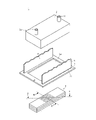
- FIG. 2 is an exploded perspective view showing an outline of an inkjet head according to a first embodiment of the present invention used in the image forming apparatus shown in FIG.
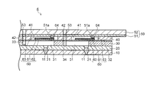
- FIG. 3 is a cross-sectional view taken along the line AA in FIG. 2 showing an outline of a head chip included in the inkjet head according to the first embodiment of the present invention.
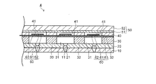
- FIG. 4 is a cross-sectional view taken along the line BB in FIG. 2 showing an outline of a head chip included in the inkjet head according to the first embodiment of the present invention.
- FIG. 1 is a schematic diagram showing the configuration of an image forming apparatus by an inkjet method.
- FIG. 2 is an exploded perspective view showing an outline of an inkjet head according to a first embodiment of the present invention used in the image forming apparatus shown in FIG.
- FIG. 3 is a cross-sectional view taken along the line AA in FIG. 2 showing an outline
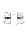
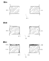
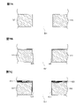
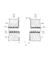
- FIG. 5 is a schematic partial cross section showing a state in which one flow path member containing single crystal silicon and another flow path member are bonded by an adhesive layer in the inkjet head according to the first embodiment of the present invention. It is a figure. 6A to 6C are first process diagrams showing a process of manufacturing an inkjet head according to the first embodiment of the present invention. 7A to 7C are second process diagrams showing a process of manufacturing an inkjet head according to the first embodiment of the present invention.
- FIG. 8 is a third process diagram showing a process of manufacturing an inkjet head according to the first embodiment of the present invention.
- the image forming apparatus according to the first embodiment of the present invention can be configured in the same manner as a known image forming apparatus by an inkjet method except that it has an inkjet head according to the present embodiment described later.
- the image forming apparatus 100 includes an inkjet head 1, an ink supply apparatus 120, a conveying apparatus 130, and a main tank 140.
- the inkjet head 1 has a plurality of nozzles for ejecting ink droplets onto a recording medium 150 such as paper which is a printed matter.
- the inkjet head 1 is configured to supply a plurality of types of inks having different colors to specific nozzles.
- the inkjet head 1 is arranged so as to be scannable in a direction crossing the transport direction X of the recording medium 150 on which an image is to be formed, for example.
- the configuration of the inkjet head 1 will be described later.
- the transport device 130 is a device for transporting the recording medium 150 to the inkjet head 1.
- the transport device 130 includes, for example, a belt conveyor 131 and a rotatable feed roller 132.
- the belt conveyor 131 is composed of rotatable pulleys 133a and 133b and endless belts 134 stretched on these pulleys 133a and 133b.
- the feed roller 132 is arranged at a position facing the pulley 133a on the upstream side in the transport direction X of the recording medium 150 so as to sandwich the belt 134 and the recording medium 150 and feed the recording medium 150 onto the belt 134.
- the ink supply device 120 is integrally arranged with the inkjet head 1.
- the ink supply device 120 is arranged for each type of ink. For example, when using four color inks of Y (yellow), M (magenta), C (cyan), and K (black), four ink supply devices 120 are arranged on the inkjet head 1.
- Each ink supply device 120 supplies ink in the main tank 140 via a tube 161 and a valve 164 connected to the main tank 140. Further, each ink supply device 120 communicates with the common ink chamber 2 described later of the inkjet head 1 via a tube 162, and is connected so that ink of each color can be supplied to the ink supply port 2a of the desired common ink chamber 2. There is.
- the inkjet head 1 is also connected to the main tank 140 by a bypass tube 163 branching from the above tube 161.
- a valve 164 that can switch and set the ink flow path is arranged in one or both of the pipe 161 and the bypass pipe 163.
- the tube 161 and the tube 162, and the bypass tube 163 are, for example, all flexible tubes.
- the valve 164 is, for example, a three-way valve.
- the main tank 140 is a tank for accommodating ink to be supplied to the inkjet head 1.
- the main tank 140 is arranged separately from the inkjet head 1.
- the main tank 140 has, for example, a stirring device (not shown).
- the main tank 140 can be appropriately determined according to the image forming performance, the size, and the like of the image forming apparatus 100.
- FIG. 2 is an exploded perspective view showing an outline of the inkjet head 1 used in the above-mentioned image forming apparatus 100.
- the inkjet head 1 has a common ink chamber 2, a holding portion 3, a head chip 4, and a flexible wiring board 5.
- the common ink chamber 2 is formed in a hollow substantially rectangular parallelepiped shape, and one surface facing the holding portion 3 is open.
- An ink supply port 2a for supplying ink from the ink supply device 120 and an ink discharge port 2b for discharging ink to the ink supply device 120 are provided on one surface of the common ink chamber 2 facing the opening.
- the common ink chamber 2 is provided with a filter inside, removes foreign matter from the ink supplied from the ink supply port 2a by the filter, and finely crushes air bubbles contained in the ink.
- the holding portion 3 is formed in a substantially flat plate shape having an opening 3a at a substantially center, and is arranged so as to cover the opening of the common ink chamber 2.
- the common ink chamber 2 is connected to one surface of the holding portion 3 so as to cover the opening 3a.
- the head tip 4 is connected to the other surface of the holding portion 3 so as to cover the opening 3a.
- the holding portion 3 communicates the common ink chamber 2 with the head chip 4 via the opening 3a.
- An insertion hole 3b is provided on the outer peripheral portion of the holding portion 3.
- the flexible wiring board 5 is inserted through the insertion hole 3b.
- One end of the flexible wiring board 5 is connected to the wiring board 50 of the head chip 4, which will be described later. Further, the other end of the flexible wiring board 5 is drawn out to the common ink chamber 2 side by inserting the insertion hole 3b provided in the holding portion 3 from the other surface of the holding portion 3.
- FIG. 3 is a cross-sectional view taken along the line AA in FIG. 2 showing an outline of the head chip 4 included in the above-mentioned inkjet head 1
- FIG. 4 is an outline of the head chip 4 included in the above-mentioned inkjet head 1. It is sectional drawing along the line BB in FIG.
- the head tip 4 has a nozzle plate 10, an intermediate plate 20, a pressure chamber forming plate 30, a drive plate 40, and a wiring board 50. Further, the head chip 4 is laminated in the order of the nozzle plate 10, the intermediate plate 20, the pressure chamber forming plate 30, the drive plate 40, and the wiring board 50 from the ink ejection surface side.
- a plurality of nozzle holes 11 are formed in the nozzle plate 10.
- the nozzle hole 11 penetrates from one surface to the other surface of the nozzle plate 10.
- the nozzle hole 11 has a cross-sectional shape narrowed so that the tip side of the ejection port has a small diameter, and the ink supplied from the common ink chamber 2 is ejected from the ejection port to the outside.
- a plurality of nozzle holes 11 are provided in the nozzle plate 10 and are arranged in a matrix.
- the nozzle hole 11 communicates with the pressure chamber 31 formed in the pressure chamber forming plate 30 via the intermediate plate 20 laminated on the nozzle plate 10.
- the intermediate plate 20 is arranged between the nozzle plate 10 and the pressure chamber forming plate 30.
- the intermediate plate 20 is provided with a first communication hole 21 for communicating the nozzle hole 11 and the pressure chamber 31 provided in the pressure chamber forming plate 30 described later.
- the first communication hole 21 is provided at a position corresponding to the nozzle hole 11 of the nozzle plate 10, and penetrates from one surface to the other surface of the intermediate plate 20.
- the pressure chamber forming plate 30 has a plurality of pressure chambers 31 and a diaphragm 32.
- the pressure chamber 31 is provided at a position corresponding to the nozzle hole 11 of the nozzle plate 10 and the first communication hole 21 of the intermediate plate 20. Further, the pressure chamber 31 penetrates from one surface to the other surface of the pressure chamber forming plate 30.
- the pressure chamber 31 applies ejection pressure to the ink ejected from the nozzle hole 11 due to its volume fluctuation. Further, the pressure chamber 31 is provided at a position corresponding to the nozzle hole 11 of the nozzle plate 10 and the first communication hole 21 of the intermediate plate 20.
- the diaphragm 32 is arranged so as to cover the opening on the opposite side of the intermediate plate 20 in the pressure chamber 31.
- the diaphragm 32 is provided with a second communication hole 33 that communicates with the pressure chamber 31.
- a drive plate 40 is arranged on one surface of the diaphragm 32 on the side opposite to the one on the pressure chamber 31 side.
- the drive plate 40 has a space portion 41 and a third communication hole 42 that communicates with the second communication hole 33.
- the space portion 41 is arranged at a position facing the pressure chamber 31 with the diaphragm 32 interposed therebetween.
- the actuator 60 is housed in the space portion 41.
- the actuator 60 has a piezoelectric element 61, a first electrode 62, and a second electrode 63.
- the first electrode 62 is laminated on one surface of the diaphragm 32.
- An insulating layer may be arranged between the first electrode 62 and the diaphragm 32.
- the piezoelectric element 61 is laminated on the first electrode 62, and is arranged for each pressure chamber 31 (each channel) at a position facing the pressure chamber 31 with the diaphragm 32 and the first electrode 62 sandwiched between them.
- the piezoelectric element 61 is made of a material that is deformed by applying a voltage, and is made of a ferroelectric material such as lead zirconate titanate (PZT), for example. Further, the second electrode 63 is laminated on the surface of the piezoelectric element 61 opposite to the first electrode 62. The second electrode 63 is connected to the wiring layer 51 provided on the wiring board 50, which will be described later, via the bump 64.
- PZT lead zirconate titanate
- the wiring board 50 has a wiring layer 51 and a silicon layer 52 in which the wiring layer 51 is formed on one surface.
- the wiring layer 51 is connected to the bump 64 provided on the second electrode 63 via the solder 51a. Further, the outer edge portion of the wiring layer 51 is connected to the flexible wiring board 5. Further, a silicon layer 52 is arranged on one surface of the wiring layer 51 on the opposite side of the drive plate 40. The silicon layer 52 is joined to the holding portion 3.
- the wiring board 50 is provided with a fourth communication hole 53 that penetrates the wiring layer 51 and the silicon layer 52.
- the fourth communication hole 53 communicates with the common ink chamber 2 via the third communication hole 42 of the drive plate 40 and the opening 3a of the holding portion 3.
- the ink in the common ink chamber 2 is pressed by the fourth communication hole 53 of the wiring board 50, the third communication hole 42 of the drive plate 40, and the second communication hole 33 of the diaphragm 32 that are communicated with each other.
- An inlet that serves as a flow path for supplying the chamber 31 is configured. The inlet plays a role of reducing the flow path resistance (flow rate) of the ink flowing from the common ink chamber 2 to the pressure chamber 31.
- the first communication hole 21 of the intermediate plate 20 and the nozzle hole 11 of the nozzle plate 10 that communicate with each other form an outlet for ejecting the ink in the pressure chamber 31 toward the recording medium 150.
- the ink contained in the common ink chamber 2 passes through the inlet (that is, the fourth communication hole 53, the third communication hole 42, and the second communication hole 33), and the pressure chamber 31 Flow into. Then, when a voltage is applied between the first electrode 62 and the second electrode 63, the piezoelectric element 61 operates and deforms (vibrates), and the vibrating plate 32 deforms (vibrates) as the piezoelectric element 61 deforms. Vibrate. When the diaphragm 32 is deformed (vibrated), pressure for ejecting ink into the pressure chamber 31 is generated.
- the ink in the pressure chamber 31 is pushed out to the outlet (that is, the first communication hole 21 and the nozzle hole 11), and is ejected from the tip of the nozzle hole 11 (nozzle opening) toward the recording medium 150. ..
- a plurality of flow path members (nozzle plate 10, intermediate plate 20, pressure chamber forming plate 30, drive plate 40, and wiring substrate 50) in which pores and grooves are formed by microfabrication are all formed. Are aligned and adhered to form the inkjet head 1. Then, the ink flow path (4th communication hole 53, 3rd communication hole 42, 2nd communication hole 33, pressure chamber 31, 1st communication hole 21 and nozzle hole 11) is formed by the above alignment.
- these flow path members is not particularly limited, and known materials such as silicon (Si), nickel (Ni), and stainless steel can be used.
- at least one flow path member is formed by processing a single crystal silicon wafer.
- these flow path members have a flow path member containing at least one single crystal silicon.
- the other flow path member may be a flow path member containing a material other than single crystal silicon, and is different from the above-mentioned one flow path member among a plurality of flow path members containing single crystal silicon. It may be another flow path member.
- FIG. 5 is a schematic partial cross-sectional view showing a state in which one flow path member containing single crystal silicon and another flow path member are joined by an adhesive layer.
- FIG. 5 shows a state in which the nozzle plate 10 as one flow path member containing single crystal silicon and the intermediate plate 20 as another flow path member are joined by the adhesive layer 70.
- the present embodiment is not limited to this, and may be a joint between other flow path members.
- the nozzle hole 11 formed in the nozzle plate 10 and the first communication hole 21 formed in the intermediate plate 20 are both inclined (diameters change along the ink flow direction). ) Although it is a through hole, the inclination of the through hole is omitted in FIG. 5 for the sake of preparation of explanation.
- both the nozzle plate 10 and the intermediate plate 20 are flow path members containing single crystal silicon formed by processing a silicon wafer.
- a protective film 15 is formed on the surface of the nozzle plate 10, and a protective film 25 is formed on the surface of the intermediate plate 20.
- the protective film 15 and the protective film 25 are protective films for increasing the resistance of these flow path members (nozzle plate 10 and intermediate plate 20) to ink.
- protective films may be formed on the surface of the flow path member (nozzle plate 10 and intermediate plate 20 in this embodiment) in contact with the ink flow path. However, it is preferable that it is also formed on a surface facing another flow path member. When these protective films are formed on the surface facing the other flow path member, the protective film 18 containing no silicon oxide is bonded to the protective film 18 containing no silicon oxide. It can be joined more firmly.
- protective film 15 and protective film 25 in this embodiment is not particularly limited, and the passivation-forming tantalum (Ta), zirconium (Zr), titanium (Ti), hafnium (Hf) and Oxides such as niobium (Nb), metal silicates containing silicon, intermetallic compounds containing chromium (Cr), nickel (Ni) and aluminum (Al), and polyimides, polyamides and parylenes.
- Organic materials such as can be used.
- the protective film preferably contains a compound containing a silicon oxide.
- the compound containing a silicon oxide include SiO 2 , SiOC, SiON, TaSiO, ZrSiO, TiSiO, and the like.
- the film thickness of these protective films is not particularly limited, but is preferably 20 nm or more and 1000 nm or less, and more preferably 30 nm or more and 500 nm or less.
- the film thickness is 30 nm or more, defects during film formation are likely to be suppressed, and the ink resistance of the flow path member is likely to be sufficiently increased.
- the film thickness is 500 nm or less, it is easy to prevent peeling and cracking due to stress of the thin film during manufacturing.
- the protective film is formed on both one member and the other members (nozzle plate 10 and intermediate plate 20), but the protective film is formed only on one of these flow path members.
- the protective film may not be formed on any of the flow path members.
- the protective film may be formed on either the one member or the other member, but at least one containing single crystal silicon. It is preferable that the protective film is formed on the member.
- the type of the adhesive constituting the adhesive layer 70 is not particularly limited, and a known adhesive such as an epoxy-based adhesive can be used. Since the epoxy-based adhesive forms a dense crosslinked structure with the curing agent, it is difficult for the ink to penetrate into the adhesive layer. Therefore, peeling of the flow path member due to the adhesive layer formed by the permeated ink is unlikely to occur.
- the layer thickness of the adhesive layer 70 is not particularly limited, but is preferably 0.3 ⁇ m or more and 10 ⁇ m or less, and more preferably 0.5 ⁇ m or more and 7 ⁇ m or less.
- the film thickness is 5 ⁇ m or more
- the flow path members can be more firmly bonded to each other.
- the adhesive layer can absorb foreign matter remaining on the surface of the flow path member (or the surface of the protective film) during manufacturing, so that the flow path member and the adhesive The bonding strength with the layer can be further increased.
- the layer thickness is 7 ⁇ m or less, it is possible to suppress the generation of foreign substances due to the overflow of the material of the adhesive layer during manufacturing, and also to prevent the outflow to unnecessary regions other than the adhesive region. Can be done.
- the adhesive layer 70 and a spacer ball for controlling the film thickness may be included.
- a protective film 18 containing no silicon oxide is arranged between the nozzle plate 10 and the adhesive layer 70.
- the protective film 18 containing no silicon oxide is in contact with both the protective film 15 and the adhesive layer 70 of the nozzle plate 10, and by joining with these, the nozzle plate 10 and the adhesive layer 70 are formed. And are joined.
- a protective film 28 containing no silicon oxide is arranged between the intermediate plate 20 and the adhesive layer 70.
- the protective film 28 containing no silicon oxide is in contact with both the protective film 25 and the adhesive layer 70 of the intermediate plate 20, and by joining with these, the intermediate plate 20 and the adhesive layer 70 are in contact with each other. And are joined.
- a step portion 75 due to a positional deviation at the time of joining these flow path members and a minute error at the time of formation is likely to occur at the joint portion between the flow path members.
- the stepped portion 75 tends to retain ink.
- minute gaps are likely to occur at the bonding interface between the flow path members, and ink that has entered the minute gaps is likely to stay. Therefore, it can be said that the joint portion between the flow path members is a portion where the influence of corrosion by the ink is likely to occur.
- the inks are alkaline in order to disperse pigments, but single crystal silicon and silicon oxides are easily corroded by alkalis.
- the flow path member made of single crystal silicon or the protective film containing silicon oxide is corroded by the ink, the ink enters and stays in the gap generated by the corrosion, so that the flow path member and the protective film are corroded. It will go further. Corrosion that occurs at the joint can cause peeling of the adhered flow path member.
- these protective films swell and the bonding strength between these protective films and the adhesive layer is weakened. The swelling can also cause peeling of the adhered flow path member.
- the protective film 18 that does not contain silicon oxide and the protective film 28 that does not contain silicon oxide are arranged at the joint portion where the ink is likely to stay. Compared with single crystal silicon and silicon oxide, these protective film 18 and protective film 28 are less likely to be corroded by alkali, and therefore swelling due to penetration of ink from the corrosion is less likely to occur.
- the flow path member nozzle plate 10 and intermediate plate 20 in this embodiment
- the adhesive layer 70 By joining the flow path member (nozzle plate 10 and intermediate plate 20 in this embodiment) and the adhesive layer 70 via the protective film 18 and the protective film 28 that are not easily corroded, peeling of the joint due to corrosion is less likely to occur. be able to.
- Examples of the materials of the protective film 18 and the protective film 28 include chromium (Cr), chromium oxide (Cr x Oy : CrO, Cr 2 O 3 and the like), titanium (Ta), and titanium oxide (Ta x Oy ). : Ta 2 O 5 and Ta O 2 etc.), Titanium (Ti), Titanium Oxide (TIO 2 ), Silicon Nitride (Si x N y : Si 3 N 4 etc.), Silicon Carbide (SiC) and the like.
- chromium, chromium oxide and silicon nitride are preferable from the viewpoint of further enhancing corrosion resistance
- TIO 2 is preferable from the viewpoint of further enhancing wettability.
- the film thicknesses of the protective film 18 and the protective film 28 are not particularly limited, but are preferably 20 nm or more and 1000 nm or less, and more preferably 30 nm or more and 500 nm or less.
- peeling of the joint due to corrosion can be more sufficiently suppressed, and defects during film formation can be easily suppressed.
- the film thickness is 30 nm or more, foreign matter remaining on the surface of the flow path member (or the surface of the protective film) at the time of manufacturing can be absorbed by the protective film 18 containing no silicon oxide.
- the bonding strength between the road member and the adhesive layer can be further increased.
- the film thickness is 500 nm or less, it is easy to prevent peeling and cracking due to stress of the thin film during manufacturing.
- the protective film 18 and the protective film 28 may be formed on the surface of the flow path member (nozzle plate 10 and intermediate plate 20 in this embodiment) facing the other flow path member, but the ink flow path may be formed. It may also be formed on the surface in contact with the surface. When the protective film 18 and the protective film 28 are formed on the surface in contact with the ink flow path, the wettability of the ink flow path to the ink can be improved.
- the protective film 18 and the protective film 28 are formed by various vapor deposition methods including physical vapor deposition (PVD) such as a sputtering method and chemical vapor deposition (CVD) such as an atomic layer deposition method (ALD). Can be done. Of these, chemical vapor deposition (CVD) such as atomic layer deposition (ALD), which has good coverage of complex shapes, is preferred.
- PVD physical vapor deposition
- CVD chemical vapor deposition
- ALD atomic layer deposition
- FIGS. 6 to 8 are explanatory views showing an example of a method for manufacturing an inkjet head according to the present embodiment.
- the scales of some members are changed for easy understanding.
- a first chip member 610 is prepared by microfabricating a silicon wafer and processing it into the shape of one flow path member (nozzle plate 10 in this embodiment).
- the first chip member 610 is formed with a large number of fine communication holes 611 by etching or the like.
- the communication hole 611 is a communication hole that becomes the nozzle hole 11 when the inkjet head is completed, and is processed into the same shape as the nozzle hole 11.
- a protective film 615 is formed on the first chip member 610 (a step of forming a protective film containing a compound containing a silicon oxide).
- the protective film 615 is a film member that becomes the protective film 15 when the inkjet head is completed, and is formed so as to have the thickness of the protective film 15 by the material (compound containing silicon oxide) described for the protective film 15.
- the method for forming the protective film 615 is not particularly limited, and is formed by various vapor deposition methods including physical vapor deposition (PVD) such as a sputtering method and chemical vapor deposition (CVD) such as an atomic layer deposition method (ALD). can do.
- PVD physical vapor deposition
- CVD chemical vapor deposition
- ALD atomic layer deposition
- the protective film 615 may be formed on the surface of the first chip member 610 that is in contact with the communication hole 611 that is the nozzle hole 11, but the surface that faces the other flow path member (the protective film 618 is formed). It is preferable to form it on the surface to be formed).
- a protective film 618 is formed on the first chip member 610 (a step of forming a protective film containing no silicon oxide in one flow path member).
- the protective film 618 is a film member that becomes a protective film 18 that does not contain silicon oxide when the inkjet head is completed.
- the protective film 18 that does not contain silicon oxide is made of the material described for the protective film 18 that does not contain silicon oxide. It is formed to have the thickness of.
- the method for forming the protective film 618 is not particularly limited, and is formed by various vapor deposition methods including physical vapor deposition (PVD) such as a sputtering method and chemical vapor deposition (CVD) such as an atomic layer deposition method (ALD). can do.
- PVD physical vapor deposition
- CVD chemical vapor deposition
- ALD atomic layer deposition
- the protective film 618 may be formed on the surface of the first chip member 610 that faces the other flow path member (intermediate plate 20), but is formed on the surface of the first chip member 610 that is in contact with the communication hole 611 that is the nozzle hole 11. May also be formed.
- the intermediate plate 20 is not always necessary, and the nozzle plate 10 and the pressure chamber forming plate 30 may be directly joined.
- a second chip member 620 is prepared by microfabricating the silicon wafer and processing it into the shape of another flow path member (intermediate plate 20 in this embodiment). ..
- the second chip member 620 is formed with a large number of fine communication holes 621 by etching or the like.
- the communication hole 621 is a communication hole that becomes the first communication hole 21 when the inkjet head is completed, and is processed into the same shape as the first communication hole 21.
- a protective film 625 is formed on the second chip member 620 (a step of forming a protective film containing a compound containing a silicon oxide).
- the protective film 625 is a film member that becomes the protective film 25 when the inkjet head is completed, and is formed so as to have the thickness of the protective film 25 by the material (compound containing silicon oxide) described for the protective film 25.
- the method for forming the protective film 625 is not particularly limited, and is formed by various vapor deposition methods including physical vapor deposition (PVD) such as a sputtering method and chemical vapor deposition (CVD) such as an atomic layer deposition method (ALD). can do.
- PVD physical vapor deposition
- CVD chemical vapor deposition
- ALD atomic layer deposition
- the protective film 625 may be formed on the surface of the second chip member 620 that is in contact with the communication hole 621 that is the first communication hole 21, but the surface that faces the other flow path member (protective film 628). It is preferable to form the surface on which the surface is formed.
- a protective film 628 is formed on the second chip member 620 (a step of forming a protective film containing no silicon oxide on other flow path members).
- the protective film 628 is a film member that becomes a protective film 28 that does not contain silicon oxide when the inkjet head is completed.
- the protective film 28 that does not contain silicon oxide is made of the material described for the protective film 28 that does not contain silicon oxide. It is formed to have the thickness of.
- the method for forming the protective film 628 is not particularly limited, and is formed by various vapor deposition methods including physical vapor deposition (PVD) such as a sputtering method and chemical vapor deposition (CVD) such as an atomic layer deposition method (ALD). can do.
- PVD physical vapor deposition
- CVD chemical vapor deposition
- ALD atomic layer deposition
- the adhesive 670 is applied to the surface of the first chip member on which the protective film 628 is formed.
- the adhesive 670 can be applied by a coating method such as bar coater, flexographic printing, or screen printing.
- the surface of the second chip member 620 on which the protective film 628 is formed (the second chip member 620 shown in FIG. 8 is an upside down version of the second chip member 620 shown in FIG. 7). Is aligned with the communication hole 611 and the communication hole 621, and then brought into contact with the adhesive 670 to pressurize. At this time, the adhesive 670 may be cured by heating as needed.
- the bonded body in which the first chip member 610 (nozzle plate 10) and the second chip member 620 (intermediate plate 20) are bonded by the adhesive layer 70 obtained by curing the adhesive 670 is formed. It can be obtained (see FIG. 5).
- the inkjet head 1 can be obtained by aligning and bonding the pressure chamber forming plate 30, the drive plate 40, and the wiring board 50 so that the ink flow paths communicate with each other.
- one channel member and the other channel member are both described as containing single crystal silicon, but only one of them may contain single crystal silicon. That is, one flow path member may contain single crystal silicon, and the other flow path member may be made of another material.
- the protective film containing no silicon oxide may be arranged between the flow path member containing single crystal silicon and the adhesive layer, but the flow path member containing single crystal silicon and the adhesive layer may be arranged. It may be placed in between.
- one flow path member is a nozzle plate and the other flow path member is an intermediate plate.
- the other flow path members include single crystal silicon
- the flow is concerned.
- a protective film containing no silicon oxide may be arranged at the joint between the road member and the other flow path member.
- the nozzle plate and the intermediate plate may be formed of a material other than single crystal silicon.
- the protective film containing no silicon oxide may be arranged between one flow path member containing single crystal silicon and the adhesive layer, but does not come into contact with the adhesive layer of one flow path member.
- a protective film containing no silicon oxide may be formed on the surface.
- an adhesive is applied to one flow path member containing single crystal silicon to be bonded to the other flow path member, but an adhesive is applied to the other flow path member. It may be bonded to one flow path member containing single crystal silicon.
- the inkjet head ejects water-based ink, in order to eject other types of ink such as solvent-based ink, active ray-curable ink, and hot melt ink, the above-mentioned embodiment is described. Inkjet heads may be used.
- the inkjet head of the present invention peeling of the adhered flow path member is unlikely to occur. Therefore, according to the inkjet head of the present invention, the durability of the inkjet head can be further improved, and it is expected to contribute to the further spread of the inkjet head.
Landscapes
- Particle Formation And Scattering Control In Inkjet Printers (AREA)
Priority Applications (2)
| Application Number | Priority Date | Filing Date | Title |
|---|---|---|---|
| PCT/JP2020/037226 WO2022070334A1 (ja) | 2020-09-30 | 2020-09-30 | インクジェットヘッドおよびその製造方法、ならびに画像形成装置 |
| JP2022553328A JP7552708B2 (ja) | 2020-09-30 | 2020-09-30 | インクジェットヘッドおよびその製造方法、ならびに画像形成装置 |
Applications Claiming Priority (1)
| Application Number | Priority Date | Filing Date | Title |
|---|---|---|---|
| PCT/JP2020/037226 WO2022070334A1 (ja) | 2020-09-30 | 2020-09-30 | インクジェットヘッドおよびその製造方法、ならびに画像形成装置 |
Publications (1)
| Publication Number | Publication Date |
|---|---|
| WO2022070334A1 true WO2022070334A1 (ja) | 2022-04-07 |
Family
ID=80949986
Family Applications (1)
| Application Number | Title | Priority Date | Filing Date |
|---|---|---|---|
| PCT/JP2020/037226 Ceased WO2022070334A1 (ja) | 2020-09-30 | 2020-09-30 | インクジェットヘッドおよびその製造方法、ならびに画像形成装置 |
Country Status (2)
| Country | Link |
|---|---|
| JP (1) | JP7552708B2 (cg-RX-API-DMAC7.html) |
| WO (1) | WO2022070334A1 (cg-RX-API-DMAC7.html) |
Cited By (1)
| Publication number | Priority date | Publication date | Assignee | Title |
|---|---|---|---|---|
| JPWO2025258499A1 (cg-RX-API-DMAC7.html) * | 2024-06-11 | 2025-12-18 |
Citations (5)
| Publication number | Priority date | Publication date | Assignee | Title |
|---|---|---|---|---|
| JP2006218716A (ja) * | 2005-02-10 | 2006-08-24 | Seiko Epson Corp | 液体噴射ヘッド及び液体噴射装置 |
| JP2007245589A (ja) * | 2006-03-16 | 2007-09-27 | Seiko Epson Corp | 液体噴射ヘッド及び液体噴射装置 |
| US20100182375A1 (en) * | 2006-10-17 | 2010-07-22 | Telecom Italia S.P.A. | Ink jet printing head |
| JP2014124882A (ja) * | 2012-12-27 | 2014-07-07 | Seiko Epson Corp | 液体噴射ヘッド及び液体噴射装置 |
| JP2019214167A (ja) * | 2018-06-13 | 2019-12-19 | コニカミノルタ株式会社 | ノズルプレートの製造方法、インクジェットヘッドの製造方法、ノズルプレート及びインクジェットヘッド |
-
2020
- 2020-09-30 WO PCT/JP2020/037226 patent/WO2022070334A1/ja not_active Ceased
- 2020-09-30 JP JP2022553328A patent/JP7552708B2/ja active Active
Patent Citations (5)
| Publication number | Priority date | Publication date | Assignee | Title |
|---|---|---|---|---|
| JP2006218716A (ja) * | 2005-02-10 | 2006-08-24 | Seiko Epson Corp | 液体噴射ヘッド及び液体噴射装置 |
| JP2007245589A (ja) * | 2006-03-16 | 2007-09-27 | Seiko Epson Corp | 液体噴射ヘッド及び液体噴射装置 |
| US20100182375A1 (en) * | 2006-10-17 | 2010-07-22 | Telecom Italia S.P.A. | Ink jet printing head |
| JP2014124882A (ja) * | 2012-12-27 | 2014-07-07 | Seiko Epson Corp | 液体噴射ヘッド及び液体噴射装置 |
| JP2019214167A (ja) * | 2018-06-13 | 2019-12-19 | コニカミノルタ株式会社 | ノズルプレートの製造方法、インクジェットヘッドの製造方法、ノズルプレート及びインクジェットヘッド |
Cited By (2)
| Publication number | Priority date | Publication date | Assignee | Title |
|---|---|---|---|---|
| JPWO2025258499A1 (cg-RX-API-DMAC7.html) * | 2024-06-11 | 2025-12-18 | ||
| WO2025258499A1 (ja) * | 2024-06-11 | 2025-12-18 | コニカミノルタ株式会社 | 圧電アクチュエーター、インクジェットヘッド、及びインクジェット記録装置 |
Also Published As
| Publication number | Publication date |
|---|---|
| JP7552708B2 (ja) | 2024-09-18 |
| JPWO2022070334A1 (cg-RX-API-DMAC7.html) | 2022-04-07 |
Similar Documents
| Publication | Publication Date | Title |
|---|---|---|
| US20120320131A1 (en) | Inkjet head and inkjet recording device | |
| CN101415560B (zh) | 液体喷出装置 | |
| JP2006096034A (ja) | 溝付き振動板及び圧電層を有する圧電アクチュエータ、液体移送装置及びその製造方法 | |
| CN101254696A (zh) | 液体喷射头组件的制造方法以及液体喷射头组件 | |
| JP2006334910A (ja) | インクジェットヘッド | |
| JP7552708B2 (ja) | インクジェットヘッドおよびその製造方法、ならびに画像形成装置 | |
| US7445318B2 (en) | Method of manufacturing liquid droplet ejection head, liquid droplet ejection head, and liquid droplet ejection apparatus | |
| JP4508595B2 (ja) | 液体噴射ヘッド及びその製造方法並びに液体噴射装置 | |
| CN108602350A (zh) | 喷嘴构件和使用该喷嘴构件的液体排出头以及记录装置 | |
| US7914127B2 (en) | Nozzle plate for an ink jet print head comprising stress relieving elements | |
| JP6025052B2 (ja) | 液滴吐出ヘッド及び画像形成装置 | |
| JP2012061689A (ja) | 液滴吐出ヘッド、液滴吐出ヘッドの製造方法、液体カートリッジ及び画像形成装置 | |
| JP2011018836A (ja) | 圧電型アクチュエータの製造方法、及び該製造方法によって製造された圧電型アクチュエータ | |
| JP2023073667A (ja) | ヘッドチップ、液体噴射ヘッド、液体噴射記録装置及びヘッドチップの製造方法 | |
| JP2009178893A (ja) | 液体移送装置及び液体移送装置の製造方法 | |
| JP2013158991A (ja) | 液滴吐出ヘッド、インクカートリッジおよび画像形成装置 | |
| JP5338585B2 (ja) | 液体吐出ヘッド及び画像形成装置 | |
| JP2019155590A (ja) | インクジェットヘッド、インクジェット記録装置及びインクジェットヘッドの製造方法 | |
| JP7047587B2 (ja) | インクジェットヘッドおよびインクジェット画像形成装置 | |
| JP2013163341A (ja) | 液滴吐出ヘッド、インクカートリッジおよび画像形成装置 | |
| JP2011037055A (ja) | 液体噴射ヘッドの製造方法、液体噴射ヘッド及び液体噴射装置 | |
| JP2015058583A (ja) | 液滴吐出ヘッド及び画像形成装置 | |
| JP5896275B2 (ja) | 液滴吐出ヘッド及び画像形成装置 | |
| JP7193334B2 (ja) | ヘッドチップ、液体噴射ヘッド、液体噴射記録装置およびヘッドチップの製造方法 | |
| JP7820694B2 (ja) | 液体噴射ヘッド及び液体噴射装置 |
Legal Events
| Date | Code | Title | Description |
|---|---|---|---|
| 121 | Ep: the epo has been informed by wipo that ep was designated in this application |
Ref document number: 20956262 Country of ref document: EP Kind code of ref document: A1 |
|
| ENP | Entry into the national phase |
Ref document number: 2022553328 Country of ref document: JP Kind code of ref document: A |
|
| NENP | Non-entry into the national phase |
Ref country code: DE |
|
| 122 | Ep: pct application non-entry in european phase |
Ref document number: 20956262 Country of ref document: EP Kind code of ref document: A1 |