WO2022059488A1 - 窒化物半導体ウェーハの製造方法 - Google Patents
窒化物半導体ウェーハの製造方法 Download PDFInfo
- Publication number
- WO2022059488A1 WO2022059488A1 PCT/JP2021/032147 JP2021032147W WO2022059488A1 WO 2022059488 A1 WO2022059488 A1 WO 2022059488A1 JP 2021032147 W JP2021032147 W JP 2021032147W WO 2022059488 A1 WO2022059488 A1 WO 2022059488A1
- Authority
- WO
- WIPO (PCT)
- Prior art keywords
- nitride semiconductor
- single crystal
- silicon single
- crystal substrate
- semiconductor wafer
- Prior art date
- Legal status (The legal status is an assumption and is not a legal conclusion. Google has not performed a legal analysis and makes no representation as to the accuracy of the status listed.)
- Ceased
Links
Images



Classifications
-
- H—ELECTRICITY
- H10—SEMICONDUCTOR DEVICES; ELECTRIC SOLID-STATE DEVICES NOT OTHERWISE PROVIDED FOR
- H10P—GENERIC PROCESSES OR APPARATUS FOR THE MANUFACTURE OR TREATMENT OF DEVICES COVERED BY CLASS H10
- H10P14/00—Formation of materials, e.g. in the shape of layers or pillars
- H10P14/20—Formation of materials, e.g. in the shape of layers or pillars of semiconductor materials
- H10P14/29—Formation of materials, e.g. in the shape of layers or pillars of semiconductor materials characterised by the substrates
- H10P14/2901—Materials
- H10P14/2902—Materials being Group IVA materials
- H10P14/2905—Silicon, silicon germanium or germanium
-
- H—ELECTRICITY
- H10—SEMICONDUCTOR DEVICES; ELECTRIC SOLID-STATE DEVICES NOT OTHERWISE PROVIDED FOR
- H10P—GENERIC PROCESSES OR APPARATUS FOR THE MANUFACTURE OR TREATMENT OF DEVICES COVERED BY CLASS H10
- H10P14/00—Formation of materials, e.g. in the shape of layers or pillars
- H10P14/20—Formation of materials, e.g. in the shape of layers or pillars of semiconductor materials
- H10P14/32—Formation of materials, e.g. in the shape of layers or pillars of semiconductor materials characterised by intermediate layers between substrates and deposited layers
- H10P14/3202—Materials thereof
- H10P14/3214—Materials thereof being Group IIIA-VA semiconductors
- H10P14/3216—Nitrides
-
- H—ELECTRICITY
- H10—SEMICONDUCTOR DEVICES; ELECTRIC SOLID-STATE DEVICES NOT OTHERWISE PROVIDED FOR
- H10P—GENERIC PROCESSES OR APPARATUS FOR THE MANUFACTURE OR TREATMENT OF DEVICES COVERED BY CLASS H10
- H10P14/00—Formation of materials, e.g. in the shape of layers or pillars
- H10P14/20—Formation of materials, e.g. in the shape of layers or pillars of semiconductor materials
- H10P14/32—Formation of materials, e.g. in the shape of layers or pillars of semiconductor materials characterised by intermediate layers between substrates and deposited layers
- H10P14/3242—Structure
- H10P14/3244—Layer structure
- H10P14/3251—Layer structure consisting of three or more layers
-
- H—ELECTRICITY
- H10—SEMICONDUCTOR DEVICES; ELECTRIC SOLID-STATE DEVICES NOT OTHERWISE PROVIDED FOR
- H10P—GENERIC PROCESSES OR APPARATUS FOR THE MANUFACTURE OR TREATMENT OF DEVICES COVERED BY CLASS H10
- H10P14/00—Formation of materials, e.g. in the shape of layers or pillars
- H10P14/20—Formation of materials, e.g. in the shape of layers or pillars of semiconductor materials
- H10P14/34—Deposited materials, e.g. layers
- H10P14/3402—Deposited materials, e.g. layers characterised by the chemical composition
- H10P14/3414—Deposited materials, e.g. layers characterised by the chemical composition being group IIIA-VIA materials
- H10P14/3416—Nitrides
-
- H—ELECTRICITY
- H10—SEMICONDUCTOR DEVICES; ELECTRIC SOLID-STATE DEVICES NOT OTHERWISE PROVIDED FOR
- H10P—GENERIC PROCESSES OR APPARATUS FOR THE MANUFACTURE OR TREATMENT OF DEVICES COVERED BY CLASS H10
- H10P14/00—Formation of materials, e.g. in the shape of layers or pillars
- H10P14/20—Formation of materials, e.g. in the shape of layers or pillars of semiconductor materials
- H10P14/36—Formation of materials, e.g. in the shape of layers or pillars of semiconductor materials characterised by treatments done before the formation of the materials
-
- H—ELECTRICITY
- H10—SEMICONDUCTOR DEVICES; ELECTRIC SOLID-STATE DEVICES NOT OTHERWISE PROVIDED FOR
- H10P—GENERIC PROCESSES OR APPARATUS FOR THE MANUFACTURE OR TREATMENT OF DEVICES COVERED BY CLASS H10
- H10P14/00—Formation of materials, e.g. in the shape of layers or pillars
- H10P14/20—Formation of materials, e.g. in the shape of layers or pillars of semiconductor materials
- H10P14/38—Formation of materials, e.g. in the shape of layers or pillars of semiconductor materials characterised by treatments done after the formation of the materials
-
- H—ELECTRICITY
- H10—SEMICONDUCTOR DEVICES; ELECTRIC SOLID-STATE DEVICES NOT OTHERWISE PROVIDED FOR
- H10P—GENERIC PROCESSES OR APPARATUS FOR THE MANUFACTURE OR TREATMENT OF DEVICES COVERED BY CLASS H10
- H10P36/00—Gettering within semiconductor bodies
Definitions
- the present invention relates to a method for manufacturing a nitride semiconductor wafer.
- CMOS complementary metal-oxide-semiconductor
- III-V semiconductors III-V semiconductors
- nitride semiconductors III-V semiconductors
- filters using piezoelectric materials A silicon single crystal substrate on which inexpensive and large-diameter wafers are distributed is suitable as a substrate as a base for these devices.
- the harmonic is a high-order frequency component that is an integral multiple of the original frequency.
- the original frequency is the fundamental wave
- the one with twice the frequency (1/2 wavelength) of the fundamental wave is the second harmonic
- the one with three times the frequency (one third wavelength) of the fundamental wave is the third harmonic.
- a substrate with small harmonics is required to avoid interference due to harmonics.
- Patent Document 1 describes switching characteristics by irradiating a wide-gap bipolar semiconductor for power use with one of ⁇ -rays, electron beams, and charged particle beams in advance to adjust the carrier life within a predetermined range. However, there is no mention of deterioration of the second and third harmonic characteristics.
- the present invention has been made to solve the above problems, and to improve and improve the second and third harmonic characteristics in a nitride semiconductor wafer in which a nitride semiconductor film is formed on a silicon single crystal substrate.
- An object of the present invention is to provide a method for manufacturing a nitride semiconductor wafer in which deterioration of characteristics is suppressed.
- the present invention has been made to achieve the above object, and is a method for manufacturing a nitride semiconductor wafer in which a nitride semiconductor film is formed on a silicon single crystal substrate, wherein the silicon single crystal substrate has a resistance.
- a nitride semiconductor wafer including a step of forming the nitride semiconductor film on the silicon single crystal substrate and a step of irradiating the silicon single crystal substrate with an electron beam using a wafer having a ratio of 100 ⁇ cm or more. Provides a manufacturing method for.
- a method for manufacturing a nitride semiconductor wafer by irradiating a silicon single crystal substrate having a resistivity of 100 ⁇ cm or more with an electron beam, the second and third harmonic characteristics are improved and improved, and the characteristics are deteriorated. It is possible to manufacture a nitride semiconductor wafer in which the amount of wafer is suppressed.
- the step of irradiating the electron beam can be performed before the step of forming the nitride semiconductor film.
- the step of irradiating the electron beam can be performed after the step of forming the nitride semiconductor film.
- the electron beam can be irradiated before or after the step of forming the nitride semiconductor film.
- the second in a nitride semiconductor wafer in which a nitride semiconductor film is formed on a silicon single crystal substrate as used for a high frequency device, the second. It is possible to improve and improve the third harmonic characteristic and suppress the deterioration of the characteristic.
- CPW Co-Planar Waveguide
- the present inventors are a method for manufacturing a nitride semiconductor wafer in which a nitride semiconductor film is formed on a silicon single crystal substrate, and the resistance of the silicon single crystal substrate is high.
- a nitride semiconductor wafer including a step of forming the nitride semiconductor film on the silicon single crystal substrate and a step of irradiating the silicon single crystal substrate with an electron beam using a wafer having a size of 100 ⁇ cm or more.
- the method for manufacturing the nitride semiconductor wafer of the present invention will be described with reference to FIG.
- the following structure of the nitride semiconductor wafer is an example, and is not limited thereto.
- a silicon single crystal substrate with a resistivity of 100 ⁇ cm or more As will be described using specific data in Examples and Comparative Examples described later, the present inventors have used a silicon single crystal substrate having a resistivity of 100 ⁇ cm or more to form an electron beam on the silicon single crystal substrate. It has been found that it is possible to improve the second and third harmonic characteristics when irradiated with (EB).
- the upper limit of the resistivity is not particularly limited, and the larger the resistivity is, the more suitable it is for the method for manufacturing a nitride semiconductor wafer according to the present invention. be able to.
- the silicon single crystal substrate is irradiated with an electron beam.
- the effect of inactivating carriers such as dopants and / or impurities derived from raw materials in the silicon single crystal substrate can be remarkably obtained.
- the inactivation here is that the irradiation of the electron beam causes the point defects to be formed in the silicon single crystal substrate, and these trap the carriers in the silicon single crystal substrate. Or it depends on the reaction of the carrier. Further, it is considered that the resistance changes due to the decrease in the mobility of the dopant and / or the carrier due to the point defect. As a result of inactivating the dopant and / or carrier in the silicon single crystal substrate, it is considered that the silicon single crystal substrate has a high resistivity. Further, when the electron beam is irradiated after forming the nitride semiconductor film, it is considered that, in addition to the above effects, the point defects in the nitride semiconductor film are reduced and the characteristics are improved.
- the irradiation conditions of the electron beam are not particularly limited, and for example, electrons having an energy of 250 keV or more can be used. When it is about 250 keV or more, point defects can be more reliably formed in the silicon single crystal substrate, and carriers such as dopants and / or raw material-derived impurities in the silicon single crystal substrate can be inactivated.
- the upper limit of irradiation energy is not particularly limited.
- the irradiation dose can be, for example, 1 ⁇ 10 13 / cm 2 or more and 1 ⁇ 10 16 / cm 2 or less.
- the irradiation amount can be, for example, 1 ⁇ 10 13 / cm 2 or more and 1 ⁇ 10 16 / cm 2 or less.
- a sufficient amount of point defects can be stably generated in the silicon single crystal substrate.
- the time required for irradiation does not become too long, which is efficient.
- 2MeV, 1 ⁇ 10 15 / cm 2 electron beam irradiation can be performed. Further, the electron beam may irradiate the entire surface of the silicon single crystal substrate surface.
- this electron beam irradiation can also be performed after the nitride semiconductor film is formed.
- electron beam irradiation may be performed between the formation of the plurality of nitride semiconductor layers.
- the electron beam irradiation is performed after the nitride semiconductor film is formed, it can be performed before or after the device is manufactured.
- a nitride semiconductor film is formed by epitaxial growth.
- the nitride semiconductor film to be formed is not particularly limited, and may be a single layer or a plurality of layers as long as it includes at least one nitride semiconductor layer.
- an intermediate layer can be formed first, and then a device layer can be formed.
- an AlN layer having a thickness of, for example, 150 nm is formed on a silicon single crystal substrate, an AlGaN layer having a thickness of, for example, 160 nm is formed on the AlN layer, and an AlGaN layer having a thickness of 160 nm is alternately formed on the AlGaN layer. It is possible to form a superlattice layer in which a set is laminated.
- a device layer that can be formed on the intermediate layer a GaN layer having a thickness of, for example, 800 nm is formed on the intermediate layer, an AlGaN layer having a thickness of, for example, 25 nm is formed on the intermediate layer, and then, for example, the thickness is further formed.
- a 3 nm GaN layer can be formed.
- a CPW (Co-Planar Waveguide) Al electrode as shown in FIG. 2 can be formed for measurement and evaluation of harmonic characteristics.
- a nitride semiconductor wafer produced by forming a nitride semiconductor film by epitaxial growth is taken out from a film forming apparatus, an insulating film is formed on the wafer, and a CPW Al electrode is formed on the insulating film by photolithography.
- CPW has a structure in which metal electrodes are arranged in parallel with a gap, and a linear central metal electrode is formed in parallel with these metal electrodes in the center of the gap.
- a linear gap is provided in the center of the metal electrode, and the linear electrode is formed in the center of the gap so as not to touch the outer metal electrode.
- CPW transmits electromagnetic waves by an electric field in the direction from the central metal electrode toward the metal electrodes on both the left and right sides and the inside of the semiconductor substrate, and a magnetic field in the direction surrounding the central metal electrode inside the semiconductor substrate. If CPW is formed on the wafer, the harmonic characteristics can be measured. Harmonic Distortion (HD) can be measured by using CPW.
- HD Harmonic Distortion
- the manufactured high-frequency device can improve and improve the second and third harmonic characteristics and suppress the deterioration of the characteristics. can.
- Example 2 Two types (100 ⁇ cm and 6000 ⁇ cm) of silicon single crystal substrates having different resistivitys were prepared.
- an AlN layer having a thickness of 150 nm is formed on the silicon single crystal substrate as shown in FIG. 1, and an AlGaN layer having a thickness of 160 nm is formed on the AlN layer.
- 70 sets of GaN layers and AlN layers were alternately laminated on the superlattice layer.
- a GaN layer having a thickness of 800 nm was formed, an AlGaN layer having a thickness of 25 nm was formed on the GaN layer, and a GaN layer having a thickness of 3 nm was further formed on the AlGaN layer.
- the nitride semiconductor wafer on which the nitride semiconductor film is formed by epitaxial growth is taken out from the film forming apparatus, an insulating film is formed on the wafer, and the CPW Al electrode (line length: 2199 ⁇ m) as shown in FIG. 2 is subjected to photolithography. Formed.
- the second harmonic characteristics (2HD) and the third harmonic characteristics (2HD) of each element of the nitride semiconductor wafer before the electron beam irradiation was measured.
- electron beam irradiation was performed.
- the electron beam irradiation (2MeV, 1 ⁇ 10 15 / cm 2 ) was performed by Nissin Electric Co., Ltd. (NHV Corporation 3000kV machine).
- the second harmonic characteristics (2HD) and the third harmonic characteristics (3HD) of each element of the nitride semiconductor wafer after electron beam irradiation were measured.
- Nitride semiconductor film is formed on the silicon single crystal substrate, CPW is formed, and electron beam is irradiated, except that two types (8 m ⁇ cm, 5 ⁇ cm) of silicon single crystal substrates having different resistivitys are prepared. Then, the harmonic characteristics were measured before and after the electron beam irradiation.
- FIG. 3 is a graph showing the second harmonic characteristics of the substrate of each resistivity.
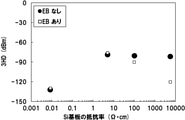
- FIG. 4 is a graph showing the third harmonic characteristics of the substrate of each resistivity. The larger the negative value on the vertical axis in these graphs, the better.
- FIGS. 3 and 4 in the nitride semiconductor wafer having a resistance of 10 ⁇ cm or less on the silicon single crystal substrate, the second and third harmonic characteristics did not change due to electron beam irradiation. In the nitride semiconductor wafer having a resistance of 100 ⁇ cm or more on the silicon single crystal substrate, improvement was observed in the second and third harmonic losses. As shown in FIG.
- the present invention is not limited to the above embodiment.
- the above-described embodiment is an example, and the present invention can be anything that has substantially the same configuration as the technical idea described in the claims of the present invention and exhibits the same function and effect. Is included in the technical scope of.
Landscapes
- Crystals, And After-Treatments Of Crystals (AREA)
Abstract
本発明は、シリコン単結晶基板の上に窒化物半導体膜を形成する窒化物半導体ウェーハの製造方法であって、前記シリコン単結晶基板として、抵抗率が100Ωcm以上であるのものを用いて、前記シリコン単結晶基板の上に前記窒化物半導体膜を形成する工程と、前記シリコン単結晶基板に電子線を照射する工程とを含む窒化物半導体ウェーハの製造方法である。これにより、シリコン単結晶基板上に窒化物半導体膜が形成された窒化物半導体ウェーハにおいて、第2・第3高調波特性を改善、向上し、特性劣化が抑制された窒化物半導体ウェーハの製造方法を提供する。
Description
本発明は、窒化物半導体ウェーハの製造方法に関する。
高周波デバイスの小型化、低コスト化に向けて、アンテナやアンプ、スイッチ、フィルター等のデバイスをインテグレーションする開発が進められている。また、周波数の高周波化に従い、回路が複雑化し、使用されるデバイスも、シリコンCMOS、III-V族半導体や窒化物半導体を用いたデバイス、圧電体を用いたフィルターなど多岐にわたっている。これらのデバイスの下地となる基板として、安価で大口径のウェーハが流通しているシリコン単結晶基板が適している。
しかし、上記のような高周波デバイスでは、基板起因の特性劣化、基板による損失及び第2・第3高調波特性劣化がみられる。
ここで、高調波とは、元となる周波数の整数倍の高次の周波数成分のことである。元の周波数を基本波とし、基本波の2倍の周波数(2分の1の波長)を持つものが第2高調波、基本波の3倍の周波数(3分の1の波長)を持つものが第3高調波と定義されている。高周波回路では、高調波による混信を避けるために高調波の小さい基板が必要とされる。
ここで、高調波とは、元となる周波数の整数倍の高次の周波数成分のことである。元の周波数を基本波とし、基本波の2倍の周波数(2分の1の波長)を持つものが第2高調波、基本波の3倍の周波数(3分の1の波長)を持つものが第3高調波と定義されている。高周波回路では、高調波による混信を避けるために高調波の小さい基板が必要とされる。
特許文献1には、パワー用途のワイドギャップバイポーラ半導体に、予めγ線、電子線、荷電粒子線の1つを照射して、キャリア寿命を所定の範囲になるように調整することで、スイッチング特性を向上させることが記載されているが、第2・第3高調波特性の劣化については言及されていない。
本発明は、上記問題を解決するためになされたものであり、シリコン単結晶基板上に窒化物半導体膜が形成された窒化物半導体ウェーハにおいて、第2・第3高調波特性を改善、向上し、特性劣化が抑制された窒化物半導体ウェーハの製造方法を提供することを目的とする。
本発明は、上記目的を達成するためになされたものであり、シリコン単結晶基板の上に窒化物半導体膜を形成する窒化物半導体ウェーハの製造方法であって、前記シリコン単結晶基板として、抵抗率が100Ωcm以上であるのものを用いて、前記シリコン単結晶基板の上に前記窒化物半導体膜を形成する工程と、前記シリコン単結晶基板に電子線を照射する工程とを含む窒化物半導体ウェーハの製造方法を提供する。
このような窒化物半導体ウェーハの製造方法によれば、抵抗率が100Ωcm以上のシリコン単結晶基板に電子線を照射することで、第2・第3高調波特性を改善、向上し、特性劣化が抑制された窒化物半導体ウェーハを製造することができる。
このとき、前記電子線を照射する工程を、前記窒化物半導体膜を形成する工程の前に行うことができる。
また、このとき、前記電子線を照射する工程を、前記窒化物半導体膜を形成する工程の後に行うことができる。
このように、シリコン単結晶基板に電子線を照射することができれば、電子線の照射は、窒化物半導体膜を形成する工程の前に行うこともできるし、後に行うこともできる。
以上のように、本発明に係る窒化物半導体ウェーハの製造方法によれば、高周波デバイスに用いるようなシリコン単結晶基板上に、窒化物半導体膜が形成された窒化物半導体ウェーハにおいて、第2・第3高調波特性を改善、向上し、特性劣化を抑制することが可能となる。
以下、本発明を詳細に説明するが、本発明はこれらに限定されるものではない。
上述のように、シリコン単結晶基板上に窒化物半導体膜が形成された窒化物半導体ウェーハにおいて、第2・第3高調波特性を改善、向上し、特性劣化が抑制された窒化物半導体ウェーハの製造方法が求められていた。
本発明者らは、上記課題について鋭意検討を重ねた結果、シリコン単結晶基板の上に窒化物半導体膜を形成する窒化物半導体ウェーハの製造方法であって、前記シリコン単結晶基板として、抵抗率が100Ωcm以上であるのものを用いて、前記シリコン単結晶基板の上に前記窒化物半導体膜を形成する工程と、前記シリコン単結晶基板に電子線を照射する工程とを含む窒化物半導体ウェーハの製造方法により、第2・第3高調波特性を改善、向上し、特性劣化が抑制された窒化物半導体ウェーハを製造することができることを見出し、本発明を完成した。
以下、図面を参照して説明する。
本発明の窒化物半導体ウェーハの製造方法について図1を用いて説明する。なお、以下の窒化物半導体ウェーハの構造は一例であって、これに限定されるものではない。
最初に、抵抗率が100Ωcm以上のシリコン単結晶基板を準備する。本発明者らは、後述の実施例、比較例で具体的なデータを用いて説明するように、シリコン単結晶基板として抵抗率が100Ωcm以上のものを用いることで、シリコン単結晶基板に電子線(EB)を照射したときに、第2・第3高調波特性を改善することが可能となることを見出した。抵抗率の上限は特に限定されず、抵抗率が大きいほど本発明に係る窒化物半導体ウェーハの製造方法に適しているが、基板の高抵抗率化は非常に難しいため、例えば10000Ωcmを上限とすることができる。
次に、このシリコン単結晶基板に電子線照射を行う。電子線を照射することで、シリコン単結晶基板中のドーパント及び/又は原料由来の不純物等のキャリアを不活性化させることによる効果が顕著に得られる。ここでの不活性化は、すなわち、電子線を照射することで、シリコン単結晶基板中に点欠陥が形成され、これらがシリコン単結晶基板中のキャリアをトラップするといった、点欠陥とドーパント及び/又はキャリアの反応による。また、点欠陥によってドーパント及び/又はキャリアの移動度が低下することで抵抗が変化すると考えられる。シリコン単結晶基板中のドーパント及び/又はキャリアを不活性化させた結果、シリコン単結晶基板が高抵抗率化すると考えられる。また、窒化物半導体膜を形成した後に電子線を照射する場合、上記効果に加え、窒化物半導体膜中の点欠陥が減少し、特性が向上するものと考えられる。
電子線の照射条件は特に限定されず、例えば、250keV以上のエネルギーをもつ電子を用いることができる。約250keV以上であれば、より確実にシリコン単結晶基板中に点欠陥を形成でき、シリコン単結晶基板中のドーパント及び/又は原料由来の不純物等のキャリアを不活性化させることができる。なお、照射エネルギーの上限は特に問わない。
照射線量は、例えば1×10¹³/cm2以上、1×1016/cm2以下とすることができる。照射量を1×1013/cm2以上とすることで、シリコン単結晶基板中に十分な量の点欠陥を安定して発生させることができる。また、照射量を1×1016/cm2以下とすることで、照射に要する時間が長くなりすぎることがないため、効率的である。例えば、2MeV、1×1015/cm2の電子線照射を行うことができる。また、電子線は、シリコン単結晶基板表面の全面に照射してもよい。なお、シリコン単結晶基板に電子線を照射することができれば、この電子線照射は窒化物半導体膜を形成した後に行うこともできる。窒化物半導体膜として複数層の窒化物半導体層を形成する場合には、複数層の窒化物半導体層の形成の間に電子線照射を行ってもよい。窒化物半導体膜を形成した後に電子線照射を行う場合、デバイス作製の前に行うこともできるし、後に行うこともできる。
このように、電子線を照射して、ドーパント及び/又はキャリアを減少させる(シリコン単結晶基板を高抵抗率化する)ことで、高周波を印加したときに、高周波に追従するキャリアがなくなり、高調波が減少すると考えられる。
次に窒化物半導体膜をエピタキシャル成長により形成する。形成する窒化物半導体膜は特に限定されず、少なくとも1層の窒化物半導体層を含んでいれば、単層でも複数層でもよい。例えば、窒化物半導体膜として複数層の窒化物半導体層を形成する場合には、図1に示すように、最初に中間層を形成し、次にデバイス層を形成することができる。中間層として、シリコン単結晶基板の上に例えば厚さ150nmのAlN層を形成し、その上に例えば厚さ160nmのAlGaN層を形成し、更にその上に例えばGaN層とAlN層が交互に70組積層された超格子層を形成することができる。
中間層の上に形成することができるデバイス層として、中間層の上に例えば厚さ800nmのGaN層を形成し、その上に例えば厚さ25nmのAlGaN層を形成し、更にその上に例えば厚さ3nmのGaN層を形成することができる。
中間層の上に形成することができるデバイス層として、中間層の上に例えば厚さ800nmのGaN層を形成し、その上に例えば厚さ25nmのAlGaN層を形成し、更にその上に例えば厚さ3nmのGaN層を形成することができる。
高調波特性の測定、評価のために、図2に示すようなCPW(Co-Planar Waveguide)のAl電極を形成することができる。窒化物半導体膜をエピタキシャル成長により形成して作製した窒化物半導体ウェーハを成膜装置から取り出し、ウェーハ上に絶縁膜を形成し、フォトリソグラフィーにより、この絶縁膜上にCPWのAl電極を形成する。
CPWは、金属電極を隙間を開けて並列に並べて、その隙間の中央にこれら金属電極と並列に、線状の中央金属電極を形成した構造を持つ。図2に示す一例では、金属電極の中央に線状の隙間を空けて、この隙間の中央に線状の電極を、外側の金属電極に触れないように形成した構造となっている。
CPWは、このような構造で、中央金属電極から左右両側の金属電極及び半導体基板内部に向かう方向の電界と、半導体基板内部において中央金属電極を囲む方向の磁界によって電磁波を伝送する。CPWをウェーハ上に形成すれば、高調波特性を測定することができる。CPWを用いれば、高調波特性(Harmonic Distortion:HD)を測定することができる。
CPWは、このような構造で、中央金属電極から左右両側の金属電極及び半導体基板内部に向かう方向の電界と、半導体基板内部において中央金属電極を囲む方向の磁界によって電磁波を伝送する。CPWをウェーハ上に形成すれば、高調波特性を測定することができる。CPWを用いれば、高調波特性(Harmonic Distortion:HD)を測定することができる。
このような本発明に係る窒化物半導体ウェーハの製造方法によれば、製造された高周波デバイスは第2・第3高調波特性を改善、向上し、特性劣化が抑制されたものとすることができる。
以下、実施例を挙げて本発明について具体的に説明するが、これは本発明を限定するものではない。
(実施例)
抵抗率の異なるシリコン単結晶基板を2種類(100Ωcm、6000Ωcm)準備した。上記、2種類のシリコン単結晶基板上に中間層として、図1に示すような、シリコン単結晶基板上に厚さ150nmのAlN層を形成し、その上に厚さ160nmのAlGaN層を形成し、更にその上にGaN層とAlN層が交互に70組積層された超格子層を形成した。次にデバイス層として、厚さ800nmのGaN層を形成し、その上に厚さ25nmのAlGaN層を形成し、更にその上に厚さ3nmのGaN層を形成した。エピタキシャル成長により窒化物半導体膜を形成した窒化物半導体ウェーハを成膜装置から取り出し、ウェーハ上に絶縁膜を形成して、フォトリソグラフィーにより、図2に示すようなCPWのAl電極(路線長:2199μm)を形成した。
抵抗率の異なるシリコン単結晶基板を2種類(100Ωcm、6000Ωcm)準備した。上記、2種類のシリコン単結晶基板上に中間層として、図1に示すような、シリコン単結晶基板上に厚さ150nmのAlN層を形成し、その上に厚さ160nmのAlGaN層を形成し、更にその上にGaN層とAlN層が交互に70組積層された超格子層を形成した。次にデバイス層として、厚さ800nmのGaN層を形成し、その上に厚さ25nmのAlGaN層を形成し、更にその上に厚さ3nmのGaN層を形成した。エピタキシャル成長により窒化物半導体膜を形成した窒化物半導体ウェーハを成膜装置から取り出し、ウェーハ上に絶縁膜を形成して、フォトリソグラフィーにより、図2に示すようなCPWのAl電極(路線長:2199μm)を形成した。
次に、電子線照射前後の高調波特性の比較のために、まず、電子線照射前の窒化物半導体ウェーハの各素子の第2高調波特性(2HD)、第3高調波特性(3HD)を測定した。
高調波特性の測定後、電子線照射を行った。電子線照射(2MeV、1×10¹⁵/cm2)は日新電機(NHVコーポレーション3000kV機)で行なった。
次に、電子線照射後の窒化物半導体ウェーハの各素子の第2高調波特性(2HD)、第3高調波特性(3HD)を測定した。
高調波特性の測定後、電子線照射を行った。電子線照射(2MeV、1×10¹⁵/cm2)は日新電機(NHVコーポレーション3000kV機)で行なった。
次に、電子線照射後の窒化物半導体ウェーハの各素子の第2高調波特性(2HD)、第3高調波特性(3HD)を測定した。
(比較例)
抵抗率の異なるシリコン単結晶基板を2種類(8mΩcm、5Ωcm)準備したこと以外は実施例と同様に、シリコン単結晶基板上に窒化物半導体膜を形成し、CPWを形成し、電子線を照射し、電子線照射の前後で高調波特性の測定を行った。
抵抗率の異なるシリコン単結晶基板を2種類(8mΩcm、5Ωcm)準備したこと以外は実施例と同様に、シリコン単結晶基板上に窒化物半導体膜を形成し、CPWを形成し、電子線を照射し、電子線照射の前後で高調波特性の測定を行った。
測定の結果を図3、図4に示す。図3は、各抵抗率の基板の第2高調波特性を示すグラフである。図4は、各抵抗率の基板の第3高調波特性を示すグラフである。これらのグラフで縦軸のマイナスの値が大きい程、良好であることを意味する。図3、図4に示すように、シリコン単結晶基板の抵抗率が10Ωcm以下の窒化物半導体ウェーハでは、第2・第3高調波特性に、電子線照射による変化はみられなかったが、シリコン単結晶基板の抵抗率が100Ωcm以上の窒化物半導体ウェーハでは、第2・第3高調波損失に改善がみられた。図3に示したように、特に、シリコン単結晶基板の抵抗率が6000Ωcmの高抵抗率基板の第2高調波では15dBm(dBm=10×log[mW])の改善がなされ、また、図4に示したように、シリコン単結晶基板の抵抗率が6000Ωcmの高抵抗率基板の第3高調波では40dBmの改善がなされることが明らかとなった。
以上のように、本発明に係る窒化物半導体ウェーハの製造方法によれば、第2・第3高調波特性を改善、向上し、特性劣化が抑制された窒化物半導体ウェーハを製造できることが分かった。
なお、本発明は、上記実施形態に限定されるものではない。上記実施形態は例示であり、本発明の特許請求の範囲に記載された技術的思想と実質的に同一な構成を有し、同様な作用効果を奏するものは、いかなるものであっても本発明の技術的範囲に包含される。
Claims (3)
- シリコン単結晶基板の上に窒化物半導体膜を形成する窒化物半導体ウェーハの製造方法であって、前記シリコン単結晶基板として、抵抗率が100Ωcm以上であるのものを用いて、前記シリコン単結晶基板の上に前記窒化物半導体膜を形成する工程と、前記シリコン単結晶基板に電子線を照射する工程とを含むことを特徴とする窒化物半導体ウェーハの製造方法。
- 前記電子線を照射する工程を、前記窒化物半導体膜を形成する工程の前に行うことを特徴とする請求項1に記載の窒化物半導体ウェーハの製造方法。
- 前記電子線を照射する工程を、前記窒化物半導体膜を形成する工程の後に行うことを特徴とする請求項1に記載の窒化物半導体ウェーハの製造方法。
Applications Claiming Priority (2)
| Application Number | Priority Date | Filing Date | Title |
|---|---|---|---|
| JP2020157059A JP2022050886A (ja) | 2020-09-18 | 2020-09-18 | 窒化物半導体ウェーハの製造方法 |
| JP2020-157059 | 2020-09-18 |
Publications (1)
| Publication Number | Publication Date |
|---|---|
| WO2022059488A1 true WO2022059488A1 (ja) | 2022-03-24 |
Family
ID=80775999
Family Applications (1)
| Application Number | Title | Priority Date | Filing Date |
|---|---|---|---|
| PCT/JP2021/032147 Ceased WO2022059488A1 (ja) | 2020-09-18 | 2021-09-01 | 窒化物半導体ウェーハの製造方法 |
Country Status (3)
| Country | Link |
|---|---|
| JP (1) | JP2022050886A (ja) |
| TW (1) | TW202226348A (ja) |
| WO (1) | WO2022059488A1 (ja) |
Families Citing this family (2)
| Publication number | Priority date | Publication date | Assignee | Title |
|---|---|---|---|---|
| JP7420108B2 (ja) * | 2021-04-08 | 2024-01-23 | 信越半導体株式会社 | 窒化物半導体ウェーハの製造方法 |
| JP7400789B2 (ja) * | 2021-10-01 | 2023-12-19 | 信越半導体株式会社 | 窒化物半導体ウェーハの製造方法、及び窒化物半導体ウェーハ |
Citations (4)
| Publication number | Priority date | Publication date | Assignee | Title |
|---|---|---|---|---|
| JP2010245504A (ja) * | 2008-12-15 | 2010-10-28 | Dowa Electronics Materials Co Ltd | 電子デバイス用エピタキシャル基板およびその製造方法 |
| US20160351666A1 (en) * | 2015-05-29 | 2016-12-01 | Analog Devices, Inc. | Gallium Nitride Apparatus with a Trap Rich Region |
| JP2018113358A (ja) * | 2017-01-12 | 2018-07-19 | 三菱電機株式会社 | 高電子移動度トランジスタの製造方法、高電子移動度トランジスタ |
| JP2020098839A (ja) * | 2018-12-17 | 2020-06-25 | 信越半導体株式会社 | 窒化物半導体ウェーハの製造方法および窒化物半導体ウェーハ |
-
2020
- 2020-09-18 JP JP2020157059A patent/JP2022050886A/ja active Pending
-
2021
- 2021-09-01 WO PCT/JP2021/032147 patent/WO2022059488A1/ja not_active Ceased
- 2021-09-09 TW TW110133510A patent/TW202226348A/zh unknown
Patent Citations (4)
| Publication number | Priority date | Publication date | Assignee | Title |
|---|---|---|---|---|
| JP2010245504A (ja) * | 2008-12-15 | 2010-10-28 | Dowa Electronics Materials Co Ltd | 電子デバイス用エピタキシャル基板およびその製造方法 |
| US20160351666A1 (en) * | 2015-05-29 | 2016-12-01 | Analog Devices, Inc. | Gallium Nitride Apparatus with a Trap Rich Region |
| JP2018113358A (ja) * | 2017-01-12 | 2018-07-19 | 三菱電機株式会社 | 高電子移動度トランジスタの製造方法、高電子移動度トランジスタ |
| JP2020098839A (ja) * | 2018-12-17 | 2020-06-25 | 信越半導体株式会社 | 窒化物半導体ウェーハの製造方法および窒化物半導体ウェーハ |
Also Published As
| Publication number | Publication date |
|---|---|
| TW202226348A (zh) | 2022-07-01 |
| JP2022050886A (ja) | 2022-03-31 |
Similar Documents
| Publication | Publication Date | Title |
|---|---|---|
| JP2022050886A (ja) | 窒化物半導体ウェーハの製造方法 | |
| CN103489897B (zh) | 基于iii族氮化物材料的准线性掺杂的器件结构 | |
| JP7420108B2 (ja) | 窒化物半導体ウェーハの製造方法 | |
| CN120836202A (zh) | 外延片及soi晶圆以及它们的制造方法 | |
| CN108598154A (zh) | 一种增强型氮化镓晶体管及其制备方法 | |
| CN112201689A (zh) | 基于ⅲ族氮化物异质结的场效应晶体管及其制备方法 | |
| CN115966604B (zh) | 一种半导体器件结构及其制备方法 | |
| WO2023008034A1 (ja) | 半導体デバイス用基板及びその製造方法 | |
| JP7322832B2 (ja) | 量子コンピュータ用半導体装置の製造方法 | |
| US20230282481A1 (en) | Method for manufacturing gan-based power device and ganbased power device manufactured thereby | |
| JP7392578B2 (ja) | 高周波半導体装置の製造方法及び高周波半導体装置 | |
| JP7400789B2 (ja) | 窒化物半導体ウェーハの製造方法、及び窒化物半導体ウェーハ | |
| CN118919584B (zh) | 平面型光导开关及其制作方法 | |
| KR20230032751A (ko) | 반도체 소자 및 이의 제조방법 | |
| WO2022009547A1 (ja) | 半導体装置の製造方法及び半導体装置 | |
| JPH06105718B2 (ja) | 半導体装置及びその製造方法 | |
| CN222071950U (zh) | 一种半导体器件及半导体设备 | |
| CN121006618A (zh) | 一种氧化镓半绝缘衬底的制备方法及氧化镓半绝缘衬底 | |
| CN202111669U (zh) | 一种自支撑氮化镓双异质结声电荷输运延迟线 | |
| CN109742232B (zh) | 一种凹槽阳极平面耿氏二极管及制作方法 | |
| CN121463483A (zh) | 抑制am-pm失真的栅下高阻沟道器件及其制备方法 | |
| WO2026027720A1 (en) | Integrated circuit device having an etch-stop layer and its processing | |
| JP2024014599A (ja) | 高周波用soiウエーハの製造方法 | |
| WO2026003911A1 (ja) | 半導体装置の製造方法 | |
| CN119767727A (zh) | 降低GaN HEMT器件F注入隔离后漏电的方法及应用 |
Legal Events
| Date | Code | Title | Description |
|---|---|---|---|
| 121 | Ep: the epo has been informed by wipo that ep was designated in this application |
Ref document number: 21869175 Country of ref document: EP Kind code of ref document: A1 |
|
| NENP | Non-entry into the national phase |
Ref country code: DE |
|
| 122 | Ep: pct application non-entry in european phase |
Ref document number: 21869175 Country of ref document: EP Kind code of ref document: A1 |