WO2022054384A1 - 実装基板製造方法およびフラックス塗布装置 - Google Patents
実装基板製造方法およびフラックス塗布装置 Download PDFInfo
- Publication number
- WO2022054384A1 WO2022054384A1 PCT/JP2021/025337 JP2021025337W WO2022054384A1 WO 2022054384 A1 WO2022054384 A1 WO 2022054384A1 JP 2021025337 W JP2021025337 W JP 2021025337W WO 2022054384 A1 WO2022054384 A1 WO 2022054384A1
- Authority
- WO
- WIPO (PCT)
- Prior art keywords
- flux
- substrate
- mounting
- precoat
- tool
- Prior art date
Links
- 230000004907 flux Effects 0.000 title claims abstract description 153
- 239000011248 coating agent Substances 0.000 title claims abstract description 61
- 238000000576 coating method Methods 0.000 title claims abstract description 61
- 238000004519 manufacturing process Methods 0.000 title claims abstract description 47
- 229910000679 solder Inorganic materials 0.000 claims abstract description 60
- 238000003825 pressing Methods 0.000 claims abstract description 15
- 238000002844 melting Methods 0.000 claims abstract description 6
- 230000008018 melting Effects 0.000 claims abstract description 6
- 239000000758 substrate Substances 0.000 claims description 147
- 230000007246 mechanism Effects 0.000 claims description 86
- 238000007639 printing Methods 0.000 claims description 53
- 238000000034 method Methods 0.000 claims description 45
- 230000008569 process Effects 0.000 claims description 33
- 238000007711 solidification Methods 0.000 claims description 7
- 238000007650 screen-printing Methods 0.000 claims description 6
- 230000002093 peripheral effect Effects 0.000 claims description 5
- 230000004886 head movement Effects 0.000 claims description 4
- 238000003384 imaging method Methods 0.000 claims description 4
- 230000001066 destructive effect Effects 0.000 claims description 2
- 238000005476 soldering Methods 0.000 abstract description 14
- 238000010438 heat treatment Methods 0.000 abstract description 9
- 238000007689 inspection Methods 0.000 description 22
- 230000003028 elevating effect Effects 0.000 description 14
- 230000007547 defect Effects 0.000 description 9
- 230000006378 damage Effects 0.000 description 7
- 230000010365 information processing Effects 0.000 description 7
- 238000001816 cooling Methods 0.000 description 6
- 239000000155 melt Substances 0.000 description 6
- 230000008023 solidification Effects 0.000 description 6
- 238000012986 modification Methods 0.000 description 4
- 230000004048 modification Effects 0.000 description 4
- 238000011144 upstream manufacturing Methods 0.000 description 4
- 238000003860 storage Methods 0.000 description 3
- 239000000463 material Substances 0.000 description 2
- 230000003647 oxidation Effects 0.000 description 2
- 238000007254 oxidation reaction Methods 0.000 description 2
- 230000001590 oxidative effect Effects 0.000 description 2
- 239000002245 particle Substances 0.000 description 2
- 230000009471 action Effects 0.000 description 1
- 238000004140 cleaning Methods 0.000 description 1
- 230000000694 effects Effects 0.000 description 1
- 239000007788 liquid Substances 0.000 description 1
- 230000003287 optical effect Effects 0.000 description 1
- 230000000149 penetrating effect Effects 0.000 description 1
- 238000002360 preparation method Methods 0.000 description 1
- 125000006850 spacer group Chemical group 0.000 description 1
- 239000007921 spray Substances 0.000 description 1
- 238000003892 spreading Methods 0.000 description 1
- 230000007480 spreading Effects 0.000 description 1
- 229920005992 thermoplastic resin Polymers 0.000 description 1
- 238000005406 washing Methods 0.000 description 1
Images


Classifications
-
- H—ELECTRICITY
- H05—ELECTRIC TECHNIQUES NOT OTHERWISE PROVIDED FOR
- H05K—PRINTED CIRCUITS; CASINGS OR CONSTRUCTIONAL DETAILS OF ELECTRIC APPARATUS; MANUFACTURE OF ASSEMBLAGES OF ELECTRICAL COMPONENTS
- H05K3/00—Apparatus or processes for manufacturing printed circuits
- H05K3/30—Assembling printed circuits with electric components, e.g. with resistor
- H05K3/32—Assembling printed circuits with electric components, e.g. with resistor electrically connecting electric components or wires to printed circuits
- H05K3/34—Assembling printed circuits with electric components, e.g. with resistor electrically connecting electric components or wires to printed circuits by soldering
- H05K3/3457—Solder materials or compositions; Methods of application thereof
- H05K3/3485—Applying solder paste, slurry or powder
-
- B—PERFORMING OPERATIONS; TRANSPORTING
- B23—MACHINE TOOLS; METAL-WORKING NOT OTHERWISE PROVIDED FOR
- B23K—SOLDERING OR UNSOLDERING; WELDING; CLADDING OR PLATING BY SOLDERING OR WELDING; CUTTING BY APPLYING HEAT LOCALLY, e.g. FLAME CUTTING; WORKING BY LASER BEAM
- B23K3/00—Tools, devices, or special appurtenances for soldering, e.g. brazing, or unsoldering, not specially adapted for particular methods
-
- B—PERFORMING OPERATIONS; TRANSPORTING
- B41—PRINTING; LINING MACHINES; TYPEWRITERS; STAMPS
- B41F—PRINTING MACHINES OR PRESSES
- B41F15/00—Screen printers
- B41F15/08—Machines
-
- B—PERFORMING OPERATIONS; TRANSPORTING
- B41—PRINTING; LINING MACHINES; TYPEWRITERS; STAMPS
- B41F—PRINTING MACHINES OR PRESSES
- B41F15/00—Screen printers
- B41F15/14—Details
- B41F15/40—Inking units
-
- H—ELECTRICITY
- H05—ELECTRIC TECHNIQUES NOT OTHERWISE PROVIDED FOR
- H05K—PRINTED CIRCUITS; CASINGS OR CONSTRUCTIONAL DETAILS OF ELECTRIC APPARATUS; MANUFACTURE OF ASSEMBLAGES OF ELECTRICAL COMPONENTS
- H05K1/00—Printed circuits
- H05K1/18—Printed circuits structurally associated with non-printed electric components
- H05K1/181—Printed circuits structurally associated with non-printed electric components associated with surface mounted components
-
- H—ELECTRICITY
- H05—ELECTRIC TECHNIQUES NOT OTHERWISE PROVIDED FOR
- H05K—PRINTED CIRCUITS; CASINGS OR CONSTRUCTIONAL DETAILS OF ELECTRIC APPARATUS; MANUFACTURE OF ASSEMBLAGES OF ELECTRICAL COMPONENTS
- H05K3/00—Apparatus or processes for manufacturing printed circuits
- H05K3/10—Apparatus or processes for manufacturing printed circuits in which conductive material is applied to the insulating support in such a manner as to form the desired conductive pattern
- H05K3/12—Apparatus or processes for manufacturing printed circuits in which conductive material is applied to the insulating support in such a manner as to form the desired conductive pattern using thick film techniques, e.g. printing techniques to apply the conductive material or similar techniques for applying conductive paste or ink patterns
- H05K3/1216—Apparatus or processes for manufacturing printed circuits in which conductive material is applied to the insulating support in such a manner as to form the desired conductive pattern using thick film techniques, e.g. printing techniques to apply the conductive material or similar techniques for applying conductive paste or ink patterns by screen printing or stencil printing
-
- H—ELECTRICITY
- H05—ELECTRIC TECHNIQUES NOT OTHERWISE PROVIDED FOR
- H05K—PRINTED CIRCUITS; CASINGS OR CONSTRUCTIONAL DETAILS OF ELECTRIC APPARATUS; MANUFACTURE OF ASSEMBLAGES OF ELECTRICAL COMPONENTS
- H05K3/00—Apparatus or processes for manufacturing printed circuits
- H05K3/10—Apparatus or processes for manufacturing printed circuits in which conductive material is applied to the insulating support in such a manner as to form the desired conductive pattern
- H05K3/12—Apparatus or processes for manufacturing printed circuits in which conductive material is applied to the insulating support in such a manner as to form the desired conductive pattern using thick film techniques, e.g. printing techniques to apply the conductive material or similar techniques for applying conductive paste or ink patterns
- H05K3/1275—Apparatus or processes for manufacturing printed circuits in which conductive material is applied to the insulating support in such a manner as to form the desired conductive pattern using thick film techniques, e.g. printing techniques to apply the conductive material or similar techniques for applying conductive paste or ink patterns by other printing techniques, e.g. letterpress printing, intaglio printing, lithographic printing, offset printing
-
- H—ELECTRICITY
- H05—ELECTRIC TECHNIQUES NOT OTHERWISE PROVIDED FOR
- H05K—PRINTED CIRCUITS; CASINGS OR CONSTRUCTIONAL DETAILS OF ELECTRIC APPARATUS; MANUFACTURE OF ASSEMBLAGES OF ELECTRICAL COMPONENTS
- H05K3/00—Apparatus or processes for manufacturing printed circuits
- H05K3/30—Assembling printed circuits with electric components, e.g. with resistor
- H05K3/32—Assembling printed circuits with electric components, e.g. with resistor electrically connecting electric components or wires to printed circuits
- H05K3/34—Assembling printed circuits with electric components, e.g. with resistor electrically connecting electric components or wires to printed circuits by soldering
- H05K3/3489—Composition of fluxes; Methods of application thereof; Other methods of activating the contact surfaces
-
- H—ELECTRICITY
- H05—ELECTRIC TECHNIQUES NOT OTHERWISE PROVIDED FOR
- H05K—PRINTED CIRCUITS; CASINGS OR CONSTRUCTIONAL DETAILS OF ELECTRIC APPARATUS; MANUFACTURE OF ASSEMBLAGES OF ELECTRICAL COMPONENTS
- H05K2203/00—Indexing scheme relating to apparatus or processes for manufacturing printed circuits covered by H05K3/00
- H05K2203/01—Tools for processing; Objects used during processing
- H05K2203/0104—Tools for processing; Objects used during processing for patterning or coating
- H05K2203/0143—Using a roller; Specific shape thereof; Providing locally adhesive portions thereon
-
- H—ELECTRICITY
- H05—ELECTRIC TECHNIQUES NOT OTHERWISE PROVIDED FOR
- H05K—PRINTED CIRCUITS; CASINGS OR CONSTRUCTIONAL DETAILS OF ELECTRIC APPARATUS; MANUFACTURE OF ASSEMBLAGES OF ELECTRICAL COMPONENTS
- H05K2203/00—Indexing scheme relating to apparatus or processes for manufacturing printed circuits covered by H05K3/00
- H05K2203/01—Tools for processing; Objects used during processing
- H05K2203/0195—Tool for a process not provided for in H05K3/00, e.g. tool for handling objects using suction, for deforming objects, for applying local pressure
-
- H—ELECTRICITY
- H05—ELECTRIC TECHNIQUES NOT OTHERWISE PROVIDED FOR
- H05K—PRINTED CIRCUITS; CASINGS OR CONSTRUCTIONAL DETAILS OF ELECTRIC APPARATUS; MANUFACTURE OF ASSEMBLAGES OF ELECTRICAL COMPONENTS
- H05K3/00—Apparatus or processes for manufacturing printed circuits
- H05K3/30—Assembling printed circuits with electric components, e.g. with resistor
- H05K3/32—Assembling printed circuits with electric components, e.g. with resistor electrically connecting electric components or wires to printed circuits
- H05K3/34—Assembling printed circuits with electric components, e.g. with resistor electrically connecting electric components or wires to printed circuits by soldering
- H05K3/341—Surface mounted components
Definitions
- This disclosure relates to a mounting board manufacturing method and a flux coating device.
- Patent Document 1 a substrate on which a solder precoat portion is formed on a land (hereinafter, also referred to as a solder precoat substrate) is prepared, and flux is applied to the precoat portion.
- a residue remains on the surface of the pre-coated portion.
- This residue is generally washed in a washing step performed prior to the flux applying step.
- the precoated portion may be exposed to air and oxidized.
- defects are likely to occur in the subsequent soldering of electronic components.
- one of the purposes of the present disclosure is to provide a mounting board manufacturing method capable of reducing the occurrence of soldering defects.
- This mounting substrate manufacturing method includes a paste placement step of arranging a solder paste on the land, a melt solidification step of melting and solidifying the solder paste to form a solder precoat portion on the land, and a tool on the precoat portion.
- the destruction step of destroying the residue covering the surface of the precoat portion by pressing, the flux placement step of arranging the flux on the precoat portion, and the electronic component with the terminals of the electronic component aligned with the precoat portion. It is provided with a component mounting step of mounting the substrate on the substrate, and a reflow step of heating the substrate to melt the precoat portion and soldering the terminals to the land.
- FIG. It is a front view which shows typically the structure of the flux coating apparatus of Embodiment 1.
- FIG. It is a side view which shows typically the structure of the flux coating apparatus of Embodiment 1.
- FIG. It is a figure for demonstrating the holding process. It is a figure for demonstrating the destruction process. It is a figure for demonstrating the substrate arrangement process and the flux arrangement process. It is a figure for demonstrating the breaking process, the substrate arrangement process, and the flux arrangement process of Embodiment 1.
- FIG. It is a side view which shows typically the structure of the flux coating apparatus of Embodiment 2. It is a side view which shows typically the structure of the flux coating apparatus of Embodiment 3.
- the mounting board manufacturing method is a mounting board manufacturing method in which terminals of electronic components are soldered to lands of a board, a paste arranging step of arranging solder paste on the lands, and melting and solidifying the solder paste.
- a reflow step of soldering to the land is provided.
- a solder precoated substrate is manufactured by a paste placement process and a melt solidification process.
- the breaking step the residue covering the surface of the precoat portion is broken by pressing the tool. At this time, cracks are generated in the residue, and at least a part of the precoated portion is exposed from the cracks.
- the destructive step of the present disclosure is paraphrased as "an exposure step of destroying a residue covering the surface of the precoat portion by pressing a tool against the precoat portion to expose at least a part of the precoat portion". You can also.
- the mounting substrate is manufactured through the subsequent flux placement process, component mounting process, and reflow process.
- a residue remains on the surface of the precoat portion until the breaking step is executed. That is, until the breaking step is performed, there is substantially no opportunity for the precoat portion to be exposed to air, and the precoat portion is not substantially oxidized.
- a flux arranging step, a component mounting step, and a reflow step are performed on the substrate including the precoated portion that is not oxidized. Therefore, defects are less likely to occur in soldering electronic components in the reflow process.
- a mounting board manufacturing method capable of reducing the occurrence of soldering defects can be obtained. Further, according to the present disclosure, it is possible to reduce the manufacturing cost of the mounting substrate by omitting the residue cleaning step which is generally performed.
- the top of the precoat portion may be made flat or uneven by the tool.
- electronic components can be easily mounted on the precoat portion.
- concavo-convex shape means a shape having unevenness while being generally flat as a whole.
- the flux arranging step may be executed by a flux arranging device for arranging the flux on a substrate, and the breaking step may be executed by a pressing device included in the flux arranging device.
- the breaking step since both the fracture step and the flux placement step are executed by the flux placement device, there is almost no time between the execution of the fracture step and the execution of the flux placement step. That is, the time that the pre-coated portion exposed at least partially by the breaking step is exposed to the air is shortened. Therefore, it is possible to further reduce the occurrence of soldering defects due to the oxidation of the pre-coated portion.
- the flux placement step may be executed within 30 seconds after the execution of the breaking step. This shortens the time that the precoated portion, which is at least partially exposed by the breaking step, is exposed to the air. Therefore, it is possible to further reduce the occurrence of soldering defects due to the oxidation of the pre-coated portion.
- the flux coating device is a flux coating device used in the above-mentioned mounting substrate manufacturing method, in which flux is applied to a solder precoated portion formed on a substrate by a screen printing method, and before the flux is applied. Is provided with a tool for destroying the residue by being pressed against the residue covering the surface of the precoat portion.
- the tool destroys the residue that covers the surface of the precoat portion, exposing at least a part of the solder inside the residue. Then, in the flux coating device, the crushing step accompanied by such destruction and the flux coating step are executed in a short time. As a result, it is possible to prevent the exposed solder from coming into contact with air and oxidizing it, and by extension, it is possible to prevent soldering defects from occurring after mounting the electronic components.
- the flux coating device covers a region of the substrate to which flux is not applied, and has a mask having a pattern hole penetrating in the thickness direction and a flux arranged on the mask in the precoat portion via the pattern hole.
- a print head having at least one squeegee to be applied to, a printing stage holding the substrate, and a horizontal moving mechanism for moving the tool horizontally with respect to the substrate held on the printing stage. You may also prepare further.
- the flux coating device may further include a camera that images the substrate.
- the horizontal movement mechanism may be a camera movement mechanism that horizontally moves the camera above the substrate held on the printing stage.
- the tool is configured to move horizontally as the camera moves horizontally.
- a mechanism having a tool for example, a roller mechanism having a roller
- a print head moving mechanism for moving the print head in the horizontal direction with respect to the mask may be further provided.
- the tool may be provided on the print head, and the horizontal movement mechanism may also serve as the print head movement mechanism. According to the latter configuration, the tool moves horizontally as the print head moves horizontally. In this way, the print head movement mechanism can be provided with a function of horizontally moving the tool.
- the print head has a first squeegee that applies a flux to the precoat portion while moving horizontally in the first direction, and a first squeegee that applies the flux to the precoat portion while moving horizontally in the second direction opposite to the first direction.
- You may have 2 squeegees.
- the tool may be provided between the first squeegee and the second squeegee. When applying the flux with the first squeegee, the tool moving in the first direction and the first squeegee are pressed against the precoat portion in this order. When applying the flux with the second squeegee, the tool moving in the second direction and the second squeegee are pressed against the precoat portion in this order. In this way, by making the movements symmetrical in both cases, the moving distance of the first and second squeegees can be shortened.
- the tool may be pressed against the precoat portion via the mask while moving horizontally together with the first squeegee and the second squeegee.
- the mask as a spacer, it is possible to prevent the pre-coated portion from being excessively crushed by the tool.
- the flux is applied to the pre-coated portion within a long time from the destruction of the residue. Therefore, it is possible to prevent the solder in the pre-coated portion from coming into contact with air and oxidizing, and it is possible to prevent soldering defects from occurring after mounting the electronic components.
- the flux coating device may further include a printing stage moving mechanism for horizontally moving the printing stage.
- the horizontal movement mechanism may be the print stage movement mechanism. According to this configuration, the tool moves horizontally as the print stage moves horizontally. In this way, the print stage movement mechanism can be provided with a function of horizontally moving the tool.
- the tool may be a roller that moves horizontally relative to the substrate.
- the pre-coated portion where the surface residue is destroyed by the roller is only the one that comes into contact with the outer peripheral surface of the roller.
- the residue of not all precoats on the substrate is not destroyed at once. Therefore, it is possible to prevent an excessive load from being applied to the substrate.
- the roller may have irregularities on the outer peripheral surface. As a result, the top of the pre-coated portion is crushed into a shape with irregularities while being flat as a whole. When the flux is applied to the pre-coated part, the flux enters the unevenness of the top. The viscosity of the flux that has entered the unevenness makes it even easier to mount electronic components.
- the tool may be a horizontal plate that moves vertically relative to the substrate.
- the vertical movement of at least one of the substrate and the horizontal plate causes the top of the precoated portion to be crushed by the horizontal plate, thereby destroying the residue on the surface of the precoated portion.
- the roller may be pressed against the precoat portion while moving horizontally. In this case, the horizontal movement of the roller causes the top of the precoat portion to be crushed by the roller, thereby destroying the residue on the surface of the precoat portion.
- the roller may be pressed against the pre-coated portion of the substrate which is fixed and moves horizontally. In this case, the horizontal movement of the substrate causes the top of the precoat portion to be crushed by the rollers, thereby destroying the residue on the surface of the precoat portion.
- the mounting substrate manufacturing method and the flux coating device according to the present disclosure will be specifically described with reference to the drawings.
- the above-mentioned process and component can be applied to the process and component of the mounting substrate manufacturing method and the flux coating device of the example described below.
- the mounting substrate manufacturing method and the process and components of the flux coating apparatus of the example described below can be changed based on the above description. Further, the matters described below may be applied to the above-described embodiment.
- the steps and components of the mounting substrate manufacturing method and the flux coating device of the example described below the steps and components that are not essential for the mounting board manufacturing method and the flux coating device according to the present disclosure may be omitted.
- the figures shown below are schematic and do not accurately reflect the shape and number of actual members.
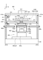
- the mounting board manufacturing device 10 of the present embodiment (hereinafter, also simply referred to as a manufacturing device 10) is a device for manufacturing a mounting board on which a plurality of electronic components are mounted.
- the manufacturing apparatus 10 includes a substrate transfer line 11, an information processing apparatus 20, a loader 50, a solder precoat forming apparatus 90, a solder precoat inspection apparatus 300, a flux coating apparatus 400, and electronic components. It includes mounting devices 501 and 502, a mounting state inspection device 600, a reflow device 700, a board inspection device 800, and an unloader 900. The components from the loader 50 to the unloader 900 are arranged from the upstream side to the downstream side in the order described. A known configuration may be applied to a configuration other than the configuration peculiar to the present disclosure.
- the electronic component mounting devices 501 and 502 may be collectively referred to as an electronic component mounting device 500.
- the substrate transfer line 11 transfers the substrate 1 (see FIG. 2) from the solder precoat forming apparatus 90 to the substrate inspection apparatus 800.
- the substrate transfer line 11 may be one continuous conveyor, or may be configured by arranging a plurality of conveyors in series.
- a conveyor using a known belt, chain, roller, transfer device, or the like can be used.
- the information processing device 20 is connected to other devices included in the manufacturing device 10 (solder precoat forming device 90, solder precoat inspection device 300, flux coating device 400, electronic component mounting device 500, reflow device 700, etc.) by wire or wirelessly. It is communicably connected by the local area network 20N. The information processing device 20 exchanges data with these devices. Thereby, the information processing apparatus 20 manages the process performed by the manufacturing apparatus 10.
- the information processing device 20 has an arithmetic processing unit and a storage device.
- the arithmetic processing unit is configured by a CPU (central processing unit) or the like.
- the storage device is composed of one or more RAMs (random access memory), a hard disk, and the like. These may be configured by another circuit or LSI (Large Scale Integrated Circuit), or may be configured integrally.
- the storage device stores programs required for each device of the manufacturing device 10 and data required for the programs.
- the loader 50 supplies the substrate housed in the rack (not shown) to the solder precoat forming apparatus 90.
- the unloader 900 collects the completed mounting board in a rack.
- Each device from the solder precoat forming device 90 to the board inspection device 800 includes a conveyor (board transfer line 11) for transporting the substrate.
- Each conveyor is arranged so that it can receive the substrate from the device on the upstream side (loader 50 side) and deliver it to the device on the downstream side (unloader 900 side).
- the solder precoat forming apparatus 90 is an apparatus for forming a solder precoat portion 3 (see FIG. 5) on the land 2 (see FIG. 5) of the substrate 1.
- the solder precoat forming apparatus 90 includes a solder paste supply unit 100, a heating unit 210, and a cooling unit 220. A part of the substrate transfer line 11 is arranged inside these.
- the solder paste supply unit 100 supplies the solder paste to the land 2 of the substrate 1 by, for example, a screen printing method.
- the heating unit 210 heats the solder paste supplied to the land 2 to melt the solder particles contained in the solder paste.
- the cooling unit 220 cools and solidifies the molten solder particles.
- the solder precoat portion 3 is formed on the land 2 of the substrate 1.
- the surface of the precoat portion 3 is accompanied by a residue of the flux component. This residue is obtained by the thermoplastic resin contained in the flux becoming liquid by heating, spreading on the surface of the precoat portion 3, and then solidifying into a film by cooling.
- the substrate 1 on which the precoat portion 3 is formed is conveyed to the solder precoat inspection device 300 by the substrate transfer line 11.
- solder precoat inspection device 300 is a device that inspects whether or not the precoat portion 3 is properly formed.
- the solder precoat inspection device 300 may detect, for example, the thickness of the precoat portion 3 and determine whether or not the precoat portion 3 is properly formed based on the detected thickness.
- the substrate 1 determined to have the precoat portion 3 properly formed is conveyed to the flux coating device 400 by the substrate transfer line 11.
- the flux coating device 400 is a device that applies flux for soldering by reflow onto the precoat portion 3.
- the method of applying the flux is not particularly limited.
- the flux may be applied onto the precoat portion 3 by a screen printing method using a mask and a squeegee, by a dispenser that ejects the flux from a nozzle, or by a sprayer that sprays the flux.
- the flux application device 400 is an example of a flux arrangement device. The configuration of the flux coating device 400 will be described in detail later.
- the substrate 1 coated with the flux is transferred to the electronic component mounting device 500 by the substrate transfer line 11.
- the electronic component mounting device 500 is a device for mounting electronic components (not shown) on the precoat portion 3 covered with flux.
- the electronic component mounting device 500 may mount the electronic component on the precoat portion 3 by using, for example, a suction nozzle (not shown) that sucks the electronic component.
- the board 1 on which the electronic components have been mounted is transported to the mounting state inspection device 600 by the board transport line 11.
- the mounting state inspection device 600 is a device that inspects the mounting state of electronic components.
- the mounting state inspection device 600 recognizes the mounting state such as the mounting position, posture, and presence / absence of electronic components by using an optical measuring device such as a camera or a three-dimensional measuring device, and they satisfy a predetermined standard. It may be determined whether or not.
- the board 1 for which the inspection has been completed is transported to the reflow device 700 by the substrate transfer line 11.
- the reflow device 700 heats the substrate 1 on which the electronic component is mounted to melt the precoat portion 3, and solders the electronic component to the land 2 (see FIG. 5). As a result, a mounting board on which electronic components are mounted is manufactured.
- the substrate 1 (mounting substrate) on which the soldering of the electronic components is completed is conveyed to the substrate inspection device 800 by the substrate transfer line 11.
- the board inspection device 800 is a device that inspects the quality of the mounting board.
- the substrate 1 (mounting substrate) that has been inspected by the substrate inspection device 800 is conveyed to the unloader 900 by the substrate transfer line 11.
- the unloader 900 collects the completed mounting board in a rack.
- the transport direction of the substrate 1 is the X direction
- the vertical direction is the Z direction
- the direction orthogonal to these is the Y direction.
- the axes extending along each direction are the X-axis, the Y-axis, and the Z-axis, respectively.
- support frames 411 are erected at both ends of the base 401 in the X direction.
- the components of the flux coating device 400 are arranged between these pair of support frames 411.
- a printing stage moving mechanism 403 and a printing stage 402 that moves by the printing stage moving mechanism 403 are provided on the upper surface of the base 401 between the pair of support frames 411.
- the print stage moving mechanism 403 has a structure in which the print stage elevating mechanism 403z is laminated on the print stage table 403xy ⁇ .
- the print stage 402 moves horizontally along the X-axis and the Y-axis, and rotates around the Z-axis.
- the print stage elevating mechanism 403z is driven, the print stage 402 moves up and down.
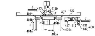
- the printing stage 402 has a function of holding the substrate 1 carried in from the upstream side and aligning the substrate 1 with respect to the mask plate 422 in which the pattern holes for printing (see FIG. 5) are formed.
- the mask plate 422 is an example of a mask.
- the printing stage 402 includes an elevating table 404 coupled to the printing stage elevating mechanism 403z.
- Support members 404a are erected at both ends of the upper surface of the elevating table 404.
- a holding block 404b extending in the X direction is coupled to the upper end portion of the support member 404a.
- a printing stage conveyor 406b provided with a drive belt for transporting the substrate 1 is provided on the inner surface of the holding block 404b.
- the printing stage conveyor 406b can be connected to the carry-in conveyor 406a and the carry-out conveyor 406c provided through the openings provided in the support frames 411 on the upstream side and the downstream side, respectively.
- the substrate 1 carried in by the carry-in conveyor 406a is delivered to the printing stage conveyor 406b and held by the printing stage 402. After the screen printing is completed on the printing stage 402, the substrate 1 is transferred from the printing stage conveyor 406b to the unloading conveyor 406c and carried out.
- the print stage conveyor 406b, the carry-in conveyor 406a, and the carry-out conveyor 406c each form a part of the substrate transfer line 11.
- a backup elevating mechanism 405a and a backup unit 405 that is driven up and down by the backup elevating mechanism 405a are provided on the upper surface of the elevating table 404.
- the backup unit 405 rises to support the lower surface of the substrate 1 conveyed by the printing stage conveyor 406b.
- side clampers 407 that grip the side surfaces of the substrate 1 are provided. These side clampers 407 are mutually openable and closable by a side clamper drive mechanism (not shown). By causing the side clamper 407 to perform a closing operation while the backup unit 405 supports the lower surface of the substrate 1, both side surfaces of the substrate 1 are sandwiched between the side clampers 407 in the printing stage 402. As a result, the substrate 1 is clamped and fixed.
- the printing stage 402 holding the substrate 1 is moved relative to the mask plate 422 and aligned.
- the print stage table 403xy ⁇ that horizontally moves the print stage 402 functions as an alignment mechanism that relatively moves the print stage 402 and the mask plate 422 in order to align the substrate 1 with the mask plate 422.
- a print head support beam 412 that supports the print head 413 is provided so as to be movable along the Y axis via the linear motion guide mechanism 412a.
- One end of the printhead support beam 412 is coupled to one support frame 411 via a printhead moving mechanism 414 configured as shown in FIG.
- the printhead moving mechanism 414 has a configuration in which a nut portion 414c to which a feed screw 414b rotationally driven by a printhead motor 414a is screwed is coupled to a printhead support beam 412.
- the print head 413 includes a pair of rear squeegees 413b and front squeegees 413c provided extending downward from the print head support beam 412.
- the squeegee drive unit 413a provided on the upper surface of the print head support beam 412
- either the rear squeegee 413b or the front squeegee 413c descends and lands on the mask plate 422 according to the direction of the squeezing operation.
- the rear squeegee 413b lands on the mask plate 422 when performing the squeezing operation in the left direction (first direction) in FIG.
- the front squeegee 413c lands on the mask plate 422 when performing the squeezing operation in the right direction (second direction) of FIG.
- the rear squeegee 413b is an example of the first squeegee.
- the front squeegee 413c is an example of a second squeegee.
- the rear squeegee 413b and the front squeegee 413c are examples of the coated portion, respectively.
- the mask plate 422 is formed with a pattern hole 422a which is a predetermined opening corresponding to the printing pattern on the substrate 1.
- the flux F for printing (see FIG. 4A and the like) is supplied to the upper surface of the mask plate 422.
- a squeezing operation using either the rear squeegee 413b or the front squeegee 413c on the upper surface of the mask plate 422.
- the flux F is printed on the substrate 1 in a predetermined print pattern through the pattern holes 422a.
- a camera moving mechanism 416 is provided between the upper surface of the printing stage 402 and the lower surface of the mask plate 422.
- the camera moving mechanism 416 moves the camera mounting base 417 to which the first camera 418 and the second camera 419 are mounted along the X-axis and the Y-axis.
- the camera movement mechanism 416 includes a camera X-axis movement mechanism 416X that moves the camera mounting base 417 along the camera X-axis beam 415 along the X-axis, and a camera Y-axis that moves the camera X-axis beam 415 along the Y-axis. It is composed of a moving mechanism 416Y.
- the movement of the camera X-axis beam 415 is guided by a linear motion guide mechanism 412a arranged on the inner surface of the support frame 411.
- the camera X-axis moving mechanism 416X includes a camera X-axis motor 415a and a feed screw 415b shown in FIG. 2, and a nut portion 415d shown in FIG.
- the camera mounting base 417 coupled to the nut portion 415d moves along the X-axis.
- the camera Y-axis moving mechanism 416Y includes a camera Y-axis motor 416a, a feed screw 416b, and a nut portion 416c coupled to the camera X-axis beam 415.
- the camera Y-axis motor 416a By driving the camera Y-axis motor 416a, the camera X-axis beam 415 coupled to the nut portion 416c moves along the Y-axis. As a result, the first camera 418 moves horizontally above the substrate 1 held by the print stage 402, and the second camera 419 moves horizontally below the mask plate 422.
- the first camera 418 is arranged with the imaging direction facing downward, and images the substrate 1 held on the printing stage 402. By recognizing the imaging result, the position of the substrate 1 and the position of the electrode to be printed on the substrate 1 are detected.
- the second camera 419 is arranged with the image pickup direction facing upward, and images a mask recognition mark (not shown) formed on the mask plate 422. By recognizing the imaging result, the positions of the mask center and the pattern hole 422a on the mask plate 422 are recognized.
- a roller mechanism 430 is fixed to the side surface of the camera X-axis beam 415.
- the roller mechanism 430 has a pressure cylinder 431 and a roller 432 connected to each other.
- the pressurizing cylinder 431 is fixed to the camera X-axis beam 415 and applies a downward force to the roller 432.
- the roller 432 extends along the X axis and is rotatable around a rotation axis extending in the X direction.
- the roller mechanism 430 including the roller 432 moves horizontally along the X-axis and the Y-axis with the horizontal movement of the camera X-axis beam 415.
- the roller mechanism 430 has a function of crushing the top of the precoat portion 3 of the substrate 1 by pressing the roller 432 against the substrate 1 by the pressure cylinder 431 while moving horizontally.
- the roller mechanism 430 is an example of a pressing device.
- Roller 432 is an example of a tool.
- the camera Y-axis moving mechanism 416Y functions as a horizontal moving mechanism that moves the roller 432 horizontally with respect to the substrate 1 held by the printing stage 402.
- the mounting substrate manufacturing method includes a paste placement step, a melt solidification step, a holding step, a breaking step, a substrate placement step, a flux placement step, a component mounting step, and a reflow step.
- the paste placement step is executed in the solder paste supply unit 100.
- the solder paste is placed on the land 2 of the substrate 1 by, for example, a flux printing method.
- the melt solidification step is executed in the heating unit 210 and the cooling unit 220.
- the solder paste is heated and melted by the heating unit 210, and then the molten solder paste is cooled and solidified by the cooling unit 220 to form the precoat portion 3 on the land 2.
- the holding step, the breaking step, the substrate placement step, and the flux placement step are executed by the flux coating device 400.
- the substrate 1 is held by the backup unit 405 and the side clamper 407.
- the backup elevating mechanism 405a is driven to raise the backup unit 405 in the printing stage 402 (arrow a), and the side clamper drive mechanism (not shown) is driven to drive the side clamper.
- the lower surface of the substrate 1 is supported by the backup unit 405 and the side surface is gripped by the side clamper 407 in a state where the upper surface thereof is substantially flush with the upper surface of the side clamper 407.
- the roller 432 is pressed against the precoat portion 3 to crush the precoat portion 3.
- the breaking step as shown in FIG. 4B, after the printing stage elevating mechanism 403z is driven to raise the printing stage 402 (arrow b), a downward force is applied to the roller 432 by the pressure cylinder 431.
- the roller 432 is pressed against the substrate 1 while moving along the Y axis (arrow c).
- the top of the precoat portion 3 of the substrate 1 is crushed flat.
- the residue existing in the form of a film at the top of the precoat portion 3 is cracked and the residue is destroyed. This exposes at least a portion of the solder from the cracks.
- the precoat portion 3 is crushed thinner than the thickness of the mask plate 422.
- the precoat portion 3 may be crushed to be thicker than the thickness of the mask plate 422, or may be crushed to the same thickness as the mask plate 422.
- the substrate 1 is brought into contact with the lower surface of the mask plate 422.
- the printing stage 402 is raised to hold the substrate 1 held by the backup unit 405 and the side clamper 407. It is brought into contact with the lower surface of the mask plate 422 (arrow e).
- the flux F is supplied to the upper surface of the mask plate 422, and the front squeegee 413c for performing the squeezing operation is in the print preparation position.
- the flux F is applied to the crushed precoat portion 3 with the rear squeegee 413b or the front squeegee 413c via the mask plate 422.
- the flux placement step as shown in FIG. 4C, the print head 413 is moved along the Y axis on the upper surface of the mask plate 422 (arrow f), and in this example, the front squeegee 413c is slid with respect to the mask plate 422.
- the squeezing operation of filling the pattern hole 422a with the flux F is executed.
- the flux F is applied to the precoat portion 3 of the substrate 1 via the pattern hole 422a of the mask plate 422.
- the flux F is also applied to the top of the precoat portion 3 with a certain thickness. This is because the precoat portion 3 is crushed thinner than the thickness of the mask plate 422 in the previous breaking step.
- the flux placement step is preferably executed within 30 seconds after the execution of the breaking step, and more preferably within 10 seconds after the execution of the breaking step.
- the time from the end time of the breaking step to the start time of the flux placement step is preferably 30 seconds or less, and more preferably 10 seconds or less.
- the component mounting process is executed in the electronic component mounting device 500.
- the electronic component is mounted on the substrate 1 with the terminals of the electronic component aligned with the precoat portion 3.
- the electronic component can be easily mounted. This is because the top of the precoat portion 3 is flat, so that it is easy to mount the electronic component, and the viscosity of the flux F makes it easy for the electronic component to be held on the precoat portion 3.
- the reflow process is executed in the reflow device 700.
- the substrate 1 on which the electronic component is mounted is heated to melt the precoat portion 3 and the terminals of the electronic component are soldered to the land 2.
- Embodiment 2 The second embodiment of the present disclosure will be described.
- the mounting substrate manufacturing apparatus 10 of the present embodiment is different from the above-described first embodiment in that the configuration of the flux coating apparatus 400 is a fixed type of the roller mechanism 430.
- the differences from the first embodiment will be mainly described.
- the pressure cylinder 431 of the roller mechanism 430 is fixed to the beam 408 fixed in the flux application device 400. Therefore, in this embodiment, the roller 432 does not move along the Y axis.
- the print stage 402 is moved from the print position shown in FIG. 6 to the destruction position (not shown) by the print stage moving mechanism 403.
- the breaking position is the position where the printing stage 402 exists below the roller mechanism 430.
- the printing stage 402 is moved along the Y axis at the breaking position and the roller 432 is pressed against the substrate 1 to crush the top of the precoat portion 3 of the substrate 1.
- the residue on the surface is destroyed at the top of the precoat portion 3, and at least a part of the solder inside thereof is exposed.
- the printing stage moving mechanism 403 functions as a horizontal moving mechanism that moves the roller 432 horizontally with respect to the substrate 1 held by the printing stage 402.
- Embodiment 3 The third embodiment of the present disclosure will be described.
- the mounting substrate manufacturing apparatus 10 of the present embodiment is different from the above-described second embodiment in the configuration of the tool for crushing the precoat portion 3 in the flux coating apparatus 400.
- the differences from the second embodiment will be mainly described.
- a plate mechanism 440 is fixed to the beam 408.
- the plate mechanism 440 has a pressure cylinder 441 and a horizontal plate 442 connected to each other.
- the pressure cylinder 441 is fixed to the beam 408 and applies a downward force to the horizontal plate 442.
- the horizontal plate 442 extends along the horizontal plane and is movable along the Z axis.
- the lower surface of the horizontal plate 442 is substantially flat.
- the plate mechanism 440 has a function of crushing the top of the precoat portion 3 of the substrate 1 by pressing the horizontal plate 442 against the substrate 1 at the fracture position by the pressure cylinder 441.
- the plate mechanism 440 is an example of a pressing device.
- the horizontal plate 442 is an example of a tool.
- substantially flat includes not only completely flat ones but also those that are generally flat but have irregularities. For example, when the top of the precoat portion 3 is crushed by using a roller 432 having an uneven surface, the latter shape can be obtained.
- Embodiment 4 of the present disclosure will be described.
- the mounting substrate manufacturing apparatus 10 of the present embodiment is different from the above-described first embodiment in the configuration of the print head 413 of the flux coating device 400 and the mode of use of the flux coating device 400.
- the differences from the first embodiment will be mainly described.
- the print head 413 has a roller mechanism 430 provided between the rear squeegee 413b and the front squeegee 413c. Except for such an arrangement, the configuration of the roller mechanism 430 is the same as that of the first embodiment.
- the roller mechanism 430 presses the roller 432 against the precoat portion 3 of the substrate 1 via the mask plate 422 while moving horizontally together with the rear squeegee 413b and the front squeegee 413c.
- the roller mechanism 430 may be provided on the right side of the rear squeegee 413b or on the left side of the front squeegee 413c in FIG.
- the print head moving mechanism 414 moves the roller 432 horizontally with respect to the substrate 1 held by the print stage 402. Functions as.
- the method of using the flux coating device 400 of the present embodiment includes a holding step (here, illustration and description are omitted), a substrate arranging step, a breaking step, and a flux arranging step.
- the substrate 1 is arranged by providing a gap with the mask plate 422 below the mask plate 422.
- the printing stage 402 is raised so that the substrate 1 held by the backup unit 405 and the side clamper 407 is placed below the mask plate 422 with a gap. Provide and arrange.
- the roller 432 is pressed against the precoat portion 3 with the first load via the mask plate 422 to crush the precoat portion 3.
- the breaking step as shown in the second and third stages from the top of FIG. 9, the print head 413 is moved along the Y axis while pressing the roller 432 against the mask plate 422 with a relatively large first load. Let me.
- the mask plate 422 is locally in close contact with the substrate 1 at the position where the roller 432 is pressed.
- the thickness of the precoat portion 3 crushed by the roller 432 that moves in this way becomes substantially the same as the thickness of the mask plate 422, or becomes slightly thinner than the thickness.
- the precoat portion 3 is crushed, the surface residue is destroyed at the top thereof, and at least a part of the solder inside thereof is exposed.
- the flux F is applied to the crushed precoat portion 3 with the rear squeegee 413b or the front squeegee 413c with a second load smaller than the first load, via the mask plate 422.
- the flux placement step as shown in the third and fourth stages from the top of FIG. 9, in this example, the front squeegee 413c is pressed against the mask plate 422 with a relatively small second load, and the print head 413 is Y. Move in the direction (second direction). As a result, at the place where the front squeegee 413c is pressed, the mask plate 422 is pushed down weaker than the above-mentioned breaking step.
- the flux F is filled in the pattern hole 422a by the front squeegee 413c that moves in this way, the flux F is also applied to the top of the precoat portion 3 with a certain thickness. As a result, it is possible to more easily mount the electronic component by the electronic component mounting device 500.
- the flux placement step is preferably executed within 30 seconds after the execution of the breaking step, and more preferably within 10 seconds after the execution of the breaking step.
- the time from the end time of the breaking step to the start time of the flux placement step is preferably 30 seconds or less, and more preferably 10 seconds or less.
- Embodiment 5 The fifth embodiment of the present disclosure will be described.
- the mounting substrate manufacturing apparatus 10 of the present embodiment is different from the above-described 4 in the configuration of the roller mechanism 430 of the flux coating device 400 and the mode of using the flux coating device 400.
- the differences from the fourth embodiment will be mainly described.
- the roller 432 of the roller mechanism 430 has irregularities on the outer peripheral surface. Except for this point, the configuration of the roller mechanism 430 is the same as that of the fourth embodiment.
- the roller mechanism 430 presses the roller 432 against the precoat portion 3 of the substrate 1 via the mask plate 422 while moving horizontally together with the rear squeegee 413b and the front squeegee 413c.
- the method of using the flux coating device 400 of the present embodiment includes a holding step (here, illustration and description are omitted), a substrate arranging step, a breaking step, and a flux arranging step.
- the substrate 1 is arranged under the mask plate 422 in contact with the mask plate 422.
- the printing stage 402 is raised so that the substrate 1 held by the backup unit 405 and the side clamper 407 is brought into contact with the mask plate 422 under the mask plate 422. And place it.
- the roller 432 is pressed against the precoat portion 3 with the first load via the mask plate 422 to crush the precoat portion 3.
- the breaking step as shown in the second and third stages from the top of FIG. 10, the print head 413 is moved along the Y axis while pressing the roller 432 against the mask plate 422 with a relatively large first load. Let me. As a result, the mask plate 422 is strongly crushed locally where the roller 432 is pressed. The thickness of the precoat portion 3 crushed by the roller 432 that moves in this way is slightly thinner than the thickness of the mask plate 422. Further, since the outer peripheral surface of the roller 432 has irregularities, the top of the precoat portion 3 is crushed into a shape with irregularities. When the precoat portion 3 is crushed, the surface residue is destroyed at the top thereof, and at least a part of the solder inside thereof is exposed.
- the flux F is applied to the crushed precoat portion 3 with the rear squeegee 413b or the front squeegee 413c with a second load smaller than the first load, via the mask plate 422.
- the flux placement step as shown in the third and fourth stages from the top of FIG. 10, in this example, the front squeegee 413c is pressed against the mask plate 422 with a relatively small second load, and the print head 413 is Y. Move in the direction (second direction). As a result, the mask plate 422 is crushed weaker than the above-mentioned breaking step at the place where the front squeegee 413c is pressed.
- the flux F is filled in the pattern hole 422a by the front squeegee 413c that moves in this way, the flux F is also applied to the top of the precoat portion 3 with a certain thickness. Further, the flux F is filled in the unevenness of the top of the precoat portion 3. As a result, it is possible to more easily mount the electronic component by the electronic component mounting device 500.
- the flux placement step is preferably executed within 30 seconds after the execution of the breaking step, and more preferably within 10 seconds after the execution of the breaking step.
- the time from the end time of the breaking step to the start time of the flux placement step is preferably 30 seconds or less, and more preferably 10 seconds or less.
- This disclosure can be used for mounting board manufacturing methods and flux coating devices.
- Substrate 2 Land 3: Precoat section 10: Mounting board manufacturing device 11: Board transfer line 20: Information processing device 20N: Local area network 50: Loader 90: Solder precoat forming device 100: Solder paste supply section 210: Heating section 220: Cooling unit 300: Solder precoat inspection device 400: Flux coating device (flux placement device) 401: Base 402: Printing stage 403: Printing stage moving mechanism 403xy ⁇ : Printing stage table 403z: Printing stage elevating mechanism 404: Elevating table 404a: Support member 404b: Holding block 405: Backup unit 405a: Backup elevating mechanism 406a: Carry-in conveyor 406b: Printing stage conveyor 406c: Carrying out conveyor 407: Side clamper 408: Beam 411: Support frame 412: Printing head support beam 412a: Linear guide mechanism 413: Printing head 413a: Squeegee drive unit 413b: Rear squeegee (coating unit) 413c:
Landscapes
- Engineering & Computer Science (AREA)
- Microelectronics & Electronic Packaging (AREA)
- Manufacturing & Machinery (AREA)
- Mechanical Engineering (AREA)
- Electric Connection Of Electric Components To Printed Circuits (AREA)
Abstract
Description
本開示に係る実装基板製造方法は、基板のランドに電子部品の端子を半田付けする実装基板製造方法であって、前記ランドに半田ペーストを配置するペースト配置工程と、前記半田ペーストを溶融および固化させて前記ランド上に半田のプリコート部を作る溶融固化工程と、前記プリコート部にツールを押し当てることにより前記プリコート部の表面を覆う残渣を破壊する破壊工程と、前記プリコート部にフラックスを配置するフラックス配置工程と、前記電子部品の端子を前記プリコート部に位置合わせした状態で前記電子部品を前記基板に搭載する部品搭載工程と、前記基板を加熱して前記プリコート部を溶融させて前記端子を前記ランドに半田付けするリフロー工程と、を備える。
本開示に係るフラックス塗布装置は、上述の実装基板製造方法で使用され、基板に形成された半田のプリコート部にスクリーン印刷法によってフラックスを塗布するフラックス塗布装置であって、前記フラックスを塗布する前に前記プリコート部の表面を覆う残渣に押し当てられて前記残渣を破壊するツールを備える。
本開示の実施形態1について説明する。本実施形態の実装基板製造装置10(以下、単に製造装置10ともいう。)は、複数の電子部品が実装された実装基板を製造するための装置である。
図1に示すように、製造装置10は、基板搬送ライン11と、情報処理装置20と、ローダ50と、半田プリコート形成装置90と、半田プリコート検査装置300と、フラックス塗布装置400と、電子部品搭載装置501,502と、搭載状態検査装置600と、リフロー装置700と、基板検査装置800と、アンローダ900とを備える。ローダ50からアンローダ900までの構成要素は、この記載順に上流側から下流側に配置されている。本開示に特有の構成以外の構成には、公知の構成を適用してもよい。以下では、電子部品搭載装置501,502をまとめて、電子部品搭載装置500ということがある。
基板搬送ライン11は、半田プリコート形成装置90から基板検査装置800にわたって基板1(図2を参照)を搬送する。基板搬送ライン11は、連続した1つのコンベアであってもよく、または複数のコンベアを直列に並べて構成されてもよい。基板搬送ライン11には、公知のベルト、チェーン、ローラ、移載装置などを使用したコンベアを用いることができる。
情報処理装置20は、製造装置10に含まれる他の装置(半田プリコート形成装置90、半田プリコート検査装置300、フラックス塗布装置400、電子部品搭載装置500、リフロー装置700など)に、有線または無線のローカルエリアネットワーク20Nによって通信可能に接続されている。情報処理装置20は、これらの装置との間でデータをやり取りする。それによって、情報処理装置20は、製造装置10で行われる工程を管理する。
ローダ50は、ラック(図示せず)に収納された基板を半田プリコート形成装置90へ供給する。アンローダ900は、完成した実装基板をラックに回収する。半田プリコート形成装置90から基板検査装置800までの各装置は、基板を搬送するコンベア(基板搬送ライン11)を含む。各コンベアは、上流側(ローダ50側)の装置から基板を受け取って下流側(アンローダ900側)の装置へ受け渡すことができるように配置される。
半田プリコート形成装置90は、基板1のランド2(図5を参照)に半田のプリコート部3(図5を参照)を形成する装置である。半田プリコート形成装置90は、半田ペースト供給部100と、加熱部210と、冷却部220とを有する。これらの内部には、基板搬送ライン11の一部が配置される。
半田プリコート検査装置300は、プリコート部3が適正に形成されているかどうかを検査する装置である。半田プリコート検査装置300は、例えば、プリコート部3の厚みを検出し、検出した厚みに基づいてプリコート部3が適正に形成されているかどうかを判定してもよい。プリコート部3が適正に形成されていると判定された基板1は、基板搬送ライン11によってフラックス塗布装置400へ搬送される。
フラックス塗布装置400は、リフローによる半田付けのためのフラックスを、プリコート部3上に塗布する装置である。フラックスの塗布方法に特に限定はない。例えば、フラックスは、マスクとスキージを用いるスクリーン印刷法により、ノズルからフラックスを吐出するディスペンサにより、またはフラックスを噴霧する噴霧器により、プリコート部3上に塗布されてもよい。フラックス塗布装置400は、フラックス配置装置の一例である。フラックス塗布装置400の構成について、詳しくは後述する。フラックスが塗布された基板1は、基板搬送ライン11によって電子部品搭載装置500へ搬送される。
電子部品搭載装置500は、フラックスで覆われたプリコート部3に電子部品(図示せず)を搭載する装置である。電子部品搭載装置500は、例えば、電子部品を吸着する吸着ノズル(図示せず)を用いてプリコート部3に電子部品を搭載してもよい。電子部品の搭載が完了した基板1は、基板搬送ライン11によって搭載状態検査装置600へ搬送される。
搭載状態検査装置600は、電子部品の搭載状態を検査する装置である。搭載状態検査装置600は、例えば、カメラや三次元計測機などの光学的な計測装置を用いて、電子部品の搭載位置、姿勢、有無などの搭載状態を認識し、それらが所定の基準を満たすかどうかを判定してもよい。検査が完了した基板1は、基板搬送ライン11によってリフロー装置700へ搬送される。
リフロー装置700は、電子部品が搭載された基板1を加熱してプリコート部3を溶融し、電子部品をランド2(図5を参照)に半田付けする。これにより、電子部品が実装された実装基板が製造される。電子部品の半田付けが完了した基板1(実装基板)は、基板搬送ライン11によって基板検査装置800へ搬送される。
基板検査装置800は、実装基板の良否を検査する装置である。基板検査装置800での検査が終了した基板1(実装基板)は、基板搬送ライン11によってアンローダ900へ搬送される。アンローダ900は、完成した実装基板をラックに回収する。
次に、フラックス塗布装置400について、図2および図3を参照して詳しく説明する。なお、以下の説明では、基板1の搬送方向をX方向とし、鉛直方向をZ方向とし、これらに直交する方向をY方向とする。また、各方向に沿って延びる軸をそれぞれX軸、Y軸、およびZ軸とする。
次に、本実施形態の実装基板方法について、図面を適宜参照して説明する。実装基板製造方法は、ペースト配置工程と、溶融固化工程と、保持工程と、破壊工程と、基板配置工程と、フラックス配置工程と、部品搭載工程と、リフロー工程とを備える。
本開示の実施形態2について説明する。本実施形態の実装基板製造装置10は、フラックス塗布装置400の構成が、ローラ機構430が固定式である点で上記実施形態1と異なる。以下、上記実施形態1と異なる点について主に説明する。
本開示の実施形態3について説明する。本実施形態の実装基板製造装置10は、フラックス塗布装置400において、プリコート部3を押し潰すためのツールの構成が上記実施形態2と異なる。以下、上記実施形態2と異なる点について主に説明する。
本開示の実施形態4について説明する。本実施形態の実装基板製造装置10は、フラックス塗布装置400の印刷ヘッド413の構成、およびフラックス塗布装置400の使用方法の態様が上記実施形態1と異なる。以下、上記実施形態1と異なる点について主に説明する。
図8に示すように、印刷ヘッド413は、後スキージ413bと前スキージ413cとの間に設けられたローラ機構430を有する。このような配置を除き、ローラ機構430の構成は上記実施形態1のそれと同様である。ローラ機構430は、後スキージ413bおよび前スキージ413cと共に水平移動しながら、マスクプレート422を介して基板1のプリコート部3にローラ432を押し当てる。なお、ローラ機構430は、図8において、後スキージ413bの右方に設けられていてもよいし、前スキージ413cの左方に設けられていてもよい。本実施形態のようにローラ432を印刷ヘッド413に一体的に設ける場合、印刷ヘッド移動機構414は、ローラ432を印刷ステージ402に保持された基板1に対して相対的に水平移動させる水平移動機構として機能する。
本実施形態のフラックス塗布装置400の使用方法について、図9を参照して説明する。図9に示すように、フラックス塗布装置400の使用方法は、保持工程(ここでは、図示と説明を省略する。)と、基板配置工程と、破壊工程と、フラックス配置工程とを備える。
本開示の実施形態5について説明する。本実施形態の実装基板製造装置10は、フラックス塗布装置400のローラ機構430の構成、およびフラックス塗布装置400の使用方法の態様が上記実施形態4と異なる。以下、上記実施形態4と異なる点について主に説明する。
図10に示すように、ローラ機構430のローラ432は、外周面に凹凸を有する。この点を除き、ローラ機構430の構成は上記実施形態4のそれと同様である。ローラ機構430は、後スキージ413bおよび前スキージ413cと共に水平移動しながら、マスクプレート422を介して基板1のプリコート部3にローラ432を押し当てる。
本実施形態のフラックス塗布装置400の使用方法について、図10を参照して説明する。図10に示すように、フラックス塗布装置400の使用方法は、保持工程(ここでは、図示と説明を省略する。)と、基板配置工程と、破壊工程と、フラックス配置工程とを備える。
2:ランド
3:プリコート部
10:実装基板製造装置
11:基板搬送ライン
20:情報処理装置
20N:ローカルエリアネットワーク
50:ローダ
90:半田プリコート形成装置
100:半田ペースト供給部
210:加熱部
220:冷却部
300:半田プリコート検査装置
400:フラックス塗布装置(フラックス配置装置)
401:基台
402:印刷ステージ
403:印刷ステージ移動機構
403xyθ:印刷ステージテーブル
403z:印刷ステージ昇降機構
404:昇降テーブル
404a:支持部材
404b:保持ブロック
405:バックアップ部
405a:バックアップ昇降機構
406a:搬入コンベア
406b:印刷ステージコンベア
406c:搬出コンベア
407:サイドクランパ
408:梁
411:支持フレーム
412:印刷ヘッド支持ビーム
412a:直動ガイド機構
413:印刷ヘッド
413a:スキージ駆動部
413b:後スキージ(塗布部)
413c:前スキージ(塗布部)
414:印刷ヘッド移動機構
414a:印刷ヘッドモータ
414b:送りねじ
414c:ナット部
415:カメラX軸ビーム
415a:カメラX軸モータ
415b:送りねじ
415d:ナット部
416:カメラ移動機構
416a:カメラY軸モータ
416b:送りねじ
416c:ナット部
416X:カメラX軸移動機構
416Y:カメラY軸移動機構
417:カメラ取付ベース
418:第1カメラ
419:第2カメラ
422:マスクプレート
422a:パターン孔
430:ローラ機構(押当装置)
431:加圧シリンダ
432:ローラ(ツール)
440:プレート機構(押当装置)
441:加圧シリンダ
442:水平プレート(ツール)
500:電子部品搭載装置
501:電子部品搭載装置
502:電子部品搭載装置
600:搭載状態検査装置
700:リフロー装置
800:基板検査装置
900:アンローダ
F:フラックス
Claims (13)
- 基板のランドに電子部品の端子を半田付けする実装基板製造方法であって、
前記ランドに半田ペーストを配置するペースト配置工程と、
前記半田ペーストを溶融および固化させて前記ランド上に半田のプリコート部を作る溶融固化工程と、
前記プリコート部にツールを押し当てることにより前記プリコート部の表面を覆う残渣を破壊する破壊工程と、
前記プリコート部にフラックスを配置するフラックス配置工程と、
前記電子部品の端子を前記プリコート部に位置合わせした状態で前記電子部品を前記基板に搭載する部品搭載工程と、
前記基板を加熱して前記プリコート部を溶融させて前記端子を前記ランドに半田付けするリフロー工程と、
を備える、実装基板製造方法。 - 前記破壊工程において、前記ツールで前記プリコート部の頂部を平坦状または凹凸状にする、請求項1に記載の実装基板製造方法。
- 前記フラックス配置工程は、フラックスを基板に配置するフラックス配置装置で実行し、
前記破壊工程は、前記フラックス配置装置が有する押当装置で実行する、請求項1または2に記載の実装基板製造方法。 - 前記フラックス配置工程は、前記破壊工程の実行後30秒以内に実行する、請求項1~3のいずれか1項に記載の実装基板製造方法。
- 請求項1~4のいずれか1項に記載の実装基板製造方法で使用され、基板に形成された半田のプリコート部にスクリーン印刷法によってフラックスを塗布するフラックス塗布装置であって、
前記フラックスを塗布する前に前記プリコート部の表面を覆う残渣に押し当てられて前記残渣を破壊するツールを備える、フラックス塗布装置。 - 前記基板のうちフラックスを塗布しない領域を覆うと共に、厚さ方向に貫通したパターン孔を有するマスクと、
前記マスク上に配置されたフラックスを、前記パターン孔を介して前記プリコート部に塗布する少なくとも1つのスキージを有する印刷ヘッドと、
前記基板を保持する印刷ステージと、
前記ツールを、前記印刷ステージに保持された前記基板に対して相対的に水平移動させる水平移動機構と、
をさらに備える、請求項5に記載のフラックス塗布装置。 - 前記基板を撮像するカメラをさらに備え、
前記水平移動機構は、前記印刷ステージに保持された前記基板の上方で前記カメラを水平移動させるカメラ移動機構である、請求項6に記載のフラックス塗布装置。 - 前記印刷ヘッドを前記マスクに対して水平方向へ移動させる印刷ヘッド移動機構をさらに備えるか、または、
前記ツールは、前記印刷ヘッドに設けられ、前記水平移動機構は、前記印刷ヘッド移動機構を兼ねる、請求項6に記載のフラックス塗布装置。 - 前記印刷ヘッドは、第1方向に水平移動しながら前記プリコート部にフラックスを塗布する第1スキージと、前記第1方向と逆の第2方向に水平移動しながら前記プリコート部にフラックスを塗布する第2スキージと、を有し、
前記ツールは、前記第1スキージと前記第2スキージとの間に設けられている、請求項6~8のいずれか1項に記載のフラックス塗布装置。 - 前記印刷ステージを水平移動させる印刷ステージ移動機構をさらに備え、
前記水平移動機構は、前記印刷ステージ移動機構である、請求項6に記載のフラックス塗布装置。 - 前記ツールは、前記基板に対して相対的に水平移動するローラである、請求項5~10のいずれか1項に記載のフラックス塗布装置。
- 前記ローラは、外周面に凹凸を有する、請求項11に記載のフラックス塗布装置。
- 前記ツールは、前記基板に対して相対的に鉛直移動する水平プレートである、請求項5~10のいずれか1項に記載のフラックス塗布装置。
Priority Applications (3)
| Application Number | Priority Date | Filing Date | Title |
|---|---|---|---|
| US18/043,955 US20240015893A1 (en) | 2020-09-14 | 2021-07-05 | Mounting board manufacturing method and flux coating device |
| JP2022547412A JPWO2022054384A1 (ja) | 2020-09-14 | 2021-07-05 | |
| CN202180055176.5A CN116096520A (zh) | 2020-09-14 | 2021-07-05 | 安装基板制造方法及助熔剂涂布装置 |
Applications Claiming Priority (4)
| Application Number | Priority Date | Filing Date | Title |
|---|---|---|---|
| JP2020-154142 | 2020-09-14 | ||
| JP2020154141 | 2020-09-14 | ||
| JP2020-154141 | 2020-09-14 | ||
| JP2020154142 | 2020-09-14 |
Publications (1)
| Publication Number | Publication Date |
|---|---|
| WO2022054384A1 true WO2022054384A1 (ja) | 2022-03-17 |
Family
ID=80632234
Family Applications (1)
| Application Number | Title | Priority Date | Filing Date |
|---|---|---|---|
| PCT/JP2021/025337 WO2022054384A1 (ja) | 2020-09-14 | 2021-07-05 | 実装基板製造方法およびフラックス塗布装置 |
Country Status (4)
| Country | Link |
|---|---|
| US (1) | US20240015893A1 (ja) |
| JP (1) | JPWO2022054384A1 (ja) |
| CN (1) | CN116096520A (ja) |
| WO (1) | WO2022054384A1 (ja) |
Citations (3)
| Publication number | Priority date | Publication date | Assignee | Title |
|---|---|---|---|---|
| JPH08250846A (ja) * | 1995-03-07 | 1996-09-27 | Matsushita Electric Ind Co Ltd | 電子部品の半田付け用フラックスおよびその塗布装置および電子部品の半田付け方法 |
| JPH09321425A (ja) * | 1996-05-28 | 1997-12-12 | Nippon Antomu Kogyo Kk | チップ状電子部品の実装方法 |
| JP2005116917A (ja) * | 2003-10-10 | 2005-04-28 | Omron Corp | 部品実装基板の製作方法およびフラックス塗布装置 |
-
2021
- 2021-07-05 CN CN202180055176.5A patent/CN116096520A/zh active Pending
- 2021-07-05 JP JP2022547412A patent/JPWO2022054384A1/ja active Pending
- 2021-07-05 WO PCT/JP2021/025337 patent/WO2022054384A1/ja active Application Filing
- 2021-07-05 US US18/043,955 patent/US20240015893A1/en active Pending
Patent Citations (3)
| Publication number | Priority date | Publication date | Assignee | Title |
|---|---|---|---|---|
| JPH08250846A (ja) * | 1995-03-07 | 1996-09-27 | Matsushita Electric Ind Co Ltd | 電子部品の半田付け用フラックスおよびその塗布装置および電子部品の半田付け方法 |
| JPH09321425A (ja) * | 1996-05-28 | 1997-12-12 | Nippon Antomu Kogyo Kk | チップ状電子部品の実装方法 |
| JP2005116917A (ja) * | 2003-10-10 | 2005-04-28 | Omron Corp | 部品実装基板の製作方法およびフラックス塗布装置 |
Also Published As
| Publication number | Publication date |
|---|---|
| US20240015893A1 (en) | 2024-01-11 |
| JPWO2022054384A1 (ja) | 2022-03-17 |
| CN116096520A (zh) | 2023-05-09 |
Similar Documents
| Publication | Publication Date | Title |
|---|---|---|
| TWI351905B (ja) | ||
| JP4816194B2 (ja) | 電子部品実装システムおよび電子部品搭載装置ならびに電子部品実装方法 | |
| US6460755B1 (en) | Bump forming method and apparatus therefor | |
| JP6643577B2 (ja) | 印刷装置および半田管理システム | |
| JP4896655B2 (ja) | 実装不良の原因特定方法および実装基板製造装置 | |
| TW200945978A (en) | Solder ball printing device | |
| JP6694778B2 (ja) | スクリーン印刷装置 | |
| WO2022054384A1 (ja) | 実装基板製造方法およびフラックス塗布装置 | |
| JP5739754B2 (ja) | 電子回路部品の立上がり防止方法および電子回路製造システム | |
| JP2006108200A (ja) | はんだ印刷システム | |
| JP4532694B2 (ja) | 3次元データ取得方法,装置、およびマスク印刷方法、装置 | |
| JP2004155185A (ja) | はんだペースト印刷方法、はんだペースト印刷装置、はんだ印刷層を有する配線基板の製造方法 | |
| JP2006272583A (ja) | スクリーン印刷装置およびスクリーン印刷方法ならびに基板 | |
| GB2351347A (en) | Inspecting printing state of pattern eg on a printed circuit board | |
| JP2004111424A (ja) | 部品実装装置及び部品実装方法 | |
| JP2023120046A (ja) | 基板押圧装置および基板押圧方法 | |
| JP4118286B2 (ja) | 半田ボール搭載方法 | |
| JP3666468B2 (ja) | 電子部品実装装置および電子部品実装方法 | |
| JP2005199545A (ja) | スクリーン印刷装置およびスクリーン印刷方法 | |
| JP6892510B2 (ja) | スクリーン印刷機 | |
| JP4595857B2 (ja) | 電子部品実装システムおよび電子部品実装方法 | |
| JP7117613B2 (ja) | 電子部品実装システム | |
| JP6719050B2 (ja) | 電子部品実装システム | |
| JPH0964521A (ja) | 半田供給装置及び半田供給方法 | |
| JP4231799B2 (ja) | スクリーン印刷方法及びスクリーン印刷機 |
Legal Events
| Date | Code | Title | Description |
|---|---|---|---|
| 121 | Ep: the epo has been informed by wipo that ep was designated in this application |
Ref document number: 21866344 Country of ref document: EP Kind code of ref document: A1 |
|
| ENP | Entry into the national phase |
Ref document number: 2022547412 Country of ref document: JP Kind code of ref document: A |
|
| WWE | Wipo information: entry into national phase |
Ref document number: 18043955 Country of ref document: US |
|
| NENP | Non-entry into the national phase |
Ref country code: DE |
|
| 122 | Ep: pct application non-entry in european phase |
Ref document number: 21866344 Country of ref document: EP Kind code of ref document: A1 |