WO2022050337A1 - ベイパーチャンバー、及び、これを搭載する半導体パッケージ - Google Patents
ベイパーチャンバー、及び、これを搭載する半導体パッケージ Download PDFInfo
- Publication number
- WO2022050337A1 WO2022050337A1 PCT/JP2021/032236 JP2021032236W WO2022050337A1 WO 2022050337 A1 WO2022050337 A1 WO 2022050337A1 JP 2021032236 W JP2021032236 W JP 2021032236W WO 2022050337 A1 WO2022050337 A1 WO 2022050337A1
- Authority
- WO
- WIPO (PCT)
- Prior art keywords
- vapor chamber
- diffusion member
- heat diffusion
- heat
- chamber body
- Prior art date
- Legal status (The legal status is an assumption and is not a legal conclusion. Google has not performed a legal analysis and makes no representation as to the accuracy of the status listed.)
- Ceased
Links
Images


Classifications
-
- H—ELECTRICITY
- H10—SEMICONDUCTOR DEVICES; ELECTRIC SOLID-STATE DEVICES NOT OTHERWISE PROVIDED FOR
- H10W—GENERIC PACKAGES, INTERCONNECTIONS, CONNECTORS OR OTHER CONSTRUCTIONAL DETAILS OF DEVICES COVERED BY CLASS H10
- H10W40/00—Arrangements for thermal protection or thermal control
- H10W40/70—Fillings or auxiliary members in containers or in encapsulations for thermal protection or control
- H10W40/73—Fillings or auxiliary members in containers or in encapsulations for thermal protection or control for cooling by change of state
-
- H—ELECTRICITY
- H10—SEMICONDUCTOR DEVICES; ELECTRIC SOLID-STATE DEVICES NOT OTHERWISE PROVIDED FOR
- H10W—GENERIC PACKAGES, INTERCONNECTIONS, CONNECTORS OR OTHER CONSTRUCTIONAL DETAILS OF DEVICES COVERED BY CLASS H10
- H10W40/00—Arrangements for thermal protection or thermal control
- H10W40/01—Manufacture or treatment
- H10W40/03—Manufacture or treatment of arrangements for cooling
- H10W40/037—Assembling together parts thereof
-
- H—ELECTRICITY
- H10—SEMICONDUCTOR DEVICES; ELECTRIC SOLID-STATE DEVICES NOT OTHERWISE PROVIDED FOR
- H10W—GENERIC PACKAGES, INTERCONNECTIONS, CONNECTORS OR OTHER CONSTRUCTIONAL DETAILS OF DEVICES COVERED BY CLASS H10
- H10W40/00—Arrangements for thermal protection or thermal control
- H10W40/20—Arrangements for cooling
- H10W40/25—Arrangements for cooling characterised by their materials
- H10W40/258—Metallic materials
-
- H—ELECTRICITY
- H10—SEMICONDUCTOR DEVICES; ELECTRIC SOLID-STATE DEVICES NOT OTHERWISE PROVIDED FOR
- H10W—GENERIC PACKAGES, INTERCONNECTIONS, CONNECTORS OR OTHER CONSTRUCTIONAL DETAILS OF DEVICES COVERED BY CLASS H10
- H10W40/00—Arrangements for thermal protection or thermal control
- H10W40/40—Arrangements for thermal protection or thermal control involving heat exchange by flowing fluids
- H10W40/47—Arrangements for thermal protection or thermal control involving heat exchange by flowing fluids by flowing liquids, e.g. forced water cooling
Definitions
- the present invention relates to a vapor chamber having a heat diffusion member.
- a vapor chamber may be used as an example of a means for suppressing a temperature rise of a semiconductor package.
- it is necessary to smoothly evaporate and condense the liquid material enclosed in the chamber body of the vapor chamber. If the balance between evaporation and condensation is greatly lost, a decrease in heat transport called dryout occurs, so it is necessary to consider the effective area of the evaporation part and the condensation part.
- Patent Document 1 As a vapor chamber with improved heat transport capacity, for example, in Patent Document 1, a large number of fins are provided inside the chamber body of the vapor chamber, and the fins are connected to the upper plate or the lower plate to reduce the flow rate of the liquid material. It is disclosed to increase and increase heat transport. Further, Patent Document 2 discloses that the vapor chamber and the substrate are connected via a heat conductive portion such as metal, and the heat accumulated in the vapor chamber is transferred to the substrate side.
- a heat conductive portion such as metal
- One aspect of the present invention is to provide a vapor chamber capable of suppressing a temperature rise of a semiconductor element by efficiently transporting heat generated from the semiconductor element, and a semiconductor package on which the vapor chamber is mounted. And.
- the present inventors have found that arranging the heat diffusion member on the surface of the chamber body of the vapor chamber is effective in improving the substantially effective area of the evaporating portion, and the vapor chamber It has been found that the temperature rise of the semiconductor element can be suppressed by increasing the heat transport amount, and the present invention has been completed.
- the vapor chamber according to one aspect of the present invention relates to the following.
- the chamber body has a first outer surface, a first inner surface which is a back surface of the first outer surface, a second outer surface, and a second inner surface which is a back surface of the second outer surface.
- the sealed space is provided between the first inner surface and the second inner surface.
- the liquid material is enclosed in the sealed space, and the heat diffusion member is provided on the first outer surface and / or the second outer surface of the chamber body.
- the heat diffusion member is a vapor chamber having a thermal conductivity of 500 W / mK or more in a plane direction orthogonal to the first outer surface or the second outer surface of the chamber body.
- a vapor chamber capable of increasing the heat transport amount. Further, by using the vapor chamber according to one aspect of the present invention, it is possible to provide a semiconductor package capable of suppressing a temperature rise of a semiconductor element.
- the first embodiment of the vapor chamber of the present invention Cross section of the second embodiment of the vapor chamber of the present invention
- Cross section of the third embodiment of the vapor chamber of the present invention
- Cross section of the fourth embodiment of the vapor chamber of the present invention The first embodiment of the semiconductor package in which the vapor chamber of the first embodiment is mounted.
- the vapor chamber according to one aspect of the present invention is a vapor chamber provided with a chamber main body (1) having a sealed space inside, a liquid substance (11) enclosed in the chamber main body, and a heat diffusion member (2). ..
- the chamber body has a first outer surface, a first inner surface which is the back surface of the first outer surface, a second outer surface, and a second inner surface which is the back surface of the second outer surface.
- the sealed space is provided between the first inner surface and the second inner surface, and the liquid substance (11) is sealed in the sealed space.
- the heat diffusion member (2) is provided on the first outer surface and / or the second outer surface of the chamber body (1).
- the heat diffusion member (2) has a thermal conductivity of 500 W / mK or more in a plane direction orthogonal to the first outer surface or the second outer surface of the chamber body (1).
- the "plane direction orthogonal to the first outer surface or the second outer surface” means the “plane direction in the first outer surface or the plane orthogonal to the second outer surface”.
- Thermal conductivity (W / mK) is the amount of heat that flows through 1 m 2 of a plate when there is a temperature difference of 1 ° C. between both sides of a plate with a thickness of 1 m.
- the thermal conductivity in such a plane direction is expressed by the thermal diffusivity in the plane direction ⁇ the specific heat ⁇ the density.
- the thermal diffusivity in the plane direction was measured by the xenon flash method using "LFA447" manufactured by Netch Japan Co., Ltd. after cutting the sample into 10 mm squares.
- the specific heat was measured at 50 ° C. by the DSC method using 10 mg of the sample.
- the density was determined by cutting the sample into 10 mm squares, measuring the length, width, and height using a micrometer manufactured by Mitutoyo Co., Ltd. to determine the volume, and dividing the weight of the sample by the volume.
- FIG. 1 shows a first embodiment of the vapor chamber of the present invention.
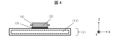
- FIGS. 2 to 4 show cross sections of the second to fourth embodiments of the vapor chamber of the present invention.
- the chamber body (1) used for the vapor chamber according to one aspect of the present invention is a first outer surface, a first inner surface which is the back surface of the first outer surface, a second outer surface, and a second surface which is the back surface of the second outer surface. It has an inner surface and has a sealed space between the first inner surface and the second inner surface.
- the chamber body (1) having the sealed space is not particularly limited as long as it is a material and a structure that prevents the liquid substance (11) described later from leaking to the outside.
- the material is preferably metal, and is particularly preferably copper or aluminum from the viewpoint of excellent thermal conductivity.
- the chamber body is a hollow cylinder formed of a bottomed cylinder forming an outer surface and a second inner surface. From the viewpoint of ease of manufacture, it is more preferable to have a square flat plate and a square bottomed cylinder, respectively.
- a hollow cylindrical chamber body having airtightness can be manufactured by joining the flat plate and the bottomed cylinder to each other by diffusion bonding, brazing, soldering, or other known techniques.
- the entire inner wall surface including the first inner surface and the second inner surface of the chamber body (1) is, for example, . It is preferable that a wick having a porous structure is arranged. Alternatively, a fine structure may be formed by etching or the like.
- the size of the chamber body (1) used for the vapor chamber according to one aspect of the present invention is preferably selected in consideration of the sizes of the semiconductor element (5) and the heat sink (6) described later, for example, 100 mm ⁇ 100 mm. It is possible to use a size such as, but it is not particularly limited.
- the total thickness of the chamber body (1) used for the vapor chamber according to one aspect of the present invention can be in the range of 0.5 to 10.0 mm from the viewpoint of ease of manufacture and handling. However, it is not particularly limited.
- the liquid material (11) used for the vapor chamber according to one aspect of the present invention is enclosed inside the chamber body (1).
- the liquid substance (11) reaches a temperature equal to or higher than the boiling point, it evaporates on the inner wall surface of the chamber body (1), and the gas moves in the hollow portion of the chamber body (1).
- the liquid material (11) reaches a temperature below the boiling point, it condenses and the liquid moves on the inner wall surface. This circulation allows semi-permanent heat transport.
- the type of the liquid substance (11) is not particularly limited, but pure water, alcohol, ammonia and the like can be preferably used. Although it is possible to use one of these or a combination of these, pure water is particularly preferably used from the viewpoint of safety and cost.
- the heat diffusion member (2) used in the vapor chamber according to one aspect of the present invention is arranged on the first outer surface and / or the second outer surface of the chamber body (1), and the first outer surface and / of the chamber body (1). Alternatively, it has a thermal conductivity of 500 W / mK or more in the plane direction orthogonal to the second outer surface. Since the thermal conductivity of the heat diffusion member (2) is 500 W / mK or more, the heat of the semiconductor element (5), which will be described later, is spread in the plane while suppressing the loss due to thermal resistance. The effective area of the vapor chamber can be increased, and the heat transport amount of the vapor chamber according to one aspect of the present invention can be increased.
- the thermal conductivity of the heat diffusion member (2) should be high, more preferably 800 W / mK or more, and particularly preferably 1000 W / mK or more.
- the material of the heat diffusion member (2) used in the vapor chamber according to one aspect of the present invention preferably contains anisotropic graphite from the viewpoint of thermal conductivity.
- Anisotropic graphite is a laminate of a large number of graphite layers and has high thermal conductivity along the crystal orientation plane. In addition, the thermal conductivity is generally low in the direction orthogonal to the crystal orientation plane.
- the method for producing anisotropic graphite is not particularly limited, but it can be produced by cutting a graphite block. Examples of the method for cutting the graphite block include a diamond cutter, a wire saw, and machining. A wire saw is preferable from the viewpoint that it can be easily processed into a rectangular parallelepiped shape.
- anisotropic graphite may be polished or roughened, and known techniques such as sanding, buffing, and blasting can be appropriately used.
- the heat diffusion member (2) has a thermal conductivity of 500 W / mK or more in the plane direction orthogonal to the first outer surface and / or the second outer surface of the chamber body (1).
- the crystal orientation plane of anisotropic graphite is orthogonal to the first outer plane of the chamber body (1) and parallel to the YZ plane.
- the heat diffusion member (2) has a thermal conductivity of 500 W / mK or more in the plane direction of the YZ surface.
- the heat diffusion member (2) when the heat diffusion member (2) is arranged on the first outer surface in a state of being rotated 90 degrees about the Z axis from the state shown in FIGS. 1 and 2, the crystal orientation plane is parallel to the XZ plane. Yes, the heat diffusion member (2) has a thermal conductivity of 500 W / mK or more in the plane direction of the XZ plane.
- the arrangement of the heat diffusing member (2) with respect to the first outer surface and / or the second outer surface is not limited to the above case.
- the heat diffusion member (2) has a first outer surface and / or a second so that the plane direction of the crystal orientation plane of anisotropic graphite is parallel to the plane orthogonal to the first outer plane and / or the second outer plane. It suffices if it is arranged on the outer surface.
- the crystal alignment plane of anisotropic graphite may have a predetermined angle, not parallel to the plane direction orthogonal to the first outer plane and / or the second outer plane.
- the crystal orientation plane when the heat diffusion member (2) is arranged on the first outer surface, the crystal orientation plane may have a predetermined angle with respect to the YZ plane.
- the crystal orientation plane preferably has an angle of ⁇ 10 degrees or less with respect to the YZ plane, and more preferably an angle of ⁇ 5 degrees or less.
- the crystal orientation plane may have an angle of preferably ⁇ 10 degrees or less, more preferably ⁇ 5 degrees or less with respect to the plane orthogonal to the first outer surface and / or the second outer surface. Just do it.
- the graphite block is not particularly limited, and a polymer-decomposed graphite block, a pyrolysis graphite block, an extruded graphite block, a molded graphite block, or the like can be used. From the viewpoint of having high thermal conductivity and excellent thermal transfer performance of anisotropic graphite, polymer-decomposed graphite blocks and pyrolytic graphite blocks are preferable.
- a carbonaceous gas such as methane is introduced into a furnace and heated to about 2000 ° C. with a heater to form fine carbon nuclei.
- the formed carbon nuclei can be deposited in layers on the substrate to obtain a pyrolysis graphite block.
- the graphite block may be produced by laminating a polymer film such as a polyimide resin in multiple layers and then heat-treating the graphite block while pressing the press.
- a multilayer of polymer films which is a starting material, is preheated to a temperature of about 1000 ° C. under reduced pressure or in an inert gas.
- the carbonized block can be graphitized by heat-treating it to a temperature of 2000 ° C. or higher, preferably 2800 ° C. or higher while press-pressurizing it in an inert gas atmosphere to form a good graphite crystal structure. It is possible to obtain a graphite block having excellent thermal conductivity.
- the heat diffusion member (2) used in the vapor chamber according to one aspect of the present invention preferably has a thickness in the range of 0.5 to 10.0 mm.
- the thickness is thinner than 0.5 mm, the effective area of the evaporative portion cannot be sufficiently expanded, and the heat transport amount of the vapor chamber according to one aspect of the present invention does not increase, so that the effect of suppressing the temperature rise of the semiconductor element is obtained. It may not appear.
- the thickness is thicker than 10.0 mm, the thermal resistance of the heat diffusion member (2) itself becomes large, so that the heat transport amount of the vapor chamber according to one aspect of the present invention does not increase, and therefore the temperature of the semiconductor element. The effect of suppressing the rise may not appear.
- the lower limit of the thickness of the heat diffusion member (2) is more preferably 1.0 mm in view of expanding the effective area of the evaporation portion and reducing the thermal resistance of the heat diffusion member (2). Is particularly preferred. Further, the upper limit value is more preferably 5.0 mm, and particularly preferably 3.0 mm.
- the area of the heat diffusion member (2) in the surface direction preferably has an area in the range of 4 to 100% with respect to the area of the first outer surface and / or the second outer surface of the chamber body (1).
- the area is smaller than 4%, the effective area of the evaporating part cannot be sufficiently expanded and the heat transport amount of the vapor chamber according to one aspect of the present invention does not increase, so that the effect of suppressing the temperature rise of the semiconductor element appears. Sometimes not. On the other hand, even if the area is made larger than 100%, the effect of increasing the heat transport amount of the vapor chamber according to one aspect of the present invention according to the area cannot be expected.
- the lower limit is more preferably 8% from the viewpoint of increasing the heat transport amount of the vapor chamber according to one aspect of the present invention and efficiently obtaining the effect of suppressing the temperature rise of the semiconductor element.
- the upper limit value is more preferably 50%.
- the area in the surface direction is an area in the range of 4 to 100% with respect to the area of the first outer surface and / or the second outer surface of the chamber body (1).
- the size is not particularly limited as long as it is present, but the size is preferably in the range of 10 mm ⁇ 10 mm to 100 mm ⁇ 100 mm from the viewpoint of actual use. If it is smaller than 10 mm ⁇ 10 mm, the effective area of the evaporation portion cannot be sufficiently expanded, and it is difficult to obtain the effect of suppressing the temperature rise of the semiconductor element. On the other hand, even if it is larger than 100 mm ⁇ 100 mm, it is difficult to obtain a further effect.
- the lower limit of the heat diffusion member (2) is more preferably 20 mm ⁇ 20 mm. Further, the upper limit is more preferably 75 mm ⁇ 75 mm.
- the heat diffusion member As a first embodiment for efficiently obtaining the effect of expanding the effective area of the evaporating portion and suppressing the temperature rise of the semiconductor element, as shown in FIG. 1, the heat diffusion member
- An example is one in which the (2) and the chamber body (1) are joined via a joining layer (3).
- the bonding layer (3) may contain at least one selected from the group consisting of solder, brazing material, diffusion bonding, and thermally conductive grease. Diffusion bonding is preferable for solder and brazing material from the viewpoint of minimizing the thermal resistance interposed in the bonding layer (3), but solder is particularly preferable from the viewpoint of handling.
- the type of solder is not particularly limited, and solid or paste-like solders can be appropriately used.
- the heat diffusing member (2) may be arranged and joined to the first outer surface and / or the second outer surface of the chamber body (1) in any manner, but may be arranged and joined to one side of the heat diffusing member (2). It is more preferable that the entire surface is arranged so as to be joined to the chamber body (1), and it is particularly preferable that the heat diffusion member (2) is arranged approximately in the central portion of the chamber body (1).
- a coating layer (4) containing either metal or ceramics on at least a part of the surface of the heat diffusion member (2) of FIG. May be possessed.
- the coating layer (4) containing either metal or ceramics on at least a part of the surface damage to the heat diffusion member (2) can be prevented, and the handleability of the vapor chamber according to one aspect of the present invention can be improved. improves. It is preferable that the entire surface facing the semiconductor element is covered, and it is particularly preferable that the entire surface other than the surface facing the bonding layer (3) is covered.
- ⁇ Method of forming the covering layer (4)> As a method for forming the coating layer in the second embodiment of the present invention, known techniques such as plating, sputtering, and thermal spraying, and a method for joining metal or ceramic plates can be appropriately used. When the method of joining metal or ceramic plates is used, these are pre-processed into bottomed shaped parts that can cover the heat diffusion member (2) by using known techniques such as drawing, cutting, and bending. However, a method of joining with the heat diffusion member (2) with a metal-based brazing material is preferable. Further, the bottomed-shaped component may have an offset portion (offset region), and by appropriately providing the offset portion, the arrangement on the chamber main body (1) is stable. Since the metallic brazing material itself has a relatively high thermal conductivity, it is unlikely to generate thermal resistance. The type of the metal brazing material is not particularly limited, but it is preferable to contain silver, copper, and titanium from the viewpoint of maintaining high thermal conductivity.
- the joining method in the case of a metal-based brazing material a known material and a known technique can be used.
- active silver wax when active silver wax is used, the active silver wax having a thickness in the range of 0.005 to 0.05 mm is placed in a vacuum environment of 1 ⁇ 10 -3 Pa, an argon atmosphere, or a reducing atmosphere such as hydrogen. , And heating in a temperature range of 700 to 1000 ° C. for about 10 minutes to 1 hour, and cooling this to room temperature can be used for bonding. Further, in order to improve the bonding state, a weight may be applied during heating.
- the lower limit of the thickness of the coating layer (4) is preferably 0.005 mm, and particularly preferably 0.01 mm.
- the upper limit is preferably 0.5 mm, and particularly preferably 0.3 mm. If it is thinner than 0.005 mm, it is difficult to obtain the effect of preventing the heat diffusion member (2) from being damaged. Further, if it is thicker than 0.5 mm, the heat transport amount of the vapor chamber may decrease because it itself becomes a thermal resistance, which is not preferable.
- the material of the coating layer (4) is not particularly limited as long as it is a metal or ceramics, but it is preferable to use a material having a thermal conductivity of 100 W / mK or more, such as silver, copper, aluminum, and aluminum nitride. If a material having a thermal conductivity of less than 100 W / mK is used, the heat transport amount of the vapor chamber may decrease due to the influence of the thermal resistance of the coating layer, which is not preferable.
- the coating layer (4) may be provided with an offset portion in the surface direction at the surface direction end portion of the heat diffusion member. ..
- the width of the offset portion the lower limit width is preferably 0.5 mm, and the upper limit width is preferably 5 mm. If the width of the offset portion is smaller than 0.5 mm, the offset portion is liable to be damaged and the arrangement may become unstable.
- the offset portion is determined in advance with masking tape on the chamber body (1), and the heat diffusion member (2) is attached.
- a method of forming the coating layer (4) after the arrangement and then peeling off the masking tape can be mentioned.
- a shape that can cover the heat diffusion member (2) and has an offset portion by using known techniques such as drawing, cutting, and bending.
- a metal or ceramic plate is processed in advance, and a metal-based brazing material is bonded to the heat diffusion member (2) in the same manner as in the second embodiment of the vapor chamber of the present invention described above.
- the method of arranging in 1) can be mentioned.
- a coating layer covers both sides of the heat diffusion member, and an offset portion in the surface direction is provided at the end portion in the surface direction. You may be.
- an offset portion By providing such an offset portion, it is possible to suppress the internal stress of the heat diffusion member (2), and there is an advantage that the arrangement on the chamber body (1) is easy to be stable.
- the width of the offset portion 0.5 mm or more is sufficient.
- the heat diffusion member (2) is formed by using known techniques such as drawing, cutting, and bending.
- a metal or ceramic plate is pre-processed into a shape that can be covered and has an offset portion, and a heat diffusion member (2) is made of a metal-based brazing material as in the second embodiment of the vapor chamber of the present invention described above.
- a method of arranging the material joined to the chamber body (1) can be mentioned.
- the heat diffusion member (2) of the vapor chamber according to one aspect of the present invention and the semiconductor element (5) can be joined to form a semiconductor package. Further, a semiconductor package having a heat sink (6) on the surface of the vapor chamber according to one aspect of the present invention on the surface opposite to the side on which the semiconductor element (5) is installed can be obtained.
- the semiconductor package equipped with the vapor chamber according to one aspect of the present invention makes it possible to efficiently suppress the temperature rise of the semiconductor element.
- FIG. 5 shows a first embodiment of a semiconductor package on which the vapor chamber of the first embodiment of the present invention is mounted.
- FIG. 6 shows a cross section of a second embodiment of a semiconductor package on which the vapor chamber of the third embodiment of the present invention is mounted.
- the semiconductor element (5) used in the semiconductor package according to one aspect of the present invention is not particularly limited, and examples thereof include a CPU, a GPU, an FPGA, a transistor, a diode, and a memory.
- the heat sink (6) used in the semiconductor package according to one aspect of the present invention is not particularly limited, and known ones such as parallel comb fins, pin fins, corrugated fins, water-cooled heat sinks, and Pelche modules can be used.
- a motor fan may be used in combination to promote cooling.
- the semiconductor package on which the vapor chamber of the first embodiment of the present invention is mounted as the first embodiment for expanding the effective area of the evaporating portion and efficiently obtaining the effect of suppressing the temperature rise of the semiconductor element.
- the semiconductor element (5), the heat diffusion member (2), the chamber body (1), and the heat sink (6) are configured in this order.
- known materials such as solder, heat conductive grease, and heat conductive sheet can be used, but from the viewpoint of minimizing the thermal resistance. , Handa is preferred.
- the type of solder is not particularly limited, and solid or paste-like solders can be appropriately used.
- solder As a method for joining the chamber body (1) and the heat sink (6), known materials such as solder, brazing material, diffusion bonding, heat conductive grease, and heat conductive sheet can be used, but thermal resistance. Solder, brazing material, and diffusion bonding are preferable from the viewpoint of reducing the pressure as much as possible, and solder is particularly preferable from the viewpoint of handling.
- the type of solder is not particularly limited, and solid or paste-like solders can be appropriately used.
- the second embodiment for expanding the effective area of the evaporating part (7) and efficiently obtaining the effect of suppressing the temperature rise of the semiconductor element.
- the semiconductor element (5), the heat diffusion member (2) provided with the coating layer (4) on the semiconductor element (5) side, and the chamber body (1). ), And the heat sink (6) are configured in this order.
- As a method for forming the coating layer (4) it is possible to use the same method as in the second to fourth embodiments of the vapor chamber of the present invention.
- the method of joining the heat diffusion member (2) and the semiconductor element (5) and the method of joining the chamber body (1) and the heat sink (6) are the same as those in the first embodiment of the semiconductor package described above. It is possible to use the method of.
- the area of the evaporation portion (7) is clearly larger than the area of the semiconductor element (5), and the area is clearly larger than that of the semiconductor element (5). Since the area of the condensed portion (8) is also sufficiently large, it is possible to efficiently suppress the temperature rise of the semiconductor element.
- Examples of the present invention will be described below.
- Examples 1 to 9 and Comparative Examples 2 to 4 are located at the center of the surface of the heat diffusion member opposite to the surface of the chamber body, and Comparative Example 1 is located at the center of the first outer surface of the chamber body.
- a semiconductor element (10 mm ⁇ 10 mm) is bonded via G-775 (manufactured by Shin-Etsu Chemical Industry Co., Ltd.), and a water-cooled heat sink (water temperature 25 ° C.) is applied to the entire second outer surface of the chamber body via the heat conductive grease. ) was joined to manufacture a semiconductor package. A heat of 100 W was generated in the semiconductor element, and the temperature of the semiconductor element at that time was measured using a thermocouple.
- the effect of suppressing the temperature rise is "A”, if it is 90 ° C or higher and lower than 100 ° C, it is “B”, if it is 100 ° C or higher and lower than 110 ° C, it is “C”, and 110 ° C or higher. If it is, it is set to "D”, and when it is "A” or "B", it is judged that the heat transport amount of the vapor chamber is high and the temperature rise of the semiconductor element in the semiconductor package can be suppressed.
- the graphite block used as a raw material for anisotropic graphite A used for the heat diffusion member was manufactured as follows. After laminating 20000 pieces of polyimide film manufactured by Kaneka Corporation with a thickness of 100 mm x 100 mm x 12.5 ⁇ m, a graphite block is heat-treated to 2200 ° C. under an argon atmosphere while pressing and pressing at a pressure of 40 kg / cm 2 . (90 mm ⁇ 90 mm, thickness 100 mm) was produced. The thermal conductivity of the obtained graphite block in the direction parallel to the crystal orientation plane was 600 W / mK, and the thermal conductivity in the direction perpendicular to the crystal orientation plane was 5 W / mK.
- the graphite block used as a raw material for anisotropic graphite B used for the heat diffusion member was manufactured as follows. After laminating 20000 sheets of polyimide film manufactured by Kaneka Corporation with a thickness of 100 mm x 100 mm x 12.5 ⁇ m, a graphite block is heat-treated to 2900 ° C. under an argon atmosphere while pressing and pressing at a pressure of 40 kg / cm 2 . (90 mm ⁇ 90 mm, thickness 100 mm) was produced. The thermal conductivity of the obtained graphite block in the direction parallel to the crystal orientation plane was 1500 W / mK, and the thermal conductivity in the direction perpendicular to the crystal orientation plane was 5 W / mK.
- the chamber body was manufactured as follows. Using a copper flat plate having a first outer surface and a copper bottomed cylinder having a second outer surface, a square hollow cylinder having a size of 100 mm ⁇ 100 mm and a thickness of 5 mm was prepared. A wick with a porous structure was placed on the entire inner wall surface, and the liquid material was pure water.
- Example 1 The graphite block obtained in Production Example 1 was cut with a wire saw (model number: WSD-K2, manufactured by Takatori Co., Ltd.) to obtain anisotropic graphite A having a flat surface size of 30 mm ⁇ 30 mm and a thickness of 1.5 mm. ..
- the anisotropic graphite A had crystal orientation planes arranged along the thickness direction and had a thermal conductivity of 600 W / mK.
- a heat conductive grease model number: G-775, manufactured by Shin-Etsu Chemical Co., Ltd.
- the temperature of the semiconductor element was evaluated using the vapor chamber, the temperature of the semiconductor element was 95 ° C., and the evaluation was "B".
- Example 2 The graphite block obtained in Production Example 2 is cut with a wire saw (model number: WSD-K2, manufactured by Takatori Co., Ltd.), and as a heat diffusion member, anisotropic graphite having a flat surface size of 30 mm ⁇ 30 mm and a thickness of 1.5 mm is used. B was obtained. The anisotropic graphite B had crystal orientation planes arranged along the thickness direction and had a thermal conductivity of 1500 W / mK. Electroplating is performed with masking tape (model number: 851A, manufactured by 3M) attached to the entire surface of the flat side of the heat diffusion member to form a 0.01 mm thick Cu coating layer on the surface, and then masking is performed.
- masking tape model number: 851A, manufactured by 3M
- the tape was removed to produce a heat diffusion member having a Cu coating layer formed on only one side.
- the graphite exposed surface of the heat diffusion member is the first chamber body via a heat conductive grease (model number: G-775, manufactured by Shin-Etsu Chemical Co., Ltd.) in the center of the first outer surface of the chamber body obtained in Production Example 3.
- a vapor chamber as shown in FIG. 2 was manufactured by arranging it so as to face the outer surface.
- the temperature of the semiconductor element was evaluated using the vapor chamber, the temperature of the semiconductor element was 78 ° C., and the evaluation was "A".
- Example 3 A clad material in which an active silver wax with a thickness of 0.013 mm (model number: TKC-661, manufactured by Tanaka Kikinzoku Kogyo Co., Ltd.) is pre-formed on a copper plate with a thickness of 0.2 mm is prepared and drawn by using a mold. , A bottomed part having an inner dimension of 30 mm ⁇ 30 mm ⁇ 1.5 mm and a width of an offset portion at the end in the plane direction of 1 mm was manufactured. Anisotropic graphite B, which is a heat diffusion member obtained in the same manner as in Example 2, was loaded into the bottomed shape component and heat-treated at 780 ° C. for 30 minutes under a vacuum of 1 ⁇ 10 -3 Pa.
- the two were uniformly bonded to produce a heat-diffusing member in which a Cu coating layer having a thickness of 0.2 mm was formed on only one side.
- the graphite exposed surface of the heat diffusion member is the first chamber body via a heat conductive grease (model number: G-775, manufactured by Shin-Etsu Chemical Co., Ltd.) in the center of the first outer surface of the chamber body obtained in Production Example 3.
- a vapor chamber as shown in FIG. 3 was manufactured by arranging it so as to face the outer surface.
- the temperature of the semiconductor element was evaluated using the vapor chamber, the temperature of the semiconductor element was 83 ° C., and the evaluation was "A".
- Example 4 The figure is the same as in Example 3 except that the thickness of the anisotropic graphite B is 3.0 mm, the thickness of the copper plate is 0.3 mm, and the inner dimensions of the bottomed portion are 30 mm ⁇ 30 mm ⁇ 3.0 mm.
- a vapor chamber as shown in 3 was manufactured. When the temperature of the semiconductor element was evaluated using the vapor chamber, the temperature of the semiconductor element was 82 ° C., and the evaluation was "A".
- Example 5 The figure is the same as in Example 3 except that the planar size of the anisotropic graphite B is 98 mm ⁇ 98 mm, the thickness is 5.0 mm, and the inner dimensions of the bottomed shape component are 100 mm ⁇ 100 mm ⁇ 5.0 mm.
- a vapor chamber as shown in 3 was manufactured. When the temperature of the semiconductor element was evaluated using the vapor chamber, the temperature of the semiconductor element was 88 ° C., and the evaluation was "A".
- Example 6 The aluminum nitride block was cut so that the inner dimensions were 30 mm ⁇ 30 mm ⁇ 1.5 mm and the width of the offset portion was 1 mm, and a bottomed shape part was manufactured.
- An active silver wax foil (model number: TKC-661, manufactured by Tanaka Kikinzoku Kogyo Co., Ltd.) having a thickness of 0.013 mm and anisotropic graphite B, which is a heat diffusion member obtained in the same manner as in Example 2, are applied to the bottomed shape component. In the state of being loaded in order, heat treatment was performed at 780 ° C.
- a diffuser member was manufactured.
- the graphite exposed surface of the heat diffusion member is the first chamber body via a heat conductive grease (model number: G-775, manufactured by Shin-Etsu Chemical Co., Ltd.) in the center of the first outer surface of the chamber body obtained in Production Example 3.
- a vapor chamber as shown in FIG. 3 was manufactured by arranging it so as to face the outer surface.
- the temperature of the semiconductor element was evaluated using the vapor chamber, the temperature of the semiconductor element was 91 ° C., and the evaluation was "B".
- Example 7 The figure is the same as in Example 3 except that the planar size of the anisotropic graphite B is 20 mm ⁇ 20 mm, the thickness is 1.0 mm, and the inner dimensions of the bottomed shape component are 20 mm ⁇ 20 mm ⁇ 1.0 mm.
- a vapor chamber as shown in 3 was manufactured. When the temperature of the semiconductor element was evaluated using the vapor chamber, the temperature of the semiconductor element was 94 ° C., and the evaluation was "B".
- Example 8 A clad material in which an active silver wax with a thickness of 0.013 mm (model number: TKC-661, manufactured by Tanaka Kikinzoku Kogyo Co., Ltd.) is pre-formed on a copper plate with a thickness of 0.2 mm is prepared and drawn by using a mold. , A bottomed part having an inner dimension of 70 mm ⁇ 70 mm ⁇ 1.5 mm and an offset portion width of 1 mm was manufactured. With the two bottomed parts facing each other and loaded with anisotropic graphite B, which is the heat diffusion member, heat treatment is performed at 780 ° C. for 30 minutes under a vacuum of 1 ⁇ 10 -3 Pa to make both uniform.
- anisotropic graphite B which is the heat diffusion member
- a heat diffusion member having a 0.2 mm thick Cu coating layer formed on the surface thereof was manufactured.
- the main surface (70 mm ⁇ 70 mm surface) of the heat diffusion member is interposed at the center of the first outer surface of the chamber body obtained in Production Example 3 via a heat conductive grease (model number: G-775, manufactured by Shin-Etsu Chemical Co., Ltd.).
- a heat conductive grease model number: G-775, manufactured by Shin-Etsu Chemical Co., Ltd.
- the temperature of the semiconductor element was 82 ° C., and the evaluation was "A".
- Example 9 A vapor chamber as shown in FIG. 1 was manufactured in the same manner as in Example 1 except that anisotropic graphite B was used as the heat diffusion member.
- the temperature of the semiconductor element was evaluated using the vapor chamber, the temperature of the semiconductor element was 77 ° C., and the evaluation was "A".
- Example 2 A vapor chamber as shown in FIG. 1 was manufactured in the same manner as in Example 1 except that a pure copper material was used as the heat diffusion member.
- the temperature of the semiconductor element was 103 ° C., and the evaluation was "C".
- Comparative Example 3 A vapor chamber as shown in FIG. 1 was manufactured in the same manner as in Comparative Example 2 except that a heat diffusion member having a flat surface size of 100 mm ⁇ 100 mm was used.
- the temperature of the semiconductor element was 100 ° C., and the evaluation was "C".
- Comparative Example 4 A vapor chamber as shown in FIG. 1 was manufactured in the same manner as in Comparative Example 3 except that a heat diffusion member having a thickness of 5.0 mm was used.
- the temperature of the semiconductor element was 110 ° C., and the evaluation was "D".
- Table 1 summarizes the configurations and evaluation results of Examples and Comparative Examples. From Table 1, it is clear that the vapor chamber in which the heat diffusion member having a thermal conductivity of 500 W / mK or more is arranged is effective in suppressing the temperature rise of the semiconductor element.
- the vapor chamber according to one aspect of the present invention relates to the following.
- the chamber body has a first outer surface, a first inner surface which is a back surface of the first outer surface, a second outer surface, and a second inner surface which is a back surface of the second outer surface.
- the sealed space is provided between the first inner surface and the second inner surface.
- the liquid material is enclosed in the sealed space, and the heat diffusion member is provided on the first outer surface and / or the second outer surface of the chamber body.
- the heat diffusion member is a vapor chamber having a thermal conductivity of 500 W / mK or more in a plane direction orthogonal to the first outer surface or the second outer surface of the chamber body.
- VIII The vapor chamber according to (VI) or (VII), wherein the coating layer is provided with an offset region having a width of 0.5 mm or more in the surface direction at the surface direction end portion of the heat diffusion member.
- IX The vapor chamber according to any one of (I) to (VIII), wherein the heat diffusion member has a thickness of 0.5 to 10.0 mm.
- (X) The vapor chamber according to any one of (I) to (IX), wherein the area of the heat diffusion member in the surface direction is 4 to 100% of the area of the first outer surface or the second outer surface of the chamber body. ..
- (XI) A semiconductor package having a semiconductor element and the vapor chamber according to any one of (I) to (X), to which the heat diffusion member and the semiconductor element are bonded.
- (XII) The semiconductor package according to (XI), which has a heat sink on a surface of the chamber body opposite to the surface on the heat diffusion member side.
- the vapor chamber according to one aspect of the present invention is suitable for providing a semiconductor package capable of suppressing a temperature rise of a semiconductor element.
- Chamber body (11) Liquid material (2) Heat diffusion member (3) Bonding layer (4) Coating layer (5) Semiconductor element (6) Heat sink (7) Evaporation part (8) Condensation part
Landscapes
- Cooling Or The Like Of Semiconductors Or Solid State Devices (AREA)
Priority Applications (3)
| Application Number | Priority Date | Filing Date | Title |
|---|---|---|---|
| JP2022546960A JP7731361B2 (ja) | 2020-09-02 | 2021-09-02 | ベイパーチャンバー、及び、これを搭載する半導体パッケージ |
| CN202180053897.2A CN116018678A (zh) | 2020-09-02 | 2021-09-02 | 导热板、以及安装有此导热板的半导体封装体 |
| US18/176,210 US20230207425A1 (en) | 2020-09-02 | 2023-02-28 | Vapor chamber and semiconductor package having same mounted thereon |
Applications Claiming Priority (2)
| Application Number | Priority Date | Filing Date | Title |
|---|---|---|---|
| JP2020-147802 | 2020-09-02 | ||
| JP2020147802 | 2020-09-02 |
Related Child Applications (1)
| Application Number | Title | Priority Date | Filing Date |
|---|---|---|---|
| US18/176,210 Continuation US20230207425A1 (en) | 2020-09-02 | 2023-02-28 | Vapor chamber and semiconductor package having same mounted thereon |
Publications (1)
| Publication Number | Publication Date |
|---|---|
| WO2022050337A1 true WO2022050337A1 (ja) | 2022-03-10 |
Family
ID=80491082
Family Applications (1)
| Application Number | Title | Priority Date | Filing Date |
|---|---|---|---|
| PCT/JP2021/032236 Ceased WO2022050337A1 (ja) | 2020-09-02 | 2021-09-02 | ベイパーチャンバー、及び、これを搭載する半導体パッケージ |
Country Status (4)
| Country | Link |
|---|---|
| US (1) | US20230207425A1 (https=) |
| JP (1) | JP7731361B2 (https=) |
| CN (1) | CN116018678A (https=) |
| WO (1) | WO2022050337A1 (https=) |
Cited By (1)
| Publication number | Priority date | Publication date | Assignee | Title |
|---|---|---|---|---|
| WO2025192282A1 (ja) * | 2024-03-15 | 2025-09-18 | 日本発條株式会社 | 積層体 |
Citations (8)
| Publication number | Priority date | Publication date | Assignee | Title |
|---|---|---|---|---|
| JP2003124665A (ja) * | 2001-10-11 | 2003-04-25 | Fujikura Ltd | 電子装置用放熱構造 |
| JP2008522129A (ja) * | 2004-12-01 | 2008-06-26 | コンバージェンス テクノロジーズ リミテッド | 沸騰促進マルチウィック構造物を備えた蒸気チャンバー |
| JP2015050323A (ja) * | 2013-09-02 | 2015-03-16 | 株式会社フジクラ | 半導体パッケージの複合冷却構造 |
| WO2016098890A1 (ja) * | 2014-12-18 | 2016-06-23 | 株式会社カネカ | グラファイト積層体、グラファイト積層体の製造方法、熱輸送用構造物およびロッド状の熱輸送体 |
| JP2017216350A (ja) * | 2016-05-31 | 2017-12-07 | 日産自動車株式会社 | 半導体装置 |
| WO2019102665A1 (ja) * | 2017-11-21 | 2019-05-31 | ローム株式会社 | 半導体装置、パワーモジュールおよび電源装置 |
| JP2019140332A (ja) * | 2018-02-14 | 2019-08-22 | トヨタ自動車株式会社 | 半導体装置 |
| WO2019188614A1 (ja) * | 2018-03-28 | 2019-10-03 | 株式会社カネカ | 半導体パッケージ |
-
2021
- 2021-09-02 WO PCT/JP2021/032236 patent/WO2022050337A1/ja not_active Ceased
- 2021-09-02 JP JP2022546960A patent/JP7731361B2/ja active Active
- 2021-09-02 CN CN202180053897.2A patent/CN116018678A/zh active Pending
-
2023
- 2023-02-28 US US18/176,210 patent/US20230207425A1/en active Pending
Patent Citations (8)
| Publication number | Priority date | Publication date | Assignee | Title |
|---|---|---|---|---|
| JP2003124665A (ja) * | 2001-10-11 | 2003-04-25 | Fujikura Ltd | 電子装置用放熱構造 |
| JP2008522129A (ja) * | 2004-12-01 | 2008-06-26 | コンバージェンス テクノロジーズ リミテッド | 沸騰促進マルチウィック構造物を備えた蒸気チャンバー |
| JP2015050323A (ja) * | 2013-09-02 | 2015-03-16 | 株式会社フジクラ | 半導体パッケージの複合冷却構造 |
| WO2016098890A1 (ja) * | 2014-12-18 | 2016-06-23 | 株式会社カネカ | グラファイト積層体、グラファイト積層体の製造方法、熱輸送用構造物およびロッド状の熱輸送体 |
| JP2017216350A (ja) * | 2016-05-31 | 2017-12-07 | 日産自動車株式会社 | 半導体装置 |
| WO2019102665A1 (ja) * | 2017-11-21 | 2019-05-31 | ローム株式会社 | 半導体装置、パワーモジュールおよび電源装置 |
| JP2019140332A (ja) * | 2018-02-14 | 2019-08-22 | トヨタ自動車株式会社 | 半導体装置 |
| WO2019188614A1 (ja) * | 2018-03-28 | 2019-10-03 | 株式会社カネカ | 半導体パッケージ |
Cited By (1)
| Publication number | Priority date | Publication date | Assignee | Title |
|---|---|---|---|---|
| WO2025192282A1 (ja) * | 2024-03-15 | 2025-09-18 | 日本発條株式会社 | 積層体 |
Also Published As
| Publication number | Publication date |
|---|---|
| US20230207425A1 (en) | 2023-06-29 |
| JPWO2022050337A1 (https=) | 2022-03-10 |
| CN116018678A (zh) | 2023-04-25 |
| JP7731361B2 (ja) | 2025-08-29 |
Similar Documents
| Publication | Publication Date | Title |
|---|---|---|
| CN102575914B (zh) | 各向异性热传导元件及其制造方法 | |
| CN210108104U (zh) | 一种均温板 | |
| CN110192273A (zh) | 用于在热接地平面中散布高热通量的方法和设备 | |
| JPH0364097A (ja) | ヒート・シンク基板 | |
| CN112839799B (zh) | 带金属层的碳质构件及导热板 | |
| JP2021100006A (ja) | 半導体パッケージ | |
| CN111725144A (zh) | 基于气液相变的高温电子封装基板材料器件及其制备方法 | |
| CN117870426B (zh) | 一种带有激光烧结吸液芯结构的均热板及其制备方法 | |
| KR20220165595A (ko) | 복합재료 및 방열부품 | |
| WO2022050337A1 (ja) | ベイパーチャンバー、及び、これを搭載する半導体パッケージ | |
| JP2005077052A (ja) | 平面型ヒートパイプ | |
| JP2022003656A (ja) | 半導体パッケージ | |
| CN116157258B (zh) | 复合材料、散热器和半导体封装 | |
| CN110944493A (zh) | 一种基于气液相变的金属基复合材料器件及其制备方法 | |
| CN114446903B (zh) | 封装器件、封装模组和电子设备 | |
| JP6040570B2 (ja) | 熱交換器 | |
| JP7133916B2 (ja) | 放熱部材、放熱構造及び電子機器 | |
| CN115682810B (zh) | 石墨烯金属复合散热翅片、散热器、制备方法 | |
| KR102884605B1 (ko) | 복합재료 및 이 복합재료를 포함하는 방열부품 | |
| CN112840751A (zh) | 用于电路板的传导冷却 | |
| CN113075987A (zh) | 具有平板热管和冷却液板复合结构的散热器及其制作方法 | |
| CN112781418A (zh) | 热传导部件 | |
| CN111386601A (zh) | 绝缘基板和散热装置 | |
| TWI823668B (zh) | 兩相浸沒式複合型散熱裝置 | |
| US20250311160A1 (en) | Heat pipe cooling |
Legal Events
| Date | Code | Title | Description |
|---|---|---|---|
| 121 | Ep: the epo has been informed by wipo that ep was designated in this application |
Ref document number: 21864392 Country of ref document: EP Kind code of ref document: A1 |
|
| ENP | Entry into the national phase |
Ref document number: 2022546960 Country of ref document: JP Kind code of ref document: A |
|
| NENP | Non-entry into the national phase |
Ref country code: DE |
|
| 122 | Ep: pct application non-entry in european phase |
Ref document number: 21864392 Country of ref document: EP Kind code of ref document: A1 |