WO2022050337A1 - ベイパーチャンバー、及び、これを搭載する半導体パッケージ - Google Patents
ベイパーチャンバー、及び、これを搭載する半導体パッケージ Download PDFInfo
- Publication number
- WO2022050337A1 WO2022050337A1 PCT/JP2021/032236 JP2021032236W WO2022050337A1 WO 2022050337 A1 WO2022050337 A1 WO 2022050337A1 JP 2021032236 W JP2021032236 W JP 2021032236W WO 2022050337 A1 WO2022050337 A1 WO 2022050337A1
- Authority
- WO
- WIPO (PCT)
- Prior art keywords
- vapor chamber
- diffusion member
- heat diffusion
- heat
- chamber body
- Prior art date
Links
- 239000004065 semiconductor Substances 0.000 title claims abstract description 105
- 238000009792 diffusion process Methods 0.000 claims abstract description 102
- 239000007788 liquid Substances 0.000 claims abstract description 11
- 239000000126 substance Substances 0.000 claims abstract description 10
- OKTJSMMVPCPJKN-UHFFFAOYSA-N Carbon Chemical compound [C] OKTJSMMVPCPJKN-UHFFFAOYSA-N 0.000 claims description 61
- 229910002804 graphite Inorganic materials 0.000 claims description 56
- 239000010439 graphite Substances 0.000 claims description 56
- 239000011247 coating layer Substances 0.000 claims description 23
- 229910052751 metal Inorganic materials 0.000 claims description 21
- 239000002184 metal Substances 0.000 claims description 21
- 239000013078 crystal Substances 0.000 claims description 20
- 229910000679 solder Inorganic materials 0.000 claims description 15
- 238000005219 brazing Methods 0.000 claims description 14
- 239000011344 liquid material Substances 0.000 claims description 14
- 239000010410 layer Substances 0.000 claims description 12
- 239000000919 ceramic Substances 0.000 claims description 11
- 239000004519 grease Substances 0.000 claims description 11
- 239000000945 filler Substances 0.000 claims 1
- 238000000034 method Methods 0.000 description 35
- 239000000463 material Substances 0.000 description 25
- 238000004519 manufacturing process Methods 0.000 description 17
- 238000011156 evaluation Methods 0.000 description 15
- 238000001704 evaporation Methods 0.000 description 14
- 239000010949 copper Substances 0.000 description 13
- 230000000694 effects Effects 0.000 description 13
- 238000005304 joining Methods 0.000 description 12
- RYGMFSIKBFXOCR-UHFFFAOYSA-N Copper Chemical compound [Cu] RYGMFSIKBFXOCR-UHFFFAOYSA-N 0.000 description 9
- 230000000052 comparative effect Effects 0.000 description 9
- 229910052802 copper Inorganic materials 0.000 description 9
- 230000008020 evaporation Effects 0.000 description 9
- BQCADISMDOOEFD-UHFFFAOYSA-N Silver Chemical compound [Ag] BQCADISMDOOEFD-UHFFFAOYSA-N 0.000 description 7
- 238000005520 cutting process Methods 0.000 description 7
- 229910052709 silver Inorganic materials 0.000 description 7
- 239000004332 silver Substances 0.000 description 7
- 238000009833 condensation Methods 0.000 description 5
- 230000005494 condensation Effects 0.000 description 5
- 238000003825 pressing Methods 0.000 description 5
- 230000007423 decrease Effects 0.000 description 4
- 238000010438 heat treatment Methods 0.000 description 4
- 230000000873 masking effect Effects 0.000 description 4
- XLYOFNOQVPJJNP-UHFFFAOYSA-N water Substances O XLYOFNOQVPJJNP-UHFFFAOYSA-N 0.000 description 4
- 239000012300 argon atmosphere Substances 0.000 description 3
- 238000005452 bending Methods 0.000 description 3
- 238000001816 cooling Methods 0.000 description 3
- PMHQVHHXPFUNSP-UHFFFAOYSA-M copper(1+);methylsulfanylmethane;bromide Chemical compound Br[Cu].CSC PMHQVHHXPFUNSP-UHFFFAOYSA-M 0.000 description 3
- 238000010030 laminating Methods 0.000 description 3
- 229920001721 polyimide Polymers 0.000 description 3
- 229920006254 polymer film Polymers 0.000 description 3
- 239000007787 solid Substances 0.000 description 3
- 239000000758 substrate Substances 0.000 description 3
- QGZKDVFQNNGYKY-UHFFFAOYSA-N Ammonia Chemical compound N QGZKDVFQNNGYKY-UHFFFAOYSA-N 0.000 description 2
- 229910052782 aluminium Inorganic materials 0.000 description 2
- XAGFODPZIPBFFR-UHFFFAOYSA-N aluminium Chemical compound [Al] XAGFODPZIPBFFR-UHFFFAOYSA-N 0.000 description 2
- 239000012298 atmosphere Substances 0.000 description 2
- 238000009835 boiling Methods 0.000 description 2
- 229910052799 carbon Inorganic materials 0.000 description 2
- 239000007789 gas Substances 0.000 description 2
- 239000011261 inert gas Substances 0.000 description 2
- 238000002347 injection Methods 0.000 description 2
- 239000007924 injection Substances 0.000 description 2
- VNWKTOKETHGBQD-UHFFFAOYSA-N methane Chemical compound C VNWKTOKETHGBQD-UHFFFAOYSA-N 0.000 description 2
- 238000007747 plating Methods 0.000 description 2
- 238000000197 pyrolysis Methods 0.000 description 2
- 239000002994 raw material Substances 0.000 description 2
- 238000007751 thermal spraying Methods 0.000 description 2
- LFQSCWFLJHTTHZ-UHFFFAOYSA-N Ethanol Chemical compound CCO LFQSCWFLJHTTHZ-UHFFFAOYSA-N 0.000 description 1
- UFHFLCQGNIYNRP-UHFFFAOYSA-N Hydrogen Chemical compound [H][H] UFHFLCQGNIYNRP-UHFFFAOYSA-N 0.000 description 1
- RTAQQCXQSZGOHL-UHFFFAOYSA-N Titanium Chemical compound [Ti] RTAQQCXQSZGOHL-UHFFFAOYSA-N 0.000 description 1
- 229910021529 ammonia Inorganic materials 0.000 description 1
- 238000005422 blasting Methods 0.000 description 1
- 229910003460 diamond Inorganic materials 0.000 description 1
- 239000010432 diamond Substances 0.000 description 1
- 238000009713 electroplating Methods 0.000 description 1
- 238000005530 etching Methods 0.000 description 1
- 239000011888 foil Substances 0.000 description 1
- 239000007770 graphite material Substances 0.000 description 1
- 239000001257 hydrogen Substances 0.000 description 1
- 229910052739 hydrogen Inorganic materials 0.000 description 1
- 238000003754 machining Methods 0.000 description 1
- 238000012986 modification Methods 0.000 description 1
- 230000004048 modification Effects 0.000 description 1
- 239000009719 polyimide resin Substances 0.000 description 1
- 238000005476 soldering Methods 0.000 description 1
- 238000004544 sputter deposition Methods 0.000 description 1
- 239000007858 starting material Substances 0.000 description 1
- 239000010936 titanium Substances 0.000 description 1
- 229910052719 titanium Inorganic materials 0.000 description 1
- 229910052724 xenon Inorganic materials 0.000 description 1
- FHNFHKCVQCLJFQ-UHFFFAOYSA-N xenon atom Chemical compound [Xe] FHNFHKCVQCLJFQ-UHFFFAOYSA-N 0.000 description 1
Images


Classifications
-
- H—ELECTRICITY
- H01—ELECTRIC ELEMENTS
- H01L—SEMICONDUCTOR DEVICES NOT COVERED BY CLASS H10
- H01L23/00—Details of semiconductor or other solid state devices
- H01L23/34—Arrangements for cooling, heating, ventilating or temperature compensation ; Temperature sensing arrangements
- H01L23/42—Fillings or auxiliary members in containers or encapsulations selected or arranged to facilitate heating or cooling
- H01L23/427—Cooling by change of state, e.g. use of heat pipes
-
- H—ELECTRICITY
- H01—ELECTRIC ELEMENTS
- H01L—SEMICONDUCTOR DEVICES NOT COVERED BY CLASS H10
- H01L21/00—Processes or apparatus adapted for the manufacture or treatment of semiconductor or solid state devices or of parts thereof
- H01L21/02—Manufacture or treatment of semiconductor devices or of parts thereof
- H01L21/04—Manufacture or treatment of semiconductor devices or of parts thereof the devices having potential barriers, e.g. a PN junction, depletion layer or carrier concentration layer
- H01L21/48—Manufacture or treatment of parts, e.g. containers, prior to assembly of the devices, using processes not provided for in a single one of the subgroups H01L21/06 - H01L21/326
- H01L21/4814—Conductive parts
- H01L21/4871—Bases, plates or heatsinks
- H01L21/4882—Assembly of heatsink parts
-
- H—ELECTRICITY
- H01—ELECTRIC ELEMENTS
- H01L—SEMICONDUCTOR DEVICES NOT COVERED BY CLASS H10
- H01L23/00—Details of semiconductor or other solid state devices
- H01L23/34—Arrangements for cooling, heating, ventilating or temperature compensation ; Temperature sensing arrangements
- H01L23/36—Selection of materials, or shaping, to facilitate cooling or heating, e.g. heatsinks
- H01L23/373—Cooling facilitated by selection of materials for the device or materials for thermal expansion adaptation, e.g. carbon
- H01L23/3736—Metallic materials
-
- H—ELECTRICITY
- H01—ELECTRIC ELEMENTS
- H01L—SEMICONDUCTOR DEVICES NOT COVERED BY CLASS H10
- H01L23/00—Details of semiconductor or other solid state devices
- H01L23/34—Arrangements for cooling, heating, ventilating or temperature compensation ; Temperature sensing arrangements
- H01L23/46—Arrangements for cooling, heating, ventilating or temperature compensation ; Temperature sensing arrangements involving the transfer of heat by flowing fluids
- H01L23/473—Arrangements for cooling, heating, ventilating or temperature compensation ; Temperature sensing arrangements involving the transfer of heat by flowing fluids by flowing liquids
Definitions
- the present invention relates to a vapor chamber having a heat diffusion member.
- a vapor chamber may be used as an example of a means for suppressing a temperature rise of a semiconductor package.
- it is necessary to smoothly evaporate and condense the liquid material enclosed in the chamber body of the vapor chamber. If the balance between evaporation and condensation is greatly lost, a decrease in heat transport called dryout occurs, so it is necessary to consider the effective area of the evaporation part and the condensation part.
- Patent Document 1 As a vapor chamber with improved heat transport capacity, for example, in Patent Document 1, a large number of fins are provided inside the chamber body of the vapor chamber, and the fins are connected to the upper plate or the lower plate to reduce the flow rate of the liquid material. It is disclosed to increase and increase heat transport. Further, Patent Document 2 discloses that the vapor chamber and the substrate are connected via a heat conductive portion such as metal, and the heat accumulated in the vapor chamber is transferred to the substrate side.
- a heat conductive portion such as metal
- One aspect of the present invention is to provide a vapor chamber capable of suppressing a temperature rise of a semiconductor element by efficiently transporting heat generated from the semiconductor element, and a semiconductor package on which the vapor chamber is mounted. And.
- the present inventors have found that arranging the heat diffusion member on the surface of the chamber body of the vapor chamber is effective in improving the substantially effective area of the evaporating portion, and the vapor chamber It has been found that the temperature rise of the semiconductor element can be suppressed by increasing the heat transport amount, and the present invention has been completed.
- the vapor chamber according to one aspect of the present invention relates to the following.
- the chamber body has a first outer surface, a first inner surface which is a back surface of the first outer surface, a second outer surface, and a second inner surface which is a back surface of the second outer surface.
- the sealed space is provided between the first inner surface and the second inner surface.
- the liquid material is enclosed in the sealed space, and the heat diffusion member is provided on the first outer surface and / or the second outer surface of the chamber body.
- the heat diffusion member is a vapor chamber having a thermal conductivity of 500 W / mK or more in a plane direction orthogonal to the first outer surface or the second outer surface of the chamber body.
- a vapor chamber capable of increasing the heat transport amount. Further, by using the vapor chamber according to one aspect of the present invention, it is possible to provide a semiconductor package capable of suppressing a temperature rise of a semiconductor element.
- the first embodiment of the vapor chamber of the present invention Cross section of the second embodiment of the vapor chamber of the present invention
- Cross section of the third embodiment of the vapor chamber of the present invention
- Cross section of the fourth embodiment of the vapor chamber of the present invention The first embodiment of the semiconductor package in which the vapor chamber of the first embodiment is mounted.
- the vapor chamber according to one aspect of the present invention is a vapor chamber provided with a chamber main body (1) having a sealed space inside, a liquid substance (11) enclosed in the chamber main body, and a heat diffusion member (2). ..
- the chamber body has a first outer surface, a first inner surface which is the back surface of the first outer surface, a second outer surface, and a second inner surface which is the back surface of the second outer surface.
- the sealed space is provided between the first inner surface and the second inner surface, and the liquid substance (11) is sealed in the sealed space.
- the heat diffusion member (2) is provided on the first outer surface and / or the second outer surface of the chamber body (1).
- the heat diffusion member (2) has a thermal conductivity of 500 W / mK or more in a plane direction orthogonal to the first outer surface or the second outer surface of the chamber body (1).
- the "plane direction orthogonal to the first outer surface or the second outer surface” means the “plane direction in the first outer surface or the plane orthogonal to the second outer surface”.
- Thermal conductivity (W / mK) is the amount of heat that flows through 1 m 2 of a plate when there is a temperature difference of 1 ° C. between both sides of a plate with a thickness of 1 m.
- the thermal conductivity in such a plane direction is expressed by the thermal diffusivity in the plane direction ⁇ the specific heat ⁇ the density.
- the thermal diffusivity in the plane direction was measured by the xenon flash method using "LFA447" manufactured by Netch Japan Co., Ltd. after cutting the sample into 10 mm squares.
- the specific heat was measured at 50 ° C. by the DSC method using 10 mg of the sample.
- the density was determined by cutting the sample into 10 mm squares, measuring the length, width, and height using a micrometer manufactured by Mitutoyo Co., Ltd. to determine the volume, and dividing the weight of the sample by the volume.
- FIG. 1 shows a first embodiment of the vapor chamber of the present invention.
- FIGS. 2 to 4 show cross sections of the second to fourth embodiments of the vapor chamber of the present invention.
- the chamber body (1) used for the vapor chamber according to one aspect of the present invention is a first outer surface, a first inner surface which is the back surface of the first outer surface, a second outer surface, and a second surface which is the back surface of the second outer surface. It has an inner surface and has a sealed space between the first inner surface and the second inner surface.
- the chamber body (1) having the sealed space is not particularly limited as long as it is a material and a structure that prevents the liquid substance (11) described later from leaking to the outside.
- the material is preferably metal, and is particularly preferably copper or aluminum from the viewpoint of excellent thermal conductivity.
- the chamber body is a hollow cylinder formed of a bottomed cylinder forming an outer surface and a second inner surface. From the viewpoint of ease of manufacture, it is more preferable to have a square flat plate and a square bottomed cylinder, respectively.
- a hollow cylindrical chamber body having airtightness can be manufactured by joining the flat plate and the bottomed cylinder to each other by diffusion bonding, brazing, soldering, or other known techniques.
- the entire inner wall surface including the first inner surface and the second inner surface of the chamber body (1) is, for example, . It is preferable that a wick having a porous structure is arranged. Alternatively, a fine structure may be formed by etching or the like.
- the size of the chamber body (1) used for the vapor chamber according to one aspect of the present invention is preferably selected in consideration of the sizes of the semiconductor element (5) and the heat sink (6) described later, for example, 100 mm ⁇ 100 mm. It is possible to use a size such as, but it is not particularly limited.
- the total thickness of the chamber body (1) used for the vapor chamber according to one aspect of the present invention can be in the range of 0.5 to 10.0 mm from the viewpoint of ease of manufacture and handling. However, it is not particularly limited.
- the liquid material (11) used for the vapor chamber according to one aspect of the present invention is enclosed inside the chamber body (1).
- the liquid substance (11) reaches a temperature equal to or higher than the boiling point, it evaporates on the inner wall surface of the chamber body (1), and the gas moves in the hollow portion of the chamber body (1).
- the liquid material (11) reaches a temperature below the boiling point, it condenses and the liquid moves on the inner wall surface. This circulation allows semi-permanent heat transport.
- the type of the liquid substance (11) is not particularly limited, but pure water, alcohol, ammonia and the like can be preferably used. Although it is possible to use one of these or a combination of these, pure water is particularly preferably used from the viewpoint of safety and cost.
- the heat diffusion member (2) used in the vapor chamber according to one aspect of the present invention is arranged on the first outer surface and / or the second outer surface of the chamber body (1), and the first outer surface and / of the chamber body (1). Alternatively, it has a thermal conductivity of 500 W / mK or more in the plane direction orthogonal to the second outer surface. Since the thermal conductivity of the heat diffusion member (2) is 500 W / mK or more, the heat of the semiconductor element (5), which will be described later, is spread in the plane while suppressing the loss due to thermal resistance. The effective area of the vapor chamber can be increased, and the heat transport amount of the vapor chamber according to one aspect of the present invention can be increased.
- the thermal conductivity of the heat diffusion member (2) should be high, more preferably 800 W / mK or more, and particularly preferably 1000 W / mK or more.
- the material of the heat diffusion member (2) used in the vapor chamber according to one aspect of the present invention preferably contains anisotropic graphite from the viewpoint of thermal conductivity.
- Anisotropic graphite is a laminate of a large number of graphite layers and has high thermal conductivity along the crystal orientation plane. In addition, the thermal conductivity is generally low in the direction orthogonal to the crystal orientation plane.
- the method for producing anisotropic graphite is not particularly limited, but it can be produced by cutting a graphite block. Examples of the method for cutting the graphite block include a diamond cutter, a wire saw, and machining. A wire saw is preferable from the viewpoint that it can be easily processed into a rectangular parallelepiped shape.
- anisotropic graphite may be polished or roughened, and known techniques such as sanding, buffing, and blasting can be appropriately used.
- the heat diffusion member (2) has a thermal conductivity of 500 W / mK or more in the plane direction orthogonal to the first outer surface and / or the second outer surface of the chamber body (1).
- the crystal orientation plane of anisotropic graphite is orthogonal to the first outer plane of the chamber body (1) and parallel to the YZ plane.
- the heat diffusion member (2) has a thermal conductivity of 500 W / mK or more in the plane direction of the YZ surface.
- the heat diffusion member (2) when the heat diffusion member (2) is arranged on the first outer surface in a state of being rotated 90 degrees about the Z axis from the state shown in FIGS. 1 and 2, the crystal orientation plane is parallel to the XZ plane. Yes, the heat diffusion member (2) has a thermal conductivity of 500 W / mK or more in the plane direction of the XZ plane.
- the arrangement of the heat diffusing member (2) with respect to the first outer surface and / or the second outer surface is not limited to the above case.
- the heat diffusion member (2) has a first outer surface and / or a second so that the plane direction of the crystal orientation plane of anisotropic graphite is parallel to the plane orthogonal to the first outer plane and / or the second outer plane. It suffices if it is arranged on the outer surface.
- the crystal alignment plane of anisotropic graphite may have a predetermined angle, not parallel to the plane direction orthogonal to the first outer plane and / or the second outer plane.
- the crystal orientation plane when the heat diffusion member (2) is arranged on the first outer surface, the crystal orientation plane may have a predetermined angle with respect to the YZ plane.
- the crystal orientation plane preferably has an angle of ⁇ 10 degrees or less with respect to the YZ plane, and more preferably an angle of ⁇ 5 degrees or less.
- the crystal orientation plane may have an angle of preferably ⁇ 10 degrees or less, more preferably ⁇ 5 degrees or less with respect to the plane orthogonal to the first outer surface and / or the second outer surface. Just do it.
- the graphite block is not particularly limited, and a polymer-decomposed graphite block, a pyrolysis graphite block, an extruded graphite block, a molded graphite block, or the like can be used. From the viewpoint of having high thermal conductivity and excellent thermal transfer performance of anisotropic graphite, polymer-decomposed graphite blocks and pyrolytic graphite blocks are preferable.
- a carbonaceous gas such as methane is introduced into a furnace and heated to about 2000 ° C. with a heater to form fine carbon nuclei.
- the formed carbon nuclei can be deposited in layers on the substrate to obtain a pyrolysis graphite block.
- the graphite block may be produced by laminating a polymer film such as a polyimide resin in multiple layers and then heat-treating the graphite block while pressing the press.
- a multilayer of polymer films which is a starting material, is preheated to a temperature of about 1000 ° C. under reduced pressure or in an inert gas.
- the carbonized block can be graphitized by heat-treating it to a temperature of 2000 ° C. or higher, preferably 2800 ° C. or higher while press-pressurizing it in an inert gas atmosphere to form a good graphite crystal structure. It is possible to obtain a graphite block having excellent thermal conductivity.
- the heat diffusion member (2) used in the vapor chamber according to one aspect of the present invention preferably has a thickness in the range of 0.5 to 10.0 mm.
- the thickness is thinner than 0.5 mm, the effective area of the evaporative portion cannot be sufficiently expanded, and the heat transport amount of the vapor chamber according to one aspect of the present invention does not increase, so that the effect of suppressing the temperature rise of the semiconductor element is obtained. It may not appear.
- the thickness is thicker than 10.0 mm, the thermal resistance of the heat diffusion member (2) itself becomes large, so that the heat transport amount of the vapor chamber according to one aspect of the present invention does not increase, and therefore the temperature of the semiconductor element. The effect of suppressing the rise may not appear.
- the lower limit of the thickness of the heat diffusion member (2) is more preferably 1.0 mm in view of expanding the effective area of the evaporation portion and reducing the thermal resistance of the heat diffusion member (2). Is particularly preferred. Further, the upper limit value is more preferably 5.0 mm, and particularly preferably 3.0 mm.
- the area of the heat diffusion member (2) in the surface direction preferably has an area in the range of 4 to 100% with respect to the area of the first outer surface and / or the second outer surface of the chamber body (1).
- the area is smaller than 4%, the effective area of the evaporating part cannot be sufficiently expanded and the heat transport amount of the vapor chamber according to one aspect of the present invention does not increase, so that the effect of suppressing the temperature rise of the semiconductor element appears. Sometimes not. On the other hand, even if the area is made larger than 100%, the effect of increasing the heat transport amount of the vapor chamber according to one aspect of the present invention according to the area cannot be expected.
- the lower limit is more preferably 8% from the viewpoint of increasing the heat transport amount of the vapor chamber according to one aspect of the present invention and efficiently obtaining the effect of suppressing the temperature rise of the semiconductor element.
- the upper limit value is more preferably 50%.
- the area in the surface direction is an area in the range of 4 to 100% with respect to the area of the first outer surface and / or the second outer surface of the chamber body (1).
- the size is not particularly limited as long as it is present, but the size is preferably in the range of 10 mm ⁇ 10 mm to 100 mm ⁇ 100 mm from the viewpoint of actual use. If it is smaller than 10 mm ⁇ 10 mm, the effective area of the evaporation portion cannot be sufficiently expanded, and it is difficult to obtain the effect of suppressing the temperature rise of the semiconductor element. On the other hand, even if it is larger than 100 mm ⁇ 100 mm, it is difficult to obtain a further effect.
- the lower limit of the heat diffusion member (2) is more preferably 20 mm ⁇ 20 mm. Further, the upper limit is more preferably 75 mm ⁇ 75 mm.
- the heat diffusion member As a first embodiment for efficiently obtaining the effect of expanding the effective area of the evaporating portion and suppressing the temperature rise of the semiconductor element, as shown in FIG. 1, the heat diffusion member
- An example is one in which the (2) and the chamber body (1) are joined via a joining layer (3).
- the bonding layer (3) may contain at least one selected from the group consisting of solder, brazing material, diffusion bonding, and thermally conductive grease. Diffusion bonding is preferable for solder and brazing material from the viewpoint of minimizing the thermal resistance interposed in the bonding layer (3), but solder is particularly preferable from the viewpoint of handling.
- the type of solder is not particularly limited, and solid or paste-like solders can be appropriately used.
- the heat diffusing member (2) may be arranged and joined to the first outer surface and / or the second outer surface of the chamber body (1) in any manner, but may be arranged and joined to one side of the heat diffusing member (2). It is more preferable that the entire surface is arranged so as to be joined to the chamber body (1), and it is particularly preferable that the heat diffusion member (2) is arranged approximately in the central portion of the chamber body (1).
- a coating layer (4) containing either metal or ceramics on at least a part of the surface of the heat diffusion member (2) of FIG. May be possessed.
- the coating layer (4) containing either metal or ceramics on at least a part of the surface damage to the heat diffusion member (2) can be prevented, and the handleability of the vapor chamber according to one aspect of the present invention can be improved. improves. It is preferable that the entire surface facing the semiconductor element is covered, and it is particularly preferable that the entire surface other than the surface facing the bonding layer (3) is covered.
- ⁇ Method of forming the covering layer (4)> As a method for forming the coating layer in the second embodiment of the present invention, known techniques such as plating, sputtering, and thermal spraying, and a method for joining metal or ceramic plates can be appropriately used. When the method of joining metal or ceramic plates is used, these are pre-processed into bottomed shaped parts that can cover the heat diffusion member (2) by using known techniques such as drawing, cutting, and bending. However, a method of joining with the heat diffusion member (2) with a metal-based brazing material is preferable. Further, the bottomed-shaped component may have an offset portion (offset region), and by appropriately providing the offset portion, the arrangement on the chamber main body (1) is stable. Since the metallic brazing material itself has a relatively high thermal conductivity, it is unlikely to generate thermal resistance. The type of the metal brazing material is not particularly limited, but it is preferable to contain silver, copper, and titanium from the viewpoint of maintaining high thermal conductivity.
- the joining method in the case of a metal-based brazing material a known material and a known technique can be used.
- active silver wax when active silver wax is used, the active silver wax having a thickness in the range of 0.005 to 0.05 mm is placed in a vacuum environment of 1 ⁇ 10 -3 Pa, an argon atmosphere, or a reducing atmosphere such as hydrogen. , And heating in a temperature range of 700 to 1000 ° C. for about 10 minutes to 1 hour, and cooling this to room temperature can be used for bonding. Further, in order to improve the bonding state, a weight may be applied during heating.
- the lower limit of the thickness of the coating layer (4) is preferably 0.005 mm, and particularly preferably 0.01 mm.
- the upper limit is preferably 0.5 mm, and particularly preferably 0.3 mm. If it is thinner than 0.005 mm, it is difficult to obtain the effect of preventing the heat diffusion member (2) from being damaged. Further, if it is thicker than 0.5 mm, the heat transport amount of the vapor chamber may decrease because it itself becomes a thermal resistance, which is not preferable.
- the material of the coating layer (4) is not particularly limited as long as it is a metal or ceramics, but it is preferable to use a material having a thermal conductivity of 100 W / mK or more, such as silver, copper, aluminum, and aluminum nitride. If a material having a thermal conductivity of less than 100 W / mK is used, the heat transport amount of the vapor chamber may decrease due to the influence of the thermal resistance of the coating layer, which is not preferable.
- the coating layer (4) may be provided with an offset portion in the surface direction at the surface direction end portion of the heat diffusion member. ..
- the width of the offset portion the lower limit width is preferably 0.5 mm, and the upper limit width is preferably 5 mm. If the width of the offset portion is smaller than 0.5 mm, the offset portion is liable to be damaged and the arrangement may become unstable.
- the offset portion is determined in advance with masking tape on the chamber body (1), and the heat diffusion member (2) is attached.
- a method of forming the coating layer (4) after the arrangement and then peeling off the masking tape can be mentioned.
- a shape that can cover the heat diffusion member (2) and has an offset portion by using known techniques such as drawing, cutting, and bending.
- a metal or ceramic plate is processed in advance, and a metal-based brazing material is bonded to the heat diffusion member (2) in the same manner as in the second embodiment of the vapor chamber of the present invention described above.
- the method of arranging in 1) can be mentioned.
- a coating layer covers both sides of the heat diffusion member, and an offset portion in the surface direction is provided at the end portion in the surface direction. You may be.
- an offset portion By providing such an offset portion, it is possible to suppress the internal stress of the heat diffusion member (2), and there is an advantage that the arrangement on the chamber body (1) is easy to be stable.
- the width of the offset portion 0.5 mm or more is sufficient.
- the heat diffusion member (2) is formed by using known techniques such as drawing, cutting, and bending.
- a metal or ceramic plate is pre-processed into a shape that can be covered and has an offset portion, and a heat diffusion member (2) is made of a metal-based brazing material as in the second embodiment of the vapor chamber of the present invention described above.
- a method of arranging the material joined to the chamber body (1) can be mentioned.
- the heat diffusion member (2) of the vapor chamber according to one aspect of the present invention and the semiconductor element (5) can be joined to form a semiconductor package. Further, a semiconductor package having a heat sink (6) on the surface of the vapor chamber according to one aspect of the present invention on the surface opposite to the side on which the semiconductor element (5) is installed can be obtained.
- the semiconductor package equipped with the vapor chamber according to one aspect of the present invention makes it possible to efficiently suppress the temperature rise of the semiconductor element.
- FIG. 5 shows a first embodiment of a semiconductor package on which the vapor chamber of the first embodiment of the present invention is mounted.
- FIG. 6 shows a cross section of a second embodiment of a semiconductor package on which the vapor chamber of the third embodiment of the present invention is mounted.
- the semiconductor element (5) used in the semiconductor package according to one aspect of the present invention is not particularly limited, and examples thereof include a CPU, a GPU, an FPGA, a transistor, a diode, and a memory.
- the heat sink (6) used in the semiconductor package according to one aspect of the present invention is not particularly limited, and known ones such as parallel comb fins, pin fins, corrugated fins, water-cooled heat sinks, and Pelche modules can be used.
- a motor fan may be used in combination to promote cooling.
- the semiconductor package on which the vapor chamber of the first embodiment of the present invention is mounted as the first embodiment for expanding the effective area of the evaporating portion and efficiently obtaining the effect of suppressing the temperature rise of the semiconductor element.
- the semiconductor element (5), the heat diffusion member (2), the chamber body (1), and the heat sink (6) are configured in this order.
- known materials such as solder, heat conductive grease, and heat conductive sheet can be used, but from the viewpoint of minimizing the thermal resistance. , Handa is preferred.
- the type of solder is not particularly limited, and solid or paste-like solders can be appropriately used.
- solder As a method for joining the chamber body (1) and the heat sink (6), known materials such as solder, brazing material, diffusion bonding, heat conductive grease, and heat conductive sheet can be used, but thermal resistance. Solder, brazing material, and diffusion bonding are preferable from the viewpoint of reducing the pressure as much as possible, and solder is particularly preferable from the viewpoint of handling.
- the type of solder is not particularly limited, and solid or paste-like solders can be appropriately used.
- the second embodiment for expanding the effective area of the evaporating part (7) and efficiently obtaining the effect of suppressing the temperature rise of the semiconductor element.
- the semiconductor element (5), the heat diffusion member (2) provided with the coating layer (4) on the semiconductor element (5) side, and the chamber body (1). ), And the heat sink (6) are configured in this order.
- As a method for forming the coating layer (4) it is possible to use the same method as in the second to fourth embodiments of the vapor chamber of the present invention.
- the method of joining the heat diffusion member (2) and the semiconductor element (5) and the method of joining the chamber body (1) and the heat sink (6) are the same as those in the first embodiment of the semiconductor package described above. It is possible to use the method of.
- the area of the evaporation portion (7) is clearly larger than the area of the semiconductor element (5), and the area is clearly larger than that of the semiconductor element (5). Since the area of the condensed portion (8) is also sufficiently large, it is possible to efficiently suppress the temperature rise of the semiconductor element.
- Examples of the present invention will be described below.
- Examples 1 to 9 and Comparative Examples 2 to 4 are located at the center of the surface of the heat diffusion member opposite to the surface of the chamber body, and Comparative Example 1 is located at the center of the first outer surface of the chamber body.
- a semiconductor element (10 mm ⁇ 10 mm) is bonded via G-775 (manufactured by Shin-Etsu Chemical Industry Co., Ltd.), and a water-cooled heat sink (water temperature 25 ° C.) is applied to the entire second outer surface of the chamber body via the heat conductive grease. ) was joined to manufacture a semiconductor package. A heat of 100 W was generated in the semiconductor element, and the temperature of the semiconductor element at that time was measured using a thermocouple.
- the effect of suppressing the temperature rise is "A”, if it is 90 ° C or higher and lower than 100 ° C, it is “B”, if it is 100 ° C or higher and lower than 110 ° C, it is “C”, and 110 ° C or higher. If it is, it is set to "D”, and when it is "A” or "B", it is judged that the heat transport amount of the vapor chamber is high and the temperature rise of the semiconductor element in the semiconductor package can be suppressed.
- the graphite block used as a raw material for anisotropic graphite A used for the heat diffusion member was manufactured as follows. After laminating 20000 pieces of polyimide film manufactured by Kaneka Corporation with a thickness of 100 mm x 100 mm x 12.5 ⁇ m, a graphite block is heat-treated to 2200 ° C. under an argon atmosphere while pressing and pressing at a pressure of 40 kg / cm 2 . (90 mm ⁇ 90 mm, thickness 100 mm) was produced. The thermal conductivity of the obtained graphite block in the direction parallel to the crystal orientation plane was 600 W / mK, and the thermal conductivity in the direction perpendicular to the crystal orientation plane was 5 W / mK.
- the graphite block used as a raw material for anisotropic graphite B used for the heat diffusion member was manufactured as follows. After laminating 20000 sheets of polyimide film manufactured by Kaneka Corporation with a thickness of 100 mm x 100 mm x 12.5 ⁇ m, a graphite block is heat-treated to 2900 ° C. under an argon atmosphere while pressing and pressing at a pressure of 40 kg / cm 2 . (90 mm ⁇ 90 mm, thickness 100 mm) was produced. The thermal conductivity of the obtained graphite block in the direction parallel to the crystal orientation plane was 1500 W / mK, and the thermal conductivity in the direction perpendicular to the crystal orientation plane was 5 W / mK.
- the chamber body was manufactured as follows. Using a copper flat plate having a first outer surface and a copper bottomed cylinder having a second outer surface, a square hollow cylinder having a size of 100 mm ⁇ 100 mm and a thickness of 5 mm was prepared. A wick with a porous structure was placed on the entire inner wall surface, and the liquid material was pure water.
- Example 1 The graphite block obtained in Production Example 1 was cut with a wire saw (model number: WSD-K2, manufactured by Takatori Co., Ltd.) to obtain anisotropic graphite A having a flat surface size of 30 mm ⁇ 30 mm and a thickness of 1.5 mm. ..
- the anisotropic graphite A had crystal orientation planes arranged along the thickness direction and had a thermal conductivity of 600 W / mK.
- a heat conductive grease model number: G-775, manufactured by Shin-Etsu Chemical Co., Ltd.
- the temperature of the semiconductor element was evaluated using the vapor chamber, the temperature of the semiconductor element was 95 ° C., and the evaluation was "B".
- Example 2 The graphite block obtained in Production Example 2 is cut with a wire saw (model number: WSD-K2, manufactured by Takatori Co., Ltd.), and as a heat diffusion member, anisotropic graphite having a flat surface size of 30 mm ⁇ 30 mm and a thickness of 1.5 mm is used. B was obtained. The anisotropic graphite B had crystal orientation planes arranged along the thickness direction and had a thermal conductivity of 1500 W / mK. Electroplating is performed with masking tape (model number: 851A, manufactured by 3M) attached to the entire surface of the flat side of the heat diffusion member to form a 0.01 mm thick Cu coating layer on the surface, and then masking is performed.
- masking tape model number: 851A, manufactured by 3M
- the tape was removed to produce a heat diffusion member having a Cu coating layer formed on only one side.
- the graphite exposed surface of the heat diffusion member is the first chamber body via a heat conductive grease (model number: G-775, manufactured by Shin-Etsu Chemical Co., Ltd.) in the center of the first outer surface of the chamber body obtained in Production Example 3.
- a vapor chamber as shown in FIG. 2 was manufactured by arranging it so as to face the outer surface.
- the temperature of the semiconductor element was evaluated using the vapor chamber, the temperature of the semiconductor element was 78 ° C., and the evaluation was "A".
- Example 3 A clad material in which an active silver wax with a thickness of 0.013 mm (model number: TKC-661, manufactured by Tanaka Kikinzoku Kogyo Co., Ltd.) is pre-formed on a copper plate with a thickness of 0.2 mm is prepared and drawn by using a mold. , A bottomed part having an inner dimension of 30 mm ⁇ 30 mm ⁇ 1.5 mm and a width of an offset portion at the end in the plane direction of 1 mm was manufactured. Anisotropic graphite B, which is a heat diffusion member obtained in the same manner as in Example 2, was loaded into the bottomed shape component and heat-treated at 780 ° C. for 30 minutes under a vacuum of 1 ⁇ 10 -3 Pa.
- the two were uniformly bonded to produce a heat-diffusing member in which a Cu coating layer having a thickness of 0.2 mm was formed on only one side.
- the graphite exposed surface of the heat diffusion member is the first chamber body via a heat conductive grease (model number: G-775, manufactured by Shin-Etsu Chemical Co., Ltd.) in the center of the first outer surface of the chamber body obtained in Production Example 3.
- a vapor chamber as shown in FIG. 3 was manufactured by arranging it so as to face the outer surface.
- the temperature of the semiconductor element was evaluated using the vapor chamber, the temperature of the semiconductor element was 83 ° C., and the evaluation was "A".
- Example 4 The figure is the same as in Example 3 except that the thickness of the anisotropic graphite B is 3.0 mm, the thickness of the copper plate is 0.3 mm, and the inner dimensions of the bottomed portion are 30 mm ⁇ 30 mm ⁇ 3.0 mm.
- a vapor chamber as shown in 3 was manufactured. When the temperature of the semiconductor element was evaluated using the vapor chamber, the temperature of the semiconductor element was 82 ° C., and the evaluation was "A".
- Example 5 The figure is the same as in Example 3 except that the planar size of the anisotropic graphite B is 98 mm ⁇ 98 mm, the thickness is 5.0 mm, and the inner dimensions of the bottomed shape component are 100 mm ⁇ 100 mm ⁇ 5.0 mm.
- a vapor chamber as shown in 3 was manufactured. When the temperature of the semiconductor element was evaluated using the vapor chamber, the temperature of the semiconductor element was 88 ° C., and the evaluation was "A".
- Example 6 The aluminum nitride block was cut so that the inner dimensions were 30 mm ⁇ 30 mm ⁇ 1.5 mm and the width of the offset portion was 1 mm, and a bottomed shape part was manufactured.
- An active silver wax foil (model number: TKC-661, manufactured by Tanaka Kikinzoku Kogyo Co., Ltd.) having a thickness of 0.013 mm and anisotropic graphite B, which is a heat diffusion member obtained in the same manner as in Example 2, are applied to the bottomed shape component. In the state of being loaded in order, heat treatment was performed at 780 ° C.
- a diffuser member was manufactured.
- the graphite exposed surface of the heat diffusion member is the first chamber body via a heat conductive grease (model number: G-775, manufactured by Shin-Etsu Chemical Co., Ltd.) in the center of the first outer surface of the chamber body obtained in Production Example 3.
- a vapor chamber as shown in FIG. 3 was manufactured by arranging it so as to face the outer surface.
- the temperature of the semiconductor element was evaluated using the vapor chamber, the temperature of the semiconductor element was 91 ° C., and the evaluation was "B".
- Example 7 The figure is the same as in Example 3 except that the planar size of the anisotropic graphite B is 20 mm ⁇ 20 mm, the thickness is 1.0 mm, and the inner dimensions of the bottomed shape component are 20 mm ⁇ 20 mm ⁇ 1.0 mm.
- a vapor chamber as shown in 3 was manufactured. When the temperature of the semiconductor element was evaluated using the vapor chamber, the temperature of the semiconductor element was 94 ° C., and the evaluation was "B".
- Example 8 A clad material in which an active silver wax with a thickness of 0.013 mm (model number: TKC-661, manufactured by Tanaka Kikinzoku Kogyo Co., Ltd.) is pre-formed on a copper plate with a thickness of 0.2 mm is prepared and drawn by using a mold. , A bottomed part having an inner dimension of 70 mm ⁇ 70 mm ⁇ 1.5 mm and an offset portion width of 1 mm was manufactured. With the two bottomed parts facing each other and loaded with anisotropic graphite B, which is the heat diffusion member, heat treatment is performed at 780 ° C. for 30 minutes under a vacuum of 1 ⁇ 10 -3 Pa to make both uniform.
- anisotropic graphite B which is the heat diffusion member
- a heat diffusion member having a 0.2 mm thick Cu coating layer formed on the surface thereof was manufactured.
- the main surface (70 mm ⁇ 70 mm surface) of the heat diffusion member is interposed at the center of the first outer surface of the chamber body obtained in Production Example 3 via a heat conductive grease (model number: G-775, manufactured by Shin-Etsu Chemical Co., Ltd.).
- a heat conductive grease model number: G-775, manufactured by Shin-Etsu Chemical Co., Ltd.
- the temperature of the semiconductor element was 82 ° C., and the evaluation was "A".
- Example 9 A vapor chamber as shown in FIG. 1 was manufactured in the same manner as in Example 1 except that anisotropic graphite B was used as the heat diffusion member.
- the temperature of the semiconductor element was evaluated using the vapor chamber, the temperature of the semiconductor element was 77 ° C., and the evaluation was "A".
- Example 2 A vapor chamber as shown in FIG. 1 was manufactured in the same manner as in Example 1 except that a pure copper material was used as the heat diffusion member.
- the temperature of the semiconductor element was 103 ° C., and the evaluation was "C".
- Comparative Example 3 A vapor chamber as shown in FIG. 1 was manufactured in the same manner as in Comparative Example 2 except that a heat diffusion member having a flat surface size of 100 mm ⁇ 100 mm was used.
- the temperature of the semiconductor element was 100 ° C., and the evaluation was "C".
- Comparative Example 4 A vapor chamber as shown in FIG. 1 was manufactured in the same manner as in Comparative Example 3 except that a heat diffusion member having a thickness of 5.0 mm was used.
- the temperature of the semiconductor element was 110 ° C., and the evaluation was "D".
- Table 1 summarizes the configurations and evaluation results of Examples and Comparative Examples. From Table 1, it is clear that the vapor chamber in which the heat diffusion member having a thermal conductivity of 500 W / mK or more is arranged is effective in suppressing the temperature rise of the semiconductor element.
- the vapor chamber according to one aspect of the present invention relates to the following.
- the chamber body has a first outer surface, a first inner surface which is a back surface of the first outer surface, a second outer surface, and a second inner surface which is a back surface of the second outer surface.
- the sealed space is provided between the first inner surface and the second inner surface.
- the liquid material is enclosed in the sealed space, and the heat diffusion member is provided on the first outer surface and / or the second outer surface of the chamber body.
- the heat diffusion member is a vapor chamber having a thermal conductivity of 500 W / mK or more in a plane direction orthogonal to the first outer surface or the second outer surface of the chamber body.
- VIII The vapor chamber according to (VI) or (VII), wherein the coating layer is provided with an offset region having a width of 0.5 mm or more in the surface direction at the surface direction end portion of the heat diffusion member.
- IX The vapor chamber according to any one of (I) to (VIII), wherein the heat diffusion member has a thickness of 0.5 to 10.0 mm.
- (X) The vapor chamber according to any one of (I) to (IX), wherein the area of the heat diffusion member in the surface direction is 4 to 100% of the area of the first outer surface or the second outer surface of the chamber body. ..
- (XI) A semiconductor package having a semiconductor element and the vapor chamber according to any one of (I) to (X), to which the heat diffusion member and the semiconductor element are bonded.
- (XII) The semiconductor package according to (XI), which has a heat sink on a surface of the chamber body opposite to the surface on the heat diffusion member side.
- the vapor chamber according to one aspect of the present invention is suitable for providing a semiconductor package capable of suppressing a temperature rise of a semiconductor element.
- Chamber body (11) Liquid material (2) Heat diffusion member (3) Bonding layer (4) Coating layer (5) Semiconductor element (6) Heat sink (7) Evaporation part (8) Condensation part
Landscapes
- Engineering & Computer Science (AREA)
- Physics & Mathematics (AREA)
- Condensed Matter Physics & Semiconductors (AREA)
- General Physics & Mathematics (AREA)
- Computer Hardware Design (AREA)
- Microelectronics & Electronic Packaging (AREA)
- Power Engineering (AREA)
- Manufacturing & Machinery (AREA)
- Chemical & Material Sciences (AREA)
- Materials Engineering (AREA)
- Cooling Or The Like Of Semiconductors Or Solid State Devices (AREA)
Abstract
半導体素子から発生する熱を効率的に熱輸送することで半導体素子の温度上昇を抑制することが可能なベイパーチャンバー、及びこれを搭載する半導体パッケージを提供することである。 内部の密封空間に液状物を封入したチャンバー本体(1)の第1外面および/または第2外面に対して直交する面方向に500W/mK以上の熱伝導率を有する熱拡散部材(2)を備えたベイパーチャンバーを用いることで、熱拡散部材上に備えた半導体素子の温度上昇を抑制できる。
Description
本発明は、熱拡散部材を有するベイパーチャンバーに関する。
近年、パソコン等の電子機器の性能が飛躍的に向上しているが、CPU等の半導体素子から発せられる熱による温度上昇が問題となっているため、冷却性能に優れた半導体パッケージが求められている。半導体パッケージの温度上昇を抑制する手段の一例として、ベイパーチャンバーが用いられる場合がある。ベイパーチャンバーの熱輸送能力を向上させるためには、ベイパーチャンバーのチャンバー本体の内部に封入される液状物の蒸発と凝縮とをスムースに進行させる必要がある。蒸発と凝縮とのバランスが大きく崩れると、ドライアウトと呼ばれる熱輸送の低下が生じるため、蒸発部及び凝縮部の有効面積が考慮される必要がある。
熱輸送能力が向上したベイパーチャンバーとして、例えば、特許文献1には、ベイパーチャンバーのチャンバー本体の内部に多数のフィンを設け、フィンを上板または下板と接続することによって液状物の還流量を増大させ、熱輸送量を増加させることが開示されている。また、特許文献2には、ベイパーチャンバーと基板とを金属等の熱伝導部を介して接続し、ベイパーチャンバーに蓄積される熱を基板側に伝えることが開示されている。
しかしながら、近年の電子機器のさらなる高性能化により、半導体素子の熱量増加や小面積化が進み、結果として蒸発部及び凝縮部の有効面積が減少することによってベイパーチャンバーの性能が低下する課題があることを本発明者は見出した。
本発明の一態様は、半導体素子から発生する熱を効率的に熱輸送することで半導体素子の温度上昇を抑制することが可能なベイパーチャンバー、及びこれを搭載する半導体パッケージを提供することを目的とする。
本発明者らは、前記課題を鑑みて鋭意検討したところ、ベイパーチャンバーのチャンバー本体の表面に熱拡散部材を配置することで蒸発部の実質的な有効面積の改善に効果があり、ベイパーチャンバーの熱輸送量が増加することによって半導体素子の温度上昇を抑制できることを見出し、本発明を完成するに至った。
すなわち、本発明の一態様に係るベイパーチャンバーは、以下に関する。
(I)内部に密封空間を有するチャンバー本体と、
前記チャンバー本体に封入された液状物と、
熱拡散部材とを有するベイパーチャンバーであって、
前記チャンバー本体は第1外面と、前記第1外面の裏面である第1内面と、第2外面と、前記第2外面の裏面である第2内面とを有し、
前記第1内面と前記第2内面との間に前記密封空間を有しており、
前記液状物は前記密封空間内に封入されており、前記チャンバー本体の前記第1外面および/または前記第2外面に前記熱拡散部材を備えており、
前記熱拡散部材は、前記チャンバー本体の前記第1外面または前記第2外面に対して直交する面方向の熱伝導率が500W/mK以上であるベイパーチャンバー。
本発明の一態様によれば、熱輸送量を増加させることを可能にするベイパーチャンバーを提供することができる。また、本発明の一態様に係るベイパーチャンバーを用いることで、半導体素子の温度上昇を抑制可能な半導体パッケージを提供することができる。
本発明の一態様について以下に説明するが、本発明はこれに限定されるものではない。本発明は、以下に説明する各構成に限定されるものではなく、請求の範囲に示した範囲で種々の変更が可能である。また、異なる実施形態または実施例にそれぞれ開示された技術的手段を組み合わせて得られる実施形態または実施例についても、本発明の技術的範囲に含まれる。さらに、各実施形態にそれぞれ開示された技術的手段を組み合わせることにより、新しい技術的特徴を形成することができる。本明細書中に記載された特許文献の全てが、本明細書中において参考文献として援用される。また、本明細書において特記しない限り、数値範囲を表す「A~B」は、「A以上(Aを含みかつAより大きい)B以下(Bを含みかつBより小さい)」を意図する。
本発明の一態様に係るベイパーチャンバーは、内部に密封空間を有するチャンバー本体(1)、前記チャンバー本体内に封入された液状物(11)、熱拡散部材(2)を備えたベイパーチャンバーである。前記チャンバー本体は第1外面と、前記第1外面の裏面である第1内面と、第2外面と、前記第2外面の裏面である第2内面とを有する。前記第1内面と前記第2内面との間に前記密封空間を有しており、前記液状物(11)は前記密封空間内に封入されている。前記チャンバー本体(1)の前記第1外面および/または前記第2外面に前記熱拡散部材(2)を備えている。前記熱拡散部材(2)は、前記チャンバー本体(1)の前記第1外面または前記第2外面に対して直交する面方向に500W/mK以上の熱伝導率を有する。ここで、「第1外面または前記第2外面に対して直交する面方向」とは、第1外面または前記第2外面に直交する面における面方向」をいう。熱伝導率(W/mK)は厚さ1mの板の両面間に1℃の温度差があるとき、板の1m2を通して流れる熱量である。このような面方向における熱伝導率は、面方向における熱拡散率×比熱×密度で表される。面方向における熱拡散率は、試料を10mm角にカットし、株式会社ネッチ・ジャパン製「LFA447」を用い、キセノンフラッシュ法にて測定した。比熱は、試料10mgを用い、DSC法にて、50℃における値を測定した。密度は、試料を10mm角にカットし、株式会社ミツトヨ製のマイクロメーターを用い、縦、横、及び高さを測定して体積を求め、試料の重さを体積で除することで求めた。
図1に、本発明のベイパーチャンバーの第1の実施形態を示す。
図2~4に、本発明のベイパーチャンバーの第2~4の実施形態の断面を示す。
以下に、本発明の一態様に係るベイパーチャンバーを構成する各部材について説明する。
<チャンバー本体(1)>
本発明の一態様に係るベイパーチャンバーに用いられるチャンバー本体(1)は、第1外面と、第1外面の裏面である第1内面と、第2外面と、第2外面の裏面である第2内面とを有し、第1内面と第2内面との間に密封空間を有する。前記密封空間を有するチャンバー本体(1)は後述する液状物(11)を外部に漏出させることを防止する素材、構造であれば、特に限定されることはない。素材については金属であることが好ましく、熱伝導率が優れる観点から銅もしくはアルミニウムであることが特に好ましい。また、構造としては、公知の技術を用いることができ、液状物(11)の外部への漏出防止の信頼性の観点から、例えば、第1外面と第1内面とを形成する平板と、第2外面と第2内面とを形成する有底筒からなる中空筒状のチャンバー本体であることが好ましい。製造の簡便さの観点からそれぞれ方形の平板と方形の有底筒状であることがさらに好ましい。平板と有底筒とはそれぞれの端部同士が拡散接合、ろう付け、もしくは半田等の公知の技術によって互いに接合することで気密性のある中空筒状のチャンバー本体が製造可能である。チャンバー本体内部を真空ポンプによって減圧し、液状物(11)を注入する必要があるため、平板と有底筒のそれぞれの端部同士は注入口以外の部分を拡散接合によって接合し、液状物(11)を注入後、注入口をろう付けで接合するなど、複数の方法を適宜組み合わせることが可能である。
さらに、チャンバー本体(1)は、後述する液状物(11)の蒸発及び凝縮をスムースに進行させるために、チャンバー本体(1)の第1内面および第2内面を含む内壁面の全面は、例えば、多孔構造のウイックが配置されることが好ましい。もしくは、エッチング等により、微細構造を形成してもよい。
本発明の一態様に係るベイパーチャンバーに用いられるチャンバー本体(1)のサイズは後述する半導体素子(5)、ヒートシンク(6)のサイズを考慮して選択されることが好ましく、例えば、100mm×100mmのようなサイズのものを用いることが可能であるが、特に限定されない。
本発明の一態様に係るベイパーチャンバーに用いられるチャンバー本体(1)の総厚みは製造のしやすさ、取り扱いのしやすさから、0.5~10.0mmの範囲のものを用いることが可能であるが、特に限定されない。
<液状物(11)>
本発明の一態様に係るベイパーチャンバーに用いられる液状物(11)は、チャンバー本体(1)の内部に封入される。液状物(11)が沸点以上の温度になるとチャンバー本体(1)の内壁面で蒸発し、気体がチャンバー本体(1)の中空部を移動する。液状物(11)が沸点以下の温度になると凝縮して液体が内壁面を移動する。この循環によって半永久的に熱輸送することができる。液状物(11)の種類については、特に限定されないが、純水、アルコール、アンモニア等を好ましく使用することが出来る。これらを1種類、もしくは、複数を組み合わせて用いることも可能であるが、安全性とコストとの観点から特に純水が好ましく用いられる。
本発明の一態様に係るベイパーチャンバーに用いられる液状物(11)は、チャンバー本体(1)の内部に封入される。液状物(11)が沸点以上の温度になるとチャンバー本体(1)の内壁面で蒸発し、気体がチャンバー本体(1)の中空部を移動する。液状物(11)が沸点以下の温度になると凝縮して液体が内壁面を移動する。この循環によって半永久的に熱輸送することができる。液状物(11)の種類については、特に限定されないが、純水、アルコール、アンモニア等を好ましく使用することが出来る。これらを1種類、もしくは、複数を組み合わせて用いることも可能であるが、安全性とコストとの観点から特に純水が好ましく用いられる。
<熱拡散部材(2)>
本発明の一態様に係るベイパーチャンバーに用いられる熱拡散部材(2)は、チャンバー本体(1)の第1外面および/または第2外面に配置され、チャンバー本体(1)の第1外面および/または第2外面に対して直交する面方向に500W/mK以上の熱伝導率を有するものである。熱拡散部材(2)の熱伝導率が500W/mK以上であることで、後述する半導体素子(5)の熱を熱抵抗による損失を抑えつつ、面内にも広げるため、結果として、蒸発部の有効面積を広げることが出来、本発明の一態様に係るベイパーチャンバーの熱輸送量を増加させることができる。熱拡散部材(2)の熱伝導率は高い方が良く、800W/mK以上であることがより好ましく、1000W/mK以上であることが特に好ましい。
本発明の一態様に係るベイパーチャンバーに用いられる熱拡散部材(2)は、チャンバー本体(1)の第1外面および/または第2外面に配置され、チャンバー本体(1)の第1外面および/または第2外面に対して直交する面方向に500W/mK以上の熱伝導率を有するものである。熱拡散部材(2)の熱伝導率が500W/mK以上であることで、後述する半導体素子(5)の熱を熱抵抗による損失を抑えつつ、面内にも広げるため、結果として、蒸発部の有効面積を広げることが出来、本発明の一態様に係るベイパーチャンバーの熱輸送量を増加させることができる。熱拡散部材(2)の熱伝導率は高い方が良く、800W/mK以上であることがより好ましく、1000W/mK以上であることが特に好ましい。
<異方性グラファイト>
本発明の一態様に係るベイパーチャンバーに用いられる熱拡散部材(2)の素材は熱伝導率の観点から、異方性グラファイトを含むことが好ましい。異方性グラファイトとは、グラファイト層が多数積層されたものであり、結晶配向面に沿って高熱伝導率を有する。また、結晶配向面に直交する方向においては一般的には低熱伝導率である。異方性グラファイトの製造方法としては、特に限定されないが、グラファイトブロックを、切断することで製造可能である。グラファイトブロックを切断する方法としては、ダイヤモンドカッター、ワイヤーソー、マシニングなどが挙げられる。直方体形状に容易に加工できるという観点で、ワイヤーソーが好ましい。
本発明の一態様に係るベイパーチャンバーに用いられる熱拡散部材(2)の素材は熱伝導率の観点から、異方性グラファイトを含むことが好ましい。異方性グラファイトとは、グラファイト層が多数積層されたものであり、結晶配向面に沿って高熱伝導率を有する。また、結晶配向面に直交する方向においては一般的には低熱伝導率である。異方性グラファイトの製造方法としては、特に限定されないが、グラファイトブロックを、切断することで製造可能である。グラファイトブロックを切断する方法としては、ダイヤモンドカッター、ワイヤーソー、マシニングなどが挙げられる。直方体形状に容易に加工できるという観点で、ワイヤーソーが好ましい。
異方性グラファイトは、表面を研磨もしくは粗面化してもよく、やすり研磨、バフ研磨、ブラスト処理などの公知の技術を適宜用いることも可能である。
上述したように、熱拡散部材(2)は、チャンバー本体(1)の第1外面および/または第2外面に対して直交する面方向に500W/mK以上の熱伝導率を有する。図1および図2のベイパーチャンバー(100)に示すように、例えば異方性グラファイトの結晶配向面がチャンバー本体(1)の第1外面に対して直交し、YZ面に平行になるように、熱拡散部材(2)が第1外面上に配置されている場合、熱拡散部材(2)はYZ面の面方向に500W/mK以上の熱伝導率を有する。図2のベイパーチャンバー(100)の熱拡散部材(2)のZ軸方向の縦線は、異方性グラファイト材料の結晶配向面を模式的に示している。例えば熱拡散部材(2)が、図1および図2に示す状態からZ軸を中心として90度回転させた状態で第1外面上に配置されている場合、結晶配向面はXZ面に平行であり、熱拡散部材(2)はXZ面の面方向に500W/mK以上の熱伝導率を有する。熱拡散部材(2)の第1外面および/または第2外面に対する配置は上述の場合に限定されない。熱拡散部材(2)は、異方性グラファイトの結晶配向面の面方向が第1外面および/または第2外面に対して直交する面に平行であるように、第1外面および/または第2外面に配置されていればよい。
異方性グラファイトの結晶配向面は第1外面および/または第2外面に対して直交する面方向と平行ではなく、所定の角度を有していてもよい。例えば図2のベイパーチャンバー(101)に示すように、熱拡散部材(2)が、第1外面上に配置されている場合、結晶配向面はYZ平面に対し所定の角度をなしてもよく、熱拡散部材(2)の取り扱い性の観点から、結晶配向面はYZ平面に対し±10度以下の角度をなすことが好ましく、角度は±5度以下であることがより好ましい。この場合に限定されず、結晶配向面は、第1外面および/または第2外面に対して直交する面に対し好ましくは±10度以下、より好ましくは±5度以下の角度を有していればよい。熱拡散部材(2)が、チャンバー本体(1)の第1外面および/または第2外面に対して直交する面方向に500W/mK以上の熱伝導率を有するように、第1外面および/または第2外面に対して直交する面方向と異方性グラファイトの結晶配向面が実質的に平行であることが特に好ましい。
<グラファイトブロック>
前記グラファイトブロックとしては、特に制限はされず、高分子分解グラファイトブロック、熱分解グラファイトブロック、押出成形グラファイトブロック、モールド成形グラファイトブロックなどを用いることが可能である。高熱伝導率を有し、異方性グラファイトの熱伝達性能が優れるという観点から、高分子分解グラファイトブロック、熱分解グラファイトブロックが好ましい。
前記グラファイトブロックとしては、特に制限はされず、高分子分解グラファイトブロック、熱分解グラファイトブロック、押出成形グラファイトブロック、モールド成形グラファイトブロックなどを用いることが可能である。高熱伝導率を有し、異方性グラファイトの熱伝達性能が優れるという観点から、高分子分解グラファイトブロック、熱分解グラファイトブロックが好ましい。
前記グラファイトブロックの製造方法は、例えば、メタンなどの炭素質ガスを炉内に導入し、ヒーターで2000℃程度まで加熱し、微細な炭素核を形成する。形成された炭素核は、基板上に層状に堆積し、熱分解グラファイトブロックを得ることができる。また、前記グラファイトブロックは、ポリイミド樹脂などの高分子フィルムを多層に積層した後、プレス加圧しながら熱処理することによって作製してもよい。具体的には、高分子フィルムからグラファイトブロックを得るには、まず、出発物質である高分子フィルム多層に積層したものを、減圧下もしくは不活性ガス中で、1000℃程度の温度まで予備加熱処理して炭素化し、炭素化ブロックとする。その後、この炭素化ブロックを不活性ガス雰囲気下、プレス加圧しながら、2000℃以上、好ましくは2800℃以上の温度まで熱処理することによりグラファイト化させることで、良好なグラファイト結晶構造を形成することができ、熱伝導性に優れたグラファイトブロックを得ることができる。
グラファイトブロックの具体的な製造方法としては、例えば、国際公開第2015/129317号公報記載の方法等が挙げられる。
<熱拡散部材(2)の大きさ>
本発明の一態様に係るベイパーチャンバーに用いられる熱拡散部材(2)は、厚みが0.5~10.0mmの範囲であることが好ましい。厚みが0.5mmより薄い場合、蒸発部の有効面積を十分広げることが出来ず、本発明の一態様に係るベイパーチャンバーの熱輸送量が増加しないため、半導体素子の温度上昇を抑制する効果が現れないことがある。一方、厚みが10.0mmより厚い場合、熱拡散部材(2)自身が有する熱抵抗が大きくなるため、やはり本発明の一態様に係るベイパーチャンバーの熱輸送量が増加しないため、半導体素子の温度上昇を抑制する効果が現れないことがある。熱拡散部材(2)の厚みは、蒸発部の有効面積を広げ、かつ、自身が有する熱抵抗を小さくすることに鑑み、下限値は0.8mmであることがより好ましく、1.0mmであることが特に好ましい。また、上限値は5.0mmであることがより好ましく、3.0mmであることが特に好ましい。
本発明の一態様に係るベイパーチャンバーに用いられる熱拡散部材(2)は、厚みが0.5~10.0mmの範囲であることが好ましい。厚みが0.5mmより薄い場合、蒸発部の有効面積を十分広げることが出来ず、本発明の一態様に係るベイパーチャンバーの熱輸送量が増加しないため、半導体素子の温度上昇を抑制する効果が現れないことがある。一方、厚みが10.0mmより厚い場合、熱拡散部材(2)自身が有する熱抵抗が大きくなるため、やはり本発明の一態様に係るベイパーチャンバーの熱輸送量が増加しないため、半導体素子の温度上昇を抑制する効果が現れないことがある。熱拡散部材(2)の厚みは、蒸発部の有効面積を広げ、かつ、自身が有する熱抵抗を小さくすることに鑑み、下限値は0.8mmであることがより好ましく、1.0mmであることが特に好ましい。また、上限値は5.0mmであることがより好ましく、3.0mmであることが特に好ましい。
また、熱拡散部材(2)の面方向の面積は、チャンバー本体(1)の第1外面および/または第2外面の面積に対し、4~100%の範囲の面積を有することが好ましい。面積が4%より小さい場合、蒸発部の有効面積を十分広げることが出来ず、本発明の一態様に係るベイパーチャンバーの熱輸送量が増加しないため、半導体素子の温度上昇を抑制する効果が現れないことがある。一方、面積を100%より大きくしても、本発明の一態様に係るベイパーチャンバーの熱輸送量を面積に応じて増加させる効果には期待できない。本発明の一態様に係るベイパーチャンバーの熱輸送量を増加させ、半導体素子の温度上昇を抑制する効果を効率的に得るという観点から、下限値は8%であることがより好ましい。また、上限値は50%であることがより好ましい。
熱拡散部材(2)の実際のサイズに関しては、前述の通り面方向の面積がチャンバー本体(1)の第1外面および/または第2外面の面積に対し、4~100%の範囲の面積を有していれば特に限定されないが、実使用上の観点から10mm×10mm~100mm×100mmの範囲のサイズであることが好ましい。10mm×10mmより小さいと、蒸発部の有効面積を十分広げることができず、半導体素子の温度上昇を抑制する効果が得られにくい。一方、100mm×100mmより大きくしてもそれ以上の効果が得られにくい。蒸発部の有効面積を広げ、半導体素子の温度上昇を抑制する効果を効率的に得るという観点から、熱拡散部材(2)の下限は20mm×20mmであることがより好ましい。また、上限は75mm×75mmであることがより好ましい。
<本発明のベイパーチャンバーの第1の実施形態>
本発明のベイパーチャンバーにおいて、蒸発部の有効面積を広げ、半導体素子の温度上昇を抑制する効果を効率的に得るための第1の実施形態としては、図1に示されるように、熱拡散部材(2)とチャンバー本体(1)とが接合層(3)を介して接合されているものが挙げられる。前記接合層(3)は半田、ろう材、拡散接合、及び熱伝導性グリースよりなる群から選ばれる少なくとも1種を含んでいても良い。接合層(3)に介在する熱抵抗を極力低くする観点から、半田、ろう材が、拡散接合が好ましいが、取り扱いの観点から半田が特に好ましい。半田の種類としては特に制限されず、固体状、ペースト状のものを適宜用いることが出来る。また、熱拡散部材(2)はチャンバー本体(1)の第1外面および/または第2外面に対して、どのように配置、接合されていても良いが、熱拡散部材(2)の片面の全面がチャンバー本体(1)に接合されるように配置されていることがより好ましく、熱拡散部材(2)がチャンバー本体(1)の凡そ中央部に配置されることが特に好ましい。以下、本発明の他の実施形態においても同様である。
本発明のベイパーチャンバーにおいて、蒸発部の有効面積を広げ、半導体素子の温度上昇を抑制する効果を効率的に得るための第1の実施形態としては、図1に示されるように、熱拡散部材(2)とチャンバー本体(1)とが接合層(3)を介して接合されているものが挙げられる。前記接合層(3)は半田、ろう材、拡散接合、及び熱伝導性グリースよりなる群から選ばれる少なくとも1種を含んでいても良い。接合層(3)に介在する熱抵抗を極力低くする観点から、半田、ろう材が、拡散接合が好ましいが、取り扱いの観点から半田が特に好ましい。半田の種類としては特に制限されず、固体状、ペースト状のものを適宜用いることが出来る。また、熱拡散部材(2)はチャンバー本体(1)の第1外面および/または第2外面に対して、どのように配置、接合されていても良いが、熱拡散部材(2)の片面の全面がチャンバー本体(1)に接合されるように配置されていることがより好ましく、熱拡散部材(2)がチャンバー本体(1)の凡そ中央部に配置されることが特に好ましい。以下、本発明の他の実施形態においても同様である。
<本発明のベイパーチャンバーの第2の実施形態>
本発明のベイパーチャンバーの第2の実施形態として、図2に示されるように、図1の熱拡散部材(2)の表面の少なくとも一部に金属、またはセラミックスのいずれかを含む被覆層(4)を有していても良い。表面の少なくとも一部に金属、またはセラミックスのいずれかを含む被覆層(4)を有することにより、熱拡散部材(2)の破損を防止でき、本発明の一態様に係るベイパーチャンバーの取り扱い性が向上する。半導体素子と対向する面の全面が被覆されていることが好ましく、接合層(3)と対向する面以外の全面が被覆されていることが特に好ましい。
本発明のベイパーチャンバーの第2の実施形態として、図2に示されるように、図1の熱拡散部材(2)の表面の少なくとも一部に金属、またはセラミックスのいずれかを含む被覆層(4)を有していても良い。表面の少なくとも一部に金属、またはセラミックスのいずれかを含む被覆層(4)を有することにより、熱拡散部材(2)の破損を防止でき、本発明の一態様に係るベイパーチャンバーの取り扱い性が向上する。半導体素子と対向する面の全面が被覆されていることが好ましく、接合層(3)と対向する面以外の全面が被覆されていることが特に好ましい。
<被覆層(4)の形成方法>
本発明の第2の実施形態における被覆層の形成方法として、めっき、スパッタ、溶射のような公知技術や、金属、またはセラミックスの板を接合する方法などを適宜用いることが可能である。金属、またはセラミックスの板を接合する方法を用いる場合、これらを絞り加工、切削加工、曲げ加工など公知の技術を用いて、熱拡散部材(2)を被覆できるような有底形状部品に予め加工しておき、金属系ろう材で熱拡散部材(2)と接合する方法が好ましい。また、有底形状部品はオフセット部(オフセット領域)を有していても良く、オフセット部を適宜設けることで、チャンバー本体(1)への配置が安定する。金属系ろう材は、それ自体の熱伝導率が比較的高いので、熱抵抗を生じさせにくい。金属系ろう材の種類については、特に制限されないが、高い熱伝導性を維持する観点から、銀、銅、チタンを含むことが好ましい。
本発明の第2の実施形態における被覆層の形成方法として、めっき、スパッタ、溶射のような公知技術や、金属、またはセラミックスの板を接合する方法などを適宜用いることが可能である。金属、またはセラミックスの板を接合する方法を用いる場合、これらを絞り加工、切削加工、曲げ加工など公知の技術を用いて、熱拡散部材(2)を被覆できるような有底形状部品に予め加工しておき、金属系ろう材で熱拡散部材(2)と接合する方法が好ましい。また、有底形状部品はオフセット部(オフセット領域)を有していても良く、オフセット部を適宜設けることで、チャンバー本体(1)への配置が安定する。金属系ろう材は、それ自体の熱伝導率が比較的高いので、熱抵抗を生じさせにくい。金属系ろう材の種類については、特に制限されないが、高い熱伝導性を維持する観点から、銀、銅、チタンを含むことが好ましい。
金属系ろう材である場合の接合方法については、公知の材料並びに公知の技術を用いることが出来る。例えば、活性銀ろうを用いた場合、0.005~0.05mmの範囲の厚みを有する活性銀ろうを1×10⁻³Paの真空環境、アルゴン雰囲気、水素等の還元雰囲気のいずれかの環境、及び700~1000℃の温度範囲で10分から1時間程度加熱し、これを常温まで冷却することにより接合することが可能である。また、接合状態を良好にするために、加熱時に加重をかけても良い。
被覆層(4)の厚みとして、下限は0.005mmであることが好ましく、0.01mmであることが特に好ましい。また、上限は0.5mmであることが好ましく、0.3mmであることが特に好ましい。0.005mmより薄い場合、熱拡散部材(2)の破損を防止する効果が得られにくい。また、0.5mmより厚い場合、これ自体が熱抵抗となるためベイパーチャンバーの熱輸送量が低下する場合があり、好ましくない。
被覆層(4)の材料としては、金属又はセラミックスであれば特に限定されないが、銀、銅、アルミニウム、窒化アルミニウム等の熱伝導率が100W/mK以上である材料を用いることが好ましい。熱伝導率が100W/mKより小さい材料を用いると、被覆層の熱抵抗の影響により、ベイパーチャンバーの熱輸送量が低下する場合があり、好ましくない。
<本発明のベイパーチャンバーの第3の実施形態>
本発明のベイパーチャンバーの第3の実施形態として、図3に示されるように、被覆層(4)が前記熱拡散部材の面方向端部において、面方向へオフセット部が設けられていても良い。このようなオフセット部が設けられていることによって、チャンバー本体(1)への配置が安定しやすい利点がある。オフセット部の幅としては、下限幅は0.5mmであることが好ましく、上限幅は5mmであることが好ましい。オフセット部の幅が0.5mmより小さい場合、オフセット部が破損しやすくなり、配置が不安定になる場合がある。一方、5mmより大きくしても、特に利点がなく、材料コストの増加や重量増加が懸念される。オフセット部を形成する方法としては、めっき、スパッタ、溶射のような公知技術を用いる場合は、チャンバー本体(1)上にマスキングテープでオフセット部を事前に決めておき、熱拡散部材(2)を配置した後に被覆層(4)を形成し、その後マスキングテープを剥がす方法が挙げられる。金属、またはセラミックスの板を接合する方法でオフセット部を形成する場合、絞り加工、切削加工、曲げ加工など公知の技術を用いて、熱拡散部材(2)を被覆でき、かつオフセット部を有する形状に金属、またはセラミックスの板を予め加工しておき、前述する本発明のベイパーチャンバーの第2の実施形態と同様に金属系ろう材で熱拡散部材(2)と接合したものを、チャンバー本体(1)に配置する方法が挙げられる。
本発明のベイパーチャンバーの第3の実施形態として、図3に示されるように、被覆層(4)が前記熱拡散部材の面方向端部において、面方向へオフセット部が設けられていても良い。このようなオフセット部が設けられていることによって、チャンバー本体(1)への配置が安定しやすい利点がある。オフセット部の幅としては、下限幅は0.5mmであることが好ましく、上限幅は5mmであることが好ましい。オフセット部の幅が0.5mmより小さい場合、オフセット部が破損しやすくなり、配置が不安定になる場合がある。一方、5mmより大きくしても、特に利点がなく、材料コストの増加や重量増加が懸念される。オフセット部を形成する方法としては、めっき、スパッタ、溶射のような公知技術を用いる場合は、チャンバー本体(1)上にマスキングテープでオフセット部を事前に決めておき、熱拡散部材(2)を配置した後に被覆層(4)を形成し、その後マスキングテープを剥がす方法が挙げられる。金属、またはセラミックスの板を接合する方法でオフセット部を形成する場合、絞り加工、切削加工、曲げ加工など公知の技術を用いて、熱拡散部材(2)を被覆でき、かつオフセット部を有する形状に金属、またはセラミックスの板を予め加工しておき、前述する本発明のベイパーチャンバーの第2の実施形態と同様に金属系ろう材で熱拡散部材(2)と接合したものを、チャンバー本体(1)に配置する方法が挙げられる。
<本発明のベイパーチャンバーの第4の実施形態>
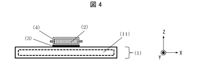
本発明のベイパーチャンバーの第4の実施形態として、図4に示されるように、被覆層が前記熱拡散部材の両面を被覆しており、面方向端部において、面方向へオフセット部が設けられていても良い。このようなオフセット部が設けられていることによって、熱拡散部材(2)の内部応力を抑えることができ、チャンバー本体(1)への配置が安定しやすい利点がある。オフセット部の幅としては、0.5mm以上あれば十分である。オフセット部を形成する方法としては、金属、またはセラミックスの板を接合する方法でオフセット部を形成する場合、絞り加工、切削加工、曲げ加工など公知の技術を用いて、熱拡散部材(2)を被覆でき、かつオフセット部を有する形状に金属、またはセラミックスの板を予め加工しておき、前述する本発明のベイパーチャンバーの第2の実施形態と同様に金属系ろう材で熱拡散部材(2)と接合したものを、チャンバー本体(1)に配置する方法が挙げられる。
本発明のベイパーチャンバーの第4の実施形態として、図4に示されるように、被覆層が前記熱拡散部材の両面を被覆しており、面方向端部において、面方向へオフセット部が設けられていても良い。このようなオフセット部が設けられていることによって、熱拡散部材(2)の内部応力を抑えることができ、チャンバー本体(1)への配置が安定しやすい利点がある。オフセット部の幅としては、0.5mm以上あれば十分である。オフセット部を形成する方法としては、金属、またはセラミックスの板を接合する方法でオフセット部を形成する場合、絞り加工、切削加工、曲げ加工など公知の技術を用いて、熱拡散部材(2)を被覆でき、かつオフセット部を有する形状に金属、またはセラミックスの板を予め加工しておき、前述する本発明のベイパーチャンバーの第2の実施形態と同様に金属系ろう材で熱拡散部材(2)と接合したものを、チャンバー本体(1)に配置する方法が挙げられる。
<半導体パッケージ>
本発明の一態様に係るベイパーチャンバーの前記熱拡散部材(2)と半導体素子(5)を接合して半導体パッケージとすることができる。更に、本発明の一態様に係るベイパーチャンバーの前記チャンバー本体(1)における前記半導体素子(5)を設置した側と反対側の面にヒートシンク(6)を有する半導体パッケージとすることができる。本発明の一態様に係るベイパーチャンバーを搭載する半導体パッケージは、半導体素子の温度上昇を効率的に抑制することを可能にする。図5に、本発明の第1の実施形態のベイパーチャンバーが搭載された半導体パッケージの第1の実施形態を示す。図6に、本発明の第3の実施形態のベイパーチャンバーが搭載された半導体パッケージの第2の実施形態の断面を示す。以下に、本発明の一態様に係るベイパーチャンバーを搭載する半導体パッケージを構成する各部材について説明する。
本発明の一態様に係るベイパーチャンバーの前記熱拡散部材(2)と半導体素子(5)を接合して半導体パッケージとすることができる。更に、本発明の一態様に係るベイパーチャンバーの前記チャンバー本体(1)における前記半導体素子(5)を設置した側と反対側の面にヒートシンク(6)を有する半導体パッケージとすることができる。本発明の一態様に係るベイパーチャンバーを搭載する半導体パッケージは、半導体素子の温度上昇を効率的に抑制することを可能にする。図5に、本発明の第1の実施形態のベイパーチャンバーが搭載された半導体パッケージの第1の実施形態を示す。図6に、本発明の第3の実施形態のベイパーチャンバーが搭載された半導体パッケージの第2の実施形態の断面を示す。以下に、本発明の一態様に係るベイパーチャンバーを搭載する半導体パッケージを構成する各部材について説明する。
<半導体素子(5)>
本発明一態様に係る半導体パッケージに用いられる半導体素子(5)は、特に限定されないが、CPU、GPU、FPGA、トランジスタ、ダイオード、メモリなどが挙げられる。
本発明一態様に係る半導体パッケージに用いられる半導体素子(5)は、特に限定されないが、CPU、GPU、FPGA、トランジスタ、ダイオード、メモリなどが挙げられる。
<ヒートシンク(6)>
本発明一態様に係る半導体パッケージに用いられるヒートシンク(6)は、特に限定されず、平行櫛型フィン、ピンフィン、コルゲートフィン、水冷式ヒートシンク、ペルチェモジュールなど公知のものを用いることができる。平行櫛型フィン、ピンフィン、コルゲートフィンの場合、冷却を促進するためにモーターファンを併用しても良い。
本発明一態様に係る半導体パッケージに用いられるヒートシンク(6)は、特に限定されず、平行櫛型フィン、ピンフィン、コルゲートフィン、水冷式ヒートシンク、ペルチェモジュールなど公知のものを用いることができる。平行櫛型フィン、ピンフィン、コルゲートフィンの場合、冷却を促進するためにモーターファンを併用しても良い。
<半導体パッケージの第1の実施形態>
本発明の第1の実施形態のベイパーチャンバーが搭載された半導体パッケージにおいて、蒸発部の有効面積を広げ、半導体素子の温度上昇を抑制する効果を効率的に得るための第1の実施形態としては、図5に示されるように、半導体素子(5)側から、半導体素子(5)、熱拡散部材(2)、チャンバー本体(1)、ヒートシンク(6)の順に構成されたものが挙げられる。熱拡散部材(2)と半導体素子(5)を接合する方法として、半田、熱伝導性グリース、熱伝導性シートなど公知のものを用いることが可能であるが、熱抵抗を極力低くする観点から、半田が好ましい。半田の種類としては特に制限されず、固体状、ペースト状のものを適宜用いることが出来る。また、チャンバー本体(1)とヒートシンク(6)を接合する方法として、半田、ろう材、拡散接合、熱伝導性グリース、熱伝導性シートなど公知のものを用いることが可能であるが、熱抵抗を極力低くする観点から、半田、ろう材、拡散接合が好ましく、取り扱いの観点から半田が特に好ましい。半田の種類としては特に制限されず、固体状、ペースト状のものを適宜用いることが出来る。
本発明の第1の実施形態のベイパーチャンバーが搭載された半導体パッケージにおいて、蒸発部の有効面積を広げ、半導体素子の温度上昇を抑制する効果を効率的に得るための第1の実施形態としては、図5に示されるように、半導体素子(5)側から、半導体素子(5)、熱拡散部材(2)、チャンバー本体(1)、ヒートシンク(6)の順に構成されたものが挙げられる。熱拡散部材(2)と半導体素子(5)を接合する方法として、半田、熱伝導性グリース、熱伝導性シートなど公知のものを用いることが可能であるが、熱抵抗を極力低くする観点から、半田が好ましい。半田の種類としては特に制限されず、固体状、ペースト状のものを適宜用いることが出来る。また、チャンバー本体(1)とヒートシンク(6)を接合する方法として、半田、ろう材、拡散接合、熱伝導性グリース、熱伝導性シートなど公知のものを用いることが可能であるが、熱抵抗を極力低くする観点から、半田、ろう材、拡散接合が好ましく、取り扱いの観点から半田が特に好ましい。半田の種類としては特に制限されず、固体状、ペースト状のものを適宜用いることが出来る。
<半導体パッケージの第2の実施形態>
本発明の第3の実施形態のベイパーチャンバーが搭載された半導体パッケージにおいて、蒸発部(7)の有効面積を広げ、半導体素子の温度上昇を抑制する効果を効率的に得るための第2の実施形態としては、図6に示されるように、半導体素子側から、半導体素子(5)、半導体素子(5)側に被覆層(4)が設けられた熱拡散部材(2)、チャンバー本体(1)、ヒートシンク(6)の順に構成されたものが挙げられる。被覆層(4)の形成方法としては、本発明のベイパーチャンバーの第2~4の実施形態と同様の方法を用いることが可能である。また、熱拡散部材(2)と半導体素子(5)を接合する方法、及び、チャンバー本体(1)とヒートシンク(6)を接合する方法としては、前述する半導体パッケージの第1の実施形態と同様の方法を用いることが可能である。本発明の第3の実施形態に係るベイパーチャンバーを搭載する半導体パッケージは、図6に示されるように、蒸発部(7)の面積が半導体素子(5)の面積よりも明らかに広くなり、かつ、凝縮部(8)の面積も十分広いため、半導体素子の温度上昇を効率的に抑制することを可能にする。
本発明の第3の実施形態のベイパーチャンバーが搭載された半導体パッケージにおいて、蒸発部(7)の有効面積を広げ、半導体素子の温度上昇を抑制する効果を効率的に得るための第2の実施形態としては、図6に示されるように、半導体素子側から、半導体素子(5)、半導体素子(5)側に被覆層(4)が設けられた熱拡散部材(2)、チャンバー本体(1)、ヒートシンク(6)の順に構成されたものが挙げられる。被覆層(4)の形成方法としては、本発明のベイパーチャンバーの第2~4の実施形態と同様の方法を用いることが可能である。また、熱拡散部材(2)と半導体素子(5)を接合する方法、及び、チャンバー本体(1)とヒートシンク(6)を接合する方法としては、前述する半導体パッケージの第1の実施形態と同様の方法を用いることが可能である。本発明の第3の実施形態に係るベイパーチャンバーを搭載する半導体パッケージは、図6に示されるように、蒸発部(7)の面積が半導体素子(5)の面積よりも明らかに広くなり、かつ、凝縮部(8)の面積も十分広いため、半導体素子の温度上昇を効率的に抑制することを可能にする。
以下に本発明の実施例について説明する。
(半導体素子の温度評価)
実施例1~9、比較例2~4は熱拡散部材のチャンバー本体側の面と反対側の面の中央部に、比較例1はチャンバー本体の第1外面中央部に熱伝導グリース(型番:G-775、信越化学工業株式会社製)を介して半導体素子(10mm×10mm)を接合し、チャンバー本体の第2外面には全面に、前記熱伝導グリースを介して水冷式ヒートシンク(水温25℃)を接合して半導体パッケージを製造した。半導体素子に100Wの熱を発生させ、熱電対を用いてその時の半導体素子の温度を測定した。半導体素子の温度が90℃未満であれば温度上昇の抑制効果は「A」、90℃以上100℃未満であれば「B」、100℃以上110℃未満であれば「C」、110℃以上であれば「D」とし、「A」もしくは「B」の時、ベイパーチャンバーの熱輸送量が高く、半導体パッケージにおける半導体素子の温度上昇を抑制出来ていると判断した。
(製造例1)
熱拡散部材に用いる異方性グラファイトAの原料となるグラファイトブロックは以下のように製造した。100mm×100mm×厚さ12.5μmの株式会社カネカ製のポリイミドフィルムを、20000枚積層した後、40kg/cm2の圧力でプレス加圧しながら、アルゴン雰囲気下、2200℃まで熱処理することによりグラファイトブロック(90mm×90mm、厚さ100mm)を作製した。得られたグラファイトブロックの結晶配向面に平行な方向の熱伝導率は600W/mK、結晶配向面に垂直な方向の熱伝導率は5W/mKであった。
熱拡散部材に用いる異方性グラファイトAの原料となるグラファイトブロックは以下のように製造した。100mm×100mm×厚さ12.5μmの株式会社カネカ製のポリイミドフィルムを、20000枚積層した後、40kg/cm2の圧力でプレス加圧しながら、アルゴン雰囲気下、2200℃まで熱処理することによりグラファイトブロック(90mm×90mm、厚さ100mm)を作製した。得られたグラファイトブロックの結晶配向面に平行な方向の熱伝導率は600W/mK、結晶配向面に垂直な方向の熱伝導率は5W/mKであった。
(製造例2)
熱拡散部材に用いる異方性グラファイトBの原料となるグラファイトブロックは以下のように製造した。100mm×100mm×厚さ12.5μmの株式会社カネカ製のポリイミドフィルムを、20000枚積層した後、40kg/cm2の圧力でプレス加圧しながら、アルゴン雰囲気下、2900℃まで熱処理することによりグラファイトブロック(90mm×90mm、厚さ100mm)を作製した。得られたグラファイトブロックの結晶配向面に平行な方向の熱伝導率は1500W/mK、結晶配向面に垂直な方向の熱伝導率は5W/mKであった。
熱拡散部材に用いる異方性グラファイトBの原料となるグラファイトブロックは以下のように製造した。100mm×100mm×厚さ12.5μmの株式会社カネカ製のポリイミドフィルムを、20000枚積層した後、40kg/cm2の圧力でプレス加圧しながら、アルゴン雰囲気下、2900℃まで熱処理することによりグラファイトブロック(90mm×90mm、厚さ100mm)を作製した。得られたグラファイトブロックの結晶配向面に平行な方向の熱伝導率は1500W/mK、結晶配向面に垂直な方向の熱伝導率は5W/mKであった。
(製造例3)
チャンバー本体は以下のように製造した。第1外面となる面を有する銅製の平板と、第2外面となる面を有する銅製の有底筒を用いて、サイズが100mm×100mm、厚みが5mmの方形中空筒状のものを準備した。内壁面の全面に多孔構造のウイックを配置し、液状物は純水とした。
チャンバー本体は以下のように製造した。第1外面となる面を有する銅製の平板と、第2外面となる面を有する銅製の有底筒を用いて、サイズが100mm×100mm、厚みが5mmの方形中空筒状のものを準備した。内壁面の全面に多孔構造のウイックを配置し、液状物は純水とした。
(実施例1)
製造例1で得たグラファイトブロックをワイヤーソー(型番:WSD-K2、株式会社タカトリ製)で切断して、平面のサイズが30mm×30mm、厚みが1.5mmの異方性グラファイトAを得た。前記異方性グラファイトAは結晶配向面が厚み方向に沿って配列しており、熱伝導率は600W/mKであった。この異方性グラファイトAを熱拡散部材として、製造例3で得たチャンバー本体の第1外面の中央部に熱伝導グリース(型番:G-775、信越化学工業株式会社製)を介して配置し、ベイパーチャンバーを製造した。
製造例1で得たグラファイトブロックをワイヤーソー(型番:WSD-K2、株式会社タカトリ製)で切断して、平面のサイズが30mm×30mm、厚みが1.5mmの異方性グラファイトAを得た。前記異方性グラファイトAは結晶配向面が厚み方向に沿って配列しており、熱伝導率は600W/mKであった。この異方性グラファイトAを熱拡散部材として、製造例3で得たチャンバー本体の第1外面の中央部に熱伝導グリース(型番:G-775、信越化学工業株式会社製)を介して配置し、ベイパーチャンバーを製造した。
前記ベイパーチャンバーを用いて、半導体素子の温度評価を行ったところ、半導体素子の温度は95℃であり、評価は「B」であった。
(実施例2)
製造例2で得たグラファイトブロックをワイヤーソー(型番:WSD-K2、株式会社タカトリ製)で切断し、熱拡散部材として、平面のサイズが30mm×30mm、厚みが1.5mmの異方性グラファイトBを得た。前記異方性グラファイトBは結晶配向面が厚み方向に沿って配列しており、熱伝導率は1500W/mKであった。前記熱拡散部材の平面側の片面全面にマスキングテープ(型番:851A、3M社製)を貼りつけた状態で電解めっきを行い、表面に0.01mm厚みのCuの被覆層を形成し、その後マスキングテープを除去して、片面のみにCuの被覆層が形成された熱拡散部材を製造した。製造例3で得たチャンバー本体の第1外面の中央部に熱伝導グリース(型番:G-775、信越化学工業株式会社製)を介して前記熱拡散部材のグラファイト露出面がチャンバー本体の第1外面に対向するよう配置し、図2に示されるようなベイパーチャンバーを製造した。
製造例2で得たグラファイトブロックをワイヤーソー(型番:WSD-K2、株式会社タカトリ製)で切断し、熱拡散部材として、平面のサイズが30mm×30mm、厚みが1.5mmの異方性グラファイトBを得た。前記異方性グラファイトBは結晶配向面が厚み方向に沿って配列しており、熱伝導率は1500W/mKであった。前記熱拡散部材の平面側の片面全面にマスキングテープ(型番:851A、3M社製)を貼りつけた状態で電解めっきを行い、表面に0.01mm厚みのCuの被覆層を形成し、その後マスキングテープを除去して、片面のみにCuの被覆層が形成された熱拡散部材を製造した。製造例3で得たチャンバー本体の第1外面の中央部に熱伝導グリース(型番:G-775、信越化学工業株式会社製)を介して前記熱拡散部材のグラファイト露出面がチャンバー本体の第1外面に対向するよう配置し、図2に示されるようなベイパーチャンバーを製造した。
前記ベイパーチャンバーを用いて、半導体素子の温度評価を行ったところ、半導体素子の温度は78℃であり、評価は「A」であった。
(実施例3)
厚み0.2mmの銅板上に、厚み0.013mmの活性銀ろう(型番:TKC-661、田中貴金属工業株式会社製)が予め形成されたクラッド材を準備し、金型を用いた絞り加工により、内寸が30mm×30mm×1.5mm、面方向端部のオフセット部の幅が1mmである、有底形状部品を製造した。前記有底形状部品に実施例2と同様にして得た熱拡散部材である異方性グラファイトBを装填した状態で、1×10⁻³Paの真空下で780℃、30分間加熱処理して両者を均一に接合し、片面のみに0.2mm厚みのCuの被覆層が形成された熱拡散部材を製造した。製造例3で得たチャンバー本体の第1外面の中央部に熱伝導グリース(型番:G-775、信越化学工業株式会社製)を介して前記熱拡散部材のグラファイト露出面がチャンバー本体の第1外面に対向するよう配置し、図3に示されるようなベイパーチャンバーを製造した。
厚み0.2mmの銅板上に、厚み0.013mmの活性銀ろう(型番:TKC-661、田中貴金属工業株式会社製)が予め形成されたクラッド材を準備し、金型を用いた絞り加工により、内寸が30mm×30mm×1.5mm、面方向端部のオフセット部の幅が1mmである、有底形状部品を製造した。前記有底形状部品に実施例2と同様にして得た熱拡散部材である異方性グラファイトBを装填した状態で、1×10⁻³Paの真空下で780℃、30分間加熱処理して両者を均一に接合し、片面のみに0.2mm厚みのCuの被覆層が形成された熱拡散部材を製造した。製造例3で得たチャンバー本体の第1外面の中央部に熱伝導グリース(型番:G-775、信越化学工業株式会社製)を介して前記熱拡散部材のグラファイト露出面がチャンバー本体の第1外面に対向するよう配置し、図3に示されるようなベイパーチャンバーを製造した。
前記ベイパーチャンバーを用いて、半導体素子の温度評価を行ったところ、半導体素子の温度は83℃であり、評価は「A」であった。
(実施例4)
異方性グラファイトBの厚みが3.0mm、銅板の厚みが0.3mm、有底形状部品の内寸が30mm×30mm×3.0mmであったこと以外は実施例3と同様にして、図3に示されるようなベイパーチャンバーを製造した。前記ベイパーチャンバーを用いて、半導体素子の温度評価を行ったところ、半導体素子の温度は82℃であり、評価は「A」であった。
異方性グラファイトBの厚みが3.0mm、銅板の厚みが0.3mm、有底形状部品の内寸が30mm×30mm×3.0mmであったこと以外は実施例3と同様にして、図3に示されるようなベイパーチャンバーを製造した。前記ベイパーチャンバーを用いて、半導体素子の温度評価を行ったところ、半導体素子の温度は82℃であり、評価は「A」であった。
(実施例5)
異方性グラファイトBの平面のサイズが98mm×98mm、厚みが5.0mm、有底形状部品の内寸が100mm×100mm×5.0mmであったこと以外は実施例3と同様にして、図3に示されるようなベイパーチャンバーを製造した。前記ベイパーチャンバーを用いて、半導体素子の温度評価を行ったところ、半導体素子の温度は88℃であり、評価は「A」であった。
異方性グラファイトBの平面のサイズが98mm×98mm、厚みが5.0mm、有底形状部品の内寸が100mm×100mm×5.0mmであったこと以外は実施例3と同様にして、図3に示されるようなベイパーチャンバーを製造した。前記ベイパーチャンバーを用いて、半導体素子の温度評価を行ったところ、半導体素子の温度は88℃であり、評価は「A」であった。
(実施例6)
窒化アルミニウムのブロックを内寸が30mm×30mm×1.5mm、オフセット部の幅が1mmになるように切削加工し、有底形状部品を製造した。前記有底形状部品に厚み0.013mmの活性銀ろう箔(型番:TKC-661、田中貴金属工業株式会社製)、実施例2と同様にして得た熱拡散部材である異方性グラファイトBを順に装填した状態で、1×10⁻³Paの真空下で780℃、30分間加熱処理して両者を均一に接合し、片面のみに0.2mm厚みの窒化アルミニウムの被覆層が形成された熱拡散部材を製造した。製造例3で得たチャンバー本体の第1外面の中央部に熱伝導グリース(型番:G-775、信越化学工業株式会社製)を介して前記熱拡散部材のグラファイト露出面がチャンバー本体の第1外面に対向するよう配置し、図3に示されるようなベイパーチャンバーを製造した。
窒化アルミニウムのブロックを内寸が30mm×30mm×1.5mm、オフセット部の幅が1mmになるように切削加工し、有底形状部品を製造した。前記有底形状部品に厚み0.013mmの活性銀ろう箔(型番:TKC-661、田中貴金属工業株式会社製)、実施例2と同様にして得た熱拡散部材である異方性グラファイトBを順に装填した状態で、1×10⁻³Paの真空下で780℃、30分間加熱処理して両者を均一に接合し、片面のみに0.2mm厚みの窒化アルミニウムの被覆層が形成された熱拡散部材を製造した。製造例3で得たチャンバー本体の第1外面の中央部に熱伝導グリース(型番:G-775、信越化学工業株式会社製)を介して前記熱拡散部材のグラファイト露出面がチャンバー本体の第1外面に対向するよう配置し、図3に示されるようなベイパーチャンバーを製造した。
前記ベイパーチャンバーを用いて、半導体素子の温度評価を行ったところ、半導体素子の温度は91℃であり、評価は「B」であった。
(実施例7)
異方性グラファイトBの平面のサイズが20mm×20mm、厚みが1.0mm、有底形状部品の内寸が20mm×20mm×1.0mmであったこと以外は実施例3と同様にして、図3に示されるようなベイパーチャンバーを製造した。前記ベイパーチャンバーを用いて、半導体素子の温度評価を行ったところ、半導体素子の温度は94℃であり、評価は「B」であった。
異方性グラファイトBの平面のサイズが20mm×20mm、厚みが1.0mm、有底形状部品の内寸が20mm×20mm×1.0mmであったこと以外は実施例3と同様にして、図3に示されるようなベイパーチャンバーを製造した。前記ベイパーチャンバーを用いて、半導体素子の温度評価を行ったところ、半導体素子の温度は94℃であり、評価は「B」であった。
(実施例8)
厚み0.2mmの銅板上に、厚み0.013mmの活性銀ろう(型番:TKC-661、田中貴金属工業株式会社製)が予め形成されたクラッド材を準備し、金型を用いた絞り加工により、内寸が70mm×70mm×1.5mm、オフセット部の幅が1mmである、有底形状部品を製造した。前記有底形状部品を2つ対向させて前記熱拡散部材である異方性グラファイトBを装填した状態で、1×10⁻³Paの真空下で780℃、30分間加熱処理して両者を均一に接合し、表面に0.2mm厚みのCuの被覆層が形成された熱拡散部材を製造した。製造例3で得たチャンバー本体の第1外面の中央部に熱伝導グリース(型番:G-775、信越化学工業株式会社製)を介して前記熱拡散部材の主面(70mm×70mmの面)がチャンバー本体の第1外面に対向するよう配置し、図4に示されるようなベイパーチャンバーを製造した。
厚み0.2mmの銅板上に、厚み0.013mmの活性銀ろう(型番:TKC-661、田中貴金属工業株式会社製)が予め形成されたクラッド材を準備し、金型を用いた絞り加工により、内寸が70mm×70mm×1.5mm、オフセット部の幅が1mmである、有底形状部品を製造した。前記有底形状部品を2つ対向させて前記熱拡散部材である異方性グラファイトBを装填した状態で、1×10⁻³Paの真空下で780℃、30分間加熱処理して両者を均一に接合し、表面に0.2mm厚みのCuの被覆層が形成された熱拡散部材を製造した。製造例3で得たチャンバー本体の第1外面の中央部に熱伝導グリース(型番:G-775、信越化学工業株式会社製)を介して前記熱拡散部材の主面(70mm×70mmの面)がチャンバー本体の第1外面に対向するよう配置し、図4に示されるようなベイパーチャンバーを製造した。
前記ベイパーチャンバーを用いて、半導体素子の温度評価を行ったところ、半導体素子の温度は82℃であり、評価は「A」であった。
(実施例9)
熱拡散部材として異方性グラファイトBを用いた以外は実施例1と同様にして、図1に示されるようなベイパーチャンバーを製造した。
熱拡散部材として異方性グラファイトBを用いた以外は実施例1と同様にして、図1に示されるようなベイパーチャンバーを製造した。
前記ベイパーチャンバーを用いて、半導体素子の温度評価を行ったところ、半導体素子の温度は77℃であり、評価は「A」であった。
(比較例1)
熱拡散部材を設置せずに、製造例3で得たチャンバー本体のみをベイパーチャンバーとして用いて、半導体素子の温度評価を行ったところ、半導体素子の温度は115℃であり、評価は「D」であった。
熱拡散部材を設置せずに、製造例3で得たチャンバー本体のみをベイパーチャンバーとして用いて、半導体素子の温度評価を行ったところ、半導体素子の温度は115℃であり、評価は「D」であった。
(比較例2)
熱拡散部材として純銅のものを用いた以外は実施例1と同様にして、図1に示されるようなベイパーチャンバーを製造した。
熱拡散部材として純銅のものを用いた以外は実施例1と同様にして、図1に示されるようなベイパーチャンバーを製造した。
前記ベイパーチャンバーを用いて、半導体素子の温度評価を行ったところ、半導体素子の温度は103℃であり、評価は「C」であった。
(比較例3)
平面のサイズが100mm×100mmである熱拡散部材を用いた以外は比較例2と同様にして、図1に示されるようなベイパーチャンバーを製造した。
平面のサイズが100mm×100mmである熱拡散部材を用いた以外は比較例2と同様にして、図1に示されるようなベイパーチャンバーを製造した。
前記ベイパーチャンバーを用いて、半導体素子の温度評価を行ったところ、半導体素子の温度は100℃であり、評価は「C」であった。
(比較例4)
厚みが5.0mmである熱拡散部材を用いた以外は比較例3と同様にして、図1に示されるようなベイパーチャンバーを製造した。
厚みが5.0mmである熱拡散部材を用いた以外は比較例3と同様にして、図1に示されるようなベイパーチャンバーを製造した。
前記ベイパーチャンバーを用いて、半導体素子の温度評価を行ったところ、半導体素子の温度は110℃であり、評価は「D」であった。
以下の表1に、実施例および比較例の構成と評価結果をまとめた。表1から、500W/mK以上の熱伝導率を有する熱拡散部材が配置されたベイパーチャンバーが半導体素子の温度上昇の抑制に効果があることは明らかである。

本発明の一態様に係るベイパーチャンバーは、以下に関する。
(I)内部に密封空間を有するチャンバー本体と、
前記チャンバー本体に封入された液状物と、
熱拡散部材とを有するベイパーチャンバーであって、
前記チャンバー本体は第1外面と、前記第1外面の裏面である第1内面と、第2外面と、前記第2外面の裏面である第2内面とを有し、
前記第1内面と前記第2内面との間に前記密封空間を有しており、
前記液状物は前記密封空間内に封入されており、前記チャンバー本体の前記第1外面および/または前記第2外面に前記熱拡散部材を備えており、
前記熱拡散部材は、前記チャンバー本体の前記第1外面または前記第2外面に対して直交する面方向の熱伝導率が500W/mK以上であるベイパーチャンバー。
(II)前記熱拡散部材が異方性グラファイトを含む、(I)に記載のベイパーチャンバー。
(III)前記異方性グラファイトの結晶配向面は、前記第1外面または前記第2外面に対して直交する面に対し±10度以内の角度をなす、(II)に記載のベイパーチャンバー。
(IV)前記チャンバー本体が金属である、(I)~(III)のいずれかに記載のベイパーチャンバー。
(V)前記熱拡散部材と前記チャンバー本体が接合層を介して接合されており、前記接合層は半田、ろう材、拡散接合、及び熱伝導性グリースよりなる群から選ばれる少なくとも1種を含む、(I)~(IV)のいずれかに記載のベイパーチャンバー。
(VI)前記熱拡散部材の表面の少なくとも一部に金属、またはセラミックスのいずれかを含む被覆層をさらに有する、(I)~(V)のいずれかに記載のベイパーチャンバー。
(VII)前記被覆層の厚みが0.005~0.5mmである、(VI)に記載のベイパーチャンバー。
(VIII)前記被覆層が前記熱拡散部材の面方向端部において、面方向への幅が0.5mm以上のオフセット領域が設けられている、(VI)または(VII)に記載のベイパーチャンバー。
(IX)前記熱拡散部材の厚みが0.5~10.0mmである(I)~(VIII)のいずれかに記載のベイパーチャンバー。
(X)前記熱拡散部材の面方向の面積が前記チャンバー本体の前記第1外面または前記第2外面の面積の4~100%である(I)~(IX)のいずれかに記載のベイパーチャンバー。
(XI)半導体素子と、(I)~(X)のいずれかに記載のベイパーチャンバーとを有し、前記熱拡散部材と前記半導体素子が接合されている半導体パッケージ。
(XII)前記チャンバー本体の前記熱拡散部材側の面と反対側の面にヒートシンクを有する、(XI)に記載の半導体パッケージ。
本発明の一態様に係るベイパーチャンバーは、半導体素子の温度上昇を抑制可能な半導体パッケージを提供することに好適である。
(1) チャンバー本体
(11) 液状物
(2) 熱拡散部材
(3) 接合層
(4) 被覆層
(5) 半導体素子
(6) ヒートシンク
(7) 蒸発部
(8) 凝縮部
(11) 液状物
(2) 熱拡散部材
(3) 接合層
(4) 被覆層
(5) 半導体素子
(6) ヒートシンク
(7) 蒸発部
(8) 凝縮部
Claims (12)
- 内部に密封空間を有するチャンバー本体と、
前記チャンバー本体に封入された液状物と、
熱拡散部材とを有するベイパーチャンバーであって、
前記チャンバー本体は第1外面と、前記第1外面の裏面である第1内面と、第2外面と、前記第2外面の裏面である第2内面とを有し、
前記第1内面と前記第2内面との間に前記密封空間を有しており、
前記液状物は前記密封空間内に封入されており、
前記チャンバー本体の前記第1外面および/または前記第2外面に前記熱拡散部材を備えており、
前記熱拡散部材は、前記チャンバー本体の前記第1外面または前記第2外面に対して直交する面方向の熱伝導率が500W/mK以上であるベイパーチャンバー。 - 前記熱拡散部材が異方性グラファイトを含む、請求項1に記載のベイパーチャンバー。
- 前記異方性グラファイトの結晶配向面は、前記第1外面または前記第2外面に対して直交する面に対し±10度以内の角度をなす、請求項2に記載のベイパーチャンバー。
- 前記チャンバー本体が金属である、請求項1~3のいずれか1項に記載のベイパーチャンバー。
- 前記熱拡散部材と前記チャンバー本体が接合層を介して接合されており、前記接合層は半田、ろう材、拡散接合、及び熱伝導性グリースよりなる群から選ばれる少なくとも1種を含む、請求項1~4のいずれか1項に記載のベイパーチャンバー。
- 前記熱拡散部材の表面の少なくとも一部に金属、またはセラミックスのいずれかを含む被覆層をさらに有する、請求項1~5のいずれか1項に記載のベイパーチャンバー。
- 前記被覆層の厚みが0.005~0.5mmである、請求項6に記載のベイパーチャンバー。
- 前記被覆層が前記熱拡散部材の面方向端部において、面方向への幅が0.5mm以上のオフセット領域が設けられている、請求項6または7に記載のベイパーチャンバー。
- 前記熱拡散部材の厚みが0.5~10.0mmである請求項1~8のいずれか1項に記載のベイパーチャンバー。
- 前記熱拡散部材の面方向の面積が前記チャンバー本体の前記第1外面または前記第2外面の面積の4~100%である請求項1~9のいずれか1項に記載のベイパーチャンバー。
- 半導体素子と、請求項1~10のいずれか1項に記載のベイパーチャンバーとを有し、前記熱拡散部材と前記半導体素子が接合されている半導体パッケージ。
- 前記チャンバー本体の前記熱拡散部材側の面と反対側の面にヒートシンクを有する、請求項11に記載の半導体パッケージ。
Priority Applications (3)
| Application Number | Priority Date | Filing Date | Title |
|---|---|---|---|
| CN202180053897.2A CN116018678A (zh) | 2020-09-02 | 2021-09-02 | 导热板、以及安装有此导热板的半导体封装体 |
| JP2022546960A JPWO2022050337A1 (ja) | 2020-09-02 | 2021-09-02 | |
| US18/176,210 US20230207425A1 (en) | 2020-09-02 | 2023-02-28 | Vapor chamber and semiconductor package having same mounted thereon |
Applications Claiming Priority (2)
| Application Number | Priority Date | Filing Date | Title |
|---|---|---|---|
| JP2020-147802 | 2020-09-02 | ||
| JP2020147802 | 2020-09-02 |
Related Child Applications (1)
| Application Number | Title | Priority Date | Filing Date |
|---|---|---|---|
| US18/176,210 Continuation US20230207425A1 (en) | 2020-09-02 | 2023-02-28 | Vapor chamber and semiconductor package having same mounted thereon |
Publications (1)
| Publication Number | Publication Date |
|---|---|
| WO2022050337A1 true WO2022050337A1 (ja) | 2022-03-10 |
Family
ID=80491082
Family Applications (1)
| Application Number | Title | Priority Date | Filing Date |
|---|---|---|---|
| PCT/JP2021/032236 WO2022050337A1 (ja) | 2020-09-02 | 2021-09-02 | ベイパーチャンバー、及び、これを搭載する半導体パッケージ |
Country Status (4)
| Country | Link |
|---|---|
| US (1) | US20230207425A1 (ja) |
| JP (1) | JPWO2022050337A1 (ja) |
| CN (1) | CN116018678A (ja) |
| WO (1) | WO2022050337A1 (ja) |
Citations (8)
| Publication number | Priority date | Publication date | Assignee | Title |
|---|---|---|---|---|
| JP2003124665A (ja) * | 2001-10-11 | 2003-04-25 | Fujikura Ltd | 電子装置用放熱構造 |
| JP2008522129A (ja) * | 2004-12-01 | 2008-06-26 | コンバージェンス テクノロジーズ リミテッド | 沸騰促進マルチウィック構造物を備えた蒸気チャンバー |
| JP2015050323A (ja) * | 2013-09-02 | 2015-03-16 | 株式会社フジクラ | 半導体パッケージの複合冷却構造 |
| WO2016098890A1 (ja) * | 2014-12-18 | 2016-06-23 | 株式会社カネカ | グラファイト積層体、グラファイト積層体の製造方法、熱輸送用構造物およびロッド状の熱輸送体 |
| JP2017216350A (ja) * | 2016-05-31 | 2017-12-07 | 日産自動車株式会社 | 半導体装置 |
| WO2019102665A1 (ja) * | 2017-11-21 | 2019-05-31 | ローム株式会社 | 半導体装置、パワーモジュールおよび電源装置 |
| JP2019140332A (ja) * | 2018-02-14 | 2019-08-22 | トヨタ自動車株式会社 | 半導体装置 |
| WO2019188614A1 (ja) * | 2018-03-28 | 2019-10-03 | 株式会社カネカ | 半導体パッケージ |
-
2021
- 2021-09-02 JP JP2022546960A patent/JPWO2022050337A1/ja active Pending
- 2021-09-02 WO PCT/JP2021/032236 patent/WO2022050337A1/ja active Application Filing
- 2021-09-02 CN CN202180053897.2A patent/CN116018678A/zh active Pending
-
2023
- 2023-02-28 US US18/176,210 patent/US20230207425A1/en active Pending
Patent Citations (8)
| Publication number | Priority date | Publication date | Assignee | Title |
|---|---|---|---|---|
| JP2003124665A (ja) * | 2001-10-11 | 2003-04-25 | Fujikura Ltd | 電子装置用放熱構造 |
| JP2008522129A (ja) * | 2004-12-01 | 2008-06-26 | コンバージェンス テクノロジーズ リミテッド | 沸騰促進マルチウィック構造物を備えた蒸気チャンバー |
| JP2015050323A (ja) * | 2013-09-02 | 2015-03-16 | 株式会社フジクラ | 半導体パッケージの複合冷却構造 |
| WO2016098890A1 (ja) * | 2014-12-18 | 2016-06-23 | 株式会社カネカ | グラファイト積層体、グラファイト積層体の製造方法、熱輸送用構造物およびロッド状の熱輸送体 |
| JP2017216350A (ja) * | 2016-05-31 | 2017-12-07 | 日産自動車株式会社 | 半導体装置 |
| WO2019102665A1 (ja) * | 2017-11-21 | 2019-05-31 | ローム株式会社 | 半導体装置、パワーモジュールおよび電源装置 |
| JP2019140332A (ja) * | 2018-02-14 | 2019-08-22 | トヨタ自動車株式会社 | 半導体装置 |
| WO2019188614A1 (ja) * | 2018-03-28 | 2019-10-03 | 株式会社カネカ | 半導体パッケージ |
Also Published As
| Publication number | Publication date |
|---|---|
| JPWO2022050337A1 (ja) | 2022-03-10 |
| US20230207425A1 (en) | 2023-06-29 |
| CN116018678A (zh) | 2023-04-25 |
Similar Documents
| Publication | Publication Date | Title |
|---|---|---|
| EP0435473B1 (en) | Evaporator having etched fiber nucleation sites and method of fabricating same | |
| JP5577980B2 (ja) | ヒートシンク付パワーモジュール用基板、パワーモジュール及びヒートシンク付パワーモジュール用基板の製造方法 | |
| JP2016026391A (ja) | 異方性熱伝導要素およびその製造方法 | |
| JPH0364097A (ja) | ヒート・シンク基板 | |
| CN110192273B (zh) | 用于在热接地平面中散布高热通量的方法和设备 | |
| JP2014515876A (ja) | 高熱伝導率/低熱膨張率を有する複合材 | |
| JP2010147478A (ja) | マイクロチャネルヒートシンクの低コスト製造 | |
| US20200413566A1 (en) | Heat conducting structure, manufacturing method thereof, and mobile device | |
| CN111725144A (zh) | 基于气液相变的高温电子封装基板材料器件及其制备方法 | |
| US20120268895A1 (en) | Electronic power module, and method for manufacturing said module | |
| US20070295482A1 (en) | Heat spreader for use in conjunction with a semiconducting device and method of manufacturing same | |
| WO2022050337A1 (ja) | ベイパーチャンバー、及び、これを搭載する半導体パッケージ | |
| CN114446903A (zh) | 封装器件、封装模组和电子设备 | |
| WO2003017365A2 (en) | Thermal transfer devices using heat pipes | |
| JP2005077052A (ja) | 平面型ヒートパイプ | |
| JP2021100006A (ja) | 半導体パッケージ | |
| JP7248280B2 (ja) | 熱伝導構造体、熱拡散装置 | |
| JP6040570B2 (ja) | 熱交換器 | |
| JP2004160549A (ja) | セラミックス−金属複合体およびこれを用いた高熱伝導放熱用基板 | |
| CN110944493B (zh) | 一种基于气液相变的金属基复合材料器件及其制备方法 | |
| KR20220165595A (ko) | 복합재료 및 방열부품 | |
| CN112781418A (zh) | 热传导部件 | |
| WO2019106874A1 (ja) | 絶縁基板及び放熱装置 | |
| JP2020191347A (ja) | 冷却装置 | |
| JP6708498B2 (ja) | 冷却器及びその製造方法 |
Legal Events
| Date | Code | Title | Description |
|---|---|---|---|
| 121 | Ep: the epo has been informed by wipo that ep was designated in this application |
Ref document number: 21864392 Country of ref document: EP Kind code of ref document: A1 |
|
| ENP | Entry into the national phase |
Ref document number: 2022546960 Country of ref document: JP Kind code of ref document: A |
|
| NENP | Non-entry into the national phase |
Ref country code: DE |
|
| 122 | Ep: pct application non-entry in european phase |
Ref document number: 21864392 Country of ref document: EP Kind code of ref document: A1 |