WO2022050260A1 - 弾性波装置 - Google Patents
弾性波装置 Download PDFInfo
- Publication number
- WO2022050260A1 WO2022050260A1 PCT/JP2021/031896 JP2021031896W WO2022050260A1 WO 2022050260 A1 WO2022050260 A1 WO 2022050260A1 JP 2021031896 W JP2021031896 W JP 2021031896W WO 2022050260 A1 WO2022050260 A1 WO 2022050260A1
- Authority
- WO
- WIPO (PCT)
- Prior art keywords
- density
- piezoelectric film
- region
- elastic wave
- film
- Prior art date
- Legal status (The legal status is an assumption and is not a legal conclusion. Google has not performed a legal analysis and makes no representation as to the accuracy of the status listed.)
- Ceased
Links
Images


Classifications
-
- H—ELECTRICITY
- H03—ELECTRONIC CIRCUITRY
- H03H—IMPEDANCE NETWORKS, e.g. RESONANT CIRCUITS; RESONATORS
- H03H9/00—Networks comprising electromechanical or electro-acoustic elements; Electromechanical resonators
- H03H9/02—Details
- H03H9/02535—Details of surface acoustic wave devices
- H03H9/02543—Characteristics of substrate, e.g. cutting angles
- H03H9/02559—Characteristics of substrate, e.g. cutting angles of lithium niobate or lithium-tantalate substrates
-
- H—ELECTRICITY
- H03—ELECTRONIC CIRCUITRY
- H03H—IMPEDANCE NETWORKS, e.g. RESONANT CIRCUITS; RESONATORS
- H03H9/00—Networks comprising electromechanical or electro-acoustic elements; Electromechanical resonators
- H03H9/02—Details
- H03H9/125—Driving means, e.g. electrodes, coils
- H03H9/13—Driving means, e.g. electrodes, coils for networks consisting of piezoelectric or electrostrictive materials
-
- H—ELECTRICITY
- H03—ELECTRONIC CIRCUITRY
- H03H—IMPEDANCE NETWORKS, e.g. RESONANT CIRCUITS; RESONATORS
- H03H9/00—Networks comprising electromechanical or electro-acoustic elements; Electromechanical resonators
- H03H9/02—Details
- H03H9/02535—Details of surface acoustic wave devices
- H03H9/02543—Characteristics of substrate, e.g. cutting angles
- H03H9/02574—Characteristics of substrate, e.g. cutting angles of combined substrates, multilayered substrates, piezoelectrical layers on not-piezoelectrical substrate
-
- H—ELECTRICITY
- H03—ELECTRONIC CIRCUITRY
- H03H—IMPEDANCE NETWORKS, e.g. RESONANT CIRCUITS; RESONATORS
- H03H9/00—Networks comprising electromechanical or electro-acoustic elements; Electromechanical resonators
- H03H9/02—Details
- H03H9/125—Driving means, e.g. electrodes, coils
- H03H9/145—Driving means, e.g. electrodes, coils for networks using surface acoustic waves
- H03H9/14538—Formation
-
- H—ELECTRICITY
- H03—ELECTRONIC CIRCUITRY
- H03H—IMPEDANCE NETWORKS, e.g. RESONANT CIRCUITS; RESONATORS
- H03H9/00—Networks comprising electromechanical or electro-acoustic elements; Electromechanical resonators
- H03H9/15—Constructional features of resonators consisting of piezoelectric or electrostrictive material
- H03H9/17—Constructional features of resonators consisting of piezoelectric or electrostrictive material having a single resonator
- H03H9/176—Constructional features of resonators consisting of piezoelectric or electrostrictive material having a single resonator consisting of ceramic material
-
- H—ELECTRICITY
- H03—ELECTRONIC CIRCUITRY
- H03H—IMPEDANCE NETWORKS, e.g. RESONANT CIRCUITS; RESONATORS
- H03H9/00—Networks comprising electromechanical or electro-acoustic elements; Electromechanical resonators
- H03H9/25—Constructional features of resonators using surface acoustic waves
Definitions
- the present invention relates to an elastic wave device used in an elastic wave resonator and an elastic wave filter.
- Patent Document 1 discloses an elastic wave device having a piezoelectric film made of LiTaO 3 .
- a low sound velocity film and a piezoelectric film are laminated on a high sound velocity support substrate.
- An IDT electrode is provided on the piezoelectric film.
- the film thickness of the piezoelectric film is in the range of 0.05 ⁇ to 0.5 ⁇ , where ⁇ is the wavelength determined by the electrode period of the ITD electrode. By doing so, it is said that the Q value can be increased.
- An object of the present invention is to provide an elastic wave device capable of suppressing out-of-band spurious.
- the first invention of the present application comprises a support substrate, a piezoelectric film provided on the support substrate, and an IDT electrode provided on the piezoelectric film, and the film thickness of the piezoelectric film is the IDT electrode.
- the wavelength of the elastic wave determined by the period of the electrode finger is ⁇ , it is set to 1 ⁇ or less, and the piezoelectric film has a first region and a second region in the thickness direction of the piezoelectric film.
- the density in the first region is the first density and the density in the second region is the second density, the first density and the second density are different. It is a wave device.
- the second invention of the present application includes a support substrate, a piezoelectric film provided on the support substrate, and an IDT electrode provided on the piezoelectric film, and the film thickness of the piezoelectric film is the IDT electrode.
- the wavelength of the elastic wave determined by the period of the electrode finger is ⁇ , it is set to 1 ⁇ or less, and the piezoelectric film is directly or indirectly laminated with the first piezoelectric film and the first piezoelectric film.
- the first piezoelectric film and the second piezoelectric film are made of a piezoelectric material of the same system, and the density of the first piezoelectric film is defined as the first density.
- the density of the second piezoelectric film is the second density, it is an elastic wave device in which the first density and the second density are different.
- the present invention it is possible to provide an elastic wave device capable of suppressing out-of-band spurious.
- FIG. 1 (a) and 1 (b) are a front sectional view and a schematic plan view showing an electrode structure of the elastic wave device according to the first embodiment of the present invention.
- FIG. 2 is a plan view for explaining the electrode finger pitch P of the IDT electrode and the wavelength ⁇ in the elastic wave device according to the first embodiment.
- FIG. 3 is a front sectional view for explaining the structure of the piezoelectric film of the elastic wave device according to the first embodiment.
- FIG. 4 is a diagram showing the phase-frequency characteristics of Example 1 and Comparative Example 1.
- FIG. 5 is a diagram showing the phase-frequency characteristics of Example 2 and Comparative Example 1.
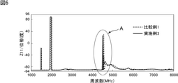
- FIG. 6 is a diagram showing the phase-frequency characteristics of Example 3 and Comparative Example 1.
- FIG. 7 is a diagram showing a phase-frequency characteristic in which the portion indicated by the ellipse A in FIG. 6 is enlarged.
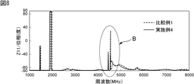
- FIG. 8 is a diagram showing the phase-frequency characteristics of Example 4 and Comparative Example 1.
- FIG. 9 is a diagram showing a phase-frequency characteristic in which the portion indicated by the ellipse B in FIG. 8 is enlarged.
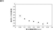
- FIG. 10 is a diagram showing the relationship between the thickness of the first region and the phase of the higher-order mode.
- FIG. 11 is a front sectional view of the piezoelectric film in the elastic wave device according to the second embodiment.
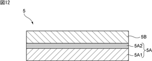
- FIG. 12 is a front sectional view of the piezoelectric film in the elastic wave device according to the third embodiment.
- FIG. 13 is a front sectional view for explaining a modified example of the elastic wave device of the present invention.
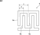
- FIG. 1A is a front sectional view of the elastic wave device according to the first embodiment of the present invention
- FIG. 1B is a schematic plan view showing the electrode structure thereof.
- the elastic wave device 1 has a support substrate 2.
- the high sound velocity material layer 3, the low sound velocity material layer 4, and the piezoelectric film 5 are laminated in this order on the support substrate 2. That is, the piezoelectric film 5 is indirectly provided on the support substrate 2.
- An IDT electrode 6 and reflectors 7 and 8 are provided on the piezoelectric film 5.
- a protective film made of silicon oxide or the like may be provided so as to cover the piezoelectric film 5, the IDT electrode 6, and the reflectors 7 and 8.
- an elastic surface wave device which is a 1-port type surface acoustic wave resonator, is configured.
- a plurality of first electrode fingers 6a and a plurality of second electrode fingers 6b are interleaved with each other.
- the distance between the centers of the first electrode finger 6a and the second electrode finger 6b is the electrode finger pitch P.
- the support substrate 2 is made of an appropriate insulating material such as silicon, alumina, or crystal, or a semiconductor material.
- the high sound velocity material layer 3 is made of a high sound velocity material in which the sound velocity of the propagating bulk wave is higher than the sound velocity of the elastic wave propagating in the piezoelectric film 5.
- the high-pitched sound speed material is not particularly limited, but is silicon, aluminum nitride, aluminum oxide, silicon nitride, silicon carbide, sapphire, lithium tantalate, lithium niobate, crystal, alumina, zirconia, cozilite, mulite, steatite, etc. Examples thereof include forsterite, magnesia, DLC (diamond-like carbon) film or diamond, and materials containing the above materials as main components. Further, at least one selected from the group consisting of aluminum nitride, aluminum oxide, silicon nitride and DLC is preferably used.
- the low sound velocity material layer 4 is made of a low sound velocity material in which the sound velocity of the propagating bulk wave is lower than the sound velocity of the bulk wave propagating through the piezoelectric film 5.
- the low sound velocity material is not particularly limited, and examples thereof include silicon oxide, silicon nitride, tantalum oxide or glass, and a compound obtained by adding fluorine, carbon, or boron to silicon oxide. Further, the low sound velocity material may be a material containing each of the above materials as a main component.
- the hypersonic material layer 3 is made of silicon nitride
- the low sound velocity material layer 4 is made of silicon oxide.
- the piezoelectric film 5 is made of LiTaO 3 .
- the piezoelectric film 5 may be made of a piezoelectric material other than lithium tantalate, for example, lithium niobate.
- the IDT electrode 6 and the reflectors 7 and 8 are made of an appropriate metal or alloy.
- the IDT electrode 6 and the reflectors 7 and 8 may be composed of a laminated body of a plurality of metal films.
- a feature of the elastic wave device 1 is that, as shown in FIGS. 1A and 3, the piezoelectric film 5 has a first region 5a and a second region 5b in the thickness direction. The second region 5b is located on the IDT electrode 6 side.
- the densities of the first region 5a and the second region 5b are different. That is, when the density of the first region 5a is the first density and the density of the second region 5b is the second density, the first density and the second density are different.
- the first region 5a and the second region 5b having different densities can be formed by adjusting the density of the ion-implanted region by, for example, ion-implanting hydrogen ions or the like into the piezoelectric film 5.
- the second region 5b may be formed after the first region 5a is formed.
- the first density and the second density can be made different. In this embodiment, the first density is higher than the second density.
- the densities of the first and second regions 5a and 5b of the piezoelectric film 5 can be obtained from the interstitial map obtained by using X-rays by changing the distance between the lattices, or the cross section of the piezoelectric film 5. It can be obtained by determining the proportion of a portion having a light color, that is, a portion having a low density, and comparing it with a photograph of a single crystal.
- the elastic wave device 1 Since the elastic wave device 1 has the first and second regions 5a and 5b having different densities, it is possible to reduce out-of-band spurious. It is considered that this is because the second region 5b, which has a relatively low density, changes the higher-order mode to the leakage mode and reduces out-of-band spurious.
- one of the first region 5a and the second region 5b has, for example, the theoretical density of the piezoelectric single crystal.
- the theoretical density is 7.454 ⁇ 10 3 (kg / m 3 ).
- the second region 5b where the IDT electrode 6 is provided has this theoretical density. In that case, good piezoelectric characteristics can be obtained.
- the density of the first region 5a and the density of the second region 5b may both be higher or lower than the theoretical density.
- Example 1 was configured with the following design parameters.
- the film thickness of the first region 5a 200 nm
- the film thickness of the second region 5b 200 nm
- the density of the first region 5a 7.454 ⁇ 10 3 (kg / m 3 ), and this value is equal to the theoretical density of LiTaO 3 .
- the density of the second region 5b 0.8 times the density of the first region 5a. Therefore, the first density> the second density.
- IDT electrode 6 and reflectors 7, 8 A laminate of a Ti film having a thickness of 12 nm, an AlCu film having a thickness of 100 nm, and a Ti film having a thickness of 4 nm from the piezoelectric film 5 side.
- a protective film a silicon oxide film having a thickness of 35 nm was provided so as to cover the IDT electrode 6 and the reflectors 7 and 8.
- the wavelength ⁇ 2 ⁇ m determined by the electrode finger pitch P of the IDT electrode 6 and the duty were 0.5.
- the elastic wave apparatus of Comparative Example 1 was configured in the same manner as in Example 1 except that a LiTaO 3 film having a thickness of 400 nm and a density of 7.454 ⁇ 10 3 (kg / m 3 ) was used. did.
- FIG. 4 shows the phase-frequency characteristics of the elastic wave devices of Example 1 and Comparative Example 1.
- the solid line shows the result of Example 1, and the broken line shows the result of Comparative Example 1.
- Example 1 In the elastic wave devices of Example 1 and Comparative Example 1, the band between the resonance frequency and the antiresonance frequency exists in the vicinity of 2000 MHz. Then, in Comparative Example 1, the out-of-band spurious that seems to be caused by the higher-order mode appears largely at around 4600 MHz. On the other hand, in Example 1, it can be seen that this large spurious is suppressed. It is considered that this is because the piezoelectric film 5 has the first and second regions 5a and 5b having different densities, so that the higher-order mode is escaped as the leakage mode.
- the film thickness of the first region 5a 200 nm
- the film thickness of the second region 5b 200 nm
- the density of the first region 5a 0.8 times the density of the second region 5b.
- IDT electrode 6 and reflectors 7, 8 A laminate of a Ti film having a thickness of 12 nm, an AlCu film having a thickness of 100 nm, and a Ti film having a thickness of 4 nm from the piezoelectric film 5 side.
- a protective film a silicon oxide film having a thickness of 35 nm was provided so as to cover the IDT electrode 6 and the reflectors 7 and 8.
- the wavelength ⁇ 2 ⁇ m determined by the electrode finger pitch P of the IDT electrode 6 and the duty were 0.5.
- Example 2 the density of the second region 5b was 7.454 ⁇ 10 3 (kg / m 3 ), and the density of the first region 5a was 0.8 times the density of the second region 5b. .. Therefore, the first density ⁇ the second density.
- Other configurations were the same as in Example 1 in Example 2.
- FIG. 5 shows the phase-frequency characteristics of Example 2 and Comparative Example 1.
- the broken line shows the result of Comparative Example 1, and the solid line shows the result of Example 2.
- Example 2 it is possible to effectively suppress spurious emissions that are considered to be due to the higher-order mode near 4600 MHz.
- Example 3 In the piezoelectric film 5, the second density of the second region 5b was set to 1.1 times the first density of the first region 5a. Other configurations were the same as in Example 1, and the elastic wave device of Example 3 was configured. Therefore, in Example 3, the first density ⁇ the second density.
- FIG. 6 is a diagram showing the phase-frequency characteristics of Example 3 and Comparative Example 1. Further, FIG. 7 is a phase-frequency characteristic diagram showing an enlarged portion indicated by the ellipse A in FIG. The broken line shows the result of Comparative Example 1, and the solid line shows the result of Example 3.
- Example 4 The density of the second region 5b was 7.454 ⁇ 10 3 (kg / m 3 ), and the density of the first region 5a was 1.1 times the density of the second region 5b. That is, the first density> the second density.
- FIG. 8 shows the phase-frequency characteristics of Example 4 and Comparative Example 1
- FIG. 9 is a phase-frequency characteristic diagram showing an enlarged portion of the part shown by the ellipse B in FIG.
- the piezoelectric film 5 has a first region 5a and a second region 5b having different densities, so that the order is higher. Out-of-band spurious that seems to be due to the mode can be suppressed.
- FIG. 10 is a diagram showing the relationship between the thickness of the first region 5a and the phase of the higher-order mode in the obtained elastic wave device in the above-mentioned Example 5.
- the thickness of the first region 5a increases, the spurious in the higher-order mode becomes smaller.
- the thickness of the first region 5a is 0.2 ⁇ m or more, that is, 0.1 ⁇ or more, in which case the higher-order mode can be suppressed more effectively.
- FIG. 11 is a front sectional view showing the piezoelectric film 5 in the elastic wave device according to the second embodiment.
- the piezoelectric film 5 has a first piezoelectric film 5A and a second piezoelectric film 5B.
- the piezoelectric film 5 is not limited to the one having the first and second regions 5a and 5b having different densities, and the first piezoelectric film 5A and the second piezoelectric film 5B are laminated. It may have a structure. Also in this case, the density of the first piezoelectric film 5A is the first density, and the density of the second piezoelectric film 5B is the second density.
- the second piezoelectric film 5B is located on the IDT electrode side.
- the first piezoelectric film 5A and the second piezoelectric film 5B are both made of the same piezoelectric material.
- the piezoelectric material of the same system for example, a combination of a piezoelectric single crystal and a material obtained by adding or doping the piezoelectric single crystal with impurities can be considered. More specifically, to give a more specific example, there is an example in which the first piezoelectric film 5A is formed of a material obtained by doping lithium tantalate with impurities, and lithium tantalate is used as the second piezoelectric film 5B.
- FIG. 12 is a front sectional view for explaining the piezoelectric film 5 in the elastic wave device according to the third embodiment.
- the piezoelectric film 5 has a first piezoelectric film 5A and a second piezoelectric film 5B.
- the first piezoelectric film 5A has a first portion 5A1 and a second portion 5A2 laminated on the first portion 5A1.
- the first portion 5A1 is a low density region having a relatively low density
- the second portion 5A2 is a high density region having a relatively higher density than the first portion 5A1.
- the second portion 5A2 which is a high-density region and the first portion 5A1 which is a low-density region are arranged along the thickness direction of the first piezoelectric film 5A.
- the first piezoelectric film 5A may have a plurality of regions having different densities. Such a structure can be obtained, for example, by forming the first portion 5A1 and then implanting ions from one surface to provide the second portion 5A2.
- the method for forming the first and second portions 5A1 and 5A2 having different densities is not particularly limited.
- the first piezoelectric film 5A has portions 5A1 and 5A2 having different densities, but the second piezoelectric film 5B side may be provided so as to have a plurality of portions having different densities. .. Further, both the first piezoelectric film 5A and the second piezoelectric film 5B may be provided with a plurality of portions having different densities. Further, the number of portions having different densities may be 3 or more.
- the piezoelectric film 5 is not limited to the laminate of the first piezoelectric film and the second piezoelectric film, and the third piezoelectric film is laminated in addition to the first piezoelectric film and the second piezoelectric film. It may have a structure.
- the high sound velocity material layer 3 and the low sound velocity material layer 4 are laminated between the support substrate 2 and the piezoelectric film 5, but as in the modified example shown in FIG. 13, the high sound velocity support substrate 2A and the high sound velocity support substrate 2A are laminated.
- the structure may be such that the low sound velocity material layer 4 is laminated with the piezoelectric film 5.
- the hypersonic support substrate 2A is made of the above-mentioned hypersonic material. That is, the support substrate 2 shown in FIG. 1 and the hypersonic material layer 3 may be integrated with the hypersonic material.
- Elastic wave device 2 ... Support substrate 2A ... High sound velocity support substrate 3 ... High sound velocity material layer 4 ... Low sound velocity material layer 5 ... Piezoelectric film 5a, 5b ... First, second regions 5A, 5B ... First, first Piezoelectric film 5A1, 5A2 ... First, second part 6 ... IDT electrodes 6a, 6b ... First, second electrode fingers 7,8 ... Reflector
Landscapes
- Physics & Mathematics (AREA)
- Acoustics & Sound (AREA)
- Chemical & Material Sciences (AREA)
- Engineering & Computer Science (AREA)
- Materials Engineering (AREA)
- Ceramic Engineering (AREA)
- Surface Acoustic Wave Elements And Circuit Networks Thereof (AREA)
Priority Applications (4)
| Application Number | Priority Date | Filing Date | Title |
|---|---|---|---|
| JP2022546332A JP7582315B2 (ja) | 2020-09-03 | 2021-08-31 | 弾性波装置 |
| CN202180052339.4A CN115989637A (zh) | 2020-09-03 | 2021-08-31 | 弹性波装置 |
| KR1020237005531A KR102820054B1 (ko) | 2020-09-03 | 2021-08-31 | 탄성파 장치 |
| US18/113,228 US20230208391A1 (en) | 2020-09-03 | 2023-02-23 | Acoustic wave device |
Applications Claiming Priority (2)
| Application Number | Priority Date | Filing Date | Title |
|---|---|---|---|
| JP2020-148279 | 2020-09-03 | ||
| JP2020148279 | 2020-09-03 |
Related Child Applications (1)
| Application Number | Title | Priority Date | Filing Date |
|---|---|---|---|
| US18/113,228 Continuation US20230208391A1 (en) | 2020-09-03 | 2023-02-23 | Acoustic wave device |
Publications (1)
| Publication Number | Publication Date |
|---|---|
| WO2022050260A1 true WO2022050260A1 (ja) | 2022-03-10 |
Family
ID=80490990
Family Applications (1)
| Application Number | Title | Priority Date | Filing Date |
|---|---|---|---|
| PCT/JP2021/031896 Ceased WO2022050260A1 (ja) | 2020-09-03 | 2021-08-31 | 弾性波装置 |
Country Status (5)
| Country | Link |
|---|---|
| US (1) | US20230208391A1 (https=) |
| JP (1) | JP7582315B2 (https=) |
| KR (1) | KR102820054B1 (https=) |
| CN (1) | CN115989637A (https=) |
| WO (1) | WO2022050260A1 (https=) |
Families Citing this family (1)
| Publication number | Priority date | Publication date | Assignee | Title |
|---|---|---|---|---|
| KR102851822B1 (ko) * | 2023-10-13 | 2025-08-28 | (주)와이솔 | 표면 탄성파 소자 및 그 제조 방법 |
Citations (5)
| Publication number | Priority date | Publication date | Assignee | Title |
|---|---|---|---|---|
| JP2002026687A (ja) * | 2000-05-01 | 2002-01-25 | Murata Mfg Co Ltd | 表面波装置、横波トランスデューサー及び縦波トランスデューサー並びにこれらの製造方法 |
| JP2008048379A (ja) * | 2006-08-15 | 2008-02-28 | Northrop Grumman Corp | 表面音響波の速度の電界制御 |
| JP2012530388A (ja) * | 2009-06-11 | 2012-11-29 | クォルコム・メムズ・テクノロジーズ・インコーポレーテッド | 2つの圧電層を備えた圧電共振器 |
| JP2013214954A (ja) * | 2012-03-07 | 2013-10-17 | Taiyo Yuden Co Ltd | 共振子、周波数フィルタ、デュプレクサ、電子機器及び共振子の製造方法 |
| JP2019220794A (ja) * | 2018-06-18 | 2019-12-26 | 株式会社村田製作所 | 弾性波装置及び高周波フロントエンド回路 |
Family Cites Families (8)
| Publication number | Priority date | Publication date | Assignee | Title |
|---|---|---|---|---|
| JP3163679B2 (ja) * | 1991-09-27 | 2001-05-08 | 株式会社村田製作所 | 弾性表面波基板 |
| JP3880150B2 (ja) * | 1997-06-02 | 2007-02-14 | 松下電器産業株式会社 | 弾性表面波素子 |
| CN106209007B (zh) | 2010-12-24 | 2019-07-05 | 株式会社村田制作所 | 弹性波装置 |
| CN102946236B (zh) * | 2012-10-22 | 2016-04-20 | 华中科技大学 | 一种可调薄膜体声波谐振器及其制备方法 |
| US9331666B2 (en) * | 2012-10-22 | 2016-05-03 | Qualcomm Mems Technologies, Inc. | Composite dilation mode resonators |
| JP6360847B2 (ja) * | 2016-03-18 | 2018-07-18 | 太陽誘電株式会社 | 弾性波デバイス |
| JP2018182615A (ja) * | 2017-04-18 | 2018-11-15 | 株式会社村田製作所 | 弾性波装置 |
| WO2019116897A1 (ja) * | 2017-12-13 | 2019-06-20 | 株式会社村田製作所 | 電子部品 |
-
2021
- 2021-08-31 JP JP2022546332A patent/JP7582315B2/ja active Active
- 2021-08-31 CN CN202180052339.4A patent/CN115989637A/zh active Pending
- 2021-08-31 WO PCT/JP2021/031896 patent/WO2022050260A1/ja not_active Ceased
- 2021-08-31 KR KR1020237005531A patent/KR102820054B1/ko active Active
-
2023
- 2023-02-23 US US18/113,228 patent/US20230208391A1/en active Pending
Patent Citations (5)
| Publication number | Priority date | Publication date | Assignee | Title |
|---|---|---|---|---|
| JP2002026687A (ja) * | 2000-05-01 | 2002-01-25 | Murata Mfg Co Ltd | 表面波装置、横波トランスデューサー及び縦波トランスデューサー並びにこれらの製造方法 |
| JP2008048379A (ja) * | 2006-08-15 | 2008-02-28 | Northrop Grumman Corp | 表面音響波の速度の電界制御 |
| JP2012530388A (ja) * | 2009-06-11 | 2012-11-29 | クォルコム・メムズ・テクノロジーズ・インコーポレーテッド | 2つの圧電層を備えた圧電共振器 |
| JP2013214954A (ja) * | 2012-03-07 | 2013-10-17 | Taiyo Yuden Co Ltd | 共振子、周波数フィルタ、デュプレクサ、電子機器及び共振子の製造方法 |
| JP2019220794A (ja) * | 2018-06-18 | 2019-12-26 | 株式会社村田製作所 | 弾性波装置及び高周波フロントエンド回路 |
Also Published As
| Publication number | Publication date |
|---|---|
| JP7582315B2 (ja) | 2024-11-13 |
| US20230208391A1 (en) | 2023-06-29 |
| JPWO2022050260A1 (https=) | 2022-03-10 |
| KR20230036155A (ko) | 2023-03-14 |
| KR102820054B1 (ko) | 2025-06-12 |
| CN115989637A (zh) | 2023-04-18 |
Similar Documents
| Publication | Publication Date | Title |
|---|---|---|
| JP7433873B2 (ja) | 弾性波共振器、フィルタ、及びマルチプレクサ | |
| JP7464062B2 (ja) | 弾性波装置 | |
| JPWO2020204036A1 (ja) | 弾性波装置 | |
| KR20190077224A (ko) | 탄성파 장치 | |
| JP7553622B2 (ja) | 弾性波共振器、フィルタおよびマルチプレクサ | |
| JP2010193429A (ja) | 弾性波装置 | |
| WO2022202917A1 (ja) | 弾性波装置 | |
| KR20190109502A (ko) | 탄성파 장치, 고주파 프론트 엔드 회로 및 통신 장치 | |
| JP7207526B2 (ja) | 弾性波装置 | |
| WO2011007690A1 (ja) | 弾性表面波装置 | |
| US20200389147A1 (en) | Acoustic wave device | |
| CN113454912B (zh) | 弹性波装置 | |
| JPWO2020209190A1 (ja) | 弾性波装置及びマルチプレクサ | |
| WO2022138443A1 (ja) | 弾性波装置 | |
| JPWO2013081026A1 (ja) | 弾性表面波装置 | |
| WO2021241681A1 (ja) | 弾性波装置 | |
| WO2022050260A1 (ja) | 弾性波装置 | |
| CN117256099A (zh) | 弹性波装置 | |
| WO2009090714A1 (ja) | 弾性表面波装置 | |
| WO2021090861A1 (ja) | 弾性波装置 | |
| WO2023074463A1 (ja) | 弾性波装置 | |
| JP2004040636A (ja) | 表面波装置 | |
| WO2021215302A1 (ja) | 複合基板及び弾性波装置 | |
| WO2020184624A1 (ja) | 弾性波装置 | |
| WO2020241776A1 (ja) | 弾性波装置 |
Legal Events
| Date | Code | Title | Description |
|---|---|---|---|
| 121 | Ep: the epo has been informed by wipo that ep was designated in this application |
Ref document number: 21864318 Country of ref document: EP Kind code of ref document: A1 |
|
| ENP | Entry into the national phase |
Ref document number: 2022546332 Country of ref document: JP Kind code of ref document: A |
|
| ENP | Entry into the national phase |
Ref document number: 20237005531 Country of ref document: KR Kind code of ref document: A |
|
| NENP | Non-entry into the national phase |
Ref country code: DE |
|
| 122 | Ep: pct application non-entry in european phase |
Ref document number: 21864318 Country of ref document: EP Kind code of ref document: A1 |