WO2022049963A1 - 回路構成体 - Google Patents
回路構成体 Download PDFInfo
- Publication number
- WO2022049963A1 WO2022049963A1 PCT/JP2021/028691 JP2021028691W WO2022049963A1 WO 2022049963 A1 WO2022049963 A1 WO 2022049963A1 JP 2021028691 W JP2021028691 W JP 2021028691W WO 2022049963 A1 WO2022049963 A1 WO 2022049963A1
- Authority
- WO
- WIPO (PCT)
- Prior art keywords
- bus bar
- power
- terminal
- semiconductor element
- conductive path
- Prior art date
- Legal status (The legal status is an assumption and is not a legal conclusion. Google has not performed a legal analysis and makes no representation as to the accuracy of the status listed.)
- Ceased
Links
Images


Classifications
-
- H—ELECTRICITY
- H05—ELECTRIC TECHNIQUES NOT OTHERWISE PROVIDED FOR
- H05K—PRINTED CIRCUITS; CASINGS OR CONSTRUCTIONAL DETAILS OF ELECTRIC APPARATUS; MANUFACTURE OF ASSEMBLAGES OF ELECTRICAL COMPONENTS
- H05K1/00—Printed circuits
- H05K1/18—Printed circuits structurally associated with non-printed electric components
- H05K1/189—Printed circuits structurally associated with non-printed electric components characterised by the use of flexible or folded printed circuits
-
- H—ELECTRICITY
- H05—ELECTRIC TECHNIQUES NOT OTHERWISE PROVIDED FOR
- H05K—PRINTED CIRCUITS; CASINGS OR CONSTRUCTIONAL DETAILS OF ELECTRIC APPARATUS; MANUFACTURE OF ASSEMBLAGES OF ELECTRICAL COMPONENTS
- H05K1/00—Printed circuits
- H05K1/02—Details
- H05K1/0213—Electrical arrangements not otherwise provided for
- H05K1/0263—High current adaptations, e.g. printed high current conductors or using auxiliary non-printed means; Fine and coarse circuit patterns on one circuit board
-
- H—ELECTRICITY
- H05—ELECTRIC TECHNIQUES NOT OTHERWISE PROVIDED FOR
- H05K—PRINTED CIRCUITS; CASINGS OR CONSTRUCTIONAL DETAILS OF ELECTRIC APPARATUS; MANUFACTURE OF ASSEMBLAGES OF ELECTRICAL COMPONENTS
- H05K2201/00—Indexing scheme relating to printed circuits covered by H05K1/00
- H05K2201/09—Shape and layout
- H05K2201/09818—Shape or layout details not covered by a single group of H05K2201/09009 - H05K2201/09809
- H05K2201/0999—Circuit printed on or in housing, e.g. housing as PCB; Circuit printed on the case of a component; PCB affixed to housing
-
- H—ELECTRICITY
- H05—ELECTRIC TECHNIQUES NOT OTHERWISE PROVIDED FOR
- H05K—PRINTED CIRCUITS; CASINGS OR CONSTRUCTIONAL DETAILS OF ELECTRIC APPARATUS; MANUFACTURE OF ASSEMBLAGES OF ELECTRICAL COMPONENTS
- H05K2201/00—Indexing scheme relating to printed circuits covered by H05K1/00
- H05K2201/10—Details of components or other objects attached to or integrated in a printed circuit board
- H05K2201/10007—Types of components
- H05K2201/10166—Transistor
-
- H—ELECTRICITY
- H05—ELECTRIC TECHNIQUES NOT OTHERWISE PROVIDED FOR
- H05K—PRINTED CIRCUITS; CASINGS OR CONSTRUCTIONAL DETAILS OF ELECTRIC APPARATUS; MANUFACTURE OF ASSEMBLAGES OF ELECTRICAL COMPONENTS
- H05K2201/00—Indexing scheme relating to printed circuits covered by H05K1/00
- H05K2201/10—Details of components or other objects attached to or integrated in a printed circuit board
- H05K2201/10227—Other objects, e.g. metallic pieces
- H05K2201/10272—Busbars, i.e. thick metal bars mounted on the printed circuit board [PCB] as high-current conductors
-
- H—ELECTRICITY
- H05—ELECTRIC TECHNIQUES NOT OTHERWISE PROVIDED FOR
- H05K—PRINTED CIRCUITS; CASINGS OR CONSTRUCTIONAL DETAILS OF ELECTRIC APPARATUS; MANUFACTURE OF ASSEMBLAGES OF ELECTRICAL COMPONENTS
- H05K2201/00—Indexing scheme relating to printed circuits covered by H05K1/00
- H05K2201/10—Details of components or other objects attached to or integrated in a printed circuit board
- H05K2201/10431—Details of mounted components
- H05K2201/10507—Involving several components
- H05K2201/10522—Adjacent components
-
- H—ELECTRICITY
- H10—SEMICONDUCTOR DEVICES; ELECTRIC SOLID-STATE DEVICES NOT OTHERWISE PROVIDED FOR
- H10W—GENERIC PACKAGES, INTERCONNECTIONS, CONNECTORS OR OTHER CONSTRUCTIONAL DETAILS OF DEVICES COVERED BY CLASS H10
- H10W70/00—Package substrates; Interposers; Redistribution layers [RDL]
- H10W70/60—Insulating or insulated package substrates; Interposers; Redistribution layers
- H10W70/67—Insulating or insulated package substrates; Interposers; Redistribution layers characterised by their insulating layers or insulating parts
- H10W70/688—Flexible insulating substrates
-
- H—ELECTRICITY
- H10—SEMICONDUCTOR DEVICES; ELECTRIC SOLID-STATE DEVICES NOT OTHERWISE PROVIDED FOR
- H10W—GENERIC PACKAGES, INTERCONNECTIONS, CONNECTORS OR OTHER CONSTRUCTIONAL DETAILS OF DEVICES COVERED BY CLASS H10
- H10W90/00—Package configurations
Definitions
- This disclosure relates to a circuit configuration.
- Patent Document 1 discloses a circuit configuration in which a semiconductor switching element and a bus bar are connected.
- the drain terminal and the source terminal of the semiconductor switching element are connected to the first bus bar and the second bus bar, respectively, and the semiconductor switching element is mounted on the bus bar.
- Patent Document 2 discloses a circuit board in which a semiconductor element and a conductive piece are connected.
- the circuit board described in Patent Document 1 some of the terminals of the plurality of terminals in the semiconductor element are connected to the conductive piece via an FPC (flexible printed circuit board).
- FPC flexible printed circuit board
- the circuit configuration of the present disclosure includes a first bus bar and a second bus bar constituting a power circuit, a first semiconductor element having a first power terminal, a second power terminal, and a first signal terminal, a third power terminal, and a third power terminal.
- a second semiconductor element having four power terminals and a second signal terminal, a power circuit unit for electrically connecting the first power terminal and the third power terminal, and the first signal terminal and the second signal.
- a control circuit unit for electrically connecting both terminals to the control device is provided, the second power terminal is electrically connected to the first bus bar, and the first semiconductor element is the first.
- the fourth power terminal is electrically connected to the second bus bar
- the second semiconductor element is mounted on the second bus bar, and the power circuit unit and the control circuit unit are used.
- At least one of the above is a circuit configuration having a flexible conductive path.
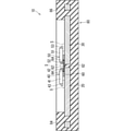
- FIG. 1 is a schematic plan view showing a circuit configuration according to the first embodiment.
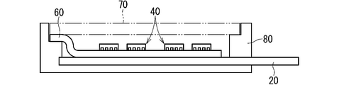
- FIG. 2 is a schematic cross-sectional view taken along line II-II of FIG.
- FIG. 3 is a partially enlarged view of FIG. It is a schematic plan view which the case is omitted in the circuit structure.
- FIG. 5 is a plan view showing a flexible wiring member.
- FIG. 6 is a plan view showing a modified example of the flexible wiring member.
- FIG. 7 is a schematic diagram showing a connection mode between the flexible wiring member and the control circuit board.
- FIG. 8 is a schematic diagram showing another connection mode between the flexible wiring member and the control circuit board.
- the circuit configuration of this disclosure is as follows.
- a first bus bar and a second bus bar constituting a power circuit, a first semiconductor element having a first power terminal, a second power terminal, and a first signal terminal, a third power terminal, a fourth power terminal, and a first signal terminal. Controls both a second semiconductor element having two signal terminals, a power circuit unit that electrically connects the first power terminal and the third power terminal, and both the first signal terminal and the second signal terminal.
- a control circuit unit for electrically connecting to the device is provided, the second power terminal is electrically connected to the first bus bar, and the first semiconductor element is mounted on the first bus bar.
- the fourth power terminal is electrically connected to the second bus bar, and the second semiconductor element is mounted on the second bus bar, so that at least one of the power circuit unit and the control circuit unit is used.
- the power circuit portion has a flexible conductive path, it is not necessary to use a bus bar as a member for electrically connecting the first power terminal and the third power terminal, and the weight of the circuit configuration can be reduced.
- both the first signal terminal and the second signal terminal are connected to one flexible conductive path, so that the first signal terminal and the second signal terminal are connected.
- the weight of the circuit configuration can be reduced as compared with the case where it is connected to separate flexible conductive paths.
- both the power circuit unit and the control circuit unit may have a flexible conductive path. This enhances the effect of reducing the weight of the circuit configuration.
- both the conductive path of the power circuit section and the conductive path of the control circuit section may be provided in one flexible wiring member. As a result, it is not necessary to provide a plurality of flexible wiring members, and cost reduction can be achieved.
- the conductive path of the control circuit section is provided along the outer edge of the flexible wiring member, and the conductive path of the control circuit section of the flexible wiring member is provided.
- the conductive path of the power circuit unit may be provided in the enclosed area.
- the conductive path of the power circuit section and the conductive path of the control circuit section can be provided on the one-layer flexible wiring member. As a result, it is not necessary to provide a plurality of layers of circuits in the flexible wiring member, and cost reduction can be achieved.
- an insulating spacer provided between the first bus bar and the second bus bar is further provided, and the flexible wiring member is from the first bus bar to the insulating spacer. It is arranged so as to extend beyond the second bus bar to the second bus bar, and the connection portion between the first power terminal and the power circuit unit and the connection portion between the first signal terminal and the control circuit unit are the first. It may be located on the bus bar, and the connection portion between the third power terminal and the power circuit unit and the connection portion between the second signal terminal and the control circuit unit may be located on the second bus bar. ..
- the flexible wiring member is deformed to absorb the displacement between the connecting portions, so that the electrical connection state at the connecting portion can be cut off. It is suppressed.
- any one of the circuit configurations (1) to (5) a plurality of sets of the first semiconductor element and the second semiconductor element are provided, and a plurality of sets of the first semiconductor element and the second semiconductor are provided.
- the first power terminal and the third power terminal in the element may be connected via one of the conductive paths. As a result, the electric resistance of the conductive path connecting the first power terminal and the third power terminal can be reduced, and the amount of heat generated when a large current flows can be suppressed.
- FIG. 1 is a schematic plan view showing a circuit configuration 10 according to the first embodiment.
- FIG. 2 is a schematic cross-sectional view taken along line II-II of FIG.
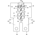
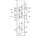
- FIG. 3 is a partially enlarged view of FIG.
- FIG. 4 is a schematic plan view of the circuit configuration 10 in which the case 80 is omitted.
- the circuit configuration 10 is mounted on a vehicle including, for example, a main system and a subsystem related to an automatic driving function.
- the circuit configuration 10 functions as, for example, a switching device that electrically disconnects the main system and the subsystem when the main system fails and switches to the subsystem.
- the circuit configuration 10 includes a first bus bar 20, a second bus bar 30, a first semiconductor element 40, a second semiconductor element 50, a power circuit unit, and a control circuit unit.
- the circuit configuration 10 is housed in the case 80.
- the first bus bar 20 and the second bus bar 30 form a power circuit.
- the first bus bar 20 and the second bus bar 30 are each formed in a plate shape by a conductive material such as copper or a copper alloy.
- the first bus bar 20 has a first element connecting portion 22 and a first external connecting portion 24.
- the second bus bar 30 has a second element connecting portion 32 and a second external connecting portion 34.
- the first element connecting portion 22 is a portion connected to the first semiconductor element 40.
- the second element connecting portion 32 is a portion connected to the second semiconductor element 50.
- the first external connection portion 24 and the second external connection portion 34 are portions to which the end portions of the wire harness and the like are connected.
- the first element connecting portion 22 and the second element connecting portion 32 are each formed in a flat plate shape and fit in the case 80.
- the first element connecting portion 22 and the second element connecting portion 32 are arranged so that the main surfaces are flush with each other while being spaced apart from each other.
- An insulating spacer 82 which will be described later, is provided between the first element connecting portion 22 and the second element connecting portion 32.
- the first external connection portion 24 and the second external connection portion 34 are each formed in a flat plate shape and project out of the case body that surrounds the first element connection portion 22 and the second element connection portion 32 in the case 80.
- through holes are formed in the first external connection portion 24 and the second external connection portion 34, respectively.
- the first external connection portion 24 and the second external connection portion 34 are bolted to the terminals of the wire harness using the through holes.
- Each of the first semiconductor element 40 and the second semiconductor element 50 is a semiconductor switching element that controls the on / off of current.
- a semiconductor switching element has two power terminals and a gate terminal.
- the on / off of the current between the two power terminals is controlled by controlling the on / off of the gate through the gate terminal.
- the semiconductor switching element cuts off the current flow from one power terminal side to the other power terminal side, while blocking the current flow from the other power terminal side to one power terminal side. Some flows cannot be completely blocked.
- the current whose on / off is controlled by such a semiconductor switching element is a large current, the current leaking from the other power terminal side to the one power terminal side when the gate is turned off may not be negligible.
- two semiconductor switching elements are connected in series so that the directions of the two power terminals are opposite to each other, thereby switching one of the semiconductors.
- the element cuts off the current in one direction
- the other semiconductor switching element cuts off the current in the other direction, so that the current in both directions can be cut off in the circuit configuration.
- Examples of such a semiconductor switching element include MOSFETs (Metal-Oxide-Semiconductor Field-Effect Transistor) and the like.
- the first semiconductor element 40 has a first power terminal 42, a second power terminal 43, and a first signal terminal 44.
- the first semiconductor element 40 is mounted on the first bus bar 20.
- the second semiconductor element 50 has a third power terminal 52, a fourth power terminal 53, and a second signal terminal 54.
- the second semiconductor element 50 is mounted on the second bus bar 30.
- the first power terminal 42 and the third power terminal 52 are electrically connected via a power circuit unit.
- the second power terminal 43 is electrically connected to the first bus bar 20, and the fourth power terminal 53 is electrically connected to the second bus bar 30.
- the first signal terminal 44 and the second signal terminal 54 are connected to the control device via the control circuit unit.
- the first semiconductor element 40 and the second semiconductor element 50 are MOSFETs
- the first power terminal 42 and the third power terminal 52 are source terminals
- the second power terminal 43 and the fourth power terminal 53 are drain terminals.
- the first signal terminal 44 and the second signal terminal 54 are gate terminals.
- the first power terminal 42 and the third power terminal 52 may be referred to as source terminals 42 and 52.
- the second power terminal 43 and the fourth power terminal 53 may be referred to as drain terminals 43 and 53
- the first signal terminal 44 and the second signal terminal 54 may be referred to as gate terminals 44 and 54.
- the terminal arrangement of the first semiconductor element 40 and the terminal arrangement of the second semiconductor element 50 are the same.
- a source terminal 42 and a gate terminal 44 are provided on one side surface of the main body 41, and a drain terminal 43 is provided on the other side surface.
- a source terminal 52 and a gate terminal 54 are provided on one side surface of the main body 51, and a drain terminal 53 is provided on the other side surface.
- the first semiconductor element 40 and the second semiconductor element 50 are arranged in opposite directions so that one side surface of the main body 41, 51 provided with the source terminals 42, 52 faces each other.
- the first semiconductor element 40 and the second semiconductor element 50 are arranged so as to be offset from each other in the direction in which the source terminals 42 and 52 and the gate terminals 44 and 54 are arranged so that the source terminals 42 and 52 face each other.
- the gate terminal 44 of the first semiconductor element 40 and the gate terminal 54 of the second semiconductor element 50 are located at different positions.
- the gate terminal 44 of the first semiconductor element 40 does not face the second semiconductor element 50.
- the gate terminal 54 of the second semiconductor element 50 does not face the first semiconductor element 40.
- the power circuit unit is a circuit unit that connects the first power terminal 42 and the third power terminal 52.
- the power circuit unit is provided with a connection portion with the first power terminal 42 and a connection portion with the third power terminal 52.
- the control circuit unit is a circuit unit for receiving a control signal from the control device or communicating with the control device and emitting an on / off signal to both the first signal terminal 44 and the second signal terminal 54. Yes, it may include a detection function such as current and voltage, and a safety function against a MOSFET failure.
- the control circuit unit is provided with a connection unit with the first signal terminal 44 and a connection unit with the second signal terminal 54.
- an ECU Electric Control Unit
- the control circuit unit is provided with a harness connection unit.
- At least one of the power circuit unit and the control circuit unit has flexible conductive paths 62 and 64.
- both the power circuit unit and the control circuit unit have flexible conductive paths 62 and 64.
- the flexible conductive path 62 of the power circuit section and the flexible conductive path 64 of the control circuit section are provided in one flexible wiring member 60.
- FIG. 5 is a plan view showing the flexible wiring member 60.
- the flexible wiring member 60 has flexible conductive paths 62 and 64 and an insulating portion 66.
- the conductive paths 62 and 64 are made of a conductor foil, a thin conductor plate, or the like.
- the insulating portion 66 is made of an insulating film or the like. Both the conductive paths 62 and 64 and the insulating portion 66 are easy to bend.
- the flexible wiring member 60 is an FPC (Flexible Printed Circuit Board).
- the insulating portion 66 of the FPC is a substrate main body made of, for example, a polyimide film. Conductive paths 62 and 64 made of copper foil or the like are provided on the substrate body.
- the flexible conductive paths 62 and 64 are, for example, conductive paths formed on a flexible substrate (flexible printed circuit board). In the FPC, the conductive paths 62 and 64 are exposed at each connection portion between the source terminal 42 of the first semiconductor element 40, the gate terminal 44, and the source terminal 52 and the gate terminal 54 of the second semiconductor element 50.
- the conductive paths 62 and 64 may be appropriately covered with a cover film or the like at a portion other than the connection portions of the semiconductor elements 40 and 50 with the terminals 42, 44, 52 and 54.
- the flexible wiring member 60 may be a member other than the FPC, for example, an FFC (Flexible Flat Cable) or the like.
- the power circuit unit has a conductive path 62
- the control circuit unit has a conductive path 64.
- a set of source terminals 42 and 52 is connected to the same conductive path 62. Therefore, the electric power circuit unit is substantially composed of only the conductive path 62, excluding the connecting member.
- the control circuit section further includes a control board circuit section provided on the control circuit board 70.
- the connection portion with the first signal terminal 44 and the connection portion with the second signal terminal 54 are provided in the conductive path 64, and the harness connection portion is provided in the control board circuit portion.
- connection mode in each connection portion between the terminals 42, 44, 52, 54 of the semiconductor elements 40 and 50 and the conductive paths 62, 64 is not particularly limited, and can be connected by, for example, solder S, terminals, or the like. .. 2 and 3 show how they are connected via the solder S.
- two conductive paths 62 and 64 are formed in one conductor layer.
- a part of the conductive path 64 is provided along the outer edge of the flexible wiring member 60.
- the conductive path 62 is provided in the region of the flexible wiring member 60 surrounded by the conductive path 62.
- the conductive path 62 is formed to have a size that can be connected to a set of the first semiconductor element 40 and the second semiconductor element 50. That is, one flexible wiring member has a plurality of conductive paths 62, and a plurality of sets of the first semiconductor element 40 and the second semiconductor element 50 are connected to different conductive paths 62, respectively.
- FIG. 6 is a plan view showing a modified example of the flexible wiring member 60.
- the flexible wiring member 160 is configured so that the source terminals 42 and 52 of the plurality of sets of the first semiconductor element 40 and the second semiconductor element 50 can be connected via one flexible conductive path 162.
- the conductive path 162 is formed longer in the parallel direction of the plurality of first semiconductor elements 40 as compared with the conductive path 62, and is formed in the plurality of (here, two) first semiconductor elements 40. Has a corresponding length. Then, two sets of the first semiconductor element 40 and the second semiconductor element 50 can be connected to one conductive path 162.
- four sets of the first semiconductor element 40 and the second semiconductor element 50 are separated into two sets and can be connected to different conductive paths 162.
- the four sets of the first semiconductor element 40 and the second semiconductor element 50 may be made connectable to a flexible conductive path for one power circuit unit.
- the insulating spacer 82 partitions between the first bus bar 20 and the second bus bar 30.
- the insulating spacer 82 is part of the case 80.
- the flexible wiring member 60 is arranged so as to extend from the first bus bar 20 to the second bus bar 30 beyond the insulating spacer 82.
- the connection portion between the source terminal 42 and the conductive path 62 and the connection portion between the gate terminal 44 and the conductive path 64 are located on the first bus bar 20.
- the connection portion between the source terminal 52 and the conductive path 62 and the connection portion between the gate terminal 54 and the conductive path 64 are located on the second bus bar 30.
- the control circuit board 70 has a substrate main body formed of an insulating material and a control board circuit portion formed of a conductive material.
- the control circuit board 70 is assumed to be a printed circuit board whose main body is a rigid type, but may be a printed circuit board whose main body is a flexible type.
- the control board circuit unit is provided with a connection unit connected to the conductive path 64.
- the control circuit board 70 may be provided with a connector 72 as a harness connection portion.
- the connector 72 has a connector housing made of an insulating resin and a connector terminal for electrically connecting a control circuit board and an external conductor.
- the control circuit board 70 may be fixed to, for example, the case 80 or the bus bars 20 and 30.
- the control circuit board 70 may be supported by the case 80 at intervals from the bus bars 20 and 30.
- the case 80 is formed of an insulating resin as a material.
- the case 80 is a molded product in which the first bus bar 20 and the second bus bar 30 are insert-molded as insert parts.
- the case 80 has an insulating spacer 82, a first bus bar holding portion 84, and a second bus bar holding portion 86.
- the insulating spacer 82 is provided between the first bus bar 20 and the second bus bar 30, and is a portion that partitions the first bus bar 20 and the second bus bar 30.
- One side surface of the insulating spacer 82 is in contact with the first bus bar 20, and the other side surface is in contact with the second bus bar 30.
- the upper surface of the insulating spacer 82 may be formed flush with the main surface of the first bus bar 20 and the main surface of the second bus bar 30.
- the first bus bar holding portion 84 is a portion that holds the first bus bar 20. Of the first bus bar 20, the outer edge portion on the side opposite to the outer edge portion in contact with the insulating spacer 82 is held by the first bus bar holding portion 84. Further, in the first bus bar 20, the connecting portion between the first element connecting portion 22 and the first external connecting portion 24 is held by the first bus bar holding portion 84.
- the second bus bar holding portion 86 is a portion that holds the second bus bar 30. Of the second bus bar 30, the outer edge portion on the side opposite to the outer edge portion in contact with the insulating spacer 82 is held by the second bus bar holding portion 86.
- the connecting portion between the second element connecting portion 32 and the second external connecting portion 34 is held by the second bus bar holding portion 86.
- the first bus bar holding portion 84 holds the first bus bar 20 by sandwiching it in the thickness direction.
- the second bus bar holding portion 86 holds the second bus bar 30 by sandwiching it in the thickness direction.
- a through hole 25 is formed in a portion of the first bus bar 20 that is held by the first bus bar holding portion 84.
- a portion of the first bus bar holding portion 84 that covers one side and a portion that covers the other side of the first bus bar 20 are connected to each other through a connecting portion in the through hole 25.
- a through hole 35 is formed in a portion of the second bus bar 30 that is held by the second bus bar holding portion 86. Also in the second bus bar holding portion 86, the portion covering one side and the portion covering the other side of the second bus bar 30 are connected to each other through the connecting portion in the through hole 35.
- the case 80 may be provided with a fixing portion for fixing the control circuit board 70, a fixing portion for fixing the cover, and the like.
- a fixing portion may be, for example, a screw hole.
- the fixing portion may be either a locking convex portion or a locking concave portion used in the locking structure with the mating side member.
- the conductive path 64 of the flexible wiring member 60 is connected to the control board circuit portion of the control circuit board 70 on the other end side.
- FIG. 7 is a schematic diagram showing a connection mode between the flexible wiring member 60 and the control circuit board 70.
- FIG. 8 is a schematic diagram showing another connection mode between the flexible wiring member 60 and the control circuit board 70.
- the flexible wiring member 60 may be bent in the thickness direction at one end thereof while being in contact with the bus bars 20 and 30 and at the other end in contact with the control circuit board 70.
- the flexible wiring member 60 may be folded back in the thickness direction between one end and the other end.
- the flexible wiring member 60 may be bent between one end and the other end without being folded back in the thickness direction.
- the flexible wiring member 60 may not be folded or bent in the thickness direction between one end and the other end.
- the conductive path 64 and the control board circuit unit can be connected via, for example, solder, terminals, connectors, or the like.
- the flexible wiring member 60 and the control circuit board 70 may be connected without being in contact with each other.
- a terminal provided on either one of the flexible wiring member 60 and the control circuit board 70 extends to either one, and the flexible wiring member 60 and the control circuit board 70 are connected via the terminal. You may.
- At least one of a power circuit unit for electrically connecting the source terminals 42 and 52 and a control circuit unit for electrically connecting both the gate terminals 44 and 54 to the control device is a conductive path 62 or 64.
- both the power circuit unit and the control circuit unit have conductive paths 62 and 64.
- the bus bar does not need to be used as a member for electrically connecting the source terminals 42 and 52, and the weight of the circuit configuration 10 can be reduced.
- the gate terminals 44 and 54 are connected to one conductive path 64 by connecting both the gate terminals 44 and 54 to one conductive path 64, so that the gate terminals 44 and 54 are connected to different conductive paths. In comparison, the weight of the circuit configuration 10 can be reduced.
- both the conductive path 62 of the power circuit section and the conductive path 64 of the control circuit section are provided in one flexible wiring member 60. As a result, it is not necessary to provide a plurality of flexible wiring members 60, and cost reduction can be achieved.
- a conductive path 64 of the control circuit section is provided along the outer edge of the flexible wiring member 60, and the conductive path 62 of the power circuit section is provided in a region of the flexible wiring member 60 surrounded by the conductive path 64 of the control circuit section. Is provided.
- the power circuit unit and the control circuit unit can be provided on the one-layer flexible wiring member 60. It is not necessary to provide a plurality of layers of conductive paths in the flexible wiring member 60, and cost reduction can be achieved.
- the flexible wiring member 60 is arranged so as to extend from the first bus bar 20 to the second bus bar 30 beyond the insulating spacer 82, the connection portion between the source terminal 42 and the power circuit portion, and the gate terminal 44 and the control circuit.
- the connection portion with the unit is located on the first bus bar 20, the connection portion between the source terminal 52 and the power circuit unit, and the connection portion between the gate terminal 54 and the control circuit unit are located on the second bus bar 30. ..
- the source terminals 42 and 52 of the plurality of sets of the first semiconductor element 40 and the second semiconductor element 50 are connected via one conductive path 162.
- the electric resistance of the conductive path 162 connecting the source terminals 42 and 52 can be reduced, and the amount of heat generated when a large current flows can be suppressed.
- both the power circuit unit and the control circuit unit have conductive paths 62 and 64, but this is not an essential configuration.
- the power circuit unit and the control circuit unit only the power circuit unit may have the conductive path 62, or only the control circuit unit may have the conductive path 64.
- the gate terminals 44 and 54 are directly connected to the control circuit board 70 via the terminals provided on the control circuit board 70 without passing through the conductive path 64. May be connected.
- the control circuit portion has the conductive path 64, for example, even if the source terminals 42 and 52 are connected via a third bus bar provided separately from the first bus bar 20 and the second bus bar 30. good.
- one flexible wiring member 60 is provided with a conductive path 62 of a power circuit section and a conductive path 64 of a control circuit section, but this is not an essential configuration.
- a flexible wiring member having a conductive path 62 for the power circuit section and a flexible wiring member having a conductive path 64 for the control circuit section may be provided separately.
- One flexible wiring member 60 may have a plurality of conductive layers, and the conductive path of the power circuit section and the conductive path of the control circuit section may be provided in another conductive layer.
Landscapes
- Engineering & Computer Science (AREA)
- Microelectronics & Electronic Packaging (AREA)
- Power Conversion In General (AREA)
- Connection Or Junction Boxes (AREA)
Priority Applications (2)
| Application Number | Priority Date | Filing Date | Title |
|---|---|---|---|
| US18/043,672 US12490383B2 (en) | 2020-09-03 | 2021-08-03 | Circuit assembly |
| CN202180050249.1A CN115956294A (zh) | 2020-09-03 | 2021-08-03 | 电路结构体 |
Applications Claiming Priority (2)
| Application Number | Priority Date | Filing Date | Title |
|---|---|---|---|
| JP2020148266A JP7533036B2 (ja) | 2020-09-03 | 2020-09-03 | 回路構成体 |
| JP2020-148266 | 2020-09-03 |
Publications (1)
| Publication Number | Publication Date |
|---|---|
| WO2022049963A1 true WO2022049963A1 (ja) | 2022-03-10 |
Family
ID=80491118
Family Applications (1)
| Application Number | Title | Priority Date | Filing Date |
|---|---|---|---|
| PCT/JP2021/028691 Ceased WO2022049963A1 (ja) | 2020-09-03 | 2021-08-03 | 回路構成体 |
Country Status (4)
| Country | Link |
|---|---|
| US (1) | US12490383B2 (https=) |
| JP (2) | JP7533036B2 (https=) |
| CN (1) | CN115956294A (https=) |
| WO (1) | WO2022049963A1 (https=) |
Citations (2)
| Publication number | Priority date | Publication date | Assignee | Title |
|---|---|---|---|---|
| JP2010022117A (ja) * | 2008-07-09 | 2010-01-28 | Autonetworks Technologies Ltd | 回路構成体 |
| WO2018086338A1 (zh) * | 2016-11-12 | 2018-05-17 | 深圳市易特科信息技术有限公司 | 带有十二导联心电监测仪的健康监测一体机 |
Family Cites Families (6)
| Publication number | Priority date | Publication date | Assignee | Title |
|---|---|---|---|---|
| DE102009046258B3 (de) * | 2009-10-30 | 2011-07-07 | Infineon Technologies AG, 85579 | Leistungshalbleitermodul und Verfahren zum Betrieb eines Leistungshalbleitermoduls |
| JP2016220277A (ja) | 2015-05-14 | 2016-12-22 | 矢崎総業株式会社 | 電気接続箱 |
| JP2019096769A (ja) | 2017-11-24 | 2019-06-20 | 株式会社オートネットワーク技術研究所 | 回路構成体 |
| JP6939542B2 (ja) * | 2017-12-28 | 2021-09-22 | 株式会社オートネットワーク技術研究所 | 電気接続装置 |
| JP2020013896A (ja) | 2018-07-18 | 2020-01-23 | 株式会社オートネットワーク技術研究所 | 回路基板 |
| US11183440B2 (en) * | 2018-12-10 | 2021-11-23 | Gan Systems Inc. | Power modules for ultra-fast wide-bandgap power switching devices |
-
2020
- 2020-09-03 JP JP2020148266A patent/JP7533036B2/ja active Active
-
2021
- 2021-08-03 WO PCT/JP2021/028691 patent/WO2022049963A1/ja not_active Ceased
- 2021-08-03 CN CN202180050249.1A patent/CN115956294A/zh active Pending
- 2021-08-03 US US18/043,672 patent/US12490383B2/en active Active
-
2024
- 2024-06-21 JP JP2024100395A patent/JP7722528B2/ja active Active
Patent Citations (2)
| Publication number | Priority date | Publication date | Assignee | Title |
|---|---|---|---|---|
| JP2010022117A (ja) * | 2008-07-09 | 2010-01-28 | Autonetworks Technologies Ltd | 回路構成体 |
| WO2018086338A1 (zh) * | 2016-11-12 | 2018-05-17 | 深圳市易特科信息技术有限公司 | 带有十二导联心电监测仪的健康监测一体机 |
Also Published As
| Publication number | Publication date |
|---|---|
| US20230354526A1 (en) | 2023-11-02 |
| CN115956294A (zh) | 2023-04-11 |
| JP2022042712A (ja) | 2022-03-15 |
| US12490383B2 (en) | 2025-12-02 |
| JP7533036B2 (ja) | 2024-08-14 |
| JP7722528B2 (ja) | 2025-08-13 |
| JP2024111245A (ja) | 2024-08-16 |
Similar Documents
| Publication | Publication Date | Title |
|---|---|---|
| CN110707273B (zh) | 保护器及汇流条模块 | |
| CN108463375B (zh) | 电路结构体 | |
| CN113169402A (zh) | 布线部件及电池模块 | |
| US7504926B2 (en) | Fuse module | |
| CN110707272B (zh) | 装配有连接器的电路体以及汇流条模块 | |
| US10964929B2 (en) | Structure of connection among circuit body, bus bar and electronic element | |
| JP2016220277A (ja) | 電気接続箱 | |
| US11458913B2 (en) | Wiring module including a power supply branch part | |
| CN108353501A (zh) | 电路结构体 | |
| JP6764389B2 (ja) | 半導体モジュールユニット | |
| CN113906832B (zh) | 基板结构体 | |
| WO2022049963A1 (ja) | 回路構成体 | |
| CN112425018A (zh) | 电接线盒 | |
| CN109937159A (zh) | 布线模块及布线模块中的连接构件 | |
| CN113728526B (zh) | 布线基板 | |
| US12604411B2 (en) | Flexible printed circuit board, in particular for connecting electrical and/or electronic components | |
| JP7677118B2 (ja) | 回路構成体 | |
| JP2006004852A (ja) | 電子部品内蔵コネクタ | |
| CN112514542A (zh) | 电路基板 | |
| CN112368834A (zh) | 电路基板 | |
| JP2026063667A (ja) | 電気接続ユニット | |
| WO2024185072A1 (ja) | 回路体 | |
| WO2024166314A1 (ja) | 回路体 | |
| JP2004241145A (ja) | フラットケーブル構造 |
Legal Events
| Date | Code | Title | Description |
|---|---|---|---|
| 121 | Ep: the epo has been informed by wipo that ep was designated in this application |
Ref document number: 21864021 Country of ref document: EP Kind code of ref document: A1 |
|
| NENP | Non-entry into the national phase |
Ref country code: DE |
|
| 122 | Ep: pct application non-entry in european phase |
Ref document number: 21864021 Country of ref document: EP Kind code of ref document: A1 |