WO2024166314A1 - 回路体 - Google Patents
回路体 Download PDFInfo
- Publication number
- WO2024166314A1 WO2024166314A1 PCT/JP2023/004413 JP2023004413W WO2024166314A1 WO 2024166314 A1 WO2024166314 A1 WO 2024166314A1 JP 2023004413 W JP2023004413 W JP 2023004413W WO 2024166314 A1 WO2024166314 A1 WO 2024166314A1
- Authority
- WO
- WIPO (PCT)
- Prior art keywords
- pair
- terminal
- bus bars
- conductor pattern
- mounting portion
- Prior art date
- Legal status (The legal status is an assumption and is not a legal conclusion. Google has not performed a legal analysis and makes no representation as to the accuracy of the status listed.)
- Ceased
Links
Images


Classifications
-
- H—ELECTRICITY
- H01—ELECTRIC ELEMENTS
- H01L—SEMICONDUCTOR DEVICES NOT COVERED BY CLASS H10
- H01L25/00—Assemblies consisting of a plurality of semiconductor or other solid state devices
- H01L25/03—Assemblies consisting of a plurality of semiconductor or other solid state devices all the devices being of a type provided for in a single subclass of subclasses H10B, H10D, H10F, H10H, H10K or H10N, e.g. assemblies of rectifier diodes
- H01L25/04—Assemblies consisting of a plurality of semiconductor or other solid state devices all the devices being of a type provided for in a single subclass of subclasses H10B, H10D, H10F, H10H, H10K or H10N, e.g. assemblies of rectifier diodes the devices not having separate containers
- H01L25/07—Assemblies consisting of a plurality of semiconductor or other solid state devices all the devices being of a type provided for in a single subclass of subclasses H10B, H10D, H10F, H10H, H10K or H10N, e.g. assemblies of rectifier diodes the devices not having separate containers the devices being of a type provided for in group subclass H10D
-
- H—ELECTRICITY
- H01—ELECTRIC ELEMENTS
- H01L—SEMICONDUCTOR DEVICES NOT COVERED BY CLASS H10
- H01L25/00—Assemblies consisting of a plurality of semiconductor or other solid state devices
- H01L25/18—Assemblies consisting of a plurality of semiconductor or other solid state devices the devices being of the types provided for in two or more different main groups of the same subclass of H10B, H10D, H10F, H10H, H10K or H10N
Definitions
- This disclosure relates to a circuit body.
- Patent Document 1 discloses an electrical junction box that includes a pair of bus bars that form a current path between a power source and a load, and a cutoff unit that is mounted on the pair of bus bars and is made up of power semiconductors that pass or cut off current between the bus bars.
- Patent Document 1 a pair of power terminals (drain terminal and source terminal) of the interrupter are mounted on a pair of bus bars, respectively, and a control terminal (gate terminal) of the interrupter is mounted on a conductor pattern of a flexible printed circuit board placed on the bus bar. Therefore, due to the difference in height between the control terminal and the pair of power terminals when mounted, the interrupter is mounted at an angle, and there is a risk of connection failure due to misalignment of the control terminal from the conductor pattern.
- the circuit body of the present disclosure includes a pair of bus bars that form a current path between two conductive paths, a printed circuit board that is placed on at least one of the surfaces of the pair of bus bars and has a conductor pattern connected to a control circuit exposed on the board surface, a pair of power terminals that are respectively mounted on the surfaces of the pair of bus bars, and a control terminal that is mounted on the conductor pattern, and a cut-off section that allows and cuts off current between the pair of bus bars, and at least one of the pair of power terminals has a mounting section that is mounted on the board surface of the printed circuit board.
- a circuit body includes a pair of bus bars forming a current path between two conductive paths, a printed circuit board placed on at least one of the surfaces of the pair of bus bars and having a conductor pattern connected to a control circuit exposed on the surface of the board, a pair of power terminals respectively mounted on the surfaces of the pair of bus bars, and a control terminal mounted on the conductor pattern, and a breaker section that passes and breaks current between the pair of bus bars, and a housing portion of a main body of the breaker section forms a mounting section that is placed on the board surface of the printed circuit board.
- the circuit body disclosed herein can suppress inclination of the interrupter when it is mounted on a pair of bus bars and the conductor pattern of a printed circuit board placed on the bus bars.
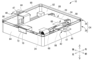
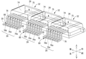
- FIG. 1 is a perspective view showing a circuit body according to a first embodiment with a part of a case being see-through.
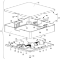
- FIG. FIG. 2 is a partially exploded perspective view showing a part of the circuit body shown in FIG. 1 in an exploded state.
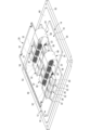
- FIG. 3 is an enlarged perspective view showing a main part of the circuit body shown in FIG. 1 with a control board seen through.
- FIG. 4 is a plan view of a main portion of the circuit body shown in FIG.
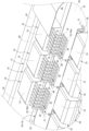
- FIG. 5 is a perspective view showing, on a further enlarged scale, a main portion of the circuit body shown in FIG.
- FIG. 6 is a perspective view showing the interrupter constituting the circuit body shown in FIG. 1 with the main body part seen through.
- FIG. 7 is an enlarged perspective view showing a main part of a circuit body according to the second embodiment, and corresponds to FIG.
- FIG. 8 is an enlarged perspective view showing a main part of a circuit body according to the third embodiment, and corresponds to FIG.
- FIG. 9 is a perspective view showing, on a further enlarged scale, the main part of the circuit body shown in FIG. 8, and corresponds to FIG.
- FIG. 10 is an enlarged perspective view showing a main part of a circuit body according to the fourth embodiment, and corresponds to FIG.
- the circuit body of the present disclosure comprises: (1) A device comprising: a pair of bus bars forming a current path between two conductive paths; a printed circuit board placed on at least one of the surfaces of the pair of bus bars and having a conductor pattern connected to a control circuit exposed on the surface of the board; a pair of power terminals mounted on the surfaces of the pair of bus bars, respectively; and a control terminal mounted on the conductor pattern, and a cut-off unit for passing and cutting off current between the pair of bus bars, wherein at least one of the pair of power terminals has a mounting portion that is mounted on the board surface of the printed circuit board.
- a pair of power terminals of the interrupter are mounted on the surfaces of the pair of bus bars, respectively, and a control terminal of the interrupter is mounted on at least one of the surfaces of the pair of bus bars and on a conductor pattern exposed on the surface of a printed circuit board located above the pair of bus bars.
- At least one of the pair of power terminals has a mounting portion that is placed on the board surface of the printed circuit board.
- the number of terminals mounted on the bus bar at a low height position is greater than the number of terminals mounted on the conductor pattern at a high height position, so that the interrupter is easily drawn toward the bus bar during mounting, and there was a risk of the interrupter being inclined so that the control terminal side is raised.
- at least one of the pair of power terminals has a mounting portion that is placed on the board surface of the printed circuit board at a height position higher than the pair of bus bars. Therefore, by increasing the area that is held at the height of the printed circuit board during mounting, the inclination of the interrupter during mounting can be reduced compared to conventional structures.
- the mounting portion only needs to be provided on at least one of the pair of power terminals, and can be provided in any desired location and shape depending on the routing path of the busbar or conductor.
- one of the pair of power terminals is connected to one of the pair of bus bars connected to one of the two conductive paths
- the other of the pair of power terminals is connected to the other of the pair of bus bars connected to the other of the two conductive paths
- the other of the power terminals includes a plurality of terminal fittings, at least one of the terminal fittings constitutes the mounting portion placed on the surface of the substrate, and the remaining terminal fittings are mounted on the other of the pair of bus bars.
- the other power terminal of an interrupter constituted by a power semiconductor or the like such as a source terminal mounted on the other bus bar connected to the other of the two conductive paths
- at least one of the multiple terminal fittings can be advantageously used to constitute a mounting part to be placed on the surface of the printed circuit board.
- the conductive resistance can be reduced by securing a conductive path using multiple terminal fittings.
- At least one of the terminal fittings constituting the mounting portion is connected to the conductor pattern.
- the at least one terminal fittings constituting the mounting portion is not connected to the conductor pattern. Since the at least one terminal fitting used in the mounting portion is a so-called dummy terminal that is not connected to the conductor pattern of the printed circuit board, when selecting the at least one terminal fitting to be used as the mounting portion, there is no restriction on the wiring location of the conductor pattern. Therefore, there is an advantage in that a terminal fitting arranged in a position that further corrects the inclination of the interrupter when mounted can be advantageously selected. For example, by selecting the terminal fitting arranged in a position farthest from the control terminal as the mounting portion, the inclination of the interrupter when mounted can be further advantageously suppressed.
- the terminal fittings are arranged in parallel with the control terminal, and the mounting portion is configured to include the terminal fitting that is the furthest from the control terminal in the parallel direction.
- the mounting portion is configured to include the terminal fitting that is the furthest from the control terminal in the parallel direction among the terminal fittings arranged in parallel with the control terminal, it is possible to more reliably suppress the inclination of the interrupter during mounting.
- the printed circuit board is placed on the surface of the other of the pair of bus bars, the surface of the other of the pair of bus bars is partially exposed through a through hole provided in the printed circuit board, the control terminal mounted on the conductor pattern and at least one of the terminal fittings constituting the mounting portion are placed around the through hole in the printed circuit board, and the other terminal fittings are mounted on the surface exposed through the through hole.
- one of the pair of power terminals is connected to one of the pair of bus bars connected to one of the two conductive paths, and the other of the pair of power terminals is connected to the other of the pair of bus bars connected to the other of the two conductive paths, one of the power terminals includes a flat terminal fitting, a part of the flat terminal fitting constitutes the mounting portion placed on the substrate surface, and another part of the flat terminal fitting is mounted on one of the pair of bus bars.
- a cutoff section formed of a power semiconductor or the like has one power terminal, such as a drain terminal mounted on one bus bar connected to one of two conductive paths, formed of a flat terminal fitting.
- a mounting part to be placed on the surface of the printed circuit board can be advantageously formed by extending a part of the flat terminal fitting toward the printed circuit board and/or by extending the printed circuit board toward the flat terminal fitting.
- the flat terminal fittings are often disposed on the underside of the case of the cutoff section, and by making good use of the dead space on the underside of the case and simply extending a part of the flat terminal fitting toward the printed circuit board or extending the printed circuit board toward the flat terminal fitting, it is possible to easily provide a mounting part in a space-efficient manner.
- a circuit body includes: (8) A circuit breaker including a pair of bus bars forming a current path between two conductive paths, a printed circuit board placed on at least one of the surfaces of the pair of bus bars and having a conductor pattern connected to a control circuit exposed on the surface of the board, and a pair of power terminals mounted on the surfaces of the pair of bus bars, respectively, and a control terminal mounted on the conductor pattern, and which performs current flow and cut-off between the pair of bus bars, wherein a housing portion of a main body of the circuit breaker forms a mounting portion that is placed on the board surface of the printed circuit board.
- the housing portion of the main body of the interrupter constitutes a mounting portion that is placed on the surface of the printed circuit board. Therefore, as in the above embodiment (1), the area that is held at the height of the printed circuit board during mounting is increased, making it possible to suppress tilting of the interrupter during mounting compared to conventional structures.
- the electric junction box 10 is an example of a circuit body.
- the electric junction box 10 is disposed between two conductive paths, a high-voltage battery and a high-voltage load, in a vehicle such as an electric vehicle or a hybrid vehicle, to pass or cut off electricity between them.
- the electric junction box 10 can be disposed in any orientation, but in the following description, the up-down, front-rear, and left-right directions refer to the up-down, front-rear, and left-right directions shown in Fig. 1, respectively.
- the members may be labeled with a reference symbol, and the reference symbols may be omitted for the other members.
- the electrical junction box 10 includes a pair of bus bars (a drain-side bus bar 12 and a source-side bus bar 14) that are arranged at approximately the same height and that form a current path between a power source (e.g., a high-voltage battery) as one of two conductive paths (not shown) and a load (e.g., a high-voltage load) as the other of the two conductive paths.
- a power source e.g., a high-voltage battery
- a load e.g., a high-voltage load
- the electrical junction box 10 also includes a flexible printed circuit board (hereinafter, FPC) 24 that is placed on at least one of the surfaces (a drain-side surface 16 and a source-side surface 18) of the pair of bus bars (the drain-side bus bar 12 and the source-side bus bar 14) and that serves as a printed circuit board on which a conductor pattern 21 (shown by a two-dot chain line in FIG. 5 ) that is connected to a control circuit (not shown) provided on a control board 20 is exposed on a board surface 22.
- FPC flexible printed circuit board
- the electrical junction box 10 includes a pair of power terminals (drain terminal 26 and source terminal 28) mounted on the surfaces (drain side surface 16 and source side surface 18) of the pair of bus bars (drain side bus bar 12 and source side bus bar 14), respectively, and a control terminal 30 mounted on the conductor pattern 21, and is provided with a cut-off section 32 that passes and cuts off electricity between the pair of bus bars (drain side bus bar 12 and source side bus bar 14).
- a case 34 is provided to house a pair of bus bars (the drain side bus bar 12 and the source side bus bar 14), the control board 20, the FPC 24, and the cutoff section 32.
- the case 34 is configured to include an upper case 36 and a lower case 38.
- a drain side end bus bar 40 is connected to the drain side bus bar 12, and a source side end bus bar 42 is connected to the source side bus bar 14. The end of the drain side end bus bar 40 opposite to the side connected to the drain side bus bar 12 protrudes to the outside of the case 34 as a drain side external connection part 44.
- the end of the source side end bus bar 42 opposite to the side connected to the source side bus bar 14 protrudes to the outside of the case 34 as a source side external connection part 46.
- the drain side and source side external connection parts 44, 46 each have a through hole 47 penetrating in the thickness direction.
- the drain-side busbar 12 which is one of the pair of busbars, is a metal plate having a generally E-shape and is made of a metal having excellent electrical conductivity, such as copper (including copper alloys) or aluminum (including aluminum alloys).
- the E-shaped opening of the drain-side busbar 12 is disposed so as to face forward. That is, a connecting portion 48 extending in the left-right direction is provided at the rear of the drain-side busbar 12, and drain-side connecting portions 50 to which the aforementioned drain terminal 26 is connected extend forward from both left-right ends and the left-right center of the connecting portion 48.
- the drain side busbar 12 has drain side connection parts 50 extending in the front-rear direction at both left-right ends and the left-right center, and the rear ends of the drain side connection parts 50 are connected by the connection parts 48.
- a front opening 52 that opens forward is formed between each drain side connection part 50 at both left-right ends and the left-right center of the drain side busbar 12.
- the drain side end busbar 40 described above is fixed to the connection parts 48 of the drain side busbar 12 by, for example, welding.
- the drain side external connection parts 44 of the drain side end busbar 40 are connected to a power source side electric wire, busbar, etc. (not shown) with or without using the through holes 47.
- the source-side busbar 14 which is the other of the pair of busbars, is a generally U-shaped metal plate and is made of a metal having excellent electrical conductivity, such as copper (including copper alloys) or aluminum (including aluminum alloys).
- the U-shaped opening of the source-side busbar 14 is disposed so as to face rearward. That is, a connecting portion 54 extending in the left-right direction is provided at the front of the source-side busbar 14, and source-side connecting portions 56 to which the above-mentioned source terminals 28 are connected extend rearward from both left-right ends of the connecting portion 54.
- the source side busbar 14 has source side connection parts 56 extending in the front-rear direction at both left-right ends, and the front ends of the source side connection parts 56 are connected by the connecting parts 54.
- a rear opening 58 that opens toward the rear is formed in the left-right center of the source side busbar 14.
- the source side end busbar 42 described above is fixed to the connecting parts 54 of the source side busbar 14 by, for example, welding.
- the source side external connection parts 46 of the source side end busbar 42 are connected to a load side electric wire, busbar, etc. (not shown) with or without using the through holes 47.
- the drain side busbar 12 and the source side busbar 14 have approximately the same thickness dimension, and when fixed onto the adhesive sheet 60 and the bottom plate 62 described below, the height positions (vertical positions) of the drain side surface 16 and the source side surface 18 are approximately the same.
- the drain side busbar 12 and the source side busbar 14 are bonded to a metal bottom plate 62 via, for example, a substantially rectangular adhesive sheet 60.
- the drain side busbar 12 and the source side busbar 14 are arranged to face each other in the front-rear direction, with the source side busbar 14 provided in front of the adhesive sheet 60 and the drain side busbar 12 provided behind the adhesive sheet 60.
- the drain side connection portion 50 at the center of the drain side busbar 12 in the left-right direction is arranged in the rear opening 58 of the source side busbar 14.
- each source side connection portion 56 at both ends of the source side busbar 14 in the left-right direction is arranged in each front opening 52 of the drain side busbar 12.
- each drain side connection portion 50 and each source side connection portion 56 are alternately arranged in the left-right direction.
- Each drain side connection portion 50 and each source side connection portion 56 face each other at a predetermined distance in the left-right direction.
- the adhesive sheet 60 is preferably insulating and thermally conductive, and may be a conventionally known thermally conductive sheet.
- the adhesive sheet 60 may be made of, for example, polyethylene terephthalate (PET), polyethylene naphthalate (PEN), polytetrafluoroethylene (PTFE), polycarbonate (PC), polyimide (PI), or the like. That is, the adhesive sheet 60 is made of, for example, a synthetic resin having a higher thermal conductivity than air. Specifically, silicone-based resins, non-silicone acrylic resins, ceramic resins, and the like may be used. More specifically, examples of the adhesive sheet 60 include heat dissipation gap fillers, heat conductive greases, and heat conductive silicone rubbers, all made of silicone-based resins. In the first embodiment, the adhesive sheet 60 is in the form of a sheet, but this is not limited to this and any shape may be used.
- the bottom plate 62 is formed to a size sufficient to cover a lower opening 92 of the lower case 38, which will be described later, and is fixed to the lower case 38 with screws 64.
- heat generated in the interrupter 32 and the like can be dissipated through the drain and source side bus bars 12, 14, the adhesive sheet 60, the bottom plate 62, and, for example, through a metal housing (not shown) on which the electrical junction box 10 is placed.
- the adhesive sheet 60 does not need to be provided, and the drain and source side bus bars 12, 14 and the bottom plate 62 can be fixed by a conventionally known fixing method, such as bolt fixing.
- FPC24 ⁇ Printed circuit board (FPC24)> An FPC 24 serving as a printed circuit board is placed on a surface (source-side surface 18) of the source-side bus bar 14, which is the other of the pair of bus bars. A conductor pattern 21 is printed on a board surface 22 of the FPC 24, and the conductor pattern 21 is exposed on the board surface 22.
- each FPC 24 is substantially strip-shaped.
- One end of each FPC 24 in the length direction is placed on each source side connection part 56 of the source side bus bar 14 and fixed by adhesive or the like.
- one end of each FPC 24 in the length direction is overlapped and fixed over substantially the entire surface of each source side connection part 56.
- a substantially rectangular through hole 66 is formed corresponding to the position of the source terminal 28 in the interrupter 32.
- a plurality of interrupters 32 are provided as described below, a plurality of through holes 66 are formed in each FPC 24, and the source side surface 18 of the source side bus bar 14 is partially exposed through these through holes 66.
- a folded portion 68 is provided in the middle of the length of each FPC 24, and the other end of each FPC 24 is folded upward from the one end of each FPC 24 placed on each source side connection portion 56.
- a control board 20 on which a control circuit (not shown) is printed is fixed to the other end of each FPC 24, and the conductor pattern 21 of each FPC 24 and the control circuit on the control board 20 are electrically connected.
- a connector 70 is mounted on the control board 20, and the control circuit on the control board 20 and the connector 70 are electrically connected. When the electrical connection box 10 is assembled, the connector 70 is exposed to the outside through an opening 72 provided in the case 34. Then, by connecting an external device (not shown) to the connector 70, signals from the external device are transmitted to the cutoff portion 32 through the control circuit on the control board 20 and the conductor pattern 21 on each FPC 24.
- a cutoff unit 32 that passes and cuts off current between the drain side bus bar 12 and the source side bus bar 14 is connected to the drain side connection unit 50 of the drain side bus bar 12 and the source side connection unit 56 of the source side bus bar 14.
- the cutoff unit 32 is a power MOSFET (Metal-Oxide-Semiconductor Field-Effect Transistor), which is a power semiconductor.
- MOSFET Metal-Oxide-Semiconductor Field-Effect Transistor
- a plurality of cutoff units 32 are provided across the drain side connection unit 50 and the source side connection unit 56 that face each other at a predetermined distance in the left-right direction, and these multiple cutoff units 32 are arranged in parallel in the front-rear and left-right directions.
- each interrupter 32 has a pair of power terminals, a drain terminal 26, a source terminal 28, and a control terminal 30.
- the drain terminal 26, source terminal 28, and control terminal 30 are provided to protrude outward from a roughly rectangular block-shaped main body 74 that constitutes the interrupter 32. Since a conventionally known power MOSFET can be used as each interrupter 32, the specific structure of the main body 74 will not be described. For ease of understanding, FIG. 6 shows the main body 74 in a see-through manner.
- the drain terminal 26, which is one of the power terminals in each interrupter 32, includes a roughly plate-shaped flat terminal fitting 75.
- This drain terminal 26 (flat terminal fitting 75) forms a wide area on the bottom surface (lower surface) of the main body 74, and protrudes outward from the main body 74 (for example, in the direction of the arrow pointing to the right in each interrupter 32 shown in Figure 6).
- the source terminal 28, which is the other power terminal in each interrupter 32, is configured to include a plurality of terminal fittings 76.
- the plurality of terminal fittings 76 constituting this source terminal 28 protrude outward from the main body 74 on the opposite side to the drain terminal 26 (for example, in the direction of the arrow indicating the left in each interrupter 32 shown in FIG. 6), and these plurality of terminal fittings 76 are arranged in parallel.
- six terminal fittings 76 are arranged side by side in the direction of the arrow indicating the front-to-rear direction.
- each terminal fitting 76 is not limited, but in the first embodiment, each terminal fitting 76 is gull-wing shaped, bent into a substantially L-shape, and a vertical portion 78 extending up and down is provided at the longitudinal middle portion of each terminal fitting 76. That is, each terminal metal fitting 76 protrudes outward from the vertical middle of the main body 74, passes through a vertically extending vertical portion 78, and at the protruding tip, extends in the same direction as the protruding direction from the main body 74 (the direction of the arrow pointing left in each interrupter 32 shown in FIG. 6).
- control terminal 30 in the interrupter 32 is provided in parallel with each terminal fitting 76 constituting the source terminal 28, and for example, in FIG. 6, it is provided behind each terminal fitting 76 in each interrupter 32.
- the shape of the control terminal 30 is not limited, but in embodiment 1, it has the same shape as each terminal fitting 76 constituting the source terminal 28, and is provided with a vertical portion 78 extending in the vertical direction in the middle of its length.
- the control terminal 30 also protrudes outward from the middle part of the main body 74 in the vertical direction, passes through the vertically extending vertical portion 78, and at the protruding tip, extends in the same direction as the protruding direction from the main body 74.
- each drain terminal 26 is mounted on the surface (drain side surface 16) of each drain side connection section 50 of the drain side busbar 12. Specifically, the bottom surface (lower surface) of each drain terminal 26 and the drain side surface 16 of each drain side connection section 50 are overlapped and electrically connected via solder (not shown).
- each control terminal 30 in each interrupter 32 is superimposed on the FPC 24 on each source side connection portion 56 of the source side bus bar 14.
- a through hole 66 is provided in the FPC 24 on each source side connection portion 56 at a position corresponding to the source terminal 28 (each terminal metal fitting 76), and the source side surface 18 of the source side bus bar 14 is exposed.
- the bottom surface (lower surface) of each terminal metal fitting 76 in each interrupter 32 is inserted through the through hole 66 and superimposed on the source side surface 18 of each source side connection portion 56, and is electrically connected via solder (not shown).
- the terminal fitting 76b that is adjacent to the control terminal 30 constitutes a mounting part 80 that is placed on the board surface 22 of the printed circuit board (FPC 24).
- the terminal fittings 76a that are not adjacent to the control terminal 30 are mounted on the source side bus bar 14, which is the other of the pair of bus bars.
- each control terminal 30 in each interrupter 32 is superimposed on the FPC 24 on each source side connection portion 56 and is electrically connected to the conductor pattern 21 exposed on the board surface 22 of the FPC 24, for example, via solder (not shown).
- the terminal metal fittings 76b which are placed on the board surface 22 of the FPC 24 like each control terminal 30 and form the mounting portion 80, are not connected to the conductor pattern 21 of the FPC 24 and are so-called dummy terminals. Therefore, in the first embodiment, the control terminals 30 mounted on the conductor pattern 21 and the terminal metal fittings 76b forming the mounting portion 80 are placed on the board surface 22 of the FPC 24 around the through hole 66 in the FPC 24. Also, the other terminal metal fittings 76a are mounted on the source side surface 18 exposed through the through hole 66.
- the case 34 has a generally rectangular box shape as a whole, and as described above, the case 34 is configured to include the upper case 36 and the lower case 38.
- the case 34 (the upper case 36 and the lower case 38) may be formed of, for example, a synthetic resin.
- the upper case 36 is generally in the shape of a flat plate with a generally rectangular upper bottom wall 82 or in the shape of a box that opens downwards.
- the lower case 38 is generally in the shape of a generally rectangular cylinder with a ring-shaped peripheral wall 84.
- Bus bar support portions 86 are provided on both sides of the inner circumferential surface of the peripheral wall 84 in the front-to-rear direction.
- the outwardly extending portions of the drain side end bus bar 40 and the source side end bus bar 42 are placed on each of these bus bar support portions 86, so that the drain side external connection portion 44 and the source side external connection portion 46 protrude outward in the front-to-rear direction from the case 34.
- board support parts 88 are provided on both the left and right sides of the inner circumferential surface of the peripheral wall 84. These board support parts 88 are provided at two locations on each of the left and right sides, spaced apart in the front-to-rear direction, and the control board 20 connected to the ends of each FPC 24 folded upward by each fold-back part 68 is supported by being placed on each board support part 88 at four locations on the outer circumferential edge. This allows the control board 20 to be positioned above and away from each blocking part 32 located below, without coming into contact with them.
- the upper opening 90 of the lower case 38 is covered by the upper case 36, and the lower case 38 and the upper case 36 are fixed together by an appropriate method.
- the bottom plate 62 to which the drain and source bus bars 12, 14, the FPCs 24, the interrupters 32, etc. are attached is placed over the lower opening 92 of the lower case 38 and fixed with screws 64. In this way, the case 34 is formed.
- the drain side and source side busbars 12, 14 are fixed onto the bottom plate 62 via an adhesive sheet 60.
- the FPCs 24 with the through holes 66 are overlapped on the source side connection parts 56 of the source side busbar 14 and fixed, for example, by adhesive.
- the interrupters 32 are arranged so as to straddle the drain side connection parts 50 of the drain side busbar 12 and the source side connection parts 56 of the source side busbar 14 (i.e., the FPCs 24 above them). This causes the drain terminals 26 of the interrupters 32 to be overlapped on the drain side connection parts 50.
- each terminal fitting 76a that is not adjacent to the control terminal 30 (that is, does not constitute the mounting portion 80) is superimposed on the source side surface 18 of each source side connection portion 56 through each through hole 66 in each FPC 24.
- the control terminal 30 in each interrupting portion 32 and the terminal fitting 76b adjacent to the control terminal 30 are superimposed on the board surface 22 of each FPC 24.
- the control terminal 30 is superimposed on the conductor pattern 21 exposed on the board surface 22 of each FPC 24.
- each drain terminal 26 and each drain side connection part 50, each terminal metal fitting 76a and each source side connection part 56 constituting each source terminal 28, and the control terminal 30 and the conductor pattern 21, are soldered to electrically connect them for mounting.
- the soldering method may be a conventionally known method such as reflow soldering.
- the bottom plate 62 to which the drain side and source side bus bars 12, 14, the FPCs 24, and the interrupters 32 are attached as described above is fixed with the screws 64 so as to cover the lower opening 92 of the lower case 38.
- the drain side and source side end bus bars 40, 42 are inserted from the upper opening 90 of the lower case 38 and placed on the respective bus bar supports 86.
- the lower ends of the drain side and source side end bus bars 40, 42 are fixed to the respective connecting portions 48, 54 of the drain side and source side bus bars 12, 14.
- each FPC 24 is folded upward at each fold 68, and a control board 20, on which a connector 70 has already been mounted, is fixed to the end of each folded FPC 24, electrically connecting the conductor pattern 21 on each FPC 24 to the control circuit on the control board 20.
- This control board 20 is then placed on each board support portion 88 in the lower case 38.
- the upper opening 90 of the lower case 38 is covered with the upper case 36, and the upper case 36 and lower case 38 are fixed together in an appropriate manner, completing the electrical connection box 10.
- the cutoff signal is transmitted to the control terminal 30 in each cutoff unit 32 via the control circuit in the control board 20 and the conductor pattern 21 in each FPC 24.
- a cutoff voltage based on the cutoff signal is applied to the control terminal 30, the current path is cut off in each cutoff unit 32, and the electrical connection between the drain side bus bar 12 and the source side bus bar 14 is severed.
- the control board 20 may be equipped with a microcomputer or the like that outputs a cutoff signal, and the cutoff signal may be output by the microcomputer in response to a cutoff command input from the outside through the connector 70 and transmitted to each cutoff unit 32.
- one of the terminal fittings 76 constituting the source terminal 28, the terminal fitting 76b constitutes the mounting portion 80 to be mounted on the board surface 22 of the printed circuit board (FPC 24).
- the inclination of the interrupting portion 32 when the interrupting portion 32 is mounted on the drain side bus bar 12 and the source side bus bar 14 and the conductor pattern 21 due to the difference in the height positions of the surfaces of the conductor pattern 21, the drain side bus bar 12, and the source side bus bar 14 can be suppressed.
- each interrupting portion 32 the remaining terminal fittings 76a that are not mounted on the board surface 22 of the FPC 24 can be avoided or suppressed from inclining toward the source side bus bar 14 (the control terminal 30 side can be raised). As a result, the problem of poor connection caused by the inclination of each interrupting portion 32 can also be avoided or suppressed.
- the source terminal 28 is configured to include multiple terminal fittings 76, one of which, terminal fitting 76b, constitutes a mounting portion 80 placed on the substrate surface 22, and the remaining terminal fittings 76a are mounted on the source-side bus bar 14.
- a structure in which a power terminal is configured with multiple terminal fittings has been conventionally adopted, but by adopting a structure in which at least one of such multiple terminal fittings 76 is placed on the substrate surface 22 of the FPC 24 as a mounting portion 80, the effect of suppressing the inclination of each interrupting portion 32 as described above can be achieved.
- the above effect can be obtained by changing the shape of the FPC 24, which can be more easily changed in shape, while adopting power semiconductors that are distributed on the market, for example, without changing the structure of each interrupting portion 32.
- the terminal fittings 76b constituting the mounting portion 80 are not connected to the conductor pattern 21 and are so-called dummy terminals.
- through holes 66 are formed in the FPC 24 at positions corresponding to the terminal fittings 76a that do not constitute the mounting portion 80, and the terminal fittings 76a and the source side bus bar 14 are electrically connected through the through holes 66. That is, by changing the position of the through holes 66, it is possible to easily select which of the terminal fittings 76 is to be the terminal fittings 76a electrically connected to the source side bus bar 14, or which is to be the terminal fittings 76b constituting the mounting portion 80.
- the position of the through holes 66 can be appropriately set according to the conductor pattern 21 on the FPC 24, and the terminal fittings 76b constituting the mounting portion 80 can be easily selected and provided from among the multiple terminal fittings 76.
- control terminal 30 and the terminal fittings 76b constituting the mounting portion 80 are placed on the board surface 22 of the FPC 24 around the through hole 66 as described above, and the other terminal fittings 76a are mounted on the source side surface 18 exposed through the through hole 66.
- the control terminal 30 and the mounting portion 80 placed around the through hole 66 suppress the inclination of each interrupter 32, so that the inclination of each terminal fitting 76a that does not constitute the mounting portion 80 falling toward the source side bus bar 14 through the through hole 66 can be effectively suppressed.
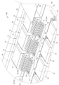
- FIG. 7 shows the main parts of the electric junction box 100 according to the second embodiment, and the case 34 and the like are omitted from the illustration.
- the basic structure of the electric junction box 100 according to the second embodiment is the same as that of the first embodiment, but in the second embodiment, the position of the terminal fitting 76c constituting the mounting portion 80 among the multiple terminal fittings 76 constituting the source terminal 28 is different.
- the same reference numerals as those in the first embodiment are used in the drawings to designate the substantially same members or parts as those in the first embodiment, and detailed description thereof will be omitted.
- the terminal fittings 76b adjacent to the control terminal 30 constitute the mounting portion 80
- the terminal fittings 76c, which are arranged in parallel with the control terminal 30, constitute the mounting portion 80. That is, in the second embodiment, the five terminal fittings 76d, which are located between the control terminal 30 and the terminal fittings 76c constituting the mounting portion 80, are mounted on the source-side bus bar 14 through the through holes 66.
- the terminal fittings 76c constituting the mounting portion 80 are connected to the conductor pattern 21 exposed on the FPC 24.
- the mounting portion 80 is formed by one of the terminal fittings 76c among the terminal fittings 76 that constitute the source terminal 28, so that the same effect as in the first embodiment can be achieved.
- the mounting portion 80 is formed by the terminal fitting 76c that is the furthest from the control terminal 30, so that each interrupter 32 is supported at three points that are spaced apart by a predetermined distance in the front-rear and left-right directions, and the risk of each interrupter 32 being tilted when mounted can be further reduced.
- each interrupter 32 is supported by the control terminal 30 and the terminal fitting 76c on both sides of the through hole 66 in the front-rear direction, each terminal fitting 76d located therebetween can be more reliably prevented from tilting so as to fall toward the source bus bar 14 side through each through hole 66.
- the terminal fitting 76c constituting the mounting portion 80 is connected to the conductor pattern 21 in the FPC 24. This makes it possible to transmit, for example, potential information obtained in each interrupter 32 to the outside via the conductor pattern 21, the control circuit in the control board 20, and the connector 70. As a result, further control is possible using the potential information obtained in each interrupter 32.
- each FPC 112 as a printed circuit board has a wide portion 114 in which the widthwise dimension (left-right dimension) of the portion overlapping with each source side connection portion 56 of the source side bus bar 14 is increased.
- the wide portion 114 of each FPC 112 overlaps not only each source side connection portion 56 but also each drain side connection portion 50 of the drain side bus bar 12 that faces each source side connection portion 56 in the left-right direction.
- the other part of the flat terminal fitting 75 is located outward in the left-right direction from the wide portion 114 of the FPC 112 and is mounted on the drain side bus bar 12, which is one of the pair of bus bars.
- the arrangement of the terminal fittings 76 on the source terminal 28 side is the same as in the first embodiment.
- the terminal fitting 76b adjacent to the control terminal 30 forms a mounting portion 80, which is placed on the substrate surface 116 of the FPC 112, and the remaining terminal fittings 76a may be mounted on the source side bus bar 14 through the through hole 66 in the FPC 112.
- two mounting sections 80, 118 are provided in each blocking section 32.
- the control terminal 30 and one terminal fitting 76b are mounted on the board surface 116 of the FPC 112, and a part of the flat terminal fitting 75 constituting the drain terminal 26 constitutes the mounting portion 118 and is mounted on the board surface 116 of the wide portion 114 of the FPC 112.
- the remaining part of the flat terminal fitting 75 is mounted on the drain side surface 16. That is, in the third embodiment, the main body 74 and the drain terminal 26 of each interrupter 32 are supported over almost the entire surface, and in addition, the control terminal 30 and one terminal fitting 76b (mounting portion 80) are also supported, so that the risk of each interrupter 32 being disposed at an angle can be reduced. Note that when the mounting portion 118 is provided on the drain terminal 26 side in this way, a relatively wide area of each interrupter 32 is supported, so the mounting portion 80 on the source terminal 28 side is not essential.
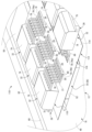
- FIG. 10 shows the main parts of the electric junction box 120 according to the fourth embodiment, and the case 34 and the like are omitted from the illustration.
- the basic structure of the fourth embodiment is similar to that of the third embodiment, for example, and each FPC 112 as a printed circuit board has a wide portion 114 in which the width dimension (left-right dimension) of the portion overlapping each source side connection portion 56 is increased.
- the wide portions 114 are formed so as not to reach the drain terminals 26. Unlike the third embodiment, the drain terminals 26 are not placed on the board surface 116 of the wide portions 114, but rather a part of the housing constituting the main body 74 is placed on the board surface 116. Thus, in the fourth embodiment, the housing portion of the main body 74 of each interrupter 32 constitutes the mounting portion 122 that is placed on the board surface 116 of each FPC 112.
- the electrical connection box 120 of the fourth embodiment which is constructed in this manner, also exhibits the same effect as the third embodiment, and the risk of each interrupter 32 being disposed at an angle can be reduced.
- the pair of power terminals in the circuit breaker are not limited in number or shape to the terminal fittings that make them up, and may be one or more, flat or straight, or may be bent in the middle in the length direction.
- the shape of the control terminal is not limited, and may extend linearly from the main body of the circuit breaker, for example.
- the drain terminal 26, the source terminal 28, and the control terminal 30 each protrude in either the left or right direction from the main body 74 of each interrupter 32, but this is not limited to this embodiment. That is, at least one of the pair of power terminals (drain terminal, source terminal) and the control terminal may protrude in the front-rear direction instead of or in addition to the left-right direction from the main body of each interrupter.
- control terminal 30 is provided outside (outside in the front-to-rear direction) each of the terminal fittings 76 that constitute the source terminal 28 in the parallel direction (front-to-rear direction) of the terminal fittings 76, but this is not limited to this aspect.
- the terminal fittings that constitute the source terminal may be disposed on both sides of the control terminal.
- the mounting portion 80 is formed by one of the terminal fittings 76b, 76c among the multiple terminal fittings 76 that constitute the source terminal 28, but this is not limited to this embodiment.
- the mounting portion may be formed by two or more of the multiple terminal fittings, and it is sufficient that the mounting portion is formed by at least one terminal fitting. Note that when the mounting portion is formed by two or more of the multiple terminal fittings, some of the multiple terminal fittings that constitute the mounting portion may be connected to the conductor pattern, or all of the multiple terminal fittings that constitute the mounting portion may be connected to the conductor pattern or may not be connected to the conductor pattern.
- the terminal fittings 76a, 76d other than the terminal fittings 76b, 76c constituting the mounting portion 80 are mounted on the source-side bus bar 14 through one through hole 66, but the number and shape of the through holes are not limited.
- multiple through holes may be formed corresponding to the multiple terminal fittings, or a circular (including elliptical, oval, etc.) through hole may be formed.
- control board 20 was provided inside the electrical connection box 10, 100, 110, 120, but it may be provided outside the electrical connection box, as long as the conductor pattern provided on the printed circuit board and the control circuit provided on the control board are electrically connected.
- the printed circuit board is an FPC (flexible printed circuit board) 24, but it may be, for example, a rigid board, and the conductor pattern on the rigid board may be electrically connected to a control circuit on a control board provided inside or outside the electrical connection box.
- FPC flexible printed circuit board
- the FPC 112 is provided with a wide portion 114 that extends all the way to the drain terminal 26.
- the drain terminal may be extended onto the printed circuit board.
- the electrical connection boxes 10, 100, 110, and 120 serving as circuit bodies were provided between the power source and the load, but this is not limited to the above. It is sufficient that the pair of bus bars are provided between two conductive paths to form a current path.
Landscapes
- Engineering & Computer Science (AREA)
- Microelectronics & Electronic Packaging (AREA)
- Power Engineering (AREA)
- Physics & Mathematics (AREA)
- Condensed Matter Physics & Semiconductors (AREA)
- General Physics & Mathematics (AREA)
- Computer Hardware Design (AREA)
- Connection Or Junction Boxes (AREA)
Abstract
Description
最初に、本開示の実施態様を列記して説明する。
本開示の回路体は、
(1)2つの導電路間の通電経路を構成する一対のバスバーと、前記一対のバスバーの表面の少なくとも一方に載置され、且つ制御回路に接続される導体パターンが基板表面に露出するプリント基板と、前記一対のバスバーの前記表面にそれぞれ実装される一対の電力端子と、前記導体パターンに実装される制御端子とを含み、前記一対のバスバー間の通電および遮断を行う遮断部と、を備え、前記一対の電力端子の少なくとも一方が、前記プリント基板の前記基板表面に載置される載置部を有している、ものである。
(8)2つの導電路間の通電経路を構成する一対のバスバーと、前記一対のバスバーの表面の少なくとも一方に載置され、且つ制御回路に接続される導体パターンが基板表面に露出するプリント基板と、前記一対のバスバーの前記表面にそれぞれ実装される一対の電力端子と、前記導体パターンに実装される制御端子とを含み、前記一対のバスバー間の通電および遮断を行う遮断部と、を備え、前記遮断部の本体部における筐体部分により、前記プリント基板の前記基板表面に載置される載置部が構成されている、ものである。
本開示の回路体の具体例を、以下に図面を参照しつつ説明する。なお、本開示は、これらの例示に限定されるものではなく、特許請求の範囲によって示され、特許請求の範囲と均等の意味および範囲内でのすべての変更が含まれることが意図される。
以下、本開示の実施形態1の電気接続箱10について、図1から図6を用いて説明する。電気接続箱10は、回路体の一例である。この電気接続箱10は、例えば電気自動車やハイブリッド自動車等の車両において、2つの導電路である高電圧バッテリと高電圧負荷との間に配置されて、これらの間の通電または遮断を行うものである。なお、電気接続箱10は任意の向きで配置することができるが、以下の説明では、上下、前後、左右の各方向は、それぞれ図1に示される上下、前後、左右の各方向のことをいう。また、複数の同一部材については、一部の部材にのみ符号を付し、他の部材については符号を省略する場合がある。
電気接続箱10は、図示しない2つの導電路の一方としての電源(例えば、高電圧バッテリ)と2つの導電路の他方としての負荷(例えば、高電圧負荷)との間の通電経路を構成して略同じ高さ位置に配索される一対のバスバー(ドレイン側バスバー12およびソース側バスバー14)を備えている。また、電気接続箱10は、一対のバスバー(ドレイン側バスバー12およびソース側バスバー14)の表面(ドレイン側表面16およびソース側表面18)の少なくとも一方に載置され、且つ制御基板20に設けられる図示しない制御回路に接続される導体パターン21(図5において二点鎖線で図示)が基板表面22に露出するプリント基板としてのフレキシブルプリント基板(以下、FPC)24を備えている。さらに、電気接続箱10は、一対のバスバー(ドレイン側バスバー12およびソース側バスバー14)の表面(ドレイン側表面16およびソース側表面18)にそれぞれ実装される一対の電力端子(ドレイン端子26およびソース端子28)と、導体パターン21に実装される制御端子30とを含み、一対のバスバー(ドレイン側バスバー12およびソース側バスバー14)間の通電および遮断を行う遮断部32と、を備えている。
一対のバスバーにおける一方としてのドレイン側バスバー12は、全体として略E字状の金属平板であり、例えば導電性能に優れる銅(銅合金を含む)やアルミニウム(アルミニウム合金を含む)等の金属により形成されている。実施形態1では、図4にも示されるように、ドレイン側バスバー12におけるE字状の開口部が前方を向くように配置されている。すなわち、ドレイン側バスバー12における後方に左右方向に延びる連結部48が設けられているとともに、連結部48における左右方向両端部および左右方向中央から、前述のドレイン端子26が接続されるドレイン側接続部50が前方に延び出している。
一対のバスバーにおける他方としてのソース側バスバー14は、全体として略U字状の金属平板であり、例えば導電性能に優れる銅(銅合金を含む)やアルミニウム(アルミニウム合金を含む)等の金属により形成されている。実施形態1では、図4にも示されるように、ソース側バスバー14におけるU字状の開口部が後方を向くように配置されている。すなわち、ソース側バスバー14における前方に左右方向に延びる連結部54が設けられているとともに、連結部54における左右方向両端部から、前述のソース端子28が接続されるソース側接続部56が後方に延び出している。
一対のバスバーの他方であるソース側バスバー14の表面(ソース側表面18)には、プリント基板としてのFPC24が載置されている。FPC24における基板表面22には導体パターン21が印刷形成されており、この導体パターン21が基板表面22に露出している。
ドレイン側バスバー12におけるドレイン側接続部50とソース側バスバー14におけるソース側接続部56には、ドレイン側バスバー12とソース側バスバー14との間の通電および遮断を行う遮断部32が接続されている。実施形態1では、遮断部32が、パワー半導体であるパワーMOSFET(Metel‐Oxide‐Semiconductor Field‐Effect Transistor)とされている。また、実施形態1では、左右方向で所定の距離を隔てて対向するドレイン側接続部50とソース側接続部56にまたがって複数の遮断部32が設けられており、これら複数の遮断部32が前後方向および左右方向で並列的に配置されている。
ケース34の具体的な形状は限定されるものではないが、実施形態1では、ケース34が全体として略矩形の箱形状を有しており、前述のように、ケース34は、アッパケース36とロアケース38を含んで構成されている。ケース34(アッパケース36およびロアケース38)は、例えば合成樹脂により形成され得る。
続いて、電気接続箱10の組立工程の具体的な一例について説明する。なお、電気接続箱10の組立工程は、以下の記載に限定されない。
次に、本開示の実施形態2の回路体としての電気接続箱100について、図7を用いて説明する。図7には、実施形態2の電気接続箱100における要部が示されており、ケース34等の図示を省略している。実施形態2の電気接続箱100における基本的な構造は実施形態1と同様であるが、実施形態2では、ソース端子28を構成する複数の各端子金具76のうち、載置部80を構成する端子金具76cの位置が異ならされている。なお、以下の説明において、実施形態1と実質的に同一の部材または部位には、図中に、実施形態1と同一の符号を付すことにより詳細な説明を省略する。
次に、本開示の実施形態3の回路体としての電気接続箱110について、図8,9を用いて説明する。図8,9には、実施形態3の電気接続箱110における要部が示されており、ケース34等の図示が省略されている。実施形態3では、プリント基板としての各FPC112が、ソース側バスバー14における各ソース側接続部56に重ね合わされる部分の幅方向寸法(左右方向寸法)が大きくされた幅広部114を有している。これにより、各FPC112における幅広部114は、各ソース側接続部56だけでなく、各ソース側接続部56に対して左右方向で対向するドレイン側バスバー12における各ドレイン側接続部50にも重ね合わせられている。
次に、本開示の実施形態4の回路体としての電気接続箱120について、図10を用いて説明する。図10には、実施形態4の電気接続箱120における要部が示されており、ケース34等の図示が省略されている。実施形態4の基本的な構造は、例えば上記実施形態3と同様であり、プリント基板としての各FPC112が、各ソース側接続部56に重ね合わされる部分の幅方向寸法(左右方向寸法)が大きくされた幅広部114を有している。
以上、本開示の具体例として、実施形態1から実施形態4について詳述したが、本開示はこの具体的な記載によって限定されない。本開示の目的を達成できる範囲での変形、改良等は本開示に含まれるものである。例えば次のような実施形態の変形例も本開示の技術的範囲に含まれる。
12 ドレイン側バスバー(一対のバスバーの一方)
14 ソース側バスバー(一対のバスバーの他方)
16 ドレイン側表面
18 ソース側表面
20 制御基板
21 導体パターン
22 基板表面
24 FPC(プリント基板)
26 ドレイン端子(一対の電力端子の一方)
28 ソース端子(一対の電力端子の他方)
30 制御端子
32 遮断部
34 ケース
36 アッパケース
38 ロアケース
40 ドレイン側端部バスバー
42 ソース側端部バスバー
44 ドレイン側外部接続部
46 ソース側外部接続部
47 貫通孔
48 連結部
50 ドレイン側接続部
52 前方開口部
54 連結部
56 ソース側接続部
58 後方開口部
60 接着シート
62 底板
64 ねじ
66 貫通孔
68 折返部
70 コネクタ
72 開口部
74 本体部
75 平板状端子金具
76 端子金具
76a,76b 端子金具(実施形態1,3)
76c,76d 端子金具(実施形態2)
78 垂直部
80 載置部
82 上底壁
84 周壁
86 バスバー支持部
88 基板支持部
90 上方開口部
92 下方開口部
100 電気接続箱(回路体、実施形態2)
110 電気接続箱(回路体、実施形態3)
112 FPC(プリント基板)
114 幅広部
116 基板表面
118 載置部
120 電気接続箱(回路体、実施形態4)
122 載置部
Claims (8)
- 2つの導電路間の通電経路を構成する一対のバスバーと、
前記一対のバスバーの表面の少なくとも一方に載置され、且つ制御回路に接続される導体パターンが基板表面に露出するプリント基板と、
前記一対のバスバーの前記表面にそれぞれ実装される一対の電力端子と、前記導体パターンに実装される制御端子とを含み、前記一対のバスバー間の通電および遮断を行う遮断部と、を備え、
前記一対の電力端子の少なくとも一方が、前記プリント基板の前記基板表面に載置される載置部を有している、回路体。 - 前記2つの導電路の一方に接続された前記一対のバスバーの一方に対して、前記一対の電力端子の一方が接続され、
前記2つの導電路の他方に接続された前記一対のバスバーの他方に対して、前記一対の電力端子の他方が接続され、
他方の前記電力端子が、複数本の端子金具を含んで構成されており、少なくとも1つの前記端子金具が前記基板表面に載置された前記載置部を構成し、それ以外の前記端子金具が前記一対のバスバーの他方に実装されている、請求項1に記載の回路体。 - 前記載置部を構成する少なくとも1つの前記端子金具が、前記導体パターンに接続されている、請求項2に記載の回路体。
- 前記載置部を構成する少なくとも1つの前記端子金具が、前記導体パターンに接続されていない、請求項2または請求項3に記載の回路体。
- 複数本の前記端子金具が、前記制御端子と並んで並列配置されており、並列方向で前記制御端子から最も離れている前記端子金具を含んで前記載置部が構成されている、請求項2から請求項4のいずれか1項に記載の回路体。
- 前記一対のバスバーの他方の前記表面に前記プリント基板が載置されており、
前記プリント基板に設けられた貫通孔を介して、前記一対のバスバーの他方の前記表面が部分的に露出しており、
前記プリント基板における前記貫通孔の周囲に、前記導体パターンに実装された前記制御端子と、前記載置部を構成する少なくとも1つの前記端子金具が載置されており、
前記貫通孔を介して露出した前記表面にそれ以外の前記端子金具が実装されている、請求項2から請求項5のいずれか1項に記載の回路体。 - 前記2つの導電路の一方に接続された前記一対のバスバーの一方に対して、前記一対の電力端子の一方が接続され、
前記2つの導電路の他方に接続された前記一対のバスバーの他方に対して、前記一対の電力端子の他方が接続され、
一方の前記電力端子が、平板状端子金具を含んで構成されており、前記平板状端子金具の一部が前記基板表面に載置された前記載置部を構成し、前記平板状端子金具のその他の一部が前記一対のバスバーの一方に実装されている、請求項1から請求項6のいずれか1項に記載の回路体。 - 2つの導電路間の通電経路を構成する一対のバスバーと、
前記一対のバスバーの表面の少なくとも一方に載置され、且つ制御回路に接続される導体パターンが基板表面に露出するプリント基板と、
前記一対のバスバーの前記表面にそれぞれ実装される一対の電力端子と、前記導体パターンに実装される制御端子とを含み、前記一対のバスバー間の通電および遮断を行う遮断部と、を備え、
前記遮断部の本体部における筐体部分により、前記プリント基板の前記基板表面に載置される載置部が構成されている、回路体。
Priority Applications (3)
| Application Number | Priority Date | Filing Date | Title |
|---|---|---|---|
| JP2024576008A JPWO2024166314A1 (ja) | 2023-02-09 | 2023-02-09 | |
| CN202380093250.1A CN120660196A (zh) | 2023-02-09 | 2023-02-09 | 电路体 |
| PCT/JP2023/004413 WO2024166314A1 (ja) | 2023-02-09 | 2023-02-09 | 回路体 |
Applications Claiming Priority (1)
| Application Number | Priority Date | Filing Date | Title |
|---|---|---|---|
| PCT/JP2023/004413 WO2024166314A1 (ja) | 2023-02-09 | 2023-02-09 | 回路体 |
Publications (1)
| Publication Number | Publication Date |
|---|---|
| WO2024166314A1 true WO2024166314A1 (ja) | 2024-08-15 |
Family
ID=92262806
Family Applications (1)
| Application Number | Title | Priority Date | Filing Date |
|---|---|---|---|
| PCT/JP2023/004413 Ceased WO2024166314A1 (ja) | 2023-02-09 | 2023-02-09 | 回路体 |
Country Status (3)
| Country | Link |
|---|---|
| JP (1) | JPWO2024166314A1 (ja) |
| CN (1) | CN120660196A (ja) |
| WO (1) | WO2024166314A1 (ja) |
Citations (2)
| Publication number | Priority date | Publication date | Assignee | Title |
|---|---|---|---|---|
| JP2020022273A (ja) * | 2018-07-31 | 2020-02-06 | 株式会社オートネットワーク技術研究所 | 電気接続箱 |
| JP2020161693A (ja) * | 2019-03-27 | 2020-10-01 | 株式会社オートネットワーク技術研究所 | 回路基板及び、回路基板を含む電気接続箱の製造方法 |
-
2023
- 2023-02-09 CN CN202380093250.1A patent/CN120660196A/zh active Pending
- 2023-02-09 JP JP2024576008A patent/JPWO2024166314A1/ja active Pending
- 2023-02-09 WO PCT/JP2023/004413 patent/WO2024166314A1/ja not_active Ceased
Patent Citations (2)
| Publication number | Priority date | Publication date | Assignee | Title |
|---|---|---|---|---|
| JP2020022273A (ja) * | 2018-07-31 | 2020-02-06 | 株式会社オートネットワーク技術研究所 | 電気接続箱 |
| JP2020161693A (ja) * | 2019-03-27 | 2020-10-01 | 株式会社オートネットワーク技術研究所 | 回路基板及び、回路基板を含む電気接続箱の製造方法 |
Also Published As
| Publication number | Publication date |
|---|---|
| CN120660196A (zh) | 2025-09-16 |
| JPWO2024166314A1 (ja) | 2024-08-15 |
Similar Documents
| Publication | Publication Date | Title |
|---|---|---|
| JP4005814B2 (ja) | 電気接続箱用配電ユニット及び電気接続箱 | |
| JP4238797B2 (ja) | 電気接続箱 | |
| US11081431B2 (en) | Circuit device | |
| CN108353501B (zh) | 电路结构体 | |
| JP2020003268A (ja) | 基板構造体 | |
| JP7218677B2 (ja) | 基板構造体 | |
| WO2024166314A1 (ja) | 回路体 | |
| JP5544767B2 (ja) | 半導体装置 | |
| JP2004135396A (ja) | 電気接続箱 | |
| JP2003087938A (ja) | 電気接続箱 | |
| CN112352473B (zh) | 电路基板 | |
| WO2024185072A1 (ja) | 回路体 | |
| JP2019200948A (ja) | 電気配線板を備えた装置 | |
| US20220022337A1 (en) | Circuit board | |
| CN112400361A (zh) | 基板构造体 | |
| WO2020080248A1 (ja) | 回路構造体及び電気接続箱 | |
| WO2020017469A1 (ja) | 回路基板 | |
| JP4822050B2 (ja) | 回路構成体及びその製造方法 | |
| WO2024201929A1 (ja) | 回路構成体 | |
| JP2006254528A (ja) | 自動車用の電気接続箱 | |
| JP2006310557A (ja) | スイッチングユニット | |
| JP2003243113A (ja) | ジョイントボックス及びコネクタ | |
| CN116868464A (zh) | 电气接线箱 | |
| JP2022134365A (ja) | 通電制御装置 | |
| JP2020188092A (ja) | 配線基板 |
Legal Events
| Date | Code | Title | Description |
|---|---|---|---|
| 121 | Ep: the epo has been informed by wipo that ep was designated in this application |
Ref document number: 23921145 Country of ref document: EP Kind code of ref document: A1 |
|
| ENP | Entry into the national phase |
Ref document number: 2024576008 Country of ref document: JP Kind code of ref document: A |
|
| WWE | Wipo information: entry into national phase |
Ref document number: 2024576008 Country of ref document: JP Ref document number: 202380093250.1 Country of ref document: CN |
|
| NENP | Non-entry into the national phase |
Ref country code: DE |
|
| WWP | Wipo information: published in national office |
Ref document number: 202380093250.1 Country of ref document: CN |