WO2022044865A1 - 半導体発光装置及び光源装置 - Google Patents
半導体発光装置及び光源装置 Download PDFInfo
- Publication number
- WO2022044865A1 WO2022044865A1 PCT/JP2021/029884 JP2021029884W WO2022044865A1 WO 2022044865 A1 WO2022044865 A1 WO 2022044865A1 JP 2021029884 W JP2021029884 W JP 2021029884W WO 2022044865 A1 WO2022044865 A1 WO 2022044865A1
- Authority
- WO
- WIPO (PCT)
- Prior art keywords
- light emitting
- semiconductor light
- emitting device
- metal layer
- wiring board
- Prior art date
- Legal status (The legal status is an assumption and is not a legal conclusion. Google has not performed a legal analysis and makes no representation as to the accuracy of the status listed.)
- Ceased
Links
Images


Classifications
-
- H—ELECTRICITY
- H01—ELECTRIC ELEMENTS
- H01S—DEVICES USING THE PROCESS OF LIGHT AMPLIFICATION BY STIMULATED EMISSION OF RADIATION [LASER] TO AMPLIFY OR GENERATE LIGHT; DEVICES USING STIMULATED EMISSION OF ELECTROMAGNETIC RADIATION IN WAVE RANGES OTHER THAN OPTICAL
- H01S5/00—Semiconductor lasers
- H01S5/02—Structural details or components not essential to laser action
- H01S5/022—Mountings; Housings
- H01S5/0225—Out-coupling of light
- H01S5/02257—Out-coupling of light using windows, e.g. specially adapted for back-reflecting light to a detector inside the housing
-
- H—ELECTRICITY
- H01—ELECTRIC ELEMENTS
- H01S—DEVICES USING THE PROCESS OF LIGHT AMPLIFICATION BY STIMULATED EMISSION OF RADIATION [LASER] TO AMPLIFY OR GENERATE LIGHT; DEVICES USING STIMULATED EMISSION OF ELECTROMAGNETIC RADIATION IN WAVE RANGES OTHER THAN OPTICAL
- H01S5/00—Semiconductor lasers
- H01S5/005—Optical components external to the laser cavity, specially adapted therefor, e.g. for homogenisation or merging of the beams or for manipulating laser pulses, e.g. pulse shaping
- H01S5/0064—Anti-reflection components, e.g. optical isolators
-
- H—ELECTRICITY
- H01—ELECTRIC ELEMENTS
- H01S—DEVICES USING THE PROCESS OF LIGHT AMPLIFICATION BY STIMULATED EMISSION OF RADIATION [LASER] TO AMPLIFY OR GENERATE LIGHT; DEVICES USING STIMULATED EMISSION OF ELECTROMAGNETIC RADIATION IN WAVE RANGES OTHER THAN OPTICAL
- H01S5/00—Semiconductor lasers
- H01S5/005—Optical components external to the laser cavity, specially adapted therefor, e.g. for homogenisation or merging of the beams or for manipulating laser pulses, e.g. pulse shaping
- H01S5/0071—Optical components external to the laser cavity, specially adapted therefor, e.g. for homogenisation or merging of the beams or for manipulating laser pulses, e.g. pulse shaping for beam steering, e.g. using a mirror outside the cavity to change the beam direction
-
- H—ELECTRICITY
- H01—ELECTRIC ELEMENTS
- H01S—DEVICES USING THE PROCESS OF LIGHT AMPLIFICATION BY STIMULATED EMISSION OF RADIATION [LASER] TO AMPLIFY OR GENERATE LIGHT; DEVICES USING STIMULATED EMISSION OF ELECTROMAGNETIC RADIATION IN WAVE RANGES OTHER THAN OPTICAL
- H01S5/00—Semiconductor lasers
- H01S5/02—Structural details or components not essential to laser action
- H01S5/022—Mountings; Housings
- H01S5/02208—Mountings; Housings characterised by the shape of the housings
-
- H—ELECTRICITY
- H01—ELECTRIC ELEMENTS
- H01S—DEVICES USING THE PROCESS OF LIGHT AMPLIFICATION BY STIMULATED EMISSION OF RADIATION [LASER] TO AMPLIFY OR GENERATE LIGHT; DEVICES USING STIMULATED EMISSION OF ELECTROMAGNETIC RADIATION IN WAVE RANGES OTHER THAN OPTICAL
- H01S5/00—Semiconductor lasers
- H01S5/02—Structural details or components not essential to laser action
- H01S5/022—Mountings; Housings
- H01S5/02218—Material of the housings; Filling of the housings
-
- H—ELECTRICITY
- H01—ELECTRIC ELEMENTS
- H01S—DEVICES USING THE PROCESS OF LIGHT AMPLIFICATION BY STIMULATED EMISSION OF RADIATION [LASER] TO AMPLIFY OR GENERATE LIGHT; DEVICES USING STIMULATED EMISSION OF ELECTROMAGNETIC RADIATION IN WAVE RANGES OTHER THAN OPTICAL
- H01S5/00—Semiconductor lasers
- H01S5/02—Structural details or components not essential to laser action
- H01S5/022—Mountings; Housings
- H01S5/023—Mount members, e.g. sub-mount members
-
- H—ELECTRICITY
- H01—ELECTRIC ELEMENTS
- H01S—DEVICES USING THE PROCESS OF LIGHT AMPLIFICATION BY STIMULATED EMISSION OF RADIATION [LASER] TO AMPLIFY OR GENERATE LIGHT; DEVICES USING STIMULATED EMISSION OF ELECTROMAGNETIC RADIATION IN WAVE RANGES OTHER THAN OPTICAL
- H01S5/00—Semiconductor lasers
- H01S5/02—Structural details or components not essential to laser action
- H01S5/022—Mountings; Housings
- H01S5/0233—Mounting configuration of laser chips
- H01S5/02345—Wire-bonding
-
- H—ELECTRICITY
- H01—ELECTRIC ELEMENTS
- H01S—DEVICES USING THE PROCESS OF LIGHT AMPLIFICATION BY STIMULATED EMISSION OF RADIATION [LASER] TO AMPLIFY OR GENERATE LIGHT; DEVICES USING STIMULATED EMISSION OF ELECTROMAGNETIC RADIATION IN WAVE RANGES OTHER THAN OPTICAL
- H01S5/00—Semiconductor lasers
- H01S5/02—Structural details or components not essential to laser action
- H01S5/024—Arrangements for thermal management
- H01S5/02461—Structure or details of the laser chip to manipulate the heat flow, e.g. passive layers in the chip with a low heat conductivity
-
- H—ELECTRICITY
- H01—ELECTRIC ELEMENTS
- H01S—DEVICES USING THE PROCESS OF LIGHT AMPLIFICATION BY STIMULATED EMISSION OF RADIATION [LASER] TO AMPLIFY OR GENERATE LIGHT; DEVICES USING STIMULATED EMISSION OF ELECTROMAGNETIC RADIATION IN WAVE RANGES OTHER THAN OPTICAL
- H01S5/00—Semiconductor lasers
- H01S5/02—Structural details or components not essential to laser action
- H01S5/024—Arrangements for thermal management
- H01S5/02469—Passive cooling, e.g. where heat is removed by the housing as a whole or by a heat pipe without any active cooling element like a TEC
-
- H—ELECTRICITY
- H01—ELECTRIC ELEMENTS
- H01S—DEVICES USING THE PROCESS OF LIGHT AMPLIFICATION BY STIMULATED EMISSION OF RADIATION [LASER] TO AMPLIFY OR GENERATE LIGHT; DEVICES USING STIMULATED EMISSION OF ELECTROMAGNETIC RADIATION IN WAVE RANGES OTHER THAN OPTICAL
- H01S5/00—Semiconductor lasers
- H01S5/02—Structural details or components not essential to laser action
- H01S5/022—Mountings; Housings
- H01S5/023—Mount members, e.g. sub-mount members
- H01S5/02315—Support members, e.g. bases or carriers
-
- H—ELECTRICITY
- H01—ELECTRIC ELEMENTS
- H01S—DEVICES USING THE PROCESS OF LIGHT AMPLIFICATION BY STIMULATED EMISSION OF RADIATION [LASER] TO AMPLIFY OR GENERATE LIGHT; DEVICES USING STIMULATED EMISSION OF ELECTROMAGNETIC RADIATION IN WAVE RANGES OTHER THAN OPTICAL
- H01S5/00—Semiconductor lasers
- H01S5/02—Structural details or components not essential to laser action
- H01S5/022—Mountings; Housings
- H01S5/0233—Mounting configuration of laser chips
- H01S5/0234—Up-side down mountings, e.g. Flip-chip, epi-side down mountings or junction down mountings
-
- H—ELECTRICITY
- H01—ELECTRIC ELEMENTS
- H01S—DEVICES USING THE PROCESS OF LIGHT AMPLIFICATION BY STIMULATED EMISSION OF RADIATION [LASER] TO AMPLIFY OR GENERATE LIGHT; DEVICES USING STIMULATED EMISSION OF ELECTROMAGNETIC RADIATION IN WAVE RANGES OTHER THAN OPTICAL
- H01S5/00—Semiconductor lasers
- H01S5/02—Structural details or components not essential to laser action
- H01S5/022—Mountings; Housings
- H01S5/0235—Method for mounting laser chips
- H01S5/02355—Fixing laser chips on mounts
- H01S5/0237—Fixing laser chips on mounts by soldering
-
- H—ELECTRICITY
- H01—ELECTRIC ELEMENTS
- H01S—DEVICES USING THE PROCESS OF LIGHT AMPLIFICATION BY STIMULATED EMISSION OF RADIATION [LASER] TO AMPLIFY OR GENERATE LIGHT; DEVICES USING STIMULATED EMISSION OF ELECTROMAGNETIC RADIATION IN WAVE RANGES OTHER THAN OPTICAL
- H01S5/00—Semiconductor lasers
- H01S5/02—Structural details or components not essential to laser action
- H01S5/022—Mountings; Housings
- H01S5/0239—Combinations of electrical or optical elements
Definitions
- This disclosure relates to a semiconductor light emitting device and a light source device.
- a semiconductor light emitting device in which a semiconductor light emitting element such as a semiconductor laser element is mounted on a substrate and the semiconductor light emitting element is covered with a cap has been proposed (see, for example, Patent Documents 1 and 2).
- Patent Documents 1 and 2 propose a structure in which a semiconductor laser element is mounted on a substrate via a submount and a cap for covering the semiconductor laser element is arranged on the substrate. A transparent plate for extracting laser light is arranged on the side surface of the cap.
- the present disclosure has been made to solve such a problem, and an object of the present invention is to provide a semiconductor light emitting device having a simplified configuration and capable of realizing high light output and reliability improvement of a semiconductor light emitting device. And.
- one aspect of the semiconductor light emitting device is a wiring board, a semiconductor light emitting element arranged on the upper surface of the wiring board, and the semiconductor light emitting device arranged on the upper surface of the wiring board.
- a cap unit for covering the element is provided, and the wiring board is arranged on the first board, a first metal layer and a second metal layer arranged apart from each other on the first board, and the first board.
- the bonding surface of the cap unit to be joined to the wiring board intersects the first metal layer and the second metal layer in the top view of the wiring board, and the spacer layer is formed by the spacer layer. It is arranged at a position different from that of the first metal layer and the second metal layer between the joint surface and the first substrate.
- the wiring board further has a first insulating layer arranged on the upper surface of the first board, and the first metal layer, the second metal layer, and the like. And the spacer layer may be arranged on the first insulating layer.
- the first substrate may be a metal substrate.
- the metal substrate may be made of a metal flat plate.
- an opening may be formed in the first insulating layer, and the semiconductor light emitting device may be arranged in the opening.
- the spacer layer may be arranged along the bonding surface.
- the wiring board may have the first metal layer, the second metal layer, and the second insulating layer covering at least a part of the spacer layer. good.
- the spacer layer may be made of a metal material.
- the spacer layer is made of the same material as the first metal layer or the second metal layer, and is the same as the first metal layer or the second metal layer. It may be electrically connected.
- the cap unit has a rectangular top plate and four side walls connected to four sides of the peripheral edge of the top plate, respectively, and the four side walls of the four side walls.
- One of them is a translucent window having an inorganic translucent plate and an antireflection film arranged on the inorganic translucent plate, and light emitted from the semiconductor light emitting device is transmitted through the translucent window. You may.
- the top plate may be transparent.
- the distance between the translucent window and the emission surface of the semiconductor light emitting device may be larger than zero and less than the thickness of the translucent window.
- the thickness of the side wall other than the translucent window among the four side walls may be larger than the thickness of the transmissive window.
- the cap unit has a rectangular top plate and four side walls connected to four sides of the peripheral edge of the top plate, and the top plate has four side walls. It is a translucent window having an inorganic translucent plate and an antireflection film formed on the inorganic translucent plate, and light emitted from the semiconductor light emitting device may pass through the translucent window.
- the semiconductor light emitting device includes a reflective optical element, and light emitted from the semiconductor light emitting element is reflected by the reflected optical element and is applied to the upper surface of the wiring substrate. It may propagate in the vertical direction.
- one aspect of the semiconductor light emitting device may include a functional element arranged on the wiring board.
- the functional element may be covered with the cap unit.
- the functional element may be a temperature detecting element.
- the temperature detecting element may be arranged at a position that does not intersect with the optical axis of the semiconductor light emitting device.
- one aspect of the semiconductor light emitting device may further include a shielding member arranged between the temperature detecting element and the semiconductor light emitting device.
- an oblique cut surface may be provided at the end of the first substrate.
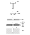
- one aspect of the light source device is a semiconductor light emitting device, a heat sink in which the semiconductor light emitting device is arranged, and a fixing screw for fixing the semiconductor light emitting device to the heat sink.
- the wiring board is formed with a through hole, and the fixing screw penetrates the through hole and is fixed to the heat sink.
- one aspect of the light source device includes a cable having terminals and a terminal fixing screw, and the wiring board has a take-out electrode electrically connected to the first metal layer.
- An electrode through hole is formed in the center of the take-out electrode, the terminal fixing screw penetrates the electrode through hole, and the terminal is arranged between the terminal fixing screw and the take-out electrode to form a take-out electrode.
- the terminal may be electrically connected.
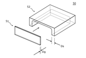
- FIG. 1A is a schematic perspective view showing the overall configuration of the semiconductor light emitting device according to the first embodiment.
- FIG. 1B is a schematic top view showing the overall configuration of the semiconductor light emitting device according to the first embodiment.
- FIG. 2 is a schematic perspective view showing the internal configuration of the cap unit of the semiconductor light emitting device according to the first embodiment.
- FIG. 3A is a schematic exploded perspective view illustrating the overall configuration of the semiconductor light emitting device according to the first embodiment.
- FIG. 3B is an equivalent circuit for explaining the circuit configuration of the semiconductor light emitting device according to the first embodiment.
- FIG. 4 is a schematic cross-sectional view illustrating the overall configuration of the semiconductor light emitting device according to the first embodiment.
- FIG. 5 is a schematic top view showing the positional relationship between the semiconductor light emitting device, each metal layer, and each spacer layer of the semiconductor light emitting device according to the first embodiment and the joint surface of the cap unit.
- FIG. 6A is a schematic cross-sectional view showing a bonding state between the wiring board according to the comparative example and the cap unit.
- FIG. 6B is a schematic cross-sectional view showing a bonding state between the wiring board according to the first embodiment and the cap unit.
- FIG. 7 is a schematic diagram illustrating each dimension of the first metal layer according to the first embodiment.
- FIG. 8 is a graph showing the relationship between the applied current of the semiconductor light emitting device according to the first embodiment, the operating voltage, and the optical output.
- FIG. 10A is a schematic cross-sectional view illustrating the first step of the method for manufacturing a wiring board according to the first embodiment.
- FIG. 10B is a schematic cross-sectional view illustrating a second step of the method for manufacturing a wiring board according to the first embodiment.
- FIG. 10C is a schematic cross-sectional view illustrating a third step of the method for manufacturing a wiring board according to the first embodiment.
- FIG. 10D is a schematic cross-sectional view illustrating a fourth step of the method for manufacturing a wiring board according to the first embodiment.
- FIG. 10E is a schematic cross-sectional view illustrating a fifth step of the method for manufacturing a wiring board according to the first embodiment.
- FIG. 10F is a schematic cross-sectional view illustrating a sixth step of the method for manufacturing a wiring board according to the first embodiment.
- FIG. 10G is a schematic cross-sectional view illustrating a seventh step of the method for manufacturing a wiring board according to the first embodiment.
- FIG. 11 is a schematic perspective view illustrating a method of manufacturing a cap unit according to the first embodiment.
- FIG. 12A is a schematic cross-sectional view illustrating a method of attaching the cap unit according to the first embodiment to the wiring board.
- FIG. 12B is a schematic cross-sectional view of a light source device using the semiconductor light emitting device according to the first embodiment.
- FIG. 13A is a schematic top view showing the configuration of each spacer layer of the semiconductor light emitting device according to the first modification of the first embodiment.
- FIG. 13B is a schematic top view showing the configuration of each spacer layer of the semiconductor light emitting device according to the second modification of the first embodiment.
- FIG. 14A is a schematic top view showing the positional relationship between the semiconductor light emitting device, the temperature detecting element, and the shielding member of the semiconductor light emitting device according to the third modification of the first embodiment.
- FIG. 14B is a schematic cross-sectional view showing the positional relationship between the semiconductor light emitting device, the temperature detecting element, and the shielding member of the semiconductor light emitting device according to the third modification of the first embodiment.
- FIG. 14A is a schematic top view showing the positional relationship between the semiconductor light emitting device, the temperature detecting element, and the shielding member of the semiconductor light emitting device according to the third modification of the first embodiment.
- FIG. 15 is a schematic perspective view showing the overall configuration of the semiconductor light emitting device according to the second embodiment.
- FIG. 16 is a schematic perspective view showing the overall configuration of the semiconductor light emitting device according to the second embodiment.
- FIG. 17 is a schematic cross-sectional view showing the overall configuration of the semiconductor light emitting device according to the second embodiment.
- FIG. 18 is a top view showing the arrangement of the temperature detecting element according to the second embodiment.
- FIG. 19A is a schematic first cross-sectional view illustrating a method of joining the cap unit of the semiconductor light emitting device according to the second embodiment to the wiring board.
- FIG. 19B is a schematic second sectional view illustrating a method of joining the cap unit of the semiconductor light emitting device according to the second embodiment to the wiring board.
- FIG. 19C is a schematic third sectional view illustrating a method of joining the cap unit of the semiconductor light emitting device according to the second embodiment to the wiring board.
- FIG. 20 is a schematic perspective view showing the configuration of the light source device according to the second embodiment.
- FIG. 21 is a schematic exploded perspective view showing the configuration of the light source device according to the second embodiment.
- FIG. 22A is a schematic cross-sectional view showing a state in which the terminal fixing screw according to the first modification of the second embodiment is fixed to the heat sink.
- FIG. 22B is an exploded cross-sectional view showing a method of fixing the terminal fixing screw to the heat sink according to the first modification of the second embodiment.
- FIG. 23 is a schematic perspective view showing the overall configuration of the semiconductor light emitting device according to the third embodiment.
- FIG. 24 is a schematic exploded perspective view showing the overall configuration of the semiconductor light emitting device according to the third embodiment.
- FIG. 25 is a schematic cross-sectional view showing the overall configuration of the semiconductor light emitting device according to the third embodiment.
- FIG. 26 is a schematic top view showing the overall configuration of the semiconductor light emitting device according to the modified example of the third embodiment.
- FIG. 27 is a schematic top view showing the overall configuration of the semiconductor light emitting device according to the fourth embodiment.
- FIG. 28 is a schematic perspective view showing the configuration of the semiconductor light emitting device according to the reference example.
- each figure is a schematic diagram and is not necessarily exactly illustrated. Therefore, the scales and the like do not always match in each figure.
- the same reference numerals are given to substantially the same configurations, and duplicate explanations will be omitted or simplified.
- the terms “upper” and “lower” do not refer to the upward direction (vertically upward) and the downward direction (vertically downward) in absolute spatial recognition, but are based on the stacking order in the laminated configuration. It is used as a term defined by the relative positional relationship. Also, the terms “upper” and “lower” are used not only when the two components are spaced apart from each other and another component exists between the two components, but also when the two components are present. It also applies when they are placed in contact with each other.
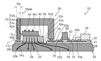
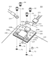
- FIGS. 1A and 1B are schematic perspective views and top views showing the overall configuration of the semiconductor light emitting device 10 according to the present embodiment, respectively.
- FIG. 2 is a schematic perspective view showing the internal configuration of the cap unit 50 of the semiconductor light emitting device 10 according to the present embodiment.
- FIG. 2 shows a semiconductor light emitting device 10 in a state where a part of the cap unit 50 is removed.
- FIG. 3A is a schematic exploded perspective view illustrating the overall configuration of the semiconductor light emitting device 10 according to the present embodiment.
- FIG. 3B is an equivalent circuit for explaining the circuit configuration of the semiconductor light emitting device 10 according to the present embodiment.
- FIG. 4 is a schematic cross-sectional view illustrating the overall configuration of the semiconductor light emitting device 10 according to the present embodiment.
- FIG. 4 shows a semiconductor light emitting device 10 in a cross section along the IV-IV line shown in FIG. 1B.
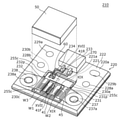
- the semiconductor light emitting device 10 is a device that emits light, and includes a wiring substrate 20, a semiconductor light emitting element 41, and a cap unit 50, as shown in FIG. 3A.
- the semiconductor light emitting device 10 further includes a submount 45, a temperature detecting element 60, a connector 70, and joining members 26, 42, 55, and 62, as shown in FIG.
- each component of the semiconductor light emitting device 10 will be described.
- the wiring board 20 is a plate-shaped member that serves as a base for the semiconductor light emitting device 10 and is provided with wiring.
- the upper surface 20a of the wiring board 20 is a component mounting surface, and the lower surface facing the upper surface 20a (that is, the surface on the back side of the upper surface 20a) is the heat dissipation surface 20b.
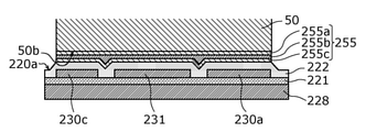
- the wiring board 20 includes a metal substrate 28, a first insulating layer 21, a second insulating layer 22, spacer layers 30a and 30b, a third metal layer 33, and a fourth metal layer. It has 34 and protective films 25 and 35. Further, as shown in FIGS.
- the wiring board 20 further includes a first metal layer 31, a second metal layer 32, a first pad electrode 31p, and a second pad electrode 32p.
- the first metal layer 31, the second metal layer 32, the third metal layer 33, the fourth metal layer 34, and each spacer layer are the second insulating layer. Since it is covered with 22, it does not appear on the surface. However, since the portion of the second insulating layer 22 on each layer projects upward, the position of the edge of each layer is shown as the position of the step of the second insulating layer 22. Further, since each of the above layers is covered with the second insulating layer 22, a broken line leader line is attached to the reference numeral indicating these metal layers. The same applies to each metal layer and each spacer layer shown in the top view and the perspective view described below.
- the wiring board 20 is formed with through holes 28a and 28b and positioning holes 29a and 29b.
- the through holes 28a and 28b are holes for inserting a fixing member such as a screw when fixing the wiring board 20 in close contact with a heat sink or the like.
- the through holes 28a and 28b are arranged on one side and the other side on the opposite side of the region where the semiconductor light emitting element 41 of the wiring board 20 is arranged, respectively.
- the upward direction and the downward direction of FIG. 1B will be referred to as one and the other, respectively.
- the semiconductor light emitting device 41 is arranged between the through hole 28a and the through hole 28b.
- the positioning holes 29a and 29b are holes for positioning with respect to the heat sink or the like when the wiring board 20 is fixed to the heat sink or the like.
- positioning pins provided at positions such as heat sinks where positioning holes 29a and 29b should be arranged are fitted into the positioning holes 29a and 29b, respectively.
- the wiring board 20 can be positioned at a predetermined position such as a heat sink.
- the positioning hole 29a is a first positioning hole, and is a hole having a circular shape in the top view of the wiring board 20.
- the positioning hole 29b is a second positioning hole, and is a hole having an elongated hole shape (that is, an oval shape) in the top view of the wiring board 20.
- the metal substrate 28 is an example of the first substrate of the wiring board 20.
- the metal substrate 28 is composed of a flat plate of a metal such as oxygen-free copper or a copper alloy.
- the flat plate is a plate having a depth or height larger than the surface roughness and having no patterned uneven shape formed on the surface of a surface other than the peripheral portion.
- a flat first insulating layer 21 can be formed on the metal substrate 28. This facilitates the formation of a thick metal layer on the first insulating layer 21.
- the metal substrate 28 is, for example, a flat plate made of oxygen-free copper having a thickness of 0.5 mm or more and 3 mm or less.
- the shape of the metal substrate 28 (that is, the shape in the top view) is, for example, a rectangle, and the length of one side of the metal substrate 28 is, for example, about 5 mm or more and 30 mm or less.
- an oblique cut surface 28c which is an inclined surface inclined with respect to the main surface of the metal substrate 28, is formed on the edge portion of the metal substrate 28.
- the first insulating layer 21 is formed on the upper surface of the metal substrate 28, and the insulating layer is not formed on the lower surface of the metal substrate 28 (that is, the surface on the back side of the upper surface).
- the entire area of the lower surface of the metal substrate 28 can be used as the heat dissipation surface 20b of the wiring board 20, so that heat can be dissipated in a large area. Therefore, it is possible to use a high light output semiconductor light emitting device 41 having a large calorific value.
- the first insulating layer 21 is an insulating layer arranged on the upper surface of the metal substrate 28.
- the first insulating layer 21 is made of an insulating material such as epoxy glass or ceramic having a thickness of 0.05 mm or more and 0.3 mm or less, for example.
- an opening 21a is formed in the first insulating layer 21.
- a part of the first insulating layer 21 is removed to form a rectangular opening 21a.
- the opening 21a is formed at a position closer to the edge than the central portion in the top view of the metal substrate 28.
- a protective film 25 made of Ni, Au, etc. is formed in the region of the metal substrate 28 corresponding to the opening 21a, and a mounting surface for mounting the semiconductor light emitting element 41 is formed. ..
- the semiconductor light emitting element 41 is arranged in the opening 21a via the submount 45.
- the first metal layer 31, the second metal layer 32, the third metal layer 33, and the fourth metal layer 34 are metal layers arranged apart from each other on the first substrate, and in the present embodiment, the first metal layer 31 and the fourth metal layer 34 are arranged apart from each other. 1 Arranged on the insulating layer 21.
- the first metal layer 31 and the second metal layer 32 are wirings for supplying power to the semiconductor light emitting device 41.
- the third metal layer 33 and the fourth metal layer 34 are wirings connected to the temperature detecting element 60.
- Each metal layer forms a convex portion on the first insulating layer 21.
- the first metal layer 31, the second metal layer 32, the third metal layer 33, and the fourth metal layer 34 are, for example, metal layers composed of copper having a thickness of 0.02 mm or more and 0.15 mm or less. ..
- the spacer layers 30a and 30b are layers arranged at positions different from those of the first metal layer 31 and the second metal layer 32 on the first substrate, and are arranged on the first insulating layer 21 in the present embodiment. .. As shown in FIG. 4, the spacer layers 30a and 30b are arranged between the joint surface 50b of the cap unit 50 with the wiring board 20 and the first insulating layer 21. The spacer layers 30a and 30b form convex portions on the first insulating layer 21 in the same manner as the metal layers.
- the materials constituting the spacer layers 30a and 30b are not particularly limited. In this embodiment, the spacer layers 30a and 30b are made of a metal material.
- the spacer layers 30a and 30b are, for example, metal layers made of copper having a thickness of 0.02 mm or more and 0.15 mm or less, similar to the first metal layer 31 and the like.
- the second insulating layer 22 is an insulating layer arranged on the first insulating layer 21.
- the second insulating layer 22 has a function of covering at least a part of the first metal layer 31, the second metal layer 32, the third metal layer 33, the fourth metal layer 34, the spacer layers 30a and 30b, and protecting each of these layers. Also has.
- the second insulating layer 22 is, for example, an insulating layer made of a resin such as polyimide or epoxy having a thickness of 0.05 mm or more and 0.2 mm or less.
- the protective film 25 is a metal film arranged at a position or the like where the submount 45 or the like is joined on the wiring board 20.
- the protective film 25 is arranged in the region corresponding to the opening 21a of the first insulating layer 21 of the metal substrate 28.
- the protective film 35 is a metal film in which a metal layer such as the first metal layer 31 is arranged on a surface exposed from the second insulating layer 22.
- the protective film 35 is arranged on a part of the upper surface of the first metal layer 31, the second metal layer 32, the third metal layer 33, and the fourth metal layer 34.
- the protective films 25 and 35 also have a role of a rust preventive film that protects exposed surfaces such as the metal substrate 28 and the first metal layer 31 from oxidation and the like.
- the protective films 25 and 35 are made of, for example, Ni, Au and the like.
- the first pad electrode 31p and the second pad electrode 32p are pad-shaped electrodes arranged on the portions of the first metal layer 31 and the second metal layer 32 adjacent to the semiconductor light emitting device 41, respectively. As shown in FIGS. 2 and 3A, the metal wires W2 and W3 are bonded to the first pad electrode 31p and the second pad electrode 32p, respectively.
- the first pad electrode 31p and the second pad electrode 32p are also a part of the protective film 35, and are composed of, for example, Ni, Au, and the like.
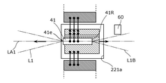
- the semiconductor light emitting element 41 is a light emitting element arranged on the upper surface 20a of the wiring board 20.
- the semiconductor light emitting device 41 is arranged in the opening 21a of the first insulating layer 21.
- the semiconductor light emitting device 41 is, for example, a light emitting device made of a compound semiconductor such as gallium nitride based or gallium arsenide based.
- the semiconductor light emitting device 41 is a semiconductor laser device having an optical waveguide extending in a direction parallel to the main surface of the metal substrate 28.
- the semiconductor light emitting device 41 is mounted on the submount 45.
- the semiconductor light emitting device 41 has a substrate and a semiconductor laminate laminated on the substrate.
- An optical waveguide is formed on the semiconductor laminate.
- the semiconductor laminate of the semiconductor light emitting device 41 is arranged so as to face the submount 45. That is, the semiconductor light emitting device 41 is junction-down mounted on the submount 45. Electrodes (not shown) are provided on the upper surface (that is, the upper surface of the semiconductor light emitting device 41 in FIG. 4) and the lower surface (that is, the lower surface of the semiconductor light emitting device 41 in FIG. 4) of the semiconductor light emitting device 41, respectively. It is formed.
- the lower surface of the semiconductor light emitting device 41 faces the upper surface of the submount 45.
- the electrode formed on the lower surface of the semiconductor light emitting device 41 facing the submount 45 is electrically connected to the first electrode 47 formed on the upper surface of the submount 45. More specifically, the electrode formed on the lower surface of the semiconductor light emitting device 41 is electrically connected to the first electrode 47 formed on the upper surface of the submount 45 via a joining member 42 (see FIG. 4) made of AuSn solder or the like. Be connected.
- the electrode formed on the upper surface of the semiconductor light emitting device 41 is electrically connected to the second electrode 48 formed on the upper surface of the submount 45 via the metal wire W1.
- the first electrode 47 and the second electrode 48 formed on the upper surface of the submount 45 are electrically connected to the first pad electrode 31p and the second pad electrode 32p, respectively, via the metal wires W2 and W3.
- the current can be supplied to the semiconductor light emitting device 41 by using the first metal layer 31 and the second metal layer 32 connected to the first pad electrode 31p and the second pad electrode 32p, respectively.
- the semiconductor light emitting device 41 has a light emitting point 41e that emits the emitted light L1.
- the emitted light L1 is a laser beam.
- the emitted light L1 is laser light having a peak wavelength in the range of, for example, a wavelength of 270 nm or more and 600 nm or less when the semiconductor light emitting device 41 contains a gallium nitride compound semiconductor, and the semiconductor light emitting device 41 is a gallium phosphate indium type.
- a compound semiconductor or a gallium arsenide compound semiconductor is included, it is, for example, a laser beam having a peak wavelength in the range of 600 nm or more and 10.4 ⁇ m or less.
- the light emitting point 41e is an end portion of the optical waveguide of the semiconductor light emitting device 41 located on the left side of FIG.
- the semiconductor light emitting device 41 is arranged so that the emission surface, which is the end surface on which the light emitting point 41e is arranged, protrudes from the end surface of the submount 45 (the left end surface of the submount 45 shown in FIG. 4). As a result, it is possible to prevent the emitted light L1 emitted from the light emitting point 41e from being blocked by the submount 45.
- the semiconductor light emitting device 41 has, for example, a rectangular parallelepiped shape having a width of 0.2 mm or more and 2 mm or less, a length of 1 mm or more and 9 mm or less, and a thickness of 0.08 mm or more and 0.2 mm or less. ..
- the submount 45 is a member arranged between the wiring board 20 and the semiconductor light emitting element 41.
- the submount 45 is mounted on the upper surface 20a of the wiring board 20. More specifically, as shown in FIG. 4, the submount 45 is arranged inside the opening 21a of the first insulating layer 21 and mounted on the metal substrate 28 via the joining member 26 and the protective film 25. ..
- the joining member 26 is made of, for example, AuSn solder or the like.
- a semiconductor light emitting device 41 is mounted on the upper surface of the submount 45.
- the submount 45 includes an insulating block which is a rectangular parallelepiped block made of an insulating material, a first electrode 47 and a second electrode 48 which are metal films arranged on the upper surface of the insulating block, and the like. It has a metal film (not shown) arranged on the lower surface of the insulating block.
- the insulating block is made of an insulating material having high thermal conductivity such as AlN, SiC, and diamond.
- the insulating block has, for example, a rectangular parallelepiped shape having a width of 1 mm or more and 5 mm or less, a length of 2 mm or more and 10 mm or less, and a thickness of 0.2 mm or more and 4 mm or less.
- the first electrode 47 and the second electrode 48 are arranged apart from each other and are electrically insulated. Further, the first electrode 47 and the second electrode 48 are electrically insulated from the metal film arranged on the lower surface of the insulating block.
- the metal film arranged on the lower surface of the first electrode 47, the second electrode 48, and the insulating block is a metal film made of Ni, Cu, Ti, Pt, Au, or the like.
- the semiconductor light emitting element 41 is mounted on the metal substrate 28 via the submount 45 as described above. With such a configuration, as shown by the arrow in FIG. 4, the heat generated by the semiconductor light emitting device 41 can be efficiently dissipated to the metal substrate 28 via the submount 45.
- the lower surface of the metal substrate 28 is in close contact with, for example, a heat sink (not shown).
- the heat generated by the semiconductor light emitting device 41 can be efficiently conducted from the metal substrate 28 to the heat sink.
- the metal substrate 28 according to the present embodiment is a flat plate, it is easy to manufacture and the cost can be reduced. Therefore, it is possible to realize the semiconductor light emitting device 10 which has a simplified configuration and can be manufactured at low cost.
- the cap unit 50 is a cover member arranged on the upper surface 20a of the wiring board 20 and covering the semiconductor light emitting element 41. As shown in FIG. 4, the cap unit 50 has a joint surface 50b facing the wiring board 20.
- the joining surface 50b has an annular shape, and the joining surface 50b and the upper surface 20a of the wiring board 20 are joined by a joining member 55 made of an epoxy adhesive, a silicon adhesive, AuSn solder, or the like. As a result, the space between the cap unit 50 and the wiring board 20 can be sealed.
- a joining member 55 made of an epoxy adhesive, a silicon adhesive, AuSn solder, or the like.
- the cap unit 50 includes an opening 21a of the first insulating layer 21, a semiconductor light emitting element 41 and a submount 45 arranged in the opening 21a, and a first pad. It covers the electrode 31p and the second pad electrode 32p, and a part of each of the first metal layer 31 and the second metal layer 32.
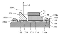
- the cap unit 50 has a rectangular top plate 52d (see FIG. 4) and four side walls 51, 52a, 52b, and 52c (see FIG. 2) connected to the four sides of the peripheral edge of the top plate 52d, respectively. Have.
- one of the four side walls 51, 52a, 52b, and 52c is a translucent window, and as shown in FIG. 4, the inorganic translucent plate 51a and the inorganic translucent translucent plate 51a.
- the side wall 51 has antireflection films 51b and 51c arranged on the plate 51a.
- the side wall 51 has antireflection films 51b and 51c arranged on each main surface of the inorganic translucent plate 51a.
- the antireflection film 51b is arranged on the main surface of the inorganic light transmitting plate 51a facing the semiconductor light emitting device 41, and the antireflection film 51c is arranged on the main surface on the back side of the main surface.
- the three side walls 52a, 52b, and 52c and the top plate 52d are integrally formed to form the holder 52.
- the side wall 51 is arranged at a position facing the light emitting point 41e of the semiconductor light emitting element 41. As a result, the light L1 emitted from the semiconductor light emitting device 41 passes through the side wall 51 which is a translucent window.
- the holder 52 is made of glass, for example.
- the holder 52 is manufactured, for example, by forming a recess in a rectangular parallelepiped glass block with a sandblaster or the like and dividing the holder 52.
- the side wall 51 and the holder 52 which are translucent windows, are joined by optical contact or laser welding to form a box-shaped cap unit.
- the cap unit 50 has the above configuration, the emitted light L1 from the semiconductor light emitting element can be easily taken out from the side wall 51 of the cap unit 50.
- the thickness Dg of the side wall 51 which is the translucent window shown in FIG. 4, is about 0.01 mm or more and 0.2 mm or less. Further, the distance Dgap between the side wall 51 which is a translucent window and the exit surface of the semiconductor light emitting element 41 (that is, the end surface including the light emitting point 41e) is larger than zero and less than the thickness Dg of the side wall 51. As a result, the distance (Dg + Dgap) from the light emitting point 41e of the semiconductor light emitting element 41 to the outside of the cap unit 50 can be reduced. Therefore, it is possible to reduce the beam cross-sectional area SL1 of the emitted light L1 on the outer surface of the cap unit 50.
- the size of the optical element can be reduced by reducing the beam cross-sectional area SL1 of the emitted light L1 , and the optical element can be reduced.
- the emitted light L1 can be easily coupled to the lens.
- the thickness of the side walls 52a, 52b, and 52c is larger than the thickness of the side wall 51, which is a translucent window. This makes it possible to increase the structural strength of the holder and the cap unit 50 while reducing the distance (Dg + Dgap) from the light emitting point 41e of the semiconductor light emitting element 41 to the outside of the cap unit 50.
- the semiconductor light emitting device 10 may include a functional element other than the semiconductor light emitting element 41.
- the semiconductor light emitting device 10 includes a temperature detecting element 60 as an example of a functional element.
- the temperature detection element 60 which is an example of the functional element, will be described.
- the temperature detecting element 60 is a temperature sensor arranged on the wiring board 20. As shown in FIG. 4, the temperature detecting element 60 is electrically connected to the third metal layer 33 and the fourth metal layer 34 via the joining member 62 and the protective film 35.
- the protective film 35 is also a pad electrode arranged on the third metal layer 33 and the fourth metal layer 34.
- the temperature detection element 60 is mounted on the surface of the wiring board 20 by a joining member 62 such as SnAgCu cream solder.
- the temperature of the wiring board 20 can be detected by the temperature detecting element 60.
- the temperature of the semiconductor light emitting element 41 mounted on the wiring board 20 via the submount 45 can be estimated. Therefore, the temperature of the semiconductor light emitting element 41 can be estimated by the temperature detecting element 60 and used for controlling the semiconductor light emitting element 41. For example, when the temperature detecting element 60 detects that the temperature of the semiconductor light emitting element 41 is higher than a predetermined threshold value, the current supplied to the semiconductor light emitting element 41 can be reduced or stopped.
- a thermistor can be used as the temperature detecting element 60.
- a predetermined voltage is applied to the temperature detecting element 60, and the current flowing through the temperature detecting element 60 is detected to detect the resistance value of the temperature detecting element 60.
- the temperature of the wiring board 20 can be detected from the correlation between the resistance value and the temperature.
- a voltage is applied to the temperature detecting element 60 via the third metal layer 33 and the fourth metal layer 34.
- the temperature detecting element 60 is arranged outside the cap unit 50. As a result, the cap unit 50 can be miniaturized. Therefore, the space between the cap unit 50 and the wiring board 20 can be easily sealed.
- the connector 70 is a connecting component having terminals connected to each of the first metal layer 31 and the second metal layer 32.
- the connector 70 connects the wiring board 20 and an external electric circuit (not shown).
- the connector 70 is a receptacle further having terminals connected to each of the third metal layer 33 and the fourth metal layer 34, as shown in FIG. 3B and the like.
- a protective film 35 is formed at the ends of the first metal layer 31, the second metal layer 32, the third metal layer 33, and the fourth metal layer 34 on the side farther from the place where the semiconductor light emitting element 41 is arranged.
- the pad electrodes 31q, 32q, 33q, and 34q are formed and connected to the connector 70.
- the connector 70 is mounted on the surface of the wiring board 20 by a joining member (not shown) such as SnAgCu cream solder, and is connected to the pad electrodes 31q, 32q, 33q, and 34q.
- FIG. 5 is a schematic top view showing the positional relationship between the semiconductor light emitting element 41, each metal layer, and each spacer layer of the semiconductor light emitting device 10 according to the present embodiment and the joint surface 50b of the cap unit 50. ..
- FIG. 5 shows the configuration of the semiconductor light emitting device 41 of the semiconductor light emitting device 10 in a state where the cap unit 50 and the second insulating layer 22 are removed, and the periphery thereof. Further, in FIG. 5, the position of the end edge of the joint surface 50b of the cap unit 50 is shown by a broken line.
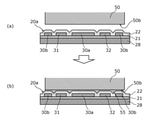
- FIG. 6A and 6B are schematic cross-sectional views showing a bonding state between each wiring board according to a comparative example and the present embodiment and a cap unit 50, respectively.
- FIG. 6B shows a wiring board 20 and the like in the cross section of the VI-VI line of FIG.
- FIG. 6A shows a cross section of the wiring board and the cap unit 50 of the comparative example at the same positions as in FIG. 6B.
- 6A and 6B are cross-sectional views (a) before joining the cap unit 50 and each wiring board, and each cross-sectional view (b) shows a cross-sectional view after joining.
- the first pad electrode 31p, the second pad electrode 32p, the first metal layer 31, and the second metal layer 32 extend in the optical axis direction of the semiconductor light emitting device 41 (that is, the optical waveguide extends. It extends in the direction, in other words, in the resonance direction).
- the first pad electrode 31p and the first metal layer 31 are arranged on one side of the semiconductor light emitting device 41 (and the opening 21a).
- the second pad electrode 32p and the second metal layer 32 are arranged on the side of the other side (direction opposite to one side) of the semiconductor light emitting element 41.
- the first metal layer 31 and the second metal layer 32 extend from the inside of the cap unit 50 toward the rear of the semiconductor light emitting device 41 (that is, in the direction opposite to the propagation direction of the emitted light L1) to the outside of the cap unit 50. Stretch. Therefore, the joint surface 50b joined to the wiring board 20 of the cap unit 50 intersects the first metal layer 31 and the second metal layer 32 in the top view of the wiring board 20.
- the portion of the first metal layer 31 where the first pad electrode 31p and the pad electrode 31q are not provided is covered with the second insulating layer 22.
- the portion of the second metal layer 32 to which the second pad electrode 32p and the pad electrode 32q are not provided is covered with the second insulating layer 22.
- the spacer layers 30a and 30b are arranged between the joint surface 50b and the first insulating layer 21.
- the spacer layer 30a is lateral to the other side of the first metal layer 31 (the side closer to the second metal layer 32) on the side of the rear end surface 41R opposite to the emission surface 41F including the light emitting point 41e of the semiconductor light emitting element 41. Therefore, it is arranged so as to extend to one side of the second metal layer 32 (the side closer to the first metal layer 31).
- the spacer layer 30b is composed of five parts.
- the first portion of the spacer layer 30b is laterally (on the main surface of the wiring board 20) from the side of one of the first metal layers 31 (the side far from the second metal layer 32) on the side of the rear end surface 41R. In the plane, it is arranged so as to extend in the direction perpendicular to the optical axis direction).
- the second portion of the spacer layer 30b is connected to the first portion, and the optical axis is on the side of one of the first pad electrode 31p and the first metal layer 31 (the side far from the second metal layer 32). Arranged to extend in the direction.
- the third portion of the spacer layer 30b is connected to the second portion and is arranged so as to extend laterally on the side of the exit surface 41F.
- the fourth portion of the spacer layer 30b is connected to the third portion, and the optical axis is on the side of the second pad electrode 32p and the other side of the second metal layer 32 (the side far from the first metal layer 31). Arranged to extend in the direction.
- the fifth portion of the spacer layer 30b is connected to the fourth portion, and on the side of the rear end surface 41R, from the side of the other side of the second metal layer 32 (the side far from the first metal layer 31). Arranged so as to extend laterally.
- the wiring board of the comparative example shown in FIG. 6A is a wiring board in which the spacer layers 30a and 30b are removed from the wiring board 20 according to the present embodiment.
- the first metal layer 31 and the second metal layer 32 according to the comparative example and the present embodiment have a large cross-sectional area so that a large current can be supplied to the semiconductor light emitting device 41. Therefore, the thickness of the first metal layer 31 and the second metal layer 32 is about 0.02 mm or more and 0.15 mm or less.
- the second insulating layer 22 on each such metal layer is formed by applying a liquid insulating material on the first metal layer 31 and the second metal layer 32 and curing the second metal layer 32, and the thickness is 0. It is about 02 mm or more and 0.1 mm or less.
- the shape of the upper surface of the second insulating layer 22 is an uneven shape along the upper surface of the first insulating layer 21 and each metal layer, as shown in the cross-sectional view (a) of FIG. 6A. That is, on the upper surface of the wiring board, a recess having a depth similar to the thickness of the first metal layer 31 and the second metal layer 32 is formed in the region between the first metal layer 31 and the second metal layer 32. Will be done.
- the joining member layer is crushed, the unnecessary joining member may protrude from the joint surface between the wiring board and the cap unit and spread on the wiring board toward the opening 21a and the connector 70. Therefore, the functions of the functional parts arranged inside and outside the cap unit are changed.
- the hole shape may change.
- the bonding member spreads from the bonding surface facing the light emitting point 41e toward the semiconductor light emitting device 41 the characteristics of the emitted light L1 may change significantly. In order to reduce the influence of the protruding joint member, it is difficult to reduce the size of the semiconductor light emitting device when the distance between the joint surface and the functional component is widened.
- the wiring board 20 and the cap unit 50 are to be bonded with a small amount of joining members, as shown in the cross-sectional view (b) of FIG. 6A, the upper surface of the wiring board and the joining surface 50b of the cap unit 50 A gap 55v in which the joining member 55 does not exist is formed between the two. Therefore, when the wiring board of the comparative example is used, it is not possible to seal between the upper surface of the wiring board and the joint surface 50b of the cap unit 50.
- the first metal layer 31 and the first metal layer 31 are between the joint surface 50b and the first insulating layer 21.
- the spacer layers 30a and 30b are arranged at positions different from those of the second metal layer 32. Since such spacer layers 30a and 30b are arranged between the first metal layer 31 and the second metal layer 32, the first metal layer 31 and the second metal layer 32 on the upper surface 20a of the wiring board 20 The dimensions and depth of the recesses formed between them in the direction parallel to the main surface of the metal substrate 28 can be reduced. Therefore, as shown in the cross-sectional view (b) of FIG.
- the recess of the upper surface 20a of the wiring board 20 can be filled with a small amount of the joining member 55. Therefore, the upper surface 20a of the wiring board 20 and the joining surface 50b of the cap unit 50 can be sealed with a small amount of joining members. Therefore, it is possible to prevent foreign matter and the like from entering the cap unit 50 and to prevent the joint member from affecting the functional parts around the joint surface. That is, a highly reliable semiconductor light emitting device 10 can be realized. Further, since the first metal layer 31 and the second metal layer 32 having a large cross-sectional area are used, a large current can be applied to the semiconductor light emitting device 10 to realize high light output.
- the spacer layers 30a and 30b are a portion of the joint surface 50b facing the first metal layer 31 and a portion facing the second metal layer 32. It is placed along the part between. As a result, it is possible to increase the portion where either the metal layer or the spacer layer is arranged between the joint surface 50b and the wiring board 20. Therefore, it is possible to reduce the formation of a gap between the joint surface 50b and the wiring board 20.
- the spacer layer 30a has a linear shape when viewed from above the wiring board 20, and is located between the portion on the first metal layer 31 and the portion on the second metal layer 32 in the joint surface 50b. Arranged along a straight line.
- the spacer layer 30b has a C-shaped shape when viewed from above the wiring board 20, and is C between the portion on the first metal layer 31 and the portion on the second metal layer 32 in the joint surface 50b. It is arranged along the character-shaped part. As a result, most of the space between the joint surface 50b and the metal substrate 28 where the first metal layer 31 and the second metal layer 32 are not arranged can be filled with the spacer layers 30a and 30b. Therefore, it is possible to further reduce the formation of a gap between the joint surface 50b and the wiring board 20.
- the thicknesses of the spacer layers 30a and 30b are equal to the thicknesses of the first metal layer 31 and the second metal layer 32. Further, the first metal layer 31, the second metal layer 32, the spacer layers 30a and 30b are covered with the second insulating layer 22 having the same thickness. As a result, the upper surface 20a of the wiring board 20 can be made even flatter, so that the formation of a gap between the joint surface 50b and the wiring board 20 can be further reduced. Further, by covering each metal layer and each spacer layer with the second insulating layer 22, it is possible to reduce the disconnection of each metal layer due to the contact of an object from the outside.
- the distance (that is, the gap) between each of the spacer layers 30a and 30b and the first metal layer 31 is the width of the first metal layer 31 (that is, the stretching direction and the thickness direction of the first metal layer 31). It is smaller than the vertical dimension). Further, the distance between each of the spacer layers 30a and 30b and the second metal layer 32 is smaller than the width of the second metal layer 32. As a result, the size of the recess formed on the upper surface 20a of the wiring board 20 can be further reduced. Further, the distance between each of the first metal layer 31 and the second metal layer 32 and the spacer layer 30a may be smaller than the width of the spacer layer 30a.
- the distance between each of the first metal layer 31 and the second metal layer 32 and the spacer layer 30b may be smaller than the width of the spacer layer 30b.
- the size of the recess formed on the upper surface 20a of the wiring board 20 can be further reduced. Therefore, it is possible to further reduce the formation of a gap between the joint surface 50b and the wiring board 20.
- the distance between each of the spacer layers 30a and 30b and the first metal layer 31 may be larger than the thickness of the first metal layer 31.
- the distance between each of the spacer layers 30a and 30b and the second metal layer 32 may be larger than the thickness of the second metal layer 32.
- FIG. 7 is a schematic diagram illustrating each dimension of the first metal layer 31 according to the present embodiment.
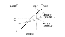
- FIG. 8 is a graph showing the relationship between the applied current of the semiconductor light emitting device 10 according to the present embodiment, the operating voltage, and the optical output.
- FIG. 9 is a table showing a design example of the metal layer.
- FIG. 7 shows a schematic diagram of the first metal layer 31 as an example of each metal layer. As shown in FIG. 7, the width of the cross section perpendicular to the stretching direction of the metal layer is W, the thickness is T, and the length in the stretching direction is L. In addition, FIG. 7 also shows the first insulating layer 21 in which the first metal layer 31 is arranged. The dimensions of the metal layers other than the first metal layer 31 are also defined in the same manner as the first metal layer 31.
- the electrical wiring composed of a metal layer has a slight (electrical) resistance.
- a current of 1 ampere or more and 50 amperes or less and a voltage of 2 volts or more and 6 volts or less are applied to the semiconductor light emitting device 41 having a high optical output of 1 watt or more and 100 watts or less.
- the voltage drop in the electrical wiring is 0.2 V even if the wiring resistance is 0.1 ⁇ . That is, the operating voltage increases by 0.2V. Therefore, the wiring resistance cannot be ignored as a factor for increasing the operating voltage of the semiconductor light emitting device 10.
- the Wall-Plug-Efficiency which is the input power-optical conversion efficiency of the semiconductor light emitting device 10
- the Wall-Plug-Efficiency is when the resistance of the electric wiring is high with respect to the value Po / (Va ⁇ If) when the resistance of the electric wiring is low. Decreases with Po / (Vb ⁇ If).
- the effect of this decrease in conversion efficiency on power consumption becomes remarkable.
- a metal layer is formed using a conductive paste containing tungsten as a main component, which is a material suitable for integral sintering. ing.
- tungsten the volume resistivity of tungsten is relatively large, about 5.7 ⁇ 10-8 ⁇ ⁇ m, and tends to be a factor of increasing wiring resistance.
- the metal layer is composed of copper having a volume resistivity of about 1.8 ⁇ 10-8 ⁇ ⁇ m, which is relatively small, or a material containing copper as a main component.
- the metal layer is formed inside the ceramic, it is necessary to improve the adhesion between the metal layer and the ceramic. Therefore, it is necessary to make the thickness T of the metal layer smaller than, for example, 50 ⁇ m. Further, the thickness T of the metal layer may be made smaller than, for example, 20 ⁇ m. As a result, it is possible to reduce the occurrence of irregularities on the surface of the ceramic layer. In such a case, the design conditions of the metal layer for reducing the wiring resistance are limited. For example, when tungsten is used as the material of the metal layer, as shown in FIG. 9, in Design Example 1, since the thickness T and the width W of the metal layer are small, the wiring resistance becomes large. Therefore, the operating voltage increases by 0.228V due to the wiring resistance. Therefore, when the applied current amount is large, it is necessary to increase the thickness T and the width W as in Design Example 2.
- the dimensions of the metal layer are set to the same level as Design Example 2 of the prior art, and the material is changed from tungsten in Design Example 2 to copper.
- the wiring resistance can be reduced to about 1/3 as compared with the design example 2. Therefore, the voltage increase due to the wiring resistance can be reduced to 1% or less of the operating voltage.
- the thickness T of the metal layers constituting the first metal layer 31 and the second metal layer 32 may be 0.05 mm or more. Thereby, the resistance in the first metal layer 31 and the second metal layer 32 can be reduced. Therefore, a convex portion having a height of 0.05 mm or more is formed on the upper surface 20a of the wiring board 20. Further, even when the metal layer and the first insulating layer 21 are covered with a resin such as a resist as the second insulating layer 22, the thickness of the second insulating layer 22 is 0.02 mm or more and 0.1 mm. Since it is about the following, it is difficult to flatten the upper surface 20a of the wiring board 20. Further, the width of each metal layer may be 1 mm or more.
- the wiring resistance of each metal layer can be reduced. Further, in order to reduce the wiring resistance, it is necessary to make the length of each metal layer as short as possible. Therefore, the first metal layer 31 and the second metal layer 32 are connected between the first pad electrode 31p and the second pad electrode 32p and the connector 70 at the shortest distance, for example, in a straight line. Therefore, the distance between the first metal layer 31 and the second metal layer 32 is, for example, 1 mm or more. In this case, even if the cap unit 50 and the wiring board 20 are joined by the joining member 55, the space between the cap unit 50 and the wiring board 20 is, for example, about 0.01 mm or more in the thickness direction and 0. A gap having a space of about 1 mm or more is generated. Therefore, the space between the cap unit 50 and the wiring board 20 cannot be sealed.
- the spacer layers 30a and 30b can narrow the width of the recess formed between each metal layer and each spacer layer to, for example, 0.3 mm or less. As a result, the space between the cap unit 50 and the wiring board 20 can be filled with the joining member 55. Therefore, the space between the cap unit 50 and the wiring board 20 can be sealed.
- the wiring board 20 of the present embodiment has a simplified configuration because it is not necessary to provide wiring in the board.
- each metal layer is used as the material constituting each spacer layer, but the material that can form each spacer layer is not limited to this.
- a resin film such as a polyimide film having the same thickness as each metal layer is formed. , May be used as a spacer layer. As a result, it is possible to prevent each metal layer from being short-circuited with another metal layer via the spacer layer.
- FIGS. 10A to 10G are schematic cross-sectional views illustrating each step of the manufacturing method of the wiring board 20 according to the present embodiment, respectively.
- an oxygen-free copper flat plate having a thickness of 2 mm is prepared.
- an insulating substrate 21M made of a prepreg of epoxy glass is arranged as a material for forming the first insulating layer 21.
- a metal foil 30M made of a copper foil having a thickness of 0.08 mm is arranged on the insulating substrate 21M.
- the metal substrate 28, the insulating substrate 21M, and the metal foil 30M are superposed and heated under pressure to form an integrated substrate as shown in FIG. 10A.
- the metal foil 30M is patterned by etching to form the first metal layer 31, the second metal layer 32, and the spacer layers 30a and 30b.
- the first metal layer 31 and the second metal layer 32 are not shown, but the third metal layer 33 and the fourth metal layer 34 are shown.
- the third metal layer 33 and the fourth metal layer 34 may be formed from the metal foil 30M.
- a resist 22M is formed on the insulating substrate 21M, each metal layer, and each spacer layer.
- the second insulating layer 22 is formed by patterning the resist 22M by a photographic method.
- the second insulating layer 22 is formed with an opening 21a of the first insulating layer 21 and openings 22a to 22d for forming each pad electrode.
- the first insulating layer 21 having the opening 21a is formed by removing the portion of the insulating substrate 21M exposed from the opening 22a by using laser trimming. Form.
- a protective film 25 such as Au is formed on the opening 21a and each metal surface exposed from the openings 22b to 22d by using an electroless plating method.
- the wiring board 20 is formed by separating the metal substrate 28 on which the first insulating layer 21 and the like are formed by using a cutter CT or the like.
- a cutter CT or the like.
- an oblique cut surface 28c having an arbitrary shape can be formed on the wiring board 20.
- the oblique cut surface 28c can be easily formed.
- FIG. 11 is a schematic perspective view illustrating a method of manufacturing the cap unit 50 according to the present embodiment.
- the cap unit 50 is composed of a side wall 51 which is a translucent window and a holder 52.
- the side wall 51 is formed of, for example, a dielectric material such as SiO 2 , Ta 2 O 5 , TiO 2 on both sides of an inorganic translucent plate 51a made of a thin rectangular glass substrate having a thickness Dg of 0.01 mm or more and 0.2 mm or less. It is a translucent window in which antireflection films 51b and 51c made of a multilayer film are formed.
- the holder 52 is a component having a box-like shape lacking one side wall, in which three side walls 52a, 52b, and 52c are connected to three sides of the peripheral edge of a transparent rectangular top plate 52d.
- the holder 52 is manufactured, for example, by forming a recess in a rectangular parallelepiped glass block with a sandblaster or the like and dividing the holder 52.
- the side wall 51 and the holder 52 are joined by optical contact or laser welding to form a box-shaped cap unit 50.
- each side wall of the holder 52 is, for example, 0.3 mm or more and 2 mm or less, which is thicker than the side wall 51. Therefore, even if the side wall 51 thinner than the side walls 52a, 52b, and 52c is used, the side wall 51 is damaged because the side wall 51 is held by the structurally strong holder 52 having the relatively thick side walls 52a, 52b, and 52c. Can be suppressed. Further, by forming the side wall 51 and the holder 52 with the same material, it is possible to prevent damage due to expansion and contraction due to temperature.
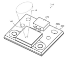
- FIG. 12A is a schematic cross-sectional view illustrating a method of attaching the cap unit 50 to the wiring board 20 according to the present embodiment.
- the semiconductor light emitting element 41 and the submount 45 are mounted on the wiring board 20 manufactured by the above-mentioned manufacturing method, and a metal wire (not shown) is attached in advance.
- FIG. 12A shows a cross section perpendicular to the wiring board 20 through the optical axis of the semiconductor light emitting device 41.
- FIG. 12B is a schematic cross-sectional view of a light source device using the semiconductor light emitting device 10 according to the present embodiment.
- the cap unit 50 since the top plate 52d of the cap unit 50 is transparent, as shown in FIG. 12A, the cap is not brought into contact with the side wall 51 which is a translucent window and the emission surface of the semiconductor light emitting element 41.
- the position of the unit 50 can be adjusted with high accuracy. For example, as shown in FIG. 12A, the position of the cap unit 50 is adjusted while observing an enlarged image of the cap unit 50 and the semiconductor light emitting element 41 from above the cap unit 50 using the image observation system 91. You may. This makes it possible to adjust the position of the cap unit 50 so that the distance between the side wall 51 and the exit surface of the semiconductor light emitting element 41 is less than the thickness of the side wall 51.
- the distance between the semiconductor light emitting element 41 and the outside of the cap unit 50 can be reduced.
- the wiring board 20 includes a spacer, and the wiring board 20 and the side wall 51 of the cap unit 50 are joined on the spacer.
- the amount of the bonding member between the wiring board 20 and the side wall 51 can be reduced, so that the excess bonding member reaches the vicinity of the adjacent semiconductor light emitting element 41 and changes the characteristics of the emitted light L1. It can be suppressed.
- a light source device including the semiconductor light emitting device 10 and the lens optical element 92 which is a fast-axis collimating lens.
- the distance DL between the emission surface of the semiconductor light emitting device 41 and the lens optical element 92 can be reduced.
- the beam width of the laser beam (emitted light L1) emitted from the semiconductor light emitting device 10 in the fast axis direction can be reduced.
- the distance obtained by adding the thickness Dg of the side wall 51 and the distance Dgap from the side wall 51 to the exit surface should be short.
- the lens optical element 92 can be brought closer to the emission surface of the semiconductor light emitting element 41 while maintaining the strength of the side wall 51.
- the semiconductor light emitting device 10 of the present embodiment can apply a large current to the semiconductor light emitting element 41 with a small wiring resistance to emit emitted light L1 having a large optical output. Since the semiconductor light emitting element 41 on the wiring board 20 is sealed by the cap unit 50, the reliability of the semiconductor light emitting element 41 can be improved. Further, the distance between the light emitting point 41e of the semiconductor light emitting element 41 and the outside of the cap unit 50 is reduced. Therefore, it is possible to more freely design an external optical element such as a lens optical element that is arranged outside the semiconductor light emitting device 10 and is optically coupled to the light emitting point 41e. Further, as shown in FIG.
- an oblique cut surface 28c is formed at the end portion of the metal substrate 28 of the wiring board on the upper surface 20a side.
- a part of the emitted light L1 can be suppressed from being kicked outside the semiconductor light emitting device, and the external optical element can be arranged more freely.
- the Joule heat generated in the semiconductor light emitting element 41 spreads on the metal substrate 28 and is radiated from the heat radiating surface 20b to the external heat sink. At this time, since the semiconductor light emitting device 41 is mounted on the metal substrate 28 without passing through the first insulating layer 21 and the second insulating layer 22, Joule heat is efficiently transferred to the metal substrate 28.
- the area of the lower surface of the metal substrate 28 is larger than the area of the upper surface due to the diagonally cut surface 28c at the end. Therefore, the Joule heat generated is transferred from the submount 45 to the metal substrate 28 as in the heat flows TP1 and TP5 shown in FIG. 4, and then spreads in a direction parallel to the upper surface of the metal substrate 28, resulting in efficiency. It is well dissipated to the outside. Therefore, the emitted light L1 having a higher light output can be emitted from the semiconductor light emitting element 41.
- the semiconductor light emitting device according to the first modification of the present embodiment will be described.
- the semiconductor light emitting device according to this modification is different from the semiconductor light emitting device 10 according to the first embodiment in the configuration of the spacer layer, and is the same in other configurations.
- the semiconductor light emitting device according to the present modification will be described with reference to FIG. 13A, focusing on the differences from the semiconductor light emitting device 10 according to the first embodiment.
- FIG. 13A is a schematic top view showing the configurations of the spacer layers 130a and 130b of the semiconductor light emitting device 110 according to this modification.
- FIG. 13A shows the configuration of the semiconductor light emitting device 41 of the semiconductor light emitting device 110 in a state where the cap unit 50 and the second insulating layer 22 are removed, and the periphery thereof.
- the spacer layers 130a and 130b according to this modification are made of the same material as the second metal layer 32, and are electrically connected to the second metal layer 32. More specifically, the spacer layers 130a and 130b and the second metal layer 32 have the same thickness, and the upper surfaces of the spacer layers and the second metal layer 32 are connected flat.
- each spacer layer and the second metal layer 32 are connected flush with each other.
- the boundary between the second metal layer 32 and each spacer layer may be appropriately set.
- the second metal layer 32 is defined as a rectangular portion extending in the optical axis direction.
- the spacer layer 130a is an edge of one of the second metal layers 32 (the side closer to the first metal layer 31) on the side of the rear end surface 41R on the side opposite to the emission surface 41F including the light emitting point 41e of the semiconductor light emitting element 41. Therefore, it is arranged so as to extend to the other side of the first metal layer 31 (the side closer to the second metal layer 32).
- the spacer layer 130a is a portion that protrudes from the second metal layer 32 in one direction (in the direction approaching the first metal layer 31).
- the spacer layer 130b is composed of five parts.
- the first portion of the spacer layer 130b is laterally (on the main surface of the wiring board 20) from the side of one of the first metal layers 31 (the side far from the second metal layer 32) on the side of the rear end surface 41R. In the plane, it is arranged so as to extend in the direction perpendicular to the optical axis direction).
- the second portion of the spacer layer 130b is connected to the first portion, and the optical axis is on the side of one of the first pad electrode 31p and the first metal layer 31 (the side far from the second metal layer 32).
- the third portion of the spacer layer 130b is connected to the second portion and is arranged so as to extend laterally on the side of the exit surface 41F.
- the fourth portion of the spacer layer 130b is connected to the third portion, and the optical axis is on the side of the second pad electrode 32p and the other side of the second metal layer 32 (the side far from the first metal layer 31).
- the fifth portion of the spacer layer 130b is connected to the fourth portion, and on the side of the rear end surface 41R, from the other end edge of the second metal layer 32 (the side far from the first metal layer 31). Arranged so as to extend laterally.
- Such spacer layers 130a and 130b can be formed at the same time as the second metal layer 32 in the step of forming each metal layer, similarly to the spacer layers according to the first embodiment. Even when each spacer layer is in contact with the second metal layer 32 as in this modification, each spacer layer is arranged at a position different from that of the second metal layer 32.
- the distance between the second metal layer 32 and each spacer layer is zero. Therefore, among the upper surfaces of the wiring board, the second metal layer 32 and each spacer layer No recess is formed at the corresponding position between and. Therefore, it is possible to reduce the formation of a gap between the joint surface 50b of the cap unit 50 and the upper surface of the wiring board. That is, the joint surface 50b of the cap unit 50 and the upper surface of the wiring board can be more reliably sealed.
- each spacer layer is connected to the second metal layer 32, but each spacer layer may be connected to the first metal layer 31.
- the spacer layers 130a and 130b may be made of the same material as the first metal layer 31. That is, the spacer layers 130a and 130b may be made of the same material as the first metal layer 31 or the second metal layer 32, and may be electrically connected to the first metal layer 31 or the second metal layer 32.
- the semiconductor light emitting device according to the second modification of the present embodiment will be described.
- the semiconductor light emitting device according to this modification is different from the semiconductor light emitting device 10 according to the first embodiment in the configuration of the spacer layer, and is the same in other configurations.
- the semiconductor light emitting device according to the present modification will be described with reference to FIG. 13B, focusing on the differences from the semiconductor light emitting device 10 according to the first embodiment.
- FIG. 13B is a schematic top view showing the configurations of the spacer layers 30a, 30b, and 30c of the semiconductor light emitting device 110a according to this modification.
- FIG. 13B shows the configuration of the semiconductor light emitting device 41 of the semiconductor light emitting device 110a in a state where the cap unit 50 and the second insulating layer 22 are removed, and the periphery thereof.
- the semiconductor light emitting device 110a according to the present modification includes four spacer layers 30c in addition to the spacer layers 30a and 30b similar to those in the first embodiment.
- the spacer layer 30c is an insulating film arranged between each metal layer and the spacer layers 30a and 30b.
- the spacer layer 30c for example, an inorganic material such as a resin or low melting point glass can be used.
- the spacer layers 30a and 30b are made of an insulating material
- the spacer layer 30c may be made of a metal material.
- the gap between each metal layer and the spacer layers 30a and 30b can be filled with the spacer layer 30c. Therefore, from the wiring board 20 according to the first embodiment, the wiring board The size of the recess formed on the upper surface can be reduced. Therefore, it is possible to reduce the formation of a gap between the joint surface 50b of the cap unit 50 and the upper surface of the wiring board. That is, the joint surface 50b of the cap unit 50 and the upper surface of the wiring board can be more reliably sealed.
- the thickness of the spacer layer 30c may be the same as that of each metal layer and the spacer layers 30a and 30b. As a result, the size of the recess formed on the upper surface of the wiring board can be further reduced.
- the semiconductor light emitting device according to the present modification is different from the semiconductor light emitting device 10 according to the first embodiment in that it includes a shielding member arranged between the temperature detecting element 60 and the semiconductor light emitting element 41, and other points. Matches in.
- the semiconductor light emitting device according to the present modification will be described with reference to FIGS. 14A and 14B, focusing on the differences from the semiconductor light emitting device 10 according to the first embodiment.
- 14A and 14B are schematic top views and sectional views showing the positional relationship between the semiconductor light emitting element 41, the temperature detecting element 60, and the shielding member 60s of the semiconductor light emitting device 110b according to this modification, respectively.
- 14B is a cross-sectional view of the semiconductor light emitting device 41 of FIG. 14A on the optical axis LA1.
- the semiconductor light emitting device 110b according to this modification includes a shielding member 60s arranged between the temperature detecting element 60 and the semiconductor light emitting element 41.
- the semiconductor light emitting device 41 also emits the emitted light L1B from the rear end surface 41R, which is the end surface opposite to the emission surface on which the light emitting point 41e is arranged.
- the intensity of the emitted light L1B is significantly smaller than that of the emitted light L1.
- the semiconductor light emitting device 41 is an element having a high light output, the intensity of the emitted light L1B is also relatively high. Therefore, when the emitted light L1B is applied to the temperature detecting element 60, the temperature of the temperature detecting element 60 rises, so that the temperature of the wiring board 20 cannot be accurately detected.
- the shielding member 60s is arranged between the temperature detecting element 60 and the rear end surface 41R of the semiconductor light emitting element 41.
- the semiconductor light emitting element 41, the shielding member 60s, and the temperature detecting element 60 are arranged in this order on the optical axis LA1.
- the shielding member 60s is not particularly limited as long as it can shield the emitted light L1B, but may be, for example, the same element as the temperature detecting element 60. When such an element is used as the shielding member 60s, no wiring is connected to the element.
- the dimension of the shielding member 60s may be larger than that of the temperature detecting element 60. As a result, it is possible to more reliably reduce the incident light L1B on the temperature detecting element 60.
- the shielding member 60s may be arranged outside the cap unit 50 or may be arranged inside.
- the semiconductor light emitting device according to the present embodiment is different from the semiconductor light emitting device 10 according to the first embodiment mainly in the configuration of the first metal layer and the second metal layer.
- the semiconductor light emitting device according to the present embodiment will be described focusing on the differences from the semiconductor light emitting device 10 according to the first embodiment.
- FIGS. 15 to 17 are a schematic perspective view and an exploded perspective view showing the overall configuration of the semiconductor light emitting device 210 according to the present embodiment, respectively.
- FIG. 17 is a schematic cross-sectional view showing the overall configuration of the semiconductor light emitting device 210 according to the present embodiment.
- FIG. 17 is a cross section along the XVII-XVII line of FIG. 16 and shows a cross section perpendicular to the upper surface 220a of the wiring board 220.
- the semiconductor light emitting device 210 includes a wiring board 220, a cap unit 50, and a connector 270. Further, as shown in FIGS. 16 and 17, the semiconductor light emitting device 210 further includes a semiconductor light emitting element 41, a submount 45, and a temperature detecting element 60. Further, as shown in FIG. 17, the semiconductor light emitting device 210 further includes joining members 226, 42, and 62, and a joining layer 255. Hereinafter, each component of the semiconductor light emitting device 210 will be described.
- the wiring board 220 includes a metal substrate 228, a first insulating layer 221, a second insulating layer 222, a third metal layer 233, and a fourth metal layer 234. And a protective film 225.
- the wiring board 20 includes a first metal layer 231 and a second metal layer 232, spacer layers 230a, 230b, and 230c, a first pad electrode 231p, and a second pad electrode. It further has 232p, a first take-out electrode 237, and a second take-out electrode 238.
- the wiring board 220 is formed with through holes 228a and 228b and positioning holes 229a and 229b.
- the through holes 228a and 228b and the positioning holes 229a and 229b according to the present embodiment are different from the through holes 28a and 28b and the positioning holes 29a and 29b according to the first embodiment in the arrangement on the wiring board 220.
- the positioning holes 229a and 229b are arranged near the rear end of the wiring board 220.
- the rear end of the wiring board 220 is the end of the wiring board 220 on the side farther from the light emitting point 41e among the two ends in the propagation direction of the emitted light L1.
- the side on which the emitted light L1 propagates with respect to the semiconductor light emitting device 41 is referred to as a front, and the opposite direction of the front is also referred to as a rear.
- the through holes 228a and 228b are arranged near the center of the wiring board 220 in the propagation direction of the emitted light L1.
- the metal substrate 228 is different from the metal substrate 28 according to the first embodiment in the number and arrangement of the holes provided, and is the same in terms of the points at the ends thereof.
- the first insulating layer 221 is an insulating layer having the same structure as the first insulating layer 21 according to the first embodiment, and an opening 221a is formed.
- the first metal layer 231 and the second metal layer 232, the third metal layer 233, and the fourth metal layer 234 are metal layers arranged apart from each other on the first insulating layer 221.
- the first metal layer 231 extends in a direction perpendicular to the propagation direction of the emitted light L1 from the first pad electrode 231p and parallel to the main surface of the metal substrate 228. , Is connected to the first take-out electrode 237.
- the first metal layer 231 extends from between the first pad electrode 231p and the first insulating layer 221 to between the first extraction electrode 237 and the first insulating layer 221. As shown in FIG.
- the second metal layer 232 extends in a direction perpendicular to the propagation direction of the emitted light L1 from the second pad electrode 232p and parallel to the main surface of the metal substrate 228, and the second extraction electrode 238. Connected to. Specifically, the second metal layer 232 extends from between the second pad electrode 232p and the first insulating layer 221 to between the second extraction electrode 238 and the first insulating layer 221. The second metal layer 232 is stretched in the direction opposite to the stretching direction of the first metal layer 231. As described above, in the present embodiment, the first metal layer 231 and the second metal layer 232 are not connected to the connector 270.
- the first metal layer 231 and the second metal layer 232 have a structure as shown in Design Example 6 of FIG. That is, the first metal layer 231 and the second metal layer 232 are copper films having a thickness T of 0.070 mm, a width W of 7.0 mm, and a length L of 5 mm. As a result, the resistance of the first metal layer 231 and the second metal layer 232 can be set to 0.0002 ⁇ . Therefore, even when a large current of about 30 A is supplied to the semiconductor light emitting device 41, the increase in the operating voltage due to the resistance of each metal layer can be suppressed to about 0.006 V.
- the third metal layer 233 and the fourth metal layer 234 are wirings connected to the temperature detecting element 60, similarly to the third metal layer 33 and the fourth metal layer 34 according to the first embodiment.
- the temperature detecting element 60 is arranged inside the cap unit 50, so that the wiring board 220 of the third metal layer 233 and the fourth metal layer 234 is used.
- the arrangement is different from the third metal layer 33 and the fourth metal layer 34 according to the first embodiment.
- the third metal layer 233 and the fourth metal layer 234 are in the optical axis direction on the side of the rear end surface 41R opposite to the emission surface 41F of the semiconductor light emitting device 41. Arranged to stretch to.
- the joint surface 50b joined to the wiring board 220 of the cap unit 50 intersects the third metal layer 233 and the fourth metal layer 234 in the top view of the wiring board 220.
- the first pad electrode 231p and the second pad electrode 232p have the same configurations as the first pad electrode 31p and the second pad electrode 32p according to the first embodiment, respectively.
- the spacer layers 230a, 230b, and 230c are layers arranged at different positions from the first metal layer 231 and the second metal layer 232 on the first insulating layer 221.
- the spacer layers 230a, 230b, and 230c are arranged between the joint surface 50b of the cap unit 50 with the wiring board 220 and the first insulating layer 221 in the same manner as in each spacer layer according to the first embodiment.
- Each spacer layer forms a convex portion on the first insulating layer 221 in the same manner as each metal layer.
- the spacer layer 230a has an L-shaped shape when viewed from above the wiring board 220, and is composed of two parts.
- the first portion of the spacer layer 230a is light from the rear end surface 41R side of the first metal layer 231 on the side of one of the semiconductor light emitting devices 41 (the side on which the first metal layer 231 of the semiconductor light emitting element 41 is arranged). Arranged so as to extend in the axial direction.
- the second portion of the spacer layer 230a is connected to the first portion and is arranged so as to extend laterally from one side of the third metal layer 233 on the side of the rear end surface 41R.
- the spacer layer 230b has an L-shape when viewed from above the wiring board 220, and is composed of two parts.
- the first portion of the spacer layer 230b is light from the rear end surface 41R side of the second metal layer 232 on the side of the other side of the semiconductor light emitting device 41 (the side where the second metal layer 232 of the semiconductor light emitting element 41 is arranged). Arranged so as to extend in the axial direction.
- the second portion of the spacer layer 230b is connected to the first portion and is arranged laterally extending laterally from the other side of the fourth metal layer 234 on the side of the rear end surface 41R.
- the spacer layer 230c is composed of three parts.
- the first portion of the spacer layer 230c is arranged so as to extend in the optical axis direction from the exit surface 41F side of the first metal layer 231 on one side of the semiconductor light emitting device 41.
- the second portion of the spacer layer 230c is connected to the first portion and is arranged so as to extend laterally on the side of the exit surface 41F.
- the third portion of the spacer layer 230c is connected to the second portion and extends in the optical axis direction from the exit surface 41F side of the second metal layer 232 on the other side of the semiconductor light emitting device 41. Be placed.
- the second insulating layer 222 is an insulating layer arranged on the first insulating layer 221 as shown in FIG.
- the second insulating layer 22 has the same as the second insulating layer 22 according to the first embodiment, that is, the first metal layer 231 and the second metal layer 232, the third metal layer 233, the fourth metal layer 234, and the spacer layer 230a. Covers 230b, and at least a portion of 230c.
- the protective film 225 is a metal film arranged at a position where the submount 45 is joined or the like on the wiring board 220.
- the protective film 225 is arranged in the region corresponding to the opening 221a of the first insulating layer 221 of the metal substrate 228, similarly to the protective film 25 according to the first embodiment.
- the protective film 235 is arranged on a part of the upper surface of the first metal layer 231, the second metal layer 232, the third metal layer 233, the fourth metal layer 234, and the like, similarly to the protective film 35 according to the first embodiment. Will be done.
- the submount 45 is arranged inside the opening 221a of the first insulating layer 221 and is mounted on the metal substrate 228 via the joining member 226 and the protective film 225.
- the joining member 226 is made of, for example, AuSn solder or the like.
- the first take-out electrode 237 and the second take-out electrode 238 are examples of take-out electrodes electrically connected to the first metal layer 231 and the second metal layer 232, respectively.
- the first take-out electrode 237 and the second take-out electrode 238 are arranged on the first metal layer 231 and the second metal layer 232, respectively.
- the first take-out electrode 237 and the second take-out electrode 238 are arranged in the vicinity of the first pad electrode 231p and the second pad electrode 232p, respectively.
- Each of the first take-out electrode 237 and the second take-out electrode 238 has an annular shape, and electrode through holes 237a and 238a penetrating the wiring board 220 are formed in the central portion, respectively.
- the through holes 228a and 228b are holes for inserting a fixing member such as a screw when the wiring board 220 is brought into close contact with the heat sink or the like and fixed.
- the electrode through holes 237a and 238a are arranged on one side and the other side on the opposite side of the region where the semiconductor light emitting element 41 of the wiring board 220 is arranged, respectively. In other words, the semiconductor light emitting device 41 is arranged between the electrode through holes 237a and the electrode through holes 238a.
- the joining layer 255 is a member that joins the joining surface 50b of the cap unit 50 and the upper surface 220a of the wiring board 220.
- the bonding layer 255 has a first bonding preliminary film 255a, a bonding member 255b, and a second bonding preliminary film 255c.
- the first bonding preliminary film 255a and the second bonding preliminary film 255c are metal films arranged on the bonding surface 50b and the upper surface of the second insulating layer 222, respectively, and are composed of Ni, Au, and the like. With these bonding preliminary films, the cap unit 50 and the second insulating layer 222 can be easily bonded by the bonding member 255b.
- the joining member 255b is an alloy member made of AuSn solder or the like.
- the temperature detection element 60 is the same element as the temperature detection element 60 according to the first embodiment.
- the temperature detecting element 60 is covered with the cap unit 50 as shown in FIGS. 16 and 17.
- the temperature detecting element 60 is not exposed to the outside air, and the influence of the outside air on the temperature detection is suppressed, so that the temperature can be detected with high accuracy.
- FIG. 18 is a top view showing the arrangement of the temperature detecting element 60 according to the present embodiment.
- the temperature detecting element 60 is arranged at a position that does not intersect with the optical axis LA1 of the semiconductor light emitting element 41. As a result, it is possible to prevent the temperature detecting element 60 from being irradiated with the emitted light L1B emitted from the rear end surface 41R of the semiconductor light emitting element 41 without arranging the shielding member. Therefore, the temperature of the wiring board 220 can be accurately detected by the temperature detecting element 60.
- the connector 270 is a connecting component having terminals connected to each of the third metal layer 233 and the fourth metal layer 234. In the present embodiment, unlike the connector 70 according to the first embodiment, the connector 270 does not have a terminal connected to the first metal layer 231 and the second metal layer 232.
- FIGS. 19A to 19C are schematic cross-sectional views illustrating a method of joining the cap unit 50 of the semiconductor light emitting device 210 according to the present embodiment to the wiring board 220.
- FIG. 19A shows a cross section similar to that in FIG. 17, but omits parts other than the wiring board 220 and the cap unit 50.
- 19B and 19C show the semiconductor light emitting device 210 in the cross section of the XIX-XIX line of FIG. 16 and perpendicular to the upper surface 220a of the wiring board 220.
- 19A and 19B show a state before joining the cap unit 50 and the wiring board 220
- FIG. 19C shows a state after joining the cap unit 50 and the wiring board 220.
- the first bonding preliminary film 255a and the bonding member 255b are formed on the bonding surface 50b of the cap unit 50 in this order.
- the second bonding preliminary film 255c is formed in the region of the upper surface 220a of the wiring board 220 facing the bonding surface 50b of the cap unit 50.
- the size of the recess formed on the upper surface 220a of the wiring board 220 can be reduced by each spacer layer, as in the first embodiment.
- the cap unit 50 is arranged on the upper surface 220a of the wiring board 220.
- the wiring board 220 is heated to melt the bonding member 255b between the first bonding preliminary film 255a and the second bonding preliminary film 255c.
- the joining member 255b is solidified by cooling the wiring board 220.
- the first bonding preliminary film 255a and the second bonding preliminary film 255c can be bonded by the bonding member 255b.
- the semiconductor light emitting device 210 having high light output and high reliability can be realized as in the first embodiment.
- FIGS. 20 and 21 are a schematic perspective view and an exploded perspective view showing the configuration of the light source device 201 according to the present embodiment, respectively.
- the light source device 201 includes a semiconductor light emitting device 210, a heat sink 219, terminal fixing screws S1 and S2, and fixing screws S3 and S4.
- the light source device 201 further comprises a cable 272 having a connector 271 and cables 211 and 212 having terminals 213 and 214, respectively.
- the heat sink 219 is a heat dissipation component made of a material having high thermal conductivity such as metal.
- the heat sink 219 is composed of, for example, iron, an iron alloy, aluminum, an aluminum alloy, copper, or the like. Further, a surface-treated aluminum alloy having an alumite-treated surface or copper having a Ni-plated surface may be used.
- the heat sink 219 is formed with positioning pins P1 and P2 and screw holes T1 to T4. The positioning pins P1 and P2 are inserted into the positioning holes 229a and 229b of the semiconductor light emitting device 210, respectively.
- the semiconductor light emitting device 210 is fixed in close contact with the heat sink 219 by using the terminal fixing screws S1 and S2 and the fixing screws S3 and S4. Specifically, the fixing screws S3 and S4 penetrate the through holes 228a and 228b of the wiring board, respectively, and are fixed to the screw holes T3 and T4 of the heat sink 219, respectively.
- the terminal fixing screw S1 penetrates the hole formed in the terminal 213 and the electrode through hole 237a of the wiring board 220, and is fixed to the screw hole T1 of the heat sink 219.
- the terminal fixing screw S1 penetrates the electrode through hole 237a, and the terminal 213 is arranged between the terminal fixing screw S1 and the first take-out electrode 237. As a result, the first extraction electrode 237 and the terminal 213 are electrically connected.
- the terminal fixing screw S2 is fixed to the screw hole T2 of the heat sink 219 via the hole formed in the terminal 214 and the electrode through hole 238a of the wiring board 220.
- the terminal fixing screw S2 penetrates the electrode through hole 238a, and the terminal 214 is arranged between the terminal fixing screw S2 and the second take-out electrode 238. As a result, the second extraction electrode 238 and the terminal 214 are electrically connected.
- the semiconductor light emitting device 210 can be fixed to the heat sink 219.
- the semiconductor light emitting device 210 can be firmly fixed to the heat sink 219 by using the terminal fixing screws S1 and S2, and the fixing screws S3 and S4, so that the heat generated by the semiconductor light emitting element 41 of the semiconductor light emitting device 210 can be generated. It can be effectively dissipated from the metal substrate 228 to the heat sink 219.
- the terminals 213 and 214 and the first take-out electrode 237 and the second take-out electrode 238 can be electrically connected, respectively. Therefore, a large current can be supplied to the semiconductor light emitting device 210 via the cables 211 and 212.
- the fixing screws S3 and S4 are made of, for example, a metal material.
- those made of an insulating material such as plastic or ceramic or those having an insulating coating are used in order to suppress a short circuit between each terminal and the metal substrate 228 and the heat sink.
- the connector 271 is connected to the connector 270. As a result, the signal from the temperature detecting element 60 can be acquired via the cable 272.
- FIG. 22A is a schematic cross-sectional view showing a state in which the terminal fixing screw Sc1 according to this modification is fixed to the heat sink 219.
- FIG. 22B is an exploded cross-sectional view showing a method of fixing the terminal fixing screw Sc1 according to the present modification to the heat sink 219.
- the surface of the heat sink 219 is conductive, for example, an aluminum alloy that has not been surface-treated.
- the terminal 213 and the wiring board 220 are fixed to the screw hole T1 of the heat sink 219 by using the terminal fixing screw Sc1 made of a conductive material such as iron or stainless steel.
- a ring-shaped washer Wi that is, a spacer
- an insulating material is inserted between the terminal fixing screw Sc1 and the terminal 213.
- the washer Wi is a washer with a brim with a brim WiC.
- a part of the washer Wi can be arranged inside the through hole of the terminal 213 or inside the electrode through hole 237a of the wiring board.
- the possibility that the terminal fixing screw Sc1 and the first take-out electrode 237 are short-circuited inside the hole can be reduced.
- the terminal 214 and the wiring board 220 can be fixed to the heat sink 219 made of a metal material with a terminal fixing screw made of a metal material.
- the semiconductor light emitting device 210 and the heat sink 219 can be fixed more firmly, and the semiconductor light emitting device 210 and the heat sink 219 can be brought into close contact with each other. Therefore, heat can be dissipated more efficiently from the semiconductor light emitting element 41 of the semiconductor light emitting device 210 to the heat sink 219.
- FIG. 25 shows the semiconductor light emitting device 310 in a part of the cross section in the XXV-XXV line of FIG. 23. Further, FIG. 25 shows a semiconductor light emitting device 310 in a state before the cap unit 350 is joined to the wiring board 220.
- the semiconductor light emitting device 310 includes a wiring board 220, a cap unit 350, and a connector 270. As shown in FIG. 24, the semiconductor light emitting device 310 further includes a semiconductor light emitting element 41, a submount 45, a reflection optical element 358, and a temperature detecting element 60. As shown in FIGS. 23 and 25, the semiconductor light emitting device 310 according to the present embodiment emits the emitted light L1 emitted by the semiconductor light emitting element 41 in a direction perpendicular to the upper surface 220a of the wiring board 220. Specifically, as shown in FIG.
- the semiconductor light emitting device 310 includes a reflecting optical element 358, and the light L1 emitted from the semiconductor light emitting element 41 is reflected by the reflecting optical element 358, and the upper surface of the wiring substrate 220 is formed. It propagates in the direction perpendicular to 220a.
- the reflective surface 358r of the reflective optical element 358 is arranged at a position facing the emission surface of the semiconductor light emitting element 41.
- the reflective surface 358r is inclined by 45 degrees with respect to the optical axis of the semiconductor light emitting device 41.
- the emitted light L1 is reflected by the reflecting surface 358r and propagates in the direction perpendicular to the upper surface 220a of the wiring board 220 and in the direction away from the wiring board 220.
- the reflective optical element 358 is bonded to the protective film 225 of the opening 221a via the bonding preliminary film 359 having the same configuration as the first bonding preliminary film 255a and the bonding member 226. ..
- the cap unit 350 has a transparent rectangular top plate 351 and a holder 352.
- the top plate 351 is a translucent window having the same configuration as the side wall 51 of the cap unit 50 according to the second embodiment. That is, the top plate 351 is a translucent window having an inorganic translucent plate and an antireflection film formed on the inorganic translucent plate. As a result, the light L1 emitted from the semiconductor light emitting device 41 passes through the top plate 351 which is a translucent window.
- the holder 352 is a frame-shaped member having four side walls connected to the four sides of the peripheral edge of the top plate 351.
- the emitted light L1 from the semiconductor light emitting device 41 can be easily taken out from the upper surface of the cap unit 350.
- the cap unit 350 is formed, for example, by joining the top plate 351 to the frame-shaped holder 352 by optical contact or laser welding. Therefore, the top plate 351 and the peripheral portion of the holder 352 are in close contact with each other. Further, a first bonding preliminary film (not shown) is arranged on the surface of the holder 352 facing the top plate 351.
- each spacer layer is arranged between the bonding surface of the wiring board 220 of the cap unit 350 with the upper surface 220a and the first insulating layer 221. Then, the second bonding preliminary film 255c is arranged on each spacer layer. Then, by adhering the holder 352 and the wiring board 220 with an adhesive, the space between the cap unit 350 and the wiring board 220 can be sealed. As a result, the semiconductor light emitting device 310 according to the present embodiment also has the same effect as the semiconductor light emitting device 210 according to the second embodiment.
- the same configuration as in the first embodiment may be adopted.
- the semiconductor light emitting device 310 includes one semiconductor light emitting device 41, but the semiconductor light emitting device 310 may include a plurality of semiconductor light emitting elements 41 (see a figure to be described later). 26).
- the reflective optical element may be arranged at a position facing each emission surface of the plurality of semiconductor light emitting elements 41.
- the plurality of semiconductor light emitting devices 41 may be arranged in an array or in a matrix.
- the reflective optical element having the reflecting surface inclined by 45 degrees with respect to the optical axis is arranged at the position facing the emission surface of the semiconductor light emitting element 41, but other optical elements are arranged. It is also good.
- a reflection optical element in which a wavelength conversion member made of a phosphor layer or the like is arranged on a reflection mirror surface inclined at any angle of 10 degrees or more and 80 degrees or less with respect to the optical axis may be arranged.
- the semiconductor light emitting device 41 for example, a semiconductor laser device using a nitride semiconductor material having a peak wavelength in a wavelength range in which the emitted light L1 is 380 nm or more and 490 nm or less may be used.
- a part of the emitted light L1 emitted from the semiconductor light emitting element 41 is wavelength-converted by the reflecting optical element, so that the light including a part of the emitted light L1 and the wavelength conversion light is converted into the semiconductor light emitting device 310. It can be emitted from the top plate 351 of the above. More specifically, the emitted light L1 may be light having a wavelength in the blue region, and the wavelength conversion light may be light having a wavelength in the yellow region. As a result, it is possible to realize a highly reliable semiconductor light emitting device that emits white light having high brightness and high light output from the top plate 351.
- the reflection optical element a diffraction optical element or a diffusion optical element may be used.
- the light L1 emitted from the semiconductor light emitting element 41 can be emitted from the top plate 351 in an arbitrary direction by the reflecting optical element in a predetermined emission pattern.
- the emitted light L1 having a wavelength in the 900 nm band it is possible to realize a semiconductor light emitting device 310 that emits high-output infrared light and has high reliability.
- Such a semiconductor light emitting device 310 can be used, for example, in a Lidar (light detection and ranking) device or the like.
- the semiconductor light emitting device includes a plurality of semiconductor light emitting elements. Then, the reflective optical element is arranged at a position facing each emission surface of the plurality of semiconductor light emitting elements 41. The plurality of semiconductor light emitting elements 41 and the reflecting optical elements are arranged in a matrix.
- the configuration of the semiconductor light emitting device according to this modification will be described with reference to FIG. 26.
- FIG. 26 is a schematic top view showing the overall configuration of the semiconductor light emitting device 310b according to this modification. Note that FIG. 26 shows a state before the cap unit is attached to the wiring board 320b in order to show the inside of the cap unit. Therefore, the second bonding preliminary film 355c arranged along the bonding surface of the cap unit is shown. In this modification, the plurality of semiconductor light emitting elements 41 and the reflecting optical elements 358 are arranged in a matrix of 3 rows and 3 columns.
- the semiconductor light emitting device 310b includes a wiring substrate 320b, a plurality of semiconductor light emitting elements 41, a plurality of submounts 45, a cap unit (not shown in FIG. 26), a temperature detecting element 60, and a connector. 371 and 372 are provided.
- the wiring board 320b includes a metal substrate (not shown in FIG. 26), a first insulating layer 321, first metal layers 331a to 331c, second metal layers 332a to 332c, a third metal layer 333, and a third metal layer. It has four metal layers 334, spacer layers 530a to 530i, a plurality of first pad electrodes 331p, a plurality of second pad electrodes 332p, and a second insulating layer 322.
- the wiring board 320b is formed with positioning holes 229a and 229b and through holes 228a to 228d.
- the first insulating layer 321 is arranged on a metal substrate, and an opening 321a is formed.
- the first metal layers 331a to 331c are arranged on the first insulating layer 321 and are connected to the first pad electrode 331p and the connector 371.
- the second metal layers 332a to 332c are arranged on the first insulating layer 321 and are connected to the second pad electrode 332p and the connector 372.
- the third metal layer 333 is arranged on the first insulating layer 321 and is connected to the temperature detecting element 60 and the connector 371.
- the fourth metal layer 334 is arranged on the first insulating layer 321 and is connected to the temperature detecting element 60 and the connector 372.
- the second insulating layer 322 is arranged on the first insulating layer 321 and covers at least a part of each first metal layer, each second metal layer, and each spacer layer.
- the spacer layers 530a to 530i are arranged at different positions from the first metal layer and the second metal layer between the joint surface of the cap unit and the top of the first insulating layer 321. Also in this modification, each spacer layer is arranged along the joint surface of the cap unit.
- the semiconductor light emitting element 41 is mounted on the submount 45.
- the three semiconductor light emitting devices arranged in the same row (that is, arranged in the left-right direction in FIG. 26) are electrically connected in series by the metal wire W1.
- the first pad electrode 331p and the second pad electrode 332p are arranged in the lateral direction (horizontal direction in FIG. 26) of the semiconductor light emitting elements 41 arranged in the three row directions. That is, a plurality of semiconductor light emitting elements 41 electrically directly connected are arranged side by side between the first pad electrode 331p and the second pad electrode 332p.
- three semiconductor light emitting elements 41 are arranged in the row direction.
- Three first pad electrodes 331p and three second pad electrodes 332p are arranged in the row direction, and are provided so as to correspond to a plurality of semiconductor light emitting element groups in the three rows.
- Each first pad electrode 331p is connected to the semiconductor light emitting device 41 by a metal wire W2.
- Each second pad electrode 332p is connected to the semiconductor light emitting device 41 by a metal wire W3.
- the plurality of first pad electrodes 331p and the second pad electrodes 332p are provided at opposite positions on the wiring board 320b by the corresponding plurality of first metal layers 331a to 331c and the second metal layers 332a to 332c, respectively. It is connected to the two connectors 371 and 372.
- the light output of the emitted light emitted from the semiconductor light emitting device 310b can be increased as compared with the case where a single semiconductor light emitting element 41 is used. Further, as the light output increases, the heat generated by the semiconductor light emitting device 410 also increases, but according to the semiconductor light emitting device 310b according to this modification, heat can be efficiently exhausted by using a heat sink or the like. Deterioration of the semiconductor light emitting device can be suppressed. Therefore, it is possible to realize a semiconductor light emitting device 310b having high light output and high reliability.
- Such a semiconductor light emitting device 310b can be used as a light source for a projector or the like by using, for example, a semiconductor laser element or the like that emits emitted light having a wavelength in the visible light region such as blue, green, or red as the semiconductor light emitting element 41. Can be used.
- the semiconductor light emitting device according to the present embodiment is different from the semiconductor light emitting device 10 according to the first embodiment in that it includes a plurality of semiconductor light emitting elements.
- the semiconductor light emitting device according to the present embodiment will be described with reference to FIG. 27, focusing on the differences from the semiconductor light emitting device 10 according to the first embodiment.
- FIG. 27 is a schematic top view showing the overall configuration of the semiconductor light emitting device 410 according to the present embodiment. Note that FIG. 27 shows a state before the cap unit is attached to the wiring board 420 in order to show the inside of the cap unit 450. Therefore, the second bonding preliminary film 455c arranged along the bonding surface of the cap unit is shown.
- the semiconductor light emitting device 410 includes a wiring substrate 420, a cap unit 450, semiconductor light emitting elements 441a to 441c, a submount 445, a temperature detecting element 60, a shielding member 60s, and a connector 70. Be prepared.
- the cap unit 450, the temperature detection element 60, and the connector 70 have the same configurations as the cap unit 50, the temperature detection element 60, and the connector 70 according to the first embodiment, respectively.
- the cap unit 450 has a side wall 451 which is a translucent window.
- the shielding member 60s has the same configuration as the shielding member 60s according to the third modification of the first embodiment.
- the temperature detecting element 60 and the shielding member 60s are arranged inside the cap unit 450.
- the wiring board 420 includes a metal substrate 428, a first insulating layer 421, a second insulating layer 422, spacer layers 430a, 430b, 430c, and 430d.
- the spacer layers 430a, 430b, 430c, and 430d, the first metal layer 431, the second metal layer 432, the third metal layer 433, and the fourth metal layer 434 are the second insulating layer 422. Since it is hidden underneath, it is shown by a broken line.
- the wiring board 420 is formed with through holes 428a and 428b and positioning holes 429a and 429b, similarly to the wiring board 20 according to the first embodiment.
- An opening 421a is formed in the first insulating layer as in the first insulating layer 21 according to the first embodiment.
- a protective film made of Ni, Au, or the like is formed in the opening 421a, and a mounting surface for mounting each semiconductor light emitting device is formed.
- the semiconductor light emitting elements 441a to 441c are arranged in the opening via the submount 445.
- the first metal layer 431, the second metal layer 432, the third metal layer 433, and the fourth metal layer 434, the first pad electrode 431p, and the second pad electrode 432p are the first metal according to the first embodiment, respectively. It has the same configuration as the layer 431, the second metal layer 432, the third metal layer 433, the fourth metal layer 434, the first pad electrode 31p, and the second pad electrode 32p.
- the spacer layers 430a, 430b, 430c, and 430d according to the present embodiment have the joint surface of the cap unit 450 with the wiring board 420 and the first wiring board 420, similarly to the spacer layers according to the first embodiment. It is placed between the insulating layer. In the present embodiment, the spacer layer is arranged at a position different from each metal layer on the first insulating layer. As a result, the semiconductor light emitting device 410 according to the present embodiment also has the same effect as the semiconductor light emitting device 10 according to the first embodiment.
- the submount 445 includes an insulating block which is a rectangular parallelepiped block made of an insulating material, first electrodes 447a to 447c which are metal films arranged on the upper surface of the insulating block, and second electrodes 448, and the insulating block. It has a metal film (not shown) arranged on the lower surface.
- the first electrodes 447a to 447c and the second electrode 448 are arranged apart from each other and are electrically insulated. Further, the first electrodes 447a to 447c and the second electrode 448 are electrically insulated from the metal film arranged on the lower surface of the insulating block.
- the metal film arranged on the lower surfaces of the first electrodes 447a to 447c, the second electrode 448, and the insulating block is a metal film made of Ni, Cu, Pi, Au, or the like.
- Each of the semiconductor light emitting devices 441a to 441c has the same configuration as the semiconductor light emitting device 41 according to the first embodiment.
- the semiconductor light emitting devices 441a to 441c are junction-down mounted on the first electrodes 447a to 447c, respectively.
- first pad electrode 431p and the first electrode 447a are connected by a metal wire W2.
- the upper surface of the semiconductor light emitting device 441a and the first electrode 447b are connected by a metal wire W1.
- the upper surface of the semiconductor light emitting device 441b and the first electrode 447c are connected by a metal wire W1.
- the upper surface of the semiconductor light emitting device 441c and the second electrode 448 are connected by a metal wire W1.
- the second electrode 448 and the second pad electrode 432p are connected by a metal wire W3.
- the optical output of the emitted light emitted from the semiconductor light emitting device 410 can be increased as compared with the case where a single semiconductor light emitting element 41 is used. Further, as the light output increases, the heat generated by the semiconductor light emitting device 410 also increases, but according to the semiconductor light emitting device 410 according to the present embodiment, heat can be efficiently exhausted by using a heat sink or the like. Deterioration of each semiconductor light emitting device can be suppressed.
- the semiconductor light emitting device is a semiconductor light emitting device
- the semiconductor light emitting device is not limited to the semiconductor light emitting device.
- the semiconductor light emitting device may be a superluminescent diode or a quantum cascade laser.
- the first substrate may be an insulating substrate.
- the wiring board does not have to have the first insulating layer.
- the temperature detection element is used as an example of the functional element, but other functional elements may be used.
- functional elements for example, light-receiving elements, switching elements such as transistors, various passive elements such as capacitors, inductors, and resistors can also be used.
- the shape of the metal layer or the pad electrode connected to the functional element can be arbitrarily selected according to the type of the functional element and the like.
- the semiconductor light emitting element and the functional element may be electrically connected on the wiring board.
- the semiconductor light emitting device includes the shielding member 60s, but when the temperature detecting element 60 is arranged outside the cap unit 50, the cap unit 50 is a shielding member. May function as. That is, among the four side walls of the cap unit 50, the cap unit 50 functions as a shielding member by reducing the transmittance of light from the semiconductor light emitting element 41 on the side wall facing the rear end surface 41R of the semiconductor light emitting element 41. be able to.
- the semiconductor light emitting device is mounted on the metal substrate via the submount, but may be directly mounted without the submount.
- the semiconductor light emitting device may be mounted on a metal substrate at a junction up.
- FIG. 28 is a schematic perspective view showing the configuration of the semiconductor light emitting device 910 according to the reference example.
- the semiconductor light emitting device 910 includes a wiring board 920, a semiconductor light emitting element 41, a submount 45, a temperature detecting element 60, and a connector 70.
- the semiconductor light emitting device 41, the submount 45, the temperature detecting element 60, and the connector 70 have the same configurations as the semiconductor light emitting element 41, the submount 45, the temperature detecting element 60, and the connector 70 according to the first embodiment.
- the wiring board 920 is different from the wiring board 20 according to the first embodiment in that the configuration of the first insulating layer 921, the configuration of the third metal layer 933 and the fourth metal layer 934, and the spacer layer are not provided. , Other configurations match.
- the opening 921a of the first insulating layer 921 extends to the edge of the wiring board 920. That is, the opening 921a has an opening shape in the first insulating layer 921 that is open on the side surface side in the emission direction of the emission light L1 of the semiconductor light emitting element 41.
- the third metal layer 933 and the fourth metal layer 934 have the same configurations as the third metal layer 233 and the fourth metal layer 234 according to the second embodiment, respectively.
- the second insulating layer 922 has the same configuration as the second insulating layer 222 according to the second embodiment.
- a semiconductor light emitting device having a high light output can also be realized by a semiconductor light emitting device 910 having a configuration that does not have such a cap unit. Further, since the semiconductor light emitting device 910 does not include the cap unit and the spacer layer, the semiconductor light emitting device 910 has a simpler configuration than the semiconductor light emitting device 10 according to the first embodiment, and has a high degree of freedom in design.
- the semiconductor light emitting device and the like of the present disclosure include, for example, a laser processing machine, a vehicle lighting device such as a vehicle headlight, a distance measuring device such as a lighting device and a lidar device, and a light source for a projector as a light source having high light output and high reliability. It can be applied to devices, medical light source devices, inspection light source devices, sterilization light source devices, and the like.
Landscapes
- Physics & Mathematics (AREA)
- Condensed Matter Physics & Semiconductors (AREA)
- General Physics & Mathematics (AREA)
- Electromagnetism (AREA)
- Optics & Photonics (AREA)
- Led Device Packages (AREA)
Priority Applications (2)
| Application Number | Priority Date | Filing Date | Title |
|---|---|---|---|
| JP2022544463A JP7736696B2 (ja) | 2020-08-25 | 2021-08-16 | 半導体発光装置及び光源装置 |
| US18/172,120 US20230198221A1 (en) | 2020-08-25 | 2023-02-21 | Semiconductor light-emitting device and light source device |
Applications Claiming Priority (2)
| Application Number | Priority Date | Filing Date | Title |
|---|---|---|---|
| JP2020141924 | 2020-08-25 | ||
| JP2020-141924 | 2020-08-25 |
Related Child Applications (1)
| Application Number | Title | Priority Date | Filing Date |
|---|---|---|---|
| US18/172,120 Continuation US20230198221A1 (en) | 2020-08-25 | 2023-02-21 | Semiconductor light-emitting device and light source device |
Publications (1)
| Publication Number | Publication Date |
|---|---|
| WO2022044865A1 true WO2022044865A1 (ja) | 2022-03-03 |
Family
ID=80354205
Family Applications (1)
| Application Number | Title | Priority Date | Filing Date |
|---|---|---|---|
| PCT/JP2021/029884 Ceased WO2022044865A1 (ja) | 2020-08-25 | 2021-08-16 | 半導体発光装置及び光源装置 |
Country Status (3)
| Country | Link |
|---|---|
| US (1) | US20230198221A1 (https=) |
| JP (1) | JP7736696B2 (https=) |
| WO (1) | WO2022044865A1 (https=) |
Cited By (1)
| Publication number | Priority date | Publication date | Assignee | Title |
|---|---|---|---|---|
| WO2025183158A1 (ja) * | 2024-02-28 | 2025-09-04 | 京セラ株式会社 | 光素子搭載用パッケージ及び発光装置 |
Families Citing this family (1)
| Publication number | Priority date | Publication date | Assignee | Title |
|---|---|---|---|---|
| US20230238770A1 (en) * | 2022-01-24 | 2023-07-27 | Materion Corporation | Semiconductor package for an edge emitting laser diode |
Citations (7)
| Publication number | Priority date | Publication date | Assignee | Title |
|---|---|---|---|---|
| JP2004087543A (ja) * | 2002-08-23 | 2004-03-18 | Furukawa Electric Co Ltd:The | 光モジュール |
| US20050275075A1 (en) * | 2004-06-11 | 2005-12-15 | Suk-Kee Hong | Micro-electro-mechanical system (MEMS) package with spacer for sealing and method of manufacturing the same |
| JP2011112737A (ja) * | 2009-11-25 | 2011-06-09 | Oki Data Corp | 表示パネル、表示パネルの製造方法、及び表示装置 |
| WO2011142059A1 (ja) * | 2010-05-12 | 2011-11-17 | パナソニック株式会社 | 半導体装置及びその製造方法 |
| JP2013156556A (ja) * | 2012-01-31 | 2013-08-15 | Oki Data Corp | 表示パネル、表示パネルの製造方法、及び表示装置 |
| JP2013157364A (ja) * | 2012-01-27 | 2013-08-15 | Oki Data Corp | 発光パネル、及びそれを備えたヘッドアップディスプレイ |
| JP2018106973A (ja) * | 2016-12-27 | 2018-07-05 | 大日本印刷株式会社 | Ledバックライト装置およびled画像表示装置 |
Family Cites Families (3)
| Publication number | Priority date | Publication date | Assignee | Title |
|---|---|---|---|---|
| JP2007005505A (ja) * | 2005-06-23 | 2007-01-11 | Matsushita Electric Ind Co Ltd | 半導体レーザ装置 |
| JP2009088066A (ja) * | 2007-09-28 | 2009-04-23 | Panasonic Corp | 半導体装置 |
| JP5127594B2 (ja) * | 2008-06-26 | 2013-01-23 | 三菱電機株式会社 | 半導体パッケージ |
-
2021
- 2021-08-16 JP JP2022544463A patent/JP7736696B2/ja active Active
- 2021-08-16 WO PCT/JP2021/029884 patent/WO2022044865A1/ja not_active Ceased
-
2023
- 2023-02-21 US US18/172,120 patent/US20230198221A1/en active Pending
Patent Citations (7)
| Publication number | Priority date | Publication date | Assignee | Title |
|---|---|---|---|---|
| JP2004087543A (ja) * | 2002-08-23 | 2004-03-18 | Furukawa Electric Co Ltd:The | 光モジュール |
| US20050275075A1 (en) * | 2004-06-11 | 2005-12-15 | Suk-Kee Hong | Micro-electro-mechanical system (MEMS) package with spacer for sealing and method of manufacturing the same |
| JP2011112737A (ja) * | 2009-11-25 | 2011-06-09 | Oki Data Corp | 表示パネル、表示パネルの製造方法、及び表示装置 |
| WO2011142059A1 (ja) * | 2010-05-12 | 2011-11-17 | パナソニック株式会社 | 半導体装置及びその製造方法 |
| JP2013157364A (ja) * | 2012-01-27 | 2013-08-15 | Oki Data Corp | 発光パネル、及びそれを備えたヘッドアップディスプレイ |
| JP2013156556A (ja) * | 2012-01-31 | 2013-08-15 | Oki Data Corp | 表示パネル、表示パネルの製造方法、及び表示装置 |
| JP2018106973A (ja) * | 2016-12-27 | 2018-07-05 | 大日本印刷株式会社 | Ledバックライト装置およびled画像表示装置 |
Cited By (1)
| Publication number | Priority date | Publication date | Assignee | Title |
|---|---|---|---|---|
| WO2025183158A1 (ja) * | 2024-02-28 | 2025-09-04 | 京セラ株式会社 | 光素子搭載用パッケージ及び発光装置 |
Also Published As
| Publication number | Publication date |
|---|---|
| US20230198221A1 (en) | 2023-06-22 |
| JP7736696B2 (ja) | 2025-09-09 |
| JPWO2022044865A1 (https=) | 2022-03-03 |
Similar Documents
| Publication | Publication Date | Title |
|---|---|---|
| EP4220874B1 (en) | Light emitting device | |
| US10411168B2 (en) | Semiconductor component having a small structural height | |
| US20060022216A1 (en) | Semiconductor light-emitting device and method of manufacturing the same | |
| CN101365907B (zh) | 照明系统和显示设备 | |
| KR20180011024A (ko) | 레이저 컴포넌트 | |
| US11309680B2 (en) | Light source device including lead terminals that cross space defined by base and cap | |
| EP3583667B1 (en) | Bonded laser with solder-free laser active stripe in facing relationship with submount | |
| US20230198221A1 (en) | Semiconductor light-emitting device and light source device | |
| US12568723B2 (en) | Semiconductor light-emitting device and light source device including the same | |
| JP2009064961A (ja) | 半導体レーザ装置およびその製造方法 | |
| US20250287749A1 (en) | Light-emitting device and method for manufacturing light-emitting device | |
| JP7583321B2 (ja) | 光源装置 | |
| CN114026752A (zh) | 半导体激光装置 | |
| US11973317B2 (en) | Semiconductor laser and projector | |
| CN112636160A (zh) | 激光器 | |
| JP7371642B2 (ja) | 半導体発光デバイス | |
| CN111739844A (zh) | 一种芯片及芯片封装方法、电子设备 | |
| US20250030219A1 (en) | Laser component and method for producing a laser component | |
| JP5351624B2 (ja) | Ledモジュール | |
| JPH06260723A (ja) | 半導体レーザ装置 | |
| KR20190142576A (ko) | 표면발광 레이저패키지 및 이를 포함하는 광 모듈 | |
| US20240250497A1 (en) | Light emitting device | |
| WO2022027470A1 (zh) | 一种芯片及芯片封装方法、电子设备 | |
| JP2021125657A (ja) | 半導体レーザ装置 | |
| JP4771872B2 (ja) | 半導体レーザ光源装置およびそれを用いた通信機器ならびに照明機器 |
Legal Events
| Date | Code | Title | Description |
|---|---|---|---|
| 121 | Ep: the epo has been informed by wipo that ep was designated in this application |
Ref document number: 21861293 Country of ref document: EP Kind code of ref document: A1 |
|
| ENP | Entry into the national phase |
Ref document number: 2022544463 Country of ref document: JP Kind code of ref document: A |
|
| NENP | Non-entry into the national phase |
Ref country code: DE |
|
| 122 | Ep: pct application non-entry in european phase |
Ref document number: 21861293 Country of ref document: EP Kind code of ref document: A1 |