WO2022044522A1 - 基板処理方法、および基板処理装置 - Google Patents
基板処理方法、および基板処理装置 Download PDFInfo
- Publication number
- WO2022044522A1 WO2022044522A1 PCT/JP2021/024080 JP2021024080W WO2022044522A1 WO 2022044522 A1 WO2022044522 A1 WO 2022044522A1 JP 2021024080 W JP2021024080 W JP 2021024080W WO 2022044522 A1 WO2022044522 A1 WO 2022044522A1
- Authority
- WO
- WIPO (PCT)
- Prior art keywords
- filler
- substrate
- gap
- wafer
- substrate processing
- Prior art date
Links
- 239000000758 substrate Substances 0.000 title claims abstract description 189
- 238000012545 processing Methods 0.000 title claims abstract description 45
- 238000003672 processing method Methods 0.000 title claims abstract description 16
- 239000000945 filler Substances 0.000 claims abstract description 144
- 230000002093 peripheral effect Effects 0.000 claims abstract description 94
- 238000005304 joining Methods 0.000 claims abstract description 13
- 229920001187 thermosetting polymer Polymers 0.000 claims abstract description 7
- 230000007246 mechanism Effects 0.000 claims description 44
- 239000011248 coating agent Substances 0.000 claims description 40
- 238000000576 coating method Methods 0.000 claims description 40
- 238000002347 injection Methods 0.000 claims description 39
- 239000007924 injection Substances 0.000 claims description 39
- 230000007723 transport mechanism Effects 0.000 claims description 12
- 230000003287 optical effect Effects 0.000 claims description 9
- 238000005336 cracking Methods 0.000 abstract description 12
- 238000000034 method Methods 0.000 abstract description 6
- 235000012431 wafers Nutrition 0.000 description 132
- 239000007789 gas Substances 0.000 description 26
- 238000010586 diagram Methods 0.000 description 14
- IJGRMHOSHXDMSA-UHFFFAOYSA-N Atomic nitrogen Chemical compound N#N IJGRMHOSHXDMSA-UHFFFAOYSA-N 0.000 description 5
- 229910001873 dinitrogen Inorganic materials 0.000 description 5
- 238000010438 heat treatment Methods 0.000 description 5
- 238000005192 partition Methods 0.000 description 5
- 238000000227 grinding Methods 0.000 description 4
- 238000012546 transfer Methods 0.000 description 4
- 238000004891 communication Methods 0.000 description 3
- 230000008569 process Effects 0.000 description 3
- 230000015572 biosynthetic process Effects 0.000 description 2
- 238000005516 engineering process Methods 0.000 description 2
- 239000000463 material Substances 0.000 description 2
- 239000004065 semiconductor Substances 0.000 description 2
- 230000009471 action Effects 0.000 description 1
- 238000011161 development Methods 0.000 description 1
- 230000003028 elevating effect Effects 0.000 description 1
- 238000004519 manufacturing process Methods 0.000 description 1
- 238000012986 modification Methods 0.000 description 1
- 230000004048 modification Effects 0.000 description 1
- 238000005498 polishing Methods 0.000 description 1
- 238000003825 pressing Methods 0.000 description 1
- 230000002250 progressing effect Effects 0.000 description 1
- 229920005989 resin Polymers 0.000 description 1
- 239000011347 resin Substances 0.000 description 1
Images


Classifications
-
- H—ELECTRICITY
- H01—ELECTRIC ELEMENTS
- H01L—SEMICONDUCTOR DEVICES NOT COVERED BY CLASS H10
- H01L21/00—Processes or apparatus adapted for the manufacture or treatment of semiconductor or solid state devices or of parts thereof
- H01L21/67—Apparatus specially adapted for handling semiconductor or electric solid state devices during manufacture or treatment thereof; Apparatus specially adapted for handling wafers during manufacture or treatment of semiconductor or electric solid state devices or components ; Apparatus not specifically provided for elsewhere
- H01L21/67005—Apparatus not specifically provided for elsewhere
- H01L21/67011—Apparatus for manufacture or treatment
- H01L21/67092—Apparatus for mechanical treatment
-
- H—ELECTRICITY
- H01—ELECTRIC ELEMENTS
- H01L—SEMICONDUCTOR DEVICES NOT COVERED BY CLASS H10
- H01L21/00—Processes or apparatus adapted for the manufacture or treatment of semiconductor or solid state devices or of parts thereof
- H01L21/02—Manufacture or treatment of semiconductor devices or of parts thereof
- H01L21/04—Manufacture or treatment of semiconductor devices or of parts thereof the devices having at least one potential-jump barrier or surface barrier, e.g. PN junction, depletion layer or carrier concentration layer
- H01L21/18—Manufacture or treatment of semiconductor devices or of parts thereof the devices having at least one potential-jump barrier or surface barrier, e.g. PN junction, depletion layer or carrier concentration layer the devices having semiconductor bodies comprising elements of Group IV of the Periodic System or AIIIBV compounds with or without impurities, e.g. doping materials
- H01L21/185—Joining of semiconductor bodies for junction formation
- H01L21/187—Joining of semiconductor bodies for junction formation by direct bonding
-
- H—ELECTRICITY
- H01—ELECTRIC ELEMENTS
- H01L—SEMICONDUCTOR DEVICES NOT COVERED BY CLASS H10
- H01L21/00—Processes or apparatus adapted for the manufacture or treatment of semiconductor or solid state devices or of parts thereof
- H01L21/02—Manufacture or treatment of semiconductor devices or of parts thereof
- H01L21/04—Manufacture or treatment of semiconductor devices or of parts thereof the devices having at least one potential-jump barrier or surface barrier, e.g. PN junction, depletion layer or carrier concentration layer
- H01L21/50—Assembly of semiconductor devices using processes or apparatus not provided for in a single one of the subgroups H01L21/06 - H01L21/326, e.g. sealing of a cap to a base of a container
- H01L21/56—Encapsulations, e.g. encapsulation layers, coatings
-
- H—ELECTRICITY
- H01—ELECTRIC ELEMENTS
- H01L—SEMICONDUCTOR DEVICES NOT COVERED BY CLASS H10
- H01L21/00—Processes or apparatus adapted for the manufacture or treatment of semiconductor or solid state devices or of parts thereof
- H01L21/02—Manufacture or treatment of semiconductor devices or of parts thereof
- H01L21/02002—Preparing wafers
-
- H—ELECTRICITY
- H01—ELECTRIC ELEMENTS
- H01L—SEMICONDUCTOR DEVICES NOT COVERED BY CLASS H10
- H01L21/00—Processes or apparatus adapted for the manufacture or treatment of semiconductor or solid state devices or of parts thereof
- H01L21/02—Manufacture or treatment of semiconductor devices or of parts thereof
- H01L21/04—Manufacture or treatment of semiconductor devices or of parts thereof the devices having at least one potential-jump barrier or surface barrier, e.g. PN junction, depletion layer or carrier concentration layer
- H01L21/18—Manufacture or treatment of semiconductor devices or of parts thereof the devices having at least one potential-jump barrier or surface barrier, e.g. PN junction, depletion layer or carrier concentration layer the devices having semiconductor bodies comprising elements of Group IV of the Periodic System or AIIIBV compounds with or without impurities, e.g. doping materials
- H01L21/185—Joining of semiconductor bodies for junction formation
-
- H—ELECTRICITY
- H01—ELECTRIC ELEMENTS
- H01L—SEMICONDUCTOR DEVICES NOT COVERED BY CLASS H10
- H01L21/00—Processes or apparatus adapted for the manufacture or treatment of semiconductor or solid state devices or of parts thereof
- H01L21/67—Apparatus specially adapted for handling semiconductor or electric solid state devices during manufacture or treatment thereof; Apparatus specially adapted for handling wafers during manufacture or treatment of semiconductor or electric solid state devices or components ; Apparatus not specifically provided for elsewhere
- H01L21/67005—Apparatus not specifically provided for elsewhere
- H01L21/67011—Apparatus for manufacture or treatment
- H01L21/67098—Apparatus for thermal treatment
- H01L21/67109—Apparatus for thermal treatment mainly by convection
-
- H—ELECTRICITY
- H01—ELECTRIC ELEMENTS
- H01L—SEMICONDUCTOR DEVICES NOT COVERED BY CLASS H10
- H01L21/00—Processes or apparatus adapted for the manufacture or treatment of semiconductor or solid state devices or of parts thereof
- H01L21/67—Apparatus specially adapted for handling semiconductor or electric solid state devices during manufacture or treatment thereof; Apparatus specially adapted for handling wafers during manufacture or treatment of semiconductor or electric solid state devices or components ; Apparatus not specifically provided for elsewhere
- H01L21/67005—Apparatus not specifically provided for elsewhere
- H01L21/67011—Apparatus for manufacture or treatment
- H01L21/67098—Apparatus for thermal treatment
- H01L21/67115—Apparatus for thermal treatment mainly by radiation
-
- H—ELECTRICITY
- H01—ELECTRIC ELEMENTS
- H01L—SEMICONDUCTOR DEVICES NOT COVERED BY CLASS H10
- H01L21/00—Processes or apparatus adapted for the manufacture or treatment of semiconductor or solid state devices or of parts thereof
- H01L21/67—Apparatus specially adapted for handling semiconductor or electric solid state devices during manufacture or treatment thereof; Apparatus specially adapted for handling wafers during manufacture or treatment of semiconductor or electric solid state devices or components ; Apparatus not specifically provided for elsewhere
- H01L21/67005—Apparatus not specifically provided for elsewhere
- H01L21/67011—Apparatus for manufacture or treatment
- H01L21/6715—Apparatus for applying a liquid, a resin, an ink or the like
-
- H—ELECTRICITY
- H01—ELECTRIC ELEMENTS
- H01L—SEMICONDUCTOR DEVICES NOT COVERED BY CLASS H10
- H01L21/00—Processes or apparatus adapted for the manufacture or treatment of semiconductor or solid state devices or of parts thereof
- H01L21/67—Apparatus specially adapted for handling semiconductor or electric solid state devices during manufacture or treatment thereof; Apparatus specially adapted for handling wafers during manufacture or treatment of semiconductor or electric solid state devices or components ; Apparatus not specifically provided for elsewhere
- H01L21/683—Apparatus specially adapted for handling semiconductor or electric solid state devices during manufacture or treatment thereof; Apparatus specially adapted for handling wafers during manufacture or treatment of semiconductor or electric solid state devices or components ; Apparatus not specifically provided for elsewhere for supporting or gripping
- H01L21/687—Apparatus specially adapted for handling semiconductor or electric solid state devices during manufacture or treatment thereof; Apparatus specially adapted for handling wafers during manufacture or treatment of semiconductor or electric solid state devices or components ; Apparatus not specifically provided for elsewhere for supporting or gripping using mechanical means, e.g. chucks, clamps or pinches
- H01L21/68714—Apparatus specially adapted for handling semiconductor or electric solid state devices during manufacture or treatment thereof; Apparatus specially adapted for handling wafers during manufacture or treatment of semiconductor or electric solid state devices or components ; Apparatus not specifically provided for elsewhere for supporting or gripping using mechanical means, e.g. chucks, clamps or pinches the wafers being placed on a susceptor, stage or support
- H01L21/68792—Apparatus specially adapted for handling semiconductor or electric solid state devices during manufacture or treatment thereof; Apparatus specially adapted for handling wafers during manufacture or treatment of semiconductor or electric solid state devices or components ; Apparatus not specifically provided for elsewhere for supporting or gripping using mechanical means, e.g. chucks, clamps or pinches the wafers being placed on a susceptor, stage or support characterised by the construction of the shaft
-
- H—ELECTRICITY
- H01—ELECTRIC ELEMENTS
- H01L—SEMICONDUCTOR DEVICES NOT COVERED BY CLASS H10
- H01L21/00—Processes or apparatus adapted for the manufacture or treatment of semiconductor or solid state devices or of parts thereof
- H01L21/02—Manufacture or treatment of semiconductor devices or of parts thereof
- H01L21/04—Manufacture or treatment of semiconductor devices or of parts thereof the devices having at least one potential-jump barrier or surface barrier, e.g. PN junction, depletion layer or carrier concentration layer
- H01L21/18—Manufacture or treatment of semiconductor devices or of parts thereof the devices having at least one potential-jump barrier or surface barrier, e.g. PN junction, depletion layer or carrier concentration layer the devices having semiconductor bodies comprising elements of Group IV of the Periodic System or AIIIBV compounds with or without impurities, e.g. doping materials
- H01L21/30—Treatment of semiconductor bodies using processes or apparatus not provided for in groups H01L21/20 - H01L21/26
- H01L21/302—Treatment of semiconductor bodies using processes or apparatus not provided for in groups H01L21/20 - H01L21/26 to change their surface-physical characteristics or shape, e.g. etching, polishing, cutting
- H01L21/304—Mechanical treatment, e.g. grinding, polishing, cutting
-
- H—ELECTRICITY
- H01—ELECTRIC ELEMENTS
- H01L—SEMICONDUCTOR DEVICES NOT COVERED BY CLASS H10
- H01L25/00—Assemblies consisting of a plurality of individual semiconductor or other solid state devices ; Multistep manufacturing processes thereof
- H01L25/03—Assemblies consisting of a plurality of individual semiconductor or other solid state devices ; Multistep manufacturing processes thereof all the devices being of a type provided for in the same subgroup of groups H01L27/00 - H01L33/00, or in a single subclass of H10K, H10N, e.g. assemblies of rectifier diodes
- H01L25/04—Assemblies consisting of a plurality of individual semiconductor or other solid state devices ; Multistep manufacturing processes thereof all the devices being of a type provided for in the same subgroup of groups H01L27/00 - H01L33/00, or in a single subclass of H10K, H10N, e.g. assemblies of rectifier diodes the devices not having separate containers
- H01L25/065—Assemblies consisting of a plurality of individual semiconductor or other solid state devices ; Multistep manufacturing processes thereof all the devices being of a type provided for in the same subgroup of groups H01L27/00 - H01L33/00, or in a single subclass of H10K, H10N, e.g. assemblies of rectifier diodes the devices not having separate containers the devices being of a type provided for in group H01L27/00
- H01L25/0657—Stacked arrangements of devices
Definitions
- the present invention relates to a substrate processing method for suppressing cracking and chipping of a laminated substrate manufactured by joining a plurality of substrates. Furthermore, the present invention relates to a substrate processing apparatus capable of carrying out such a substrate processing method.
- the development of three-dimensional mounting technology for stacking multiple substrates and integrating them three-dimensionally is progressing.
- the device surface of the first board on which the integrated circuit and the electric wiring are formed is joined to the device surface of the second board on which the integrated circuit and the electric wiring are similarly formed.
- the second substrate is thinned by a polishing device or a grinding device. In this way, the integrated circuits can be stacked in the direction perpendicular to the device surface of the first substrate and the second substrate.
- the third substrate may be bonded to the second substrate and the third substrate may be booked.
- the form of a plurality of substrates bonded to each other may be referred to as a "laminated substrate".
- the outer peripheral surface of the substrate is pre-polished into a rounded shape in order to prevent cracks and chipping.
- Grinding a second substrate having such a rounded outer peripheral surface results in the formation of sharp edges on the second substrate.
- This acute-angled end portion (hereinafter referred to as a knife edge portion) is formed by the back surface of the ground second substrate and the outer peripheral surface of the second substrate.
- Such a knife edge portion is easily chipped by physical contact, and the laminated substrate itself may be damaged during transportation of the laminated substrate. Further, if the bonding between the first substrate and the second substrate is not sufficient, the second substrate may be cracked during grinding.
- a laminated substrate manufactured by joining a first substrate and a second substrate is rotated, and thermosetting is applied to a gap between the peripheral edge portion of the first substrate and the peripheral edge portion of the second substrate.
- a substrate processing method in which a step of applying a filler to have the filler, curing the filler, and applying the filler and a step of curing the filler are continuously performed in the same processing chamber. ..
- the step of applying the filler is a step of injecting the filler into the gap using a syringe mechanism
- the syringe mechanism includes a syringe body filled with the filler and the syringe body. It has a piston that can move inside, and the tip opening of the syringe body faces the gap.
- the step of applying the filler is a step of injecting the filler into the gap using an injection mechanism, wherein the injection mechanism has an injection machine filled with the filler. The injection machine has an injection port facing the gap.
- the step of applying the filler is a step of transporting the filler to the gap by using a transport mechanism, and the transport mechanism has a discharge port and is a tube filled with the filler.
- a filler transport member that extends from the discharge port and is close to or in contact with the gap.
- the step of curing the filler is a step of curing the filler with a lamp heater.
- the lamp heater irradiates the filler with light having a wavelength of 1 ⁇ m or more from above or below the laminated substrate.
- the step of curing the filler is a step of curing the filler with a heat gun.
- a substrate holding portion for holding and rotating a laminated substrate manufactured by joining a first substrate and a second substrate, a peripheral portion of the first substrate, and a peripheral edge portion of the second substrate.
- a coating module for applying a thermosetting filler to the gaps between the two, a curing module for curing the filler, and a processing chamber in which the substrate holding portion, the coating module, and the curing module are arranged are provided.
- a substrate processing apparatus in which the coating and curing of the filler are continuously performed while rotating the laminated substrate in the processing chamber.
- the coating module comprises a syringe mechanism, the syringe mechanism comprising a syringe body filled with the filler and a piston movable within the syringe body. The tip opening of is opposed to the gap.
- the coating module comprises an injection mechanism, the injection mechanism having an injection machine filled with the filler, the injection machine having an injection port facing the gap.
- the coating module comprises a transport mechanism, the transport mechanism having a discharge port, extending from the filler-filled tube and the discharge port and in close proximity to the gap. Alternatively, it has a filler transporting member that comes into contact with it.
- the curing module comprises a lamp heater, the lamp heater comprising a lamp and an optical instrument that directs heat from the lamp to a filler applied to the gap. ..
- the lamp is configured to emit light having a wavelength of 1 ⁇ m or greater, and the lamp heater is located above or below the laminated substrate.
- the curing module comprises a heat gun that blows hot air towards the filler.
- the knife edge portion formed on the peripheral edge portion of the second substrate is protected by the filler cured in the gap between the peripheral edge portion of the first substrate and the peripheral edge portion of the second substrate.
- the filler cured in the gap between the peripheral edge portion of the first substrate and the peripheral edge portion of the second substrate As a result, cracking and chipping of the laminated substrate can be suppressed.
- the peripheral edge of the first substrate and the peripheral edge of the second substrate are supported by each other via a cured filler. As a result, the strength of the laminated substrate is increased, and it is possible to effectively suppress the occurrence of cracking and chipping of the laminated substrate when the second substrate is thinned.
- FIG. 1A is an enlarged cross-sectional view showing a peripheral portion of a substrate.
- FIG. 1B is an enlarged cross-sectional view showing a peripheral portion of a substrate.
- FIG. 2A is a schematic diagram showing an example of a laminated substrate in which two wafers are bonded.
- FIG. 2B is a schematic view showing a laminated substrate after the second wafer shown in FIG. 2A is thinned.
- FIG. 3A is a schematic view showing another example of a laminated substrate in which two wafers are bonded.
- FIG. 3B is a schematic view showing a laminated substrate after the second wafer shown in FIG. 3A is thinned.
- FIG. 4 is a plan view schematically showing the substrate processing apparatus according to the embodiment.
- FIG. 4 is a plan view schematically showing the substrate processing apparatus according to the embodiment.
- FIG. 5 is a vertical sectional view schematically showing the substrate processing apparatus shown in FIG.
- FIG. 6 is a schematic view showing a coating module according to an embodiment.
- FIG. 7 is a schematic diagram showing a curing module according to an embodiment.
- FIG. 8A is a schematic view showing a filler cured in the gap between the peripheral edge portion of the first wafer and the peripheral edge portion of the second wafer of the laminated substrate shown in FIG. 2A.
- FIG. 8B is a schematic view showing a state in which the second wafer of the laminated substrate shown in FIG. 8A is thinned.
- FIG. 9A is a schematic view showing a filler cured in the gap between the peripheral edge portion of the first wafer and the peripheral edge portion of the second wafer of the laminated substrate shown in FIG.
- FIG. 9B is a schematic view showing a state in which the second wafer of the laminated substrate shown in FIG. 9A is thinned.
- FIG. 10 is a schematic view showing a coating module according to another embodiment.
- FIG. 11 is a schematic view showing a coating module according to still another embodiment.
- FIG. 12 is a schematic diagram showing a curing module according to another embodiment.
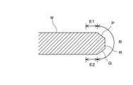
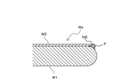
- FIG. 1A and 1B are enlarged cross-sectional views showing a peripheral portion of a wafer which is an example of a substrate. More specifically, FIG. 1A is a cross-sectional view of a so-called straight type wafer, and FIG. 1B is a cross-sectional view of a so-called round type wafer.
- the bevel portion is the outermost peripheral surface of the wafer W composed of an upper inclined portion (upper bevel portion) P, a lower inclined portion (lower bevel portion) Q, and a side portion (apex) R. (Represented by reference numeral B).
- the bevel portion is a portion having a curved cross section (indicated by reference numeral B) constituting the outermost peripheral surface of the wafer W.
- the top edge portion E1 is a region located radially inside the bevel portion B and is a flat portion located radially outside the region D in which the device is formed.
- the top edge portion E1 may include a region in which the device is formed.
- the bottom edge portion E2 is a flat portion located on the opposite side of the top edge portion E1 and radially inside the bevel portion B.
- the top edge portion E1 and the bottom edge portion E2 may be collectively referred to as a near edge portion.
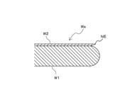
- FIG. 2A is a schematic diagram showing an example of a laminated substrate in which two wafers are bonded
- FIG. 2B is a schematic diagram showing a laminated substrate after the second wafer shown in FIG. 2A is thinned.
- the laminated substrate Ws shown in FIG. 2A is manufactured by joining the round type first wafer W1 and the second wafer W2 shown in FIG. 1B.
- a knife edge portion NE is formed on the peripheral edge portion of the second wafer W2.
- the knife edge portion NE is easily chipped due to physical contact, and may cause the laminated substrate Ws to be cracked or chipped during transportation of the laminated substrate Ws and further process processing of the laminated substrate Ws. Further, if the bonding between the first wafer W1 and the second wafer W2 is not sufficient, the second wafer W2 may be cracked or chipped during the grinding process (that is, the thinning process) of the second wafer W2. .. Even when the laminated substrate Ws is manufactured by joining the square type first wafer W1 and the second wafer W2 shown in FIG. 1A, when the second wafer W2 is thinned, a knife is formed on the peripheral edge of the second wafer W2. An edge portion is formed.
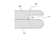
- FIG. 3A is a schematic diagram showing another example of a laminated substrate in which two wafers are bonded
- FIG. 3B is a schematic diagram showing a laminated substrate after the second wafer shown in FIG. 3A is thinned.
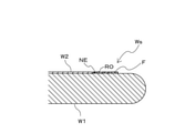
- the laminated substrate Ws shown in FIG. 3A is also manufactured by joining the round type first wafer W1 and the second wafer W2 shown in FIG. 1B, and the peripheral edge portion of the second wafer W2 is the second wafer W2. Is polished before being bonded to the first wafer W1. Therefore, a step portion S is formed on the peripheral edge portion of the second wafer W2 over the entire circumference thereof. Further, when the peripheral edge portion of the second wafer W2 is polished to form the step portion S, the roll-off portion RO may be formed on the surface of the second wafer W2 radially inside the step portion S. be.
- this roll-off portion RO can become a knife edge portion NE which is an acute-angled end portion after the second wafer W2 is thinned. Therefore, even if the peripheral edge portion of the second wafer W2 is polished in advance, it is not sufficient to suppress cracking and chipping of the laminated substrate Ws.
- a filler is applied between the first wafer W1 and the second wafer W2 of the laminated substrate Ws, and the filler is cured to effectively protect the knife edge portion NE.
- FIG. 4 is a plan view schematically showing the substrate processing apparatus according to the embodiment
- FIG. 5 is a vertical cross-sectional view schematically showing the substrate processing apparatus shown in FIG.
- the substrate processing apparatus shown in FIGS. 4 and 5 is an apparatus that applies a filler to the gaps formed between the wafers W1 and W2 of the laminated substrate Ws and further cures the filler. Note that FIG. 5 omits the illustration of the coating module 1A and the curing module 1B, which will be described later.
- the substrate processing apparatus 100 horizontally holds a laminated substrate Ws (see FIG. 2A or FIG. 3A) in which a plurality of wafers W1 and W2 are laminated in a central portion thereof, and rotates. It is provided with a rotation holding mechanism (board holding portion) 3 for causing the rotation to be held.
- FIG. 4 shows a state in which the rotation holding mechanism 3 holds the laminated substrate Ws.
- the rotation holding mechanism 3 includes a dish-shaped holding stage 4 that holds the back surface of the laminated substrate Ws by vacuum suction, a hollow shaft 5 connected to the central portion of the holding stage 4, and a motor M1 that rotates the hollow shaft 5. It is equipped with.
- the laminated substrate Ws is placed on the holding stage 4 by a hand (not shown) of the transport mechanism so that the center of the laminated substrate Ws coincides with the axis of the hollow shaft 5.
- the hollow shaft 5 is supported by a ball spline bearing (linear motion bearing) 6 so as to be vertically movable.
- a groove 4a is formed on the upper surface of the holding stage 4, and the groove 4a communicates with a communication passage 7 extending through the hollow shaft 5.
- the communication passage 7 is connected to the vacuum line 9 via a rotary joint 8 attached to the lower end of the hollow shaft 5.
- the communication passage 7 is also connected to a nitrogen gas supply line 10 for separating the treated laminated substrate Ws from the holding stage 4. By switching between these vacuum lines 9 and the nitrogen gas supply line 10, the laminated substrate Ws is vacuum-adsorbed to the upper surface of the holding stage 4 and detached.
- the hollow shaft 5 is rotated by the motor M1 via a pulley p1 connected to the hollow shaft 5, a pulley p2 attached to the rotation shaft of the motor M1, and a belt b1 hung on the pulleys p1 and p2. ..
- the rotation shaft of the motor M1 extends parallel to the hollow shaft 5. With such a configuration, the laminated substrate Ws held on the upper surface of the holding stage 4 is rotated by the motor M1.
- the ball spline bearing 6 is a bearing that allows the hollow shaft 5 to move freely in the longitudinal direction thereof.
- the ball spline bearing 6 is fixed to the cylindrical casing 12. Therefore, in the present embodiment, the hollow shaft 5 is configured to be able to operate linearly up and down with respect to the casing 12, and the hollow shaft 5 and the casing 12 rotate integrally.
- the hollow shaft 5 is connected to an air cylinder (elevating mechanism) 15, and the hollow shaft 5 and the holding stage 4 can be raised and lowered by the air cylinder 15.
- a radial bearing 18 is interposed between the casing 12 and the cylindrical casing 14 arranged concentrically on the outside thereof, and the casing 12 is rotatably supported by the bearing 18.
- the rotation holding mechanism 3 can rotate the laminated substrate Ws around its central axis Cr and raise and lower the laminated substrate Ws along the central axis Cr.
- the substrate processing apparatus 100 includes a coating joule (coating portion) 1A arranged around the laminated substrate Ws held by the rotation holding mechanism 3 and a curing module (curing portion) 1B. ing.
- the curing module 1B is located on the downstream side of the coating module 1B in the rotation direction of the laminated substrate Ws.
- the coating module 1A is a device for applying a filler to the gap between the peripheral edge portion of the first wafer W1 and the peripheral edge portion of the second wafer W2, and the curing module 1B is supplied to the laminated substrate Ws by the coating module 1A. It is a device that cures the filler.
- the filler is a thermosetting filler. Examples of such fillers include thermosetting resins.
- the coating module 1A and the curing module 1B are arranged in the processing chamber 21 partitioned by the partition wall 20, and the processing chamber 21 is separated from the outside by the partition wall 20.
- the coating module 1A, the curing module 1B, and the holding stage 4 are arranged in the processing chamber 21. That is, the laminated substrate Ws being processed is housed in the processing chamber 21.
- FIG. 5 shows a state in which the hollow shaft 5 is lowered, and shows that the holding stage 4 is in the processing position. After the filler is applied and cured, the wafer W is raised to the transfer position together with the holding stage 4 and the hollow shaft 5 by the air cylinder 15, and the wafer W is separated from the holding stage 4 at this transfer position.
- the partition wall 20 is provided with a transport port 20b for loading and unloading the laminated substrate Ws into and out of the processing chamber 21.
- the transport port 20b is formed as a notch extending horizontally. Therefore, the laminated substrate Ws gripped by the transport mechanism can cross the inside of the processing chamber 21 through the transport port 20b while maintaining a horizontal state.
- An opening 20c and a louver 40 are provided on the upper surface of the partition wall 20, and an exhaust port (not shown) is provided on the lower surface.
- the transport port 20b is closed by a shutter (not shown). Therefore, a downflow of clean air is formed inside the processing chamber 21 by exhausting air from the exhaust port by a fan mechanism (not shown). This fan mechanism functions as a pressure adjusting device that keeps the pressure in the processing chamber 21 positive. Since the laminated substrate Ws is processed in this state, the laminated substrate Ws can be processed while keeping the upper space of the processing chamber 21 clean.
- FIG. 6 is a schematic diagram showing a coating module according to an embodiment.
- the coating module 1A shown in FIG. 6 has a syringe mechanism 45 for injecting a filler into a gap between the first wafer W1 and the second wafer W2, and a horizontal moving mechanism for moving the syringe mechanism 45 close to or away from the laminated substrate Ws. (Not shown).
- the horizontal movement mechanism may be omitted.
- the position of the syringe mechanism 45 with respect to the holding stage 4 is predetermined so that the filler can be appropriately injected into the gap between the first wafer W1 and the second wafer W2.
- the syringe mechanism 45 includes a syringe body 46 having a hollow structure and a piston 48 capable of reciprocating in the syringe body 46.
- the syringe body 46 is connected to the gas supply source via the gas supply line 50.
- a gas for example, dry air or nitrogen gas
- the piston 48 advances in the syringe body 46.
- the syringe body 46 has a tip opening facing the gap between the peripheral edge portion of the first wafer W1 and the peripheral edge portion of the second wafer W2.
- the syringe body 46 is pre-filled with the filler F, and by advancing the piston 48, the gap between the peripheral edge of the first wafer W1 and the peripheral edge of the second wafer W2 is formed from the tip opening of the syringe body 46. Filler F is injected.
- a pressure regulator (for example, a pressure reducing valve) 51 and a flow rate regulator (for example, a mass flow controller) 53 are arranged in the gas supply line 50.
- a pressure regulator for example, a pressure reducing valve
- a flow rate regulator for example, a mass flow controller
- the holding stage 4 holding the laminated substrate Ws is rotated at a predetermined rotation speed.
- the syringe mechanism 45 is brought close to the laminated substrate Ws, and gas is further supplied to the syringe body 46 from the gas supply source.
- the filler F is injected into the gap between the peripheral edge portion of the first wafer W1 and the peripheral edge portion of the second wafer W2 of the rotating laminated substrate Ws.
- the filler F injected from the syringe mechanism 45 into the gap between the peripheral edge of the first wafer W1 and the peripheral edge of the second wafer W2 is too large, the filler F overflowing from the gap will be discharged from the laminated substrate Ws. There is a risk of contaminating the top and bottom surfaces. If the amount of filler F injected from the syringe mechanism 45 into the gap between the peripheral edge of the first wafer W1 and the peripheral edge of the second wafer W2 is too small, a sufficient amount of filler F is applied to the gap. May not be possible.
- the necessary and sufficient amount of the filler F is supplied to the gap between the peripheral edge portion of the first wafer W1 and the peripheral edge portion of the second wafer W2 of the rotating laminated substrate Ws.
- the flow rate of the filler F discharged from the syringe body 46 and the rotation speed of the holding stage 4 are adjusted in advance.
- FIG. 7 is a schematic diagram showing a curing module according to an embodiment.
- the curing module 1B shown in FIG. 7 is configured as an optical heating module having a lamp heater 55.
- the lamp heater 55 includes a lamp 83 and an optical device 85 that directs heat (radiant heat) from the lamp 83 to the filler F applied to the gap between the first wafer W1 and the second wafer W2.
- the optical instrument 85 is composed of, for example, a mirror and / or a lens.
- the lamp heater 55 shown in FIG. 7 is arranged above the second wafer W2 of the laminated substrate Ws, and the lamp 83 irradiates light having a wavelength of 1 ⁇ m or more from above the laminated substrate Ws via the optical device 85. ..
- the lamp 83 irradiates light having a wavelength of 1 ⁇ m or more
- the light emitted from the lamp 83 passes through the second wafer W2, so that the peripheral portion of the first wafer W1 and the peripheral portion of the second wafer W2
- the filler F applied to the gap between them can be directly heated.
- the optical heating module having the lamp 83 has high thermal efficiency and can heat and cure the filler F in a short time. Therefore, the throughput of the substrate processing apparatus 100 can be improved.
- the position of the lamp heater 55 with respect to the laminated substrate Ws is arbitrary.
- the lamp heater 55 may be arranged below the first wafer W1. In this case, the light emitted from the lamp 83 passes through the first wafer W1 and directly heats the filler F.
- the lamp heater 55 is arranged so that the lamp 83 faces the gap between the peripheral edge portion of the first wafer W1 and the peripheral edge portion of the second wafer W2. May be good. In this case, the lamp 83 heats the filler F from the side of the laminated substrate Ws. Therefore, since it is not necessary for the light emitted from the lamp 83 to pass through the first wafer W1 or the second wafer W2, any lamp can be used as the lamp 83.
- the laminated substrate Ws is first held by the holding stage 4 of the rotation holding mechanism 3 by vacuum suction. Next, the laminated substrate Ws is rotated together with the holding stage 4. Next, the filler F is applied to the gap between the peripheral edge portion of the first wafer W1 and the peripheral edge portion of the second wafer W2 of the laminated substrate Ws by the coating module 1A, and the filler F is further cured by the curing module 1B. ..
- the coating treatment and the curing treatment of the filler F are continuously performed in the same treatment chamber 21. Therefore, the substrate processing for suppressing the cracking and chipping of the laminated substrate Ws can be performed in a very short time.
- the laminated substrate Ws is carried out from the substrate processing apparatus 100, and the second wafer W2 of the laminated substrate Ws is thinned by another semiconductor manufacturing apparatus.
- FIG. 8A is a schematic view showing a filler cured in the gap between the peripheral edge portion of the first wafer and the peripheral edge portion of the second wafer of the laminated substrate shown in FIG. 2A
- FIG. 8B is a schematic view of the laminated substrate shown in FIG. 8A. It is a schematic diagram which shows the state which the 2nd wafer is thinned. As shown in FIG. 8B, even if the second wafer W2 is thinned, the second wafer W2 is covered with the filler F cured in the gap between the peripheral edge portion of the first wafer W1 and the peripheral edge portion of the second wafer W2. The knife edge portion NE formed on the peripheral portion is protected.
- the peripheral edge portion of the first wafer W1 and the peripheral edge portion of the second wafer W2 are supported by each other via the cured filler F.
- the strength of the laminated substrate Ws is increased, and it is possible to effectively suppress the occurrence of cracking and chipping of the laminated substrate Ws when the second wafer W2 is thinned.
- FIG. 9A is a schematic view showing a filler cured in the gap between the peripheral edge portion of the first wafer and the peripheral edge portion of the second wafer of the laminated substrate shown in FIG. 3A
- FIG. 9B is a schematic view of the laminated substrate shown in FIG. 9A. It is a schematic diagram which shows the state which the 2nd wafer is thinned.
- the filler F is cured in the gap between the peripheral edge portion of the first wafer W1 and the peripheral edge portion of the second wafer W2, including the step portion S and the roll-off portion RO.
- the strength of the laminated substrate Ws is increased, and it is possible to effectively suppress the occurrence of cracking and chipping of the laminated substrate Ws when the second wafer W2 is thinned.
- the filler F protects the knife edge portion NE formed on the peripheral edge portion of the second wafer W2. To. As a result, cracking and chipping of the laminated substrate Ws can be suppressed.
- the coating module 1A has a syringe mechanism 45, but the present embodiment is not limited to this example.
- the configuration of the coating module 1A is arbitrary as long as the filler F can be applied to the gap between the peripheral edge of the first wafer W1 of the laminated substrate Ws and the peripheral edge of W2 of the second wafer.
- FIG. 10 is a schematic diagram showing a coating module according to another embodiment.
- the coating module 1A shown in FIG. 10 has an injection mechanism 60 that ejects the filler F into the gap between the peripheral portion of the first wafer and the peripheral portion of the second wafer of the laminated substrate Ws instead of the syringe mechanism 45. It differs from the coating module 1A shown in FIG. 6 in that it is different from the coating module 1A shown in FIG.
- the injection mechanism 60 shown in FIG. 10 has a tubular injection machine 61 having an injection port 61a.
- the injection port 61a faces the gap between the peripheral edge portion of the first wafer and the peripheral edge portion of the second wafer of the laminated substrate Ws.
- the injection machine 61 has a filler F filled therein in advance, and is connected to the gas supply source via the gas supply line 50.
- a gas for example, dry air or nitrogen gas
- the filler F is formed in the gap between the peripheral edge of the first wafer W1 and the peripheral edge of the second wafer W2 from the injection port 61a. Is continuously ejected.
- the injection machine 61 may be a piston cylinder device.
- the gas supplied from the gas supply source to the injection machine 61 causes the piston to move forward in the cylinder, and the filler F filled in the cylinder is continuously injected from the injection port 61a.
- a pressure regulator (for example, a pressure reducing valve) 51 and a flow rate regulator (for example, a mass flow controller) 53 are arranged in the gas supply line 50.
- a pressure regulator for example, a pressure reducing valve
- a flow rate regulator for example, a mass flow controller
- the injection port is provided so that a necessary and sufficient amount of the filler F is supplied to the gap between the peripheral edge portion of the first wafer W1 and the peripheral edge portion of the second wafer W2 of the rotating laminated substrate Ws.
- the flow rate of the filler F ejected from 61a and the rotation speed of the holding stage 4 are adjusted in advance.
- FIG. 11 is a schematic diagram showing a coating module according to still another embodiment.
- the coating module 1A shown in FIG. 11 differs from the coating module 1A shown in FIG. 6 in that it has a carrier 65 for the filler F instead of the syringe mechanism 45.
- the transport mechanism 65 shown in FIG. 11 includes a tube 66 having a discharge port 66a and a filler transport member 68 connected to the discharge port 66a.
- the filler transport member 68 is a rod-shaped member extending diagonally downward from the lower end of the discharge port 66a, and the tip of the filler transport member 68 is a peripheral portion of the first wafer W1 and the second wafer W2 of the laminated substrate Ws. Close to or in contact with the gap between the edges.
- the filler transport member 68 is formed of a hydrophilic material. In one embodiment, the surface of the filler transport member 68 may be subjected to a hydrophilic treatment such as coating of a hydrophilic material.
- the filler transport member 68 has a thickness that can be inserted into the gap between the peripheral edge portion of the first wafer W1 and the peripheral edge portion of the second wafer W2, for example.
- the filler transport member 68 preferably has flexibility so as not to damage the laminated substrate Ws.
- the tube 66 has a filler F filled therein in advance, and is connected to a gas supply source via a gas supply line 50.
- a gas for example, dry air or nitrogen gas
- the filler F flows out from the discharge port 66a and flows on the surface of the filler transport member 68. Since the tip of the filler transport member 68 is close to or in contact with the gap between the peripheral edge portion of the first wafer W1 and the peripheral edge portion of the second wafer W2, the filler F is transferred to the filler transport member. It can be conveyed to the gap between the peripheral edge portion of the first wafer W1 and the peripheral edge portion of the second wafer W2 via 68.
- the tube 66 is provided so that a necessary and sufficient amount of filler F is supplied to the gap between the peripheral edge portion of the first wafer W1 and the peripheral edge portion of the second wafer W2 of the rotating laminated substrate Ws.
- the flow rate of the filler F flowing out of the filler F and the rotation speed of the holding stage 4 are adjusted in advance. According to such a configuration, the amount of the filler F supplied to the gap between the peripheral edge portion of the first wafer W1 and the peripheral edge portion of the second wafer W2 can be controlled more precisely.
- the transport mechanism 65 may have a piston cylinder device instead of the tube 66.
- the filler transport member 68 is connected to the tip opening of the cylinder of the piston cylinder device.
- the curing module 1B is configured as a light heating module having a lamp 83, but the present embodiment is not limited to this example.
- the configuration of the coating module 1B is arbitrary as long as it is possible to cure the filler F applied to the gap between the peripheral portion of the first wafer W1 of the laminated substrate Ws and the peripheral portion of W2 of the second wafer.
- FIG. 12 is a schematic diagram showing a curing module according to another embodiment.
- the curing module 1B shown in FIG. 12 is a heat gun that blows hot air toward the filler F applied to the gap between the peripheral edge portion of the first wafer W1 and the peripheral edge portion of the second wafer W2 instead of the lamp heater 55. It differs from the curing module 1B shown in FIG. 7 in that it has 87.
- the heat gun 87 shown in FIG. 12 has an injection port 87a facing the filler F applied to the gap between the peripheral edge portion of the first wafer W1 and the peripheral edge portion of the W2 of the second wafer of the laminated substrate Ws. Further, the heat gun 87 has a heater (not shown) arranged inside the heat gun 87, and a fan device (not shown) that sends the gas heated by the heater toward the injection port 87a. The heat gun 87 cures the filler F while pressing the filler F toward the center of the laminated substrate Ws by the hot air ejected from the injection port 87a.
- the filler F applied to the gap between the peripheral edge portion of the first wafer W1 and the peripheral edge portion of the second wafer W2 of the laminated substrate Ws. Can be instantly heated and cured.
- the filler F may evaporate rapidly and voids may be formed in the filler F after curing.
- the heat gun 87 is configured so that the amount of hot air blown from the injection port 87a and the temperature of the hot air can be adjusted. Therefore, the heat gun 87 can heat the filler F more slowly than the light heating of the lamp 83, and can appropriately press the filler F toward the center of the laminated substrate Ws by hot air. By this action of the heat gun 87, it is possible to effectively suppress the formation of voids in the filler F after curing.
- the present invention can be used as a substrate processing method for suppressing cracking and chipping of a laminated substrate manufactured by joining a plurality of substrates. Further, the present invention can be used for a substrate processing apparatus capable of carrying out such a substrate processing method.
Abstract
本発明は、複数の基板を接合して製造される積層基板の割れおよび欠けを抑制する基板処理方法に関する。さらに、本発明は、このような基板処理方法を実施可能な基板処理装置に関する。本方法は、第1基板(W1)と第2基板(W2)を接合して製造される積層基板(Ws)を回転させ、第1基板(W1)の周縁部と、第2基板(W2)の周縁部との間の隙間に熱硬化性を有する充填剤(F)を塗布し、この充填剤(F)を硬化させる。充填剤(F)を塗布する工程と、充填剤(F)を硬化させる工程は、同一の処理室(21)内で連続して行われる。
Description
本発明は、複数の基板を接合して製造される積層基板の割れおよび欠けを抑制する基板処理方法に関する。さらに、本発明は、このような基板処理方法を実施可能な基板処理装置に関する。
近年、半導体デバイスのさらなる高密度化および高機能化を達成するために、複数の基板を積層して3次元的に集積化する3次元実装技術の開発が進んでいる。3次元実装技術では、例えば、集積回路および電気配線が形成された第1基板のデバイス面を、同様に集積回路および電気配線が形成された第2基板のデバイス面と接合する。さらに、第1基板を第2基板に接合した後で、第2基板が研磨装置または研削装置によって薄化される。このようにして、第1基板および第2基板のデバイス面に垂直な方向に集積回路を積層することができる。
3次元実装技術では、3枚以上の基板が接合されてもよい。例えば、第1基板に接合された第2基板を簿化した後で、第3基板を第2基板に接合し、第3基板を簿化してもよい。本明細書では、互いに接合された複数の基板の形態を「積層基板」と称することがある。
通常、基板の外周面は、割れ(クラック)や欠け(チッピング)を防止するために、丸みを帯びた形状に予め研磨されている。このような丸みを帯びた外周面を有する第2基板を研削すると、その結果として第2基板には鋭角な端部が形成される。この鋭角な端部(以下、ナイフエッジ部という)は、研削された第2基板の裏面と第2基板の外周面とにより形成される。このようなナイフエッジ部は、物理的な接触により欠けやすく、積層基板の搬送時に積層基板自体が破損することがある。また、第1基板と第2基板の接合が十分でないと、第2基板が研削中に割れることもある。
そこで、本発明は、複数の基板を接合して製造される積層基板の割れおよび欠けを抑制するための基板処理方法を提供することを目的とする。
また、本発明は、上記方法を実施可能な基板処理装置を提供することを目的とする。
また、本発明は、上記方法を実施可能な基板処理装置を提供することを目的とする。
一態様では、第1基板と第2基板を接合して製造される積層基板を回転させ、前記第1基板の周縁部と、前記第2基板の周縁部との間の隙間に熱硬化性を有する充填剤を塗布し、前記充填剤を硬化させ、前記充填剤を塗布する工程と、前記充填剤を硬化させる工程は、同一の処理室内で連続して行われる、基板処理方法が提供される。
一態様では、前記充填剤を塗布する工程は、シリンジ機構を用いて前記充填剤を前記隙間に注入する工程であり、前記シリンジ機構は、前記充填剤が充填されたシリンジ本体と、前記シリンジ本体内を移動可能なピストンと、を有し、前記シリンジ本体の先端開口は、前記隙間に対向している。
一態様では、前記充填剤を塗布する工程は、射出機構を用いて前記充填剤を前記隙間に射出する工程であり、前記射出機構は、前記充填剤が充填された射出機を有し、前記射出機は、前記隙間に対向する射出口を有する。
一態様では、前記充填剤を塗布する工程は、搬送機構を用いて前記充填剤を前記隙間に搬送する工程であり、前記搬送機構は、吐出口を有し、充填剤が充填されたチューブと、前記吐出口から延びて、前記隙間に近接するか、または接触する充填剤搬送部材と、を有する。
一態様では、前記充填剤を塗布する工程は、射出機構を用いて前記充填剤を前記隙間に射出する工程であり、前記射出機構は、前記充填剤が充填された射出機を有し、前記射出機は、前記隙間に対向する射出口を有する。
一態様では、前記充填剤を塗布する工程は、搬送機構を用いて前記充填剤を前記隙間に搬送する工程であり、前記搬送機構は、吐出口を有し、充填剤が充填されたチューブと、前記吐出口から延びて、前記隙間に近接するか、または接触する充填剤搬送部材と、を有する。
一態様では、前記充填剤を硬化させる工程は、ランプヒータによって前記充填剤を硬化させる工程である。
一態様では、前記ランプヒータは、1μm以上の波長を有する光を、前記積層基板の上方または下方から前記充填剤に向けて照射させる。
一態様では、前記充填剤を硬化させる工程は、ヒートガンによって前記充填剤を硬化させる工程である。
一態様では、前記ランプヒータは、1μm以上の波長を有する光を、前記積層基板の上方または下方から前記充填剤に向けて照射させる。
一態様では、前記充填剤を硬化させる工程は、ヒートガンによって前記充填剤を硬化させる工程である。
一態様では、第1基板と第2基板を接合して製造される積層基板を保持し、回転させる基板保持部と、前記第1基板の周縁部と、前記第2基板の周縁部との間の隙間に熱硬化性を有する充填剤を塗布する塗布モジュールと、前記充填剤を硬化させる硬化モジュールと、前記基板保持部、前記塗布モジュール、および前記硬化モジュールが配置された処理室と、を備え、前記充填剤の塗布および硬化は、前記処理室内で前記積層基板を回転させながら連続して行われる、基板処理装置が提供される。
一態様では、前記塗布モジュールは、シリンジ機構を備えており、前記シリンジ機構は、前記充填剤が充填されたシリンジ本体と、前記シリンジ本体内を移動可能なピストンと、を有し、前記シリンジ本体の先端開口は、前記隙間に対向している。
一態様では、前記塗布モジュールは、射出機構を備えており、前記射出機構は、前記充填剤が充填された射出機を有し、前記射出機は、前記隙間に対向する射出口を有する。
一態様では、前記塗布モジュールは、搬送機構を備えており、前記搬送機構は、吐出口を有し、充填剤が充填されたチューブと、前記吐出口から延びて、前記隙間に近接するか、または接触する充填剤搬送部材と、を有する。
一態様では、前記塗布モジュールは、射出機構を備えており、前記射出機構は、前記充填剤が充填された射出機を有し、前記射出機は、前記隙間に対向する射出口を有する。
一態様では、前記塗布モジュールは、搬送機構を備えており、前記搬送機構は、吐出口を有し、充填剤が充填されたチューブと、前記吐出口から延びて、前記隙間に近接するか、または接触する充填剤搬送部材と、を有する。
一態様では、前記硬化モジュールは、ランプヒータを備えており、前記ランプヒータは、ランプと、前記ランプからの熱を、前記隙間に塗布された充填剤に向ける光学機器と、を有している。
一態様では、前記ランプは、1μm以上の波長を有する光を発するように構成されており、前記ランプヒータは、前記積層基板の上方または下方に配置される。
一態様では、前記硬化モジュールは、前記充填剤に向けて熱風を吹き付けるヒートガンを備える。
一態様では、前記ランプは、1μm以上の波長を有する光を発するように構成されており、前記ランプヒータは、前記積層基板の上方または下方に配置される。
一態様では、前記硬化モジュールは、前記充填剤に向けて熱風を吹き付けるヒートガンを備える。
本発明によれば、第1基板の周縁部と第2基板の周縁部との間の隙間で硬化された充填剤によって第2基板の周縁部に形成されたナイフエッジ部が保護される。その結果、積層基板の割れおよび欠けを抑制することができる。さらに、第1基板の周縁部と第2基板の周縁部が硬化された充填剤を介して互いに支持される。その結果、積層基板の強度が増加し、第2基板を薄化する際に、積層基板の割れおよび欠けが発生することを効果的に抑制することができる。
以下、本発明の実施形態について図面を参照して説明する。
図1Aおよび図1Bは、基板の一例であるウエハの周縁部を示す拡大断面図である。より詳しくは、図1Aはいわゆるストレート型のウエハの断面図であり、図1Bはいわゆるラウンド型のウエハの断面図である。図1AのウエハWにおいて、ベベル部は、上側傾斜部(上側ベベル部)P、下側傾斜部(下側ベベル部)Q、および側部(アペックス)Rから構成されるウエハWの最外周面(符号Bで示す)である。
図1Aおよび図1Bは、基板の一例であるウエハの周縁部を示す拡大断面図である。より詳しくは、図1Aはいわゆるストレート型のウエハの断面図であり、図1Bはいわゆるラウンド型のウエハの断面図である。図1AのウエハWにおいて、ベベル部は、上側傾斜部(上側ベベル部)P、下側傾斜部(下側ベベル部)Q、および側部(アペックス)Rから構成されるウエハWの最外周面(符号Bで示す)である。
図1BのウエハWにおいては、ベベル部は、ウエハWの最外周面を構成する、湾曲した断面を有する部分(符号Bで示す)である。トップエッジ部E1は、ベベル部Bよりも半径方向内側に位置する領域であって、かつデバイスが形成される領域Dよりも半径方向外側に位置する平坦部である。トップエッジ部E1は、デバイスが形成された領域を含むこともある。ボトムエッジ部E2は、トップエッジ部E1とは反対側に位置し、ベベル部Bよりも半径方向内側に位置する平坦部である。これらトップエッジ部E1およびボトムエッジ部E2は、総称してニアエッジ部と呼ばれることもある。
図2Aは、2枚のウエハを接合した積層基板の一例を示す模式図であり、図2Bは、図2Aに示す第2ウエハを薄化した後の積層基板を示す模式図である。図2Aに示す積層基板Wsは、図1Bに示すラウンド型の第1ウエハW1と第2ウエハW2とを接合することにより製造される。
図2Bに示すように、第2ウエハW2を薄化すると、第2ウエハW2の周縁部にナイフエッジ部NEが形成される。このナイフエッジ部NEは、物理的な接触により欠けやすく、積層基板Wsの搬送時、および積層基板Wsのさらなるプロセス処理時に積層基板Wsが割れたり、欠けたりさせる要因となることがある。また、第1ウエハW1と第2ウエハW2の接合が十分でないと、第2ウエハW2の研削プロセス(すなわち、薄化プロセス)中に、該第2ウエハW2が割れたり、欠けたりすることもある。積層基板Wsが図1Aに示すスクエア型の第1ウエハW1と第2ウエハW2とを接合することにより製造される場合も、第2ウエハW2を薄化すると、第2ウエハW2の周縁部にナイフエッジ部が形成される。
図3Aは、2枚のウエハを接合した積層基板の他の例を示す模式図であり、図3Bは、図3Aに示す第2ウエハを薄化した後の積層基板を示す模式図である。図3Aに示す積層基板Wsも、図1Bに示すラウンド型の第1ウエハW1と第2ウエハW2とを接合することにより製造されるが、第2ウエハW2の周縁部は、該第2ウエハW2を第1ウエハW1に接合する前に研磨されている。そのため、第2ウエハW2の周縁部には、その全周にわたって、段差部Sが形成されている。さらに、段差部Sを形成するために第2ウエハW2の周縁部を研磨する際に、該段差部Sよりも半径方向内側の第2ウエハW2の表面にロールオフ部ROが形成されることがある。
図3Bに示すように、このロールオフ部ROは、第2ウエハW2を薄化した後で鋭角な端部であるナイフエッジ部NEとなりうる。そのため、第2ウエハW2の周縁部を予め研磨しておいても、積層基板Wsの割れおよび欠けを抑制するには十分ではない。
そこで、本実施形態では、積層基板Wsの第1ウエハW1と第2ウエハW2との間に充填剤を塗布し、この充填剤を硬化させることで、ナイフエッジ部NEを効果的に保護する。
図4は、一実施形態に係る基板処理装置を模式的に示す平面図であり、図5は、図4に示す基板処理装置を模式的に示す縦断面図である。図4および図5に示す基板処理装置は、積層基板WsのウエハW1,W2の間に形成された隙間に充填剤を塗布し、さらに硬化させる装置である。なお、図5は、後述する塗布モジュール1Aおよび硬化モジュール1Bの図示を省略している。
図4および図5に示すように、この基板処理装置100は、その中央部に、複数のウエハW1,W2が積層された積層基板Ws(図2Aまたは図3A参照)を水平に保持し、回転させる回転保持機構(基板保持部)3を備えている。図4においては、回転保持機構3が積層基板Wsを保持している状態を示している。回転保持機構3は、積層基板Wsの裏面を真空吸着により保持する皿状の保持ステージ4と、保持ステージ4の中央部に連結された中空シャフト5と、この中空シャフト5を回転させるモータM1とを備えている。積層基板Wsは、搬送機構のハンド(図示せず)により、積層基板Wsの中心が中空シャフト5の軸心と一致するように保持ステージ4の上に載置される。
中空シャフト5は、ボールスプライン軸受(直動軸受)6によって上下動自在に支持されている。保持ステージ4の上面には溝4aが形成されており、この溝4aは、中空シャフト5を通って延びる連通路7に連通している。連通路7は中空シャフト5の下端に取り付けられたロータリジョイント8を介して真空ライン9に接続されている。連通路7は、処理後の積層基板Wsを保持ステージ4から離脱させるための窒素ガス供給ライン10にも接続されている。これらの真空ライン9と窒素ガス供給ライン10を切り替えることによって、積層基板Wsを保持ステージ4の上面に真空吸着し、離脱させる。
中空シャフト5は、この中空シャフト5に連結されたプーリーp1と、モータM1の回転軸に取り付けられたプーリーp2と、これらプーリーp1,p2に掛けられたベルトb1を介してモータM1によって回転される。モータM1の回転軸は中空シャフト5と平行に延びている。このような構成により、保持ステージ4の上面に保持された積層基板Wsは、モータM1によって回転される。
ボールスプライン軸受6は、中空シャフト5がその長手方向へ自由に移動することを許容する軸受である。ボールスプライン軸受6は円筒状のケーシング12に固定されている。したがって、本実施形態においては、中空シャフト5は、ケーシング12に対して上下に直線動作ができるように構成されており、中空シャフト5とケーシング12は一体に回転する。中空シャフト5は、エアシリンダ(昇降機構)15に連結されており、エアシリンダ15によって中空シャフト5および保持ステージ4が上昇および下降できるようになっている。
ケーシング12と、その外側に同心上に配置された円筒状のケーシング14との間にはラジアル軸受18が介装されており、ケーシング12は軸受18によって回転自在に支持されている。このような構成により、回転保持機構3は、積層基板Wsをその中心軸Crまわりに回転させ、かつ積層基板Wsを中心軸Crに沿って上昇下降させることができる。
図4に示すように、基板処理装置100は、回転保持機構3に保持された積層基板Wsの周囲に配置された塗布ジュール(塗布部)1Aと、硬化モジュール(硬化部)1Bと、と備えている。硬化モジュール1Bは、積層基板Wsの回転方向において塗布モジュール1Bの下流側に位置している。
塗布モジュール1Aは、第1ウエハW1の周縁部と第2ウエハW2の周縁部との間の隙間に充填剤を塗布する装置であり、硬化モジュール1Bは、塗布モジュール1Aによって積層基板Wsに供給された充填剤を硬化させる装置である。本実施形態において、充填剤は、熱硬化性を有する充填剤である。このような充填剤の例はとしては、熱硬化性の樹脂が挙げられる。
塗布モジュール1Aと硬化モジュール1Bとは、隔壁20によって仕切られた処理室21内に配置されており、処理室21は、隔壁20によって外部から隔離されている。塗布モジュール1A、硬化モジュール1B、および保持ステージ4は処理室21内に配置されている。すなわち、処理中の積層基板Wsは、処理室内21に収容される。
中空シャフト5がケーシング12に対して昇降した時にボールスプライン軸受6やラジアル軸受18などの機構を処理室21から隔離するために、図5に示すように、中空シャフト5とケーシング12の上端とは上下に伸縮可能なベローズ19で接続されている。図5は中空シャフト5が下降している状態を示し、保持ステージ4が処理位置にあることを示している。充填剤の塗布および硬化処理後には、エアシリンダ15によりウエハWを保持ステージ4および中空シャフト5とともに搬送位置まで上昇させ、この搬送位置でウエハWを保持ステージ4から離脱させる。
隔壁20は、積層基板Wsを処理室21に搬入および搬出するための搬送口20bを備えている。搬送口20bは、水平に延びる切り欠きとして形成されている。したがって、搬送機構に把持された積層基板Wsは、水平な状態を保ちながら、搬送口20bを通って処理室21内を横切ることが可能となっている。隔壁20の上面には開口20cおよびルーバー40が設けられ、下面には排気口(図示せず)が設けられている。充填剤の塗布および硬化処理時は、搬送口20bは図示しないシャッターで閉じられるようになっている。したがって、排気口から図示しないファン機構により排気をすることで処理室21の内部には清浄空気のダウンフローが形成されるようになっている。このファン機構は、処理室21内の圧力を陽圧に保つ圧力調整装置として機能する。この状態において積層基板Wsが処理されるので、処理室21の上部空間を清浄に保ちながら積層基板Wsの処理をすることができる。
図6は、一実施形態にかかる塗布モジュールを示す模式図である。図6に示す塗布モジュール1Aは、第1ウエハW1と第2ウエハW2との間の隙間に充填剤を注入するシリンジ機構45と、シリンジ機構45を積層基板Wsに近接または離間させる水平移動機構(図示せず)を有している。一実施形態では、水平移動機構を省略してもよい。この場合、充填剤が第1ウエハW1と第2ウエハW2との間の隙間に適切に注入可能なように、保持ステージ4に対するシリンジ機構45の位置が予め決定されている。
シリンジ機構45は、中空構造を有するシリンジ本体46と、シリンジ本体46内を往復動可能なピストン48とを備えている。シリンジ本体46は、気体供給ライン50を介して気体供給源に接続されている。気体供給源から気体(例えば、ドライエアーまたは窒素ガス)をシリンジ本体46に供給すると、ピストン48がシリンジ本体46内を前進する。シリンジ本体46は、第1ウエハW1の周縁部と第2ウエハW2の周縁部との間の隙間に対向する先端開口を有している。シリンジ本体46には、充填剤Fが予め充填されており、ピストン48の前進によって、シリンジ本体46の先端開口から第1ウエハW1の周縁部と第2ウエハW2の周縁部との間の隙間に充填剤Fが注入される。
気体供給ライン50には、圧力調整装置(例えば、減圧弁)51と、流量調整器(例えば、マスフローコントローラ)53とが配置されている。気体供給源からシリンジ本体46に供給される気体の圧力および流量を調整することで、シリンジ本体46から吐出する充填剤Fの流量を調整することができる。
第1ウエハW1と第2ウエハW2との間の隙間に充填剤Fを塗布する際には、最初に、積層基板Wsが保持された保持ステージ4を所定の回転速度で回転させる。次いで、シリンジ機構45を積層基板Wsに近接させ、さらに、気体供給源から気体をシリンジ本体46に供給する。この動作によって、回転する積層基板Wsの第1ウエハW1の周縁部と第2ウエハW2の周縁部との間の隙間に充填剤Fが注入される。
第1ウエハW1の周縁部と第2ウエハW2の周縁部との間の隙間にシリンジ機構45から注入される充填剤Fの量が多すぎると、隙間からあふれた充填剤Fが積層基板Wsの上面および下面を汚染するおそれがある。第1ウエハW1の周縁部と第2ウエハW2の周縁部との間の隙間にシリンジ機構45から注入される充填剤Fの量が少なすぎると、該隙間に十分な量の充填剤Fを塗布することができないおそれがある。そのため、本実施形態では、回転する積層基板Wsの第1ウエハW1の周縁部と第2ウエハW2の周縁部との間の隙間に、必要十分な量の充填剤Fが供給されるように、シリンジ本体46から吐出される充填剤Fの流量、および保持ステージ4の回転速度が予め調整されている。
図7は、一実施形態に係る硬化モジュールを示す模式図である。図7に示す硬化モジュール1Bは、ランプヒータ55を有する光加熱モジュールとして構成されている。ランプヒータ55は、ランプ83と、ランプ83からの熱(輻射熱)を、第1ウエハW1と第2ウエハW2との間の隙間に塗布された充填剤Fに向ける光学機器85と、を備えている。図示はしないが、光学機器85は、例えば、ミラーおよび/またはレンズなどから構成される。
図7に示すランプヒータ55は、積層基板Wsの第2ウエハW2の上方に配置されており、ランプ83は、波長が1μm以上の光を光学機器85を介して積層基板Wsの上方から照射する。ランプ83が1μm以上の波長を有する光を照射する場合、ランプ83から照射された光は、第2ウエハW2を透過するので、第1ウエハW1の周縁部と第2ウエハW2の周縁部との間の隙間に塗布された充填剤Fを直接加熱することができる。ランプ83を有する光加熱モジュールは、熱効率が高く、短時間で充填剤Fを加熱し、硬化させることができる。したがって、基板処理装置100のスループットを向上させることができる。
積層基板Wsに対するランプヒータ55の位置は任意である。例えば、図7の一点鎖線で示されるように、ランプヒータ55を、第1ウエハW1の下方に配置してもよい。この場合、ランプ83から照射された光は第1ウエハW1を透過して、充填剤Fを直接加熱する。あるいは、図7の二点鎖線で示されるように、ランプ83が第1ウエハW1の周縁部と第2ウエハW2の周縁部との間の隙間に対向するように、ランプヒータ55を配置してもよい。この場合、ランプ83は、積層基板Wsの側方から充填剤Fを加熱する。したがって、ランプ83から照射された光が第1ウエハW1または第2ウエハW2を透過する必要がないので、ランプ83として任意のランプを用いることができる。
このように構成された基板処理装置100では、最初に、積層基板Wsが回転保持機構3の保持ステージ4に真空吸着により保持される。次いで、積層基板Wsが保持ステージ4とともに回転される。次いで、塗布モジュール1Aにより、積層基板Wsの第1ウエハW1の周縁部と第2ウエハW2の周縁部の隙間に充填剤Fが塗布され、さらに、硬化モジュール1Bにより、充填剤Fが硬化される。充填剤Fの塗布処理および硬化処理は、同一の処理室21内で連続して行われる。したがって、積層基板Wsの割れおよび欠けを抑制するための基板処理を非常に短時間で行うことができる。
その後、積層基板Wsは、基板処理装置100から搬出され、他の半導体製造装置で積層基板Wsの第2ウエハW2が薄化される。
図8Aは、図2Aに示す積層基板の第1ウエハの周縁部と第2ウエハの周縁部の隙間で硬化された充填剤を示す模式図であり、図8Bは、図8Aに示す積層基板の第2ウエハが薄化された状態を示す模式図である。図8Bに示すように、第2ウエハW2を薄化しても、第1ウエハW1の周縁部と第2ウエハW2の周縁部との間の隙間で硬化された充填剤Fによって第2ウエハW2の周縁部に形成されたナイフエッジ部NEが保護される。その結果、積層基板Wsの割れおよび欠けを抑制することができる。さらに、図8Aに示すように、第1ウエハW1の周縁部と第2ウエハW2の周縁部が硬化された充填剤Fを介して互いに支持される。その結果、積層基板Wsの強度が増加し、第2ウエハW2を薄化する際に、積層基板Wsの割れおよび欠けが発生することを効果的に抑制することができる。
図9Aは、図3Aに示す積層基板の第1ウエハの周縁部と第2ウエハの周縁部の隙間で硬化された充填剤を示す模式図であり、図9Bは、図9Aに示す積層基板の第2ウエハが薄化された状態を示す模式図である。図9Aに示すように、充填剤Fは、段差部Sおよびロールオフ部ROを含む、第1ウエハW1の周縁部と第2ウエハW2の周縁部との間の隙間で硬化されている。そのため、積層基板Wsの強度が増加し、第2ウエハW2を薄化する際に、積層基板Wsの割れおよび欠けが発生することを効果的に抑制することができる。さらに、図9Bに示すように、ロールオフ部ROに達するまで第2ウエハW2が薄化される場合でも、充填剤Fによって第2ウエハW2の周縁部に形成されたナイフエッジ部NEが保護される。その結果、積層基板Wsの割れおよび欠けを抑制することができる。
図4乃至図7を参照して説明された実施形態では、塗布モジュール1Aはシリンジ機構45を有しているが、本実施形態はこの例に限定されない。塗布モジュール1Aの構成は、積層基板Wsの第1ウエハW1の周縁部と第2ウエハのW2周縁部との間の隙間に充填剤Fを塗布できる限り任意である。
図10は、他の実施形態に係る塗布モジュールを示す模式図である。図10に示す塗布モジュール1Aは、シリンジ機構45に代えて、充填剤Fを積層基板Wsの第1ウエハの周縁部と第2ウエハの周縁部との間の隙間に射出する射出機構60を有する点で図6に示す塗布モジュール1Aと異なる。
図10に示す射出機構60は、射出口61aを有するチューブ状の射出機61を有する。射出口61aは、積層基板Wsの第1ウエハの周縁部と第2ウエハの周縁部との間の隙間に対向している。射出機61は、その内部に充填された充填剤Fを予め有しており、気体供給ライン50を介して気体供給源に接続されている。気体供給源から気体(例えば、ドライエアーまたは窒素ガス)を射出機61に供給すると、射出口61aから第1ウエハW1の周縁部と第2ウエハW2の周縁部との間の隙間に充填剤Fが連続的に射出される。
図示はしないが、射出機61は、ピストンシリンダ装置であってもよい。この場合、気体供給源から射出機61に供給された気体によって、ピストンがシリンダ内を前進し、該シリンダに充填された充填剤Fを射出口61aから連続的に射出する。
気体供給ライン50には、圧力調整装置(例えば、減圧弁)51と、流量調整器(例えば、マスフローコントローラ)53とが配置されている。気体供給源から射出機61に供給される気体の圧力および流量を調整することで、射出口61aから射出される充填剤Fの流量を調整することができる。本実施形態でも、回転する積層基板Wsの第1ウエハW1の周縁部と第2ウエハW2の周縁部との間の隙間に、必要十分な量の充填剤Fが供給されるように、射出口61aから射出される充填剤Fの流量、および保持ステージ4の回転速度が予め調整されている。
図11は、さらに他の実施形態に係る塗布モジュールを示す模式図である。図11に示す塗布モジュール1Aは、シリンジ機構45に代えて、充填剤Fの搬送機構65を有する点で図6に示す塗布モジュール1Aと異なる。
図11に示す搬送機構65は、吐出口66aを有するチューブ66と、吐出口66aに連結された充填剤搬送部材68と、を備えている。充填剤搬送部材68は、吐出口66aの下端部から斜め下方に延びる棒状の部材であり、充填剤搬送部材68の先端は、積層基板Wsの第1ウエハW1の周縁部と第2ウエハW2の周縁部との間の隙間に近接するか、または接触する。充填剤搬送部材68は、親水性を有する材料から形成される。一実施形態では、充填剤搬送部材68の表面に、親水性を有する材料のコーティングなどの親水性処理を施してもよい。充填剤搬送部材68は、例えば、第1ウエハW1の周縁部と第2ウエハW2の周縁部との間の隙間に挿入可能な太さを有する。充填剤搬送部材68は、積層基板Wsを傷つけないように可撓性を有しているのが好ましい。
チューブ66は、その内部に充填された充填剤Fを予め有しており、気体供給ライン50を介して気体供給源に接続されている。気体供給源から気体(例えば、ドライエアーまたは窒素ガス)をチューブ66に供給すると、充填剤Fが吐出口66aから流出して、充填剤搬送部材68の表面上を流れる。充填剤搬送部材68の先端は、第1ウエハW1の周縁部と第2ウエハW2の周縁部との間の隙間に近接するか、または接触しているので、充填剤Fを、充填剤搬送部材68を介して第1ウエハW1の周縁部と第2ウエハW2の周縁部との間の隙間に搬送することができる。本実施形態でも、回転する積層基板Wsの第1ウエハW1の周縁部と第2ウエハW2の周縁部との間の隙間に、必要十分な量の充填剤Fが供給されるように、チューブ66から流出される充填剤Fの流量、および保持ステージ4の回転速度が予め調整されている。このような構成によれば、第1ウエハW1の周縁部と第2ウエハW2の周縁部との間の隙間に供給される充填剤Fの量をより精密に制御することができる。
図示はしないが、搬送機構65は、チューブ66に代えて、ピストンシリンダ装置を有していてもよい。この場合、充填剤搬送部材68は、ピストンシリンダ装置のシリンダの先端開口に連結される。気体を気体供給源からピストンシリンダ装置に供給すると、ピストンがシリンダ内を前進し、該シリンダに充填された充填剤Fをシリンダの先端開口から充填剤搬送部材68に供給する。
図4乃至図7を参照して説明された実施形態では、硬化モジュール1Bはランプ83を有する光加熱モジュールとして構成されているが、本実施形態はこの例に限定されない。塗布モジュール1Bの構成は、積層基板Wsの第1ウエハW1の周縁部と第2ウエハのW2周縁部の隙間に塗布された充填剤Fを硬化させることが可能である限り任意である。
図12は、他の実施形態に係る硬化モジュールを示す模式図である。図12に示す硬化モジュール1Bは、ランプヒータ55に代えて、第1ウエハW1の周縁部と第2ウエハW2の周縁部との間の隙間に塗布された充填剤Fに向けて熱風を吹き付けるヒートガン87を有している点で図7に示す硬化モジュール1Bと異なる。
図12に示すヒートガン87は、積層基板Wsの第1ウエハW1の周縁部と第2ウエハのW2周縁部の隙間に塗布された充填剤Fに対向する射出口87aを有している。さらに、ヒートガン87は、その内部に配置されたヒータ(図示せず)と、ヒータにより加熱された気体を射出口87aに向けて送るファン装置(図示せず)などを有している。ヒートガン87は、その射出口87aから射出された熱風によって、充填剤Fを積層基板Wsの中心に向かって押し付けつつ、充填剤Fを硬化させる。
図7に示すように、硬化モジュール1Bが光加熱モジュールである場合は、積層基板Wsの第1ウエハW1の周縁部と第2ウエハのW2周縁部との間の隙間に塗布された充填剤Fを瞬時に加熱及び硬化させることができる。しかしながら、充填剤Fの硬化速度が速すぎると、充填剤Fが急激に蒸発して、硬化後の充填剤F内に空隙が生じてしまうことがある。ヒートガン87は、射出口87aから吹き出す熱風の量、および熱風の温度を調整できるように構成されている。したがって、ヒートガン87は、ランプ83の光加熱よりもゆっくりと充填剤Fを加熱することができ、かつ熱風によって充填剤Fを積層基板Wsの中心に向かって適切に押し付けることができる。ヒートガン87のこの作用によって、硬化後の充填剤F内に空隙が生じてしまうことを効果的に抑制できる。
上述した実施形態は、本発明が属する技術分野における通常の知識を有する者が本発明を実施できることを目的として記載されたものである。上記実施形態の種々の変形例は、当業者であれば当然になしうることであり、本発明の技術的思想は他の実施形態にも適用しうる。したがって、本発明は、記載された実施形態に限定されることはなく、特許請求の範囲によって定義される技術的思想に従った最も広い範囲に解釈されるものである。
本発明は、複数の基板を接合して製造される積層基板の割れおよび欠けを抑制する基板処理方法に利用可能である。さらに、本発明は、このような基板処理方法を実施可能な基板処理装置に利用可能である。
1A 塗布モジュール
1B 硬化モジュール
3 回転保持機構(基板保持部)
4 保持ステージ
20 隔壁
21 処理室
45 シリンジ機構
46 シリンジ本体
48 ピストン
50 気体供給ライン
51 圧力調整装置
53 流量調整装置
55 ランプヒータ
60 射出機構
61 射出機
65 搬送機構
66 チューブ
68 充填剤搬送部材
83 ランプ
85 光学機器
87 ヒートガン
100 基板処理装置
1B 硬化モジュール
3 回転保持機構(基板保持部)
4 保持ステージ
20 隔壁
21 処理室
45 シリンジ機構
46 シリンジ本体
48 ピストン
50 気体供給ライン
51 圧力調整装置
53 流量調整装置
55 ランプヒータ
60 射出機構
61 射出機
65 搬送機構
66 チューブ
68 充填剤搬送部材
83 ランプ
85 光学機器
87 ヒートガン
100 基板処理装置
Claims (14)
- 第1基板と第2基板を接合して製造される積層基板を回転させ、
前記第1基板の周縁部と、前記第2基板の周縁部との間の隙間に熱硬化性を有する充填剤を塗布し、
前記充填剤を硬化させ、
前記充填剤を塗布する工程と、前記充填剤を硬化させる工程は、同一の処理室内で連続して行われる、基板処理方法。 - 前記充填剤を塗布する工程は、シリンジ機構を用いて前記充填剤を前記隙間に注入する工程であり、
前記シリンジ機構は、
前記充填剤が充填されたシリンジ本体と、
前記シリンジ本体内を移動可能なピストンと、を有し、
前記シリンジ本体の先端開口は、前記隙間に対向している、請求項1に記載の基板処理方法。 - 前記充填剤を塗布する工程は、射出機構を用いて前記充填剤を前記隙間に射出する工程であり、
前記射出機構は、前記充填剤が充填された射出機を有し、
前記射出機は、前記隙間に対向する射出口を有する、請求項1に記載の基板処理方法。 - 前記充填剤を塗布する工程は、搬送機構を用いて前記充填剤を前記隙間に搬送する工程であり、
前記搬送機構は、
吐出口を有し、充填剤が充填されたチューブと、
前記吐出口から延びて、前記隙間に近接するか、または接触する充填剤搬送部材と、を有する、請求項1に記載の基板処理方法。 - 前記充填剤を硬化させる工程は、ランプヒータによって前記充填剤を硬化させる工程である、請求項1乃至4のいずれか一項に記載の基板処理方法。
- 前記ランプヒータは、1μm以上の波長を有する光を、前記積層基板の上方または下方から前記充填剤に向けて照射させる、請求項5に記載の基板処理方法。
- 前記充填剤を硬化させる工程は、ヒートガンによって前記充填剤を硬化させる工程である、請求項1乃至4のいずれか一項に記載の基板処理方法。
- 第1基板と第2基板を接合して製造される積層基板を保持し、回転させる基板保持部と、
前記第1基板の周縁部と、前記第2基板の周縁部との間の隙間に熱硬化性を有する充填剤を塗布する塗布モジュールと、
前記充填剤を硬化させる硬化モジュールと、
前記基板保持部、前記塗布モジュール、および前記硬化モジュールが配置された処理室と、を備え、
前記充填剤の塗布および硬化は、前記処理室内で前記積層基板を回転させながら連続して行われる、基板処理装置。 - 前記塗布モジュールは、シリンジ機構を備えており、
前記シリンジ機構は、
前記充填剤が充填されたシリンジ本体と、
前記シリンジ本体内を移動可能なピストンと、を有し、
前記シリンジ本体の先端開口は、前記隙間に対向している、請求項8に記載の基板処理装置。 - 前記塗布モジュールは、射出機構を備えており、
前記射出機構は、前記充填剤が充填された射出機を有し、
前記射出機は、前記隙間に対向する射出口を有する、請求項8に記載の基板処理装置。 - 前記塗布モジュールは、搬送機構を備えており、
前記搬送機構は、
吐出口を有し、充填剤が充填されたチューブと、
前記吐出口から延びて、前記隙間に近接するか、または接触する充填剤搬送部材と、を有する、請求項8に記載の基板処理装置。 - 前記硬化モジュールは、ランプヒータを備えており、
前記ランプヒータは、
ランプと、
前記ランプからの熱を、前記隙間に塗布された充填剤に向ける光学機器と、を有している、請求項8乃至11のいずれか一項に記載の基板処理装置。 - 前記ランプは、1μm以上の波長を有する光を発するように構成されており、
前記ランプヒータは、前記積層基板の上方または下方に配置される、請求項12に記載の基板処理装置。 - 前記硬化モジュールは、前記充填剤に向けて熱風を吹き付けるヒートガンを備える、請求項8乃至11のいずれか一項に記載の基板処理装置。
Priority Applications (4)
| Application Number | Priority Date | Filing Date | Title |
|---|---|---|---|
| EP21860952.7A EP4207246A1 (en) | 2020-08-27 | 2021-06-25 | Substrate processing method and substrate processing device |
| KR1020237009330A KR20230054415A (ko) | 2020-08-27 | 2021-06-25 | 기판 처리 방법 및 기판 처리 장치 |
| CN202180052111.5A CN115885367A (zh) | 2020-08-27 | 2021-06-25 | 基板处理方法及基板处理装置 |
| US18/041,256 US20230326757A1 (en) | 2020-08-27 | 2021-06-25 | Substrate processing method and substrate processing apparatus |
Applications Claiming Priority (2)
| Application Number | Priority Date | Filing Date | Title |
|---|---|---|---|
| JP2020143517A JP2022038834A (ja) | 2020-08-27 | 2020-08-27 | 基板処理方法、および基板処理装置 |
| JP2020-143517 | 2020-08-27 |
Publications (1)
| Publication Number | Publication Date |
|---|---|
| WO2022044522A1 true WO2022044522A1 (ja) | 2022-03-03 |
Family
ID=80354907
Family Applications (1)
| Application Number | Title | Priority Date | Filing Date |
|---|---|---|---|
| PCT/JP2021/024080 WO2022044522A1 (ja) | 2020-08-27 | 2021-06-25 | 基板処理方法、および基板処理装置 |
Country Status (7)
| Country | Link |
|---|---|
| US (1) | US20230326757A1 (ja) |
| EP (1) | EP4207246A1 (ja) |
| JP (1) | JP2022038834A (ja) |
| KR (1) | KR20230054415A (ja) |
| CN (1) | CN115885367A (ja) |
| TW (1) | TW202226336A (ja) |
| WO (1) | WO2022044522A1 (ja) |
Families Citing this family (3)
| Publication number | Priority date | Publication date | Assignee | Title |
|---|---|---|---|---|
| JP2024010749A (ja) * | 2022-07-13 | 2024-01-25 | 株式会社荏原製作所 | 基板保持装置、基板製造装置、および基板製造方法 |
| JP2024010745A (ja) * | 2022-07-13 | 2024-01-25 | 株式会社荏原製作所 | 基板製造方法および基板製造装置 |
| JP2024022110A (ja) * | 2022-08-05 | 2024-02-16 | 株式会社荏原製作所 | 充填剤塗布装置 |
Citations (3)
| Publication number | Priority date | Publication date | Assignee | Title |
|---|---|---|---|---|
| JP2006352078A (ja) * | 2005-05-16 | 2006-12-28 | Fuji Electric Holdings Co Ltd | 半導体装置の製造方法 |
| JP2014063955A (ja) | 2012-09-24 | 2014-04-10 | Ebara Corp | 研磨方法 |
| JP2014167966A (ja) * | 2013-02-28 | 2014-09-11 | Toshiba Corp | 半導体装置の製造方法及び製造装置 |
-
2020
- 2020-08-27 JP JP2020143517A patent/JP2022038834A/ja active Pending
-
2021
- 2021-06-25 KR KR1020237009330A patent/KR20230054415A/ko unknown
- 2021-06-25 WO PCT/JP2021/024080 patent/WO2022044522A1/ja unknown
- 2021-06-25 EP EP21860952.7A patent/EP4207246A1/en active Pending
- 2021-06-25 CN CN202180052111.5A patent/CN115885367A/zh active Pending
- 2021-06-25 US US18/041,256 patent/US20230326757A1/en active Pending
- 2021-08-24 TW TW110131224A patent/TW202226336A/zh unknown
Patent Citations (3)
| Publication number | Priority date | Publication date | Assignee | Title |
|---|---|---|---|---|
| JP2006352078A (ja) * | 2005-05-16 | 2006-12-28 | Fuji Electric Holdings Co Ltd | 半導体装置の製造方法 |
| JP2014063955A (ja) | 2012-09-24 | 2014-04-10 | Ebara Corp | 研磨方法 |
| JP2014167966A (ja) * | 2013-02-28 | 2014-09-11 | Toshiba Corp | 半導体装置の製造方法及び製造装置 |
Also Published As
| Publication number | Publication date |
|---|---|
| US20230326757A1 (en) | 2023-10-12 |
| JP2022038834A (ja) | 2022-03-10 |
| KR20230054415A (ko) | 2023-04-24 |
| TW202226336A (zh) | 2022-07-01 |
| EP4207246A1 (en) | 2023-07-05 |
| CN115885367A (zh) | 2023-03-31 |
Similar Documents
| Publication | Publication Date | Title |
|---|---|---|
| WO2022044522A1 (ja) | 基板処理方法、および基板処理装置 | |
| JP7109537B2 (ja) | 基板処理システム及び基板処理方法 | |
| JP6775880B2 (ja) | ウェーハの加工方法 | |
| JP6158721B2 (ja) | 洗浄装置、剥離システム、洗浄方法、プログラム及びコンピュータ記憶媒体 | |
| JP7058737B2 (ja) | 基板処理システム及び基板処理方法 | |
| JP6277021B2 (ja) | ウエーハ処理装置及びウエーハの処理方法 | |
| TW202105501A (zh) | 基板處理方法及基板處理裝置 | |
| JP2021106197A (ja) | 基板処理装置及び基板処理方法 | |
| KR101025192B1 (ko) | 기판처리장치 | |
| JP2022017700A (ja) | 基板処理方法、および基板処理装置 | |
| JP2005064234A (ja) | プラズマエッチング方法及びプラズマエッチング装置 | |
| WO2023042547A1 (ja) | 基板処理装置、および基板処理方法 | |
| JP2022041495A (ja) | 保護部材形成装置 | |
| US10658204B2 (en) | Spin chuck with concentrated center and radial heating | |
| JP2020061494A (ja) | ウェーハの加工方法 | |
| JP2023042561A (ja) | 基板処理装置、および基板処理方法 | |
| WO2024029244A1 (ja) | 充填剤塗布装置 | |
| JP6401988B2 (ja) | 加工装置及びウエーハの加工方法 | |
| KR20240052985A (ko) | 기판 처리 장치 및 기판 처리 방법 | |
| JP7289579B2 (ja) | チップ接合システムおよびチップ接合方法 | |
| KR20240046827A (ko) | 기판 처리 방법 | |
| CN117957639A (en) | Substrate processing apparatus and substrate processing method | |
| WO2024014223A1 (ja) | 基板保持装置、基板製造装置、および基板製造方法 | |
| WO2024014221A1 (ja) | 基板製造方法および基板製造装置 | |
| CN117916859A (zh) | 基板处理方法 |
Legal Events
| Date | Code | Title | Description |
|---|---|---|---|
| 121 | Ep: the epo has been informed by wipo that ep was designated in this application |
Ref document number: 21860952 Country of ref document: EP Kind code of ref document: A1 |
|
| ENP | Entry into the national phase |
Ref document number: 20237009330 Country of ref document: KR Kind code of ref document: A |
|
| NENP | Non-entry into the national phase |
Ref country code: DE |
|
| ENP | Entry into the national phase |
Ref document number: 2021860952 Country of ref document: EP Effective date: 20230327 |