WO2022044123A1 - 電力用半導体素子の駆動制御回路、電力用半導体モジュール、および電力変換装置 - Google Patents
電力用半導体素子の駆動制御回路、電力用半導体モジュール、および電力変換装置 Download PDFInfo
- Publication number
- WO2022044123A1 WO2022044123A1 PCT/JP2020/032033 JP2020032033W WO2022044123A1 WO 2022044123 A1 WO2022044123 A1 WO 2022044123A1 JP 2020032033 W JP2020032033 W JP 2020032033W WO 2022044123 A1 WO2022044123 A1 WO 2022044123A1
- Authority
- WO
- WIPO (PCT)
- Prior art keywords
- gate
- charge amount
- power semiconductor
- semiconductor element
- gate current
- Prior art date
- Legal status (The legal status is an assumption and is not a legal conclusion. Google has not performed a legal analysis and makes no representation as to the accuracy of the status listed.)
- Ceased
Links
Images





Classifications
-
- H—ELECTRICITY
- H03—ELECTRONIC CIRCUITRY
- H03K—PULSE TECHNIQUE
- H03K17/00—Electronic switching or gating, i.e. not by contact-making and –breaking
- H03K17/51—Electronic switching or gating, i.e. not by contact-making and –breaking characterised by the components used
- H03K17/56—Electronic switching or gating, i.e. not by contact-making and –breaking characterised by the components used by the use, as active elements, of semiconductor devices
- H03K17/687—Electronic switching or gating, i.e. not by contact-making and –breaking characterised by the components used by the use, as active elements, of semiconductor devices the devices being field-effect transistors
- H03K17/6871—Electronic switching or gating, i.e. not by contact-making and –breaking characterised by the components used by the use, as active elements, of semiconductor devices the devices being field-effect transistors the output circuit comprising more than one controlled field-effect transistor
-
- H—ELECTRICITY
- H03—ELECTRONIC CIRCUITRY
- H03K—PULSE TECHNIQUE
- H03K17/00—Electronic switching or gating, i.e. not by contact-making and –breaking
- H03K17/08—Modifications for protecting switching circuit against overcurrent or overvoltage
- H03K17/081—Modifications for protecting switching circuit against overcurrent or overvoltage without feedback from the output circuit to the control circuit
- H03K17/0812—Modifications for protecting switching circuit against overcurrent or overvoltage without feedback from the output circuit to the control circuit by measures taken in the control circuit
- H03K17/08122—Modifications for protecting switching circuit against overcurrent or overvoltage without feedback from the output circuit to the control circuit by measures taken in the control circuit in field-effect transistor switches
-
- H—ELECTRICITY
- H03—ELECTRONIC CIRCUITRY
- H03K—PULSE TECHNIQUE
- H03K17/00—Electronic switching or gating, i.e. not by contact-making and –breaking
- H03K17/04—Modifications for accelerating switching
- H03K17/042—Modifications for accelerating switching by feedback from the output circuit to the control circuit
- H03K17/04206—Modifications for accelerating switching by feedback from the output circuit to the control circuit in field-effect transistor switches
-
- H—ELECTRICITY
- H03—ELECTRONIC CIRCUITRY
- H03K—PULSE TECHNIQUE
- H03K17/00—Electronic switching or gating, i.e. not by contact-making and –breaking
- H03K17/08—Modifications for protecting switching circuit against overcurrent or overvoltage
- H03K17/082—Modifications for protecting switching circuit against overcurrent or overvoltage by feedback from the output to the control circuit
- H03K17/0822—Modifications for protecting switching circuit against overcurrent or overvoltage by feedback from the output to the control circuit in field-effect transistor switches
-
- Y—GENERAL TAGGING OF NEW TECHNOLOGICAL DEVELOPMENTS; GENERAL TAGGING OF CROSS-SECTIONAL TECHNOLOGIES SPANNING OVER SEVERAL SECTIONS OF THE IPC; TECHNICAL SUBJECTS COVERED BY FORMER USPC CROSS-REFERENCE ART COLLECTIONS [XRACs] AND DIGESTS
- Y02—TECHNOLOGIES OR APPLICATIONS FOR MITIGATION OR ADAPTATION AGAINST CLIMATE CHANGE
- Y02B—CLIMATE CHANGE MITIGATION TECHNOLOGIES RELATED TO BUILDINGS, e.g. HOUSING, HOUSE APPLIANCES OR RELATED END-USER APPLICATIONS
- Y02B70/00—Technologies for an efficient end-user side electric power management and consumption
- Y02B70/10—Technologies improving the efficiency by using switched-mode power supplies [SMPS], i.e. efficient power electronics conversion e.g. power factor correction or reduction of losses in power supplies or efficient standby modes
Definitions
- the present disclosure relates to a drive control circuit for a power semiconductor element, a power semiconductor module, and a power conversion device.
- Si-IGBTs Insulated Gate Bipolar Transistors
- SiC- MOSFETs have been used to further reduce the size and efficiency of power converters.
- the application of (Metal Oxide Semiconductor Field Effect Transistor) is becoming popular.
- the most direct method for detecting the short-circuit state of the power converter is to detect the voltage between the main terminals. This method utilizes the fact that when the power converter is short-circuited, the voltage between the main terminals becomes a high voltage that is almost equal to the DC link voltage. However, since it is necessary to set the detection period in order to distinguish between the normal state and the short-circuit state, it is not possible to detect at high speed.
- the drive control circuit for a power semiconductor element described in Patent Document 1 detects the gate voltage and the gate current of the power semiconductor element (IGBT). This drive control circuit obtains the gate charge amount by integrating the detected gate current over time. This drive control circuit detects an arm short-circuit state when the gate voltage is higher than a predetermined reference voltage and the gate charge amount is smaller than the predetermined reference charge amount.
- the gate drive circuit of the power semiconductor element of Patent Document 1 detects an arm short-circuit state by utilizing the relationship between the gate voltage and the gate charge amount, that is, the gate charge characteristic. By utilizing the gate charge characteristic, the arm short-circuit state can be detected at high speed without setting the detection period.
- an object of the present invention is to provide a drive control circuit for a power semiconductor element, a power semiconductor module, and a power conversion device capable of detecting a short circuit at high speed on a small circuit scale.
- the drive control circuit for a power semiconductor element of the present disclosure is a drive control circuit for a power semiconductor element having a control electrode, a positive electrode, and a negative electrode.
- the drive control circuit of the power semiconductor element is a drive that drives the power semiconductor element by transitioning the voltage applied between the control electrode and the negative electrode side electrode, and a gate that flows between the drive and the control electrode.
- a gate current detector that detects the current
- a gate charge amount calculator that calculates the gate charge amount supplied to the power semiconductor element based on the detected gate current amount
- a gate current magnitude and gate charge amount It is equipped with a short circuit detector that detects an arm short circuit or a load short circuit based on the size.
- the short-circuit detector includes a gate current determiner that compares the magnitude of the gate current with at least one reference value, a gate charge amount determiner that compares the magnitude of the gate charge amount with at least one reference value, and a gate. It includes a logical operation unit for short circuit detection that executes a logical operation between the output signal of the current determination device and the output signal of the gate charge amount determination device.
- the short circuit detector includes a gate current determiner that compares the magnitude of the gate current with at least one reference value, and a magnitude of the gate charge amount of at least 1. It includes a gate charge amount determination device that compares two reference values, and a short circuit detection logic calculation unit that performs a logical calculation between the output signal of the gate current determination device and the output signal of the gate charge amount determination device.
- this drive control circuit can detect a short circuit at high speed on a small circuit scale.
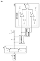
- FIG. It is a figure which shows the drive control circuit of the power semiconductor element of Embodiment 1.
- FIG. It is a figure for demonstrating the detection principle of an arm short circuit based on the relationship between the gate current Ig and the gate charge amount Qg.
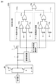
- FIG. 1 is a diagram showing a drive control circuit for a power semiconductor element according to the first embodiment.
- the power semiconductor element 1 is one of a Si-IGBT, an RC (Reverse Conducting) -IGBT, a SiC- MOSFET, a GaN transistor, and a Ga2O3 transistor. In the following description, a MOSFET will be described as an example of the power semiconductor element 1.
- the power semiconductor element 1 has a control electrode, a positive electrode, and a negative electrode.
- the drive control circuit of this power semiconductor element includes a commander 2, a driver 80, a resistor 7, a current sensor 8 functioning as a gate current detector, a gate charge amount calculator 9, and a short-circuit detector 300. To prepare for.
- the command device 2 outputs a command to turn on or a command to turn off the power semiconductor element 1 to the drive device 80.
- the command to turn on is a high level signal.
- the command to turn off is a low level signal.
- the power semiconductor element 1 transitions between a conduction (on) state and a cutoff (off) state based on a signal from the commander 2.
- the resistance 7 is arranged between the drive 80 and the power semiconductor element 1.
- the drive 80 includes a transistor 5 and a transistor 6.
- the transistor 5 Upon receiving the turn-on command, the transistor 5 is in a conductive state and the transistor 6 is in a non-conducting state.
- the positive gate voltage source 3 is connected to the control electrode of the power semiconductor element 1 via the resistor 7, so that the power semiconductor element 1 is in a conductive state.
- the transistor 5 When the command to turn off is received, the transistor 5 is in the non-conducting state and the transistor 6 is in the conducting state. As a result, the reference potential 4 is connected to the control electrode of the power semiconductor element 1 via the resistor 7, so that the power semiconductor element 1 is in a non-conducting state.
- the current sensor 8 is placed between the drive 80 and the control electrode of the power semiconductor element 1 when the power semiconductor element 1 is in a conductive state (during turn-on operation) and when it is in a non-conducting state (during turn-off operation). Detects the gate current Ig flowing through. Specifically, the current sensor 8 detects the magnitude of the current flowing in the wiring between the drive 80 and the control electrode of the power semiconductor element 1. The current sensor 8 outputs a voltage signal indicating the magnitude of the gate current Ig to the gate charge amount calculator 9 and the gate current determination device 101.
- the gate charge amount calculator 9 receives a voltage signal indicating the magnitude of the gate current Ig from the current sensor 8. The gate charge amount calculator 9 calculates the gate charge amount Qg by integrating the gate current.
- the short circuit detector 300 detects an arm short circuit or a load short circuit based on the magnitude of the gate current Ig and the magnitude of the gate charge amount Qg. In this embodiment, an arm short circuit is detected.
- the short-circuit detector 300 includes a gate current determination device 101, a gate charge amount determination device 11, and an arm short-circuit detection logic operation device 18.
- the gate current determination device 101 determines whether or not the gate current Ig is the gate current lower limit reference value 104 or more and the gate current upper limit reference value 14 or less.
- the gate current determination device 101 outputs a high-level signal when the gate current Ig is the gate current lower limit reference value 104 or more and the gate current upper limit reference value 14 or less.
- the gate current determining device 101 includes a first comparator 102 for gate current, a second comparator 10 for gate current, and a logic operation unit 107 for gate current.
- the first comparator 102 for gate current compares the output signal of the current sensor 8 with the gate current lower limit reference value 104.
- the first comparator 102 for gate current outputs a high-level signal when the output signal of the current sensor 8 is equal to or higher than the gate current lower limit reference value 104.
- the second comparator 10 for gate current compares the output signal of the current sensor 8 with the gate current upper limit reference value 14.
- the second comparator 10 for gate current outputs a high-level signal when the output signal of the current sensor 8 is equal to or less than the gate current upper limit reference value 14.
- the gate current logical operation unit 107 outputs the logical product of the output signal of the second comparator 10 for gate current and the output signal of the first comparator 102 for gate current.
- the gate charge amount determining device 11 determines whether or not the gate charge amount Qg is equal to or more than the gate charge amount lower limit reference value 15 and the gate charge amount upper limit reference value 16 or less.
- the gate charge amount determining device 11 outputs a high-level signal when the gate charge amount Qg is the gate charge amount lower limit reference value 15 or more and the gate charge amount upper limit reference value 16 or less.
- the gate charge amount determining device 11 includes a first comparator 12 for the gate charge amount, a second comparator 13 for the gate charge amount, and a logical operation unit 17 for the gate charge amount.
- the first comparator 12 for the gate charge amount compares the output signal (gate charge amount Qg) of the gate charge amount calculator 9 with the gate charge amount lower limit reference value 15.
- the first comparator 12 for the gate charge amount outputs a high-level signal when the output signal (gate charge amount Qg) of the gate charge amount calculator 9 is equal to or more than the gate charge amount lower limit reference value 15.
- the second comparator 13 for the gate charge amount compares the output signal (gate charge amount Qg) of the gate charge amount calculator 9 with the gate charge amount upper limit reference value 16.
- the second comparator 13 for the gate charge amount outputs a high-level signal when the output signal (gate charge amount Qg) of the gate charge amount calculator 9 is equal to or less than the gate charge amount upper limit reference value 16.
- the gate charge amount logical operation unit 17 outputs the logical product of the output signal of the first comparator 12 for the gate charge amount and the output signal of the second comparator 13 for the gate charge amount.
- the arm short circuit detection logical operation unit 18 calculates the logical product of the output signal of the gate current logical operation unit 107 of the gate current determination unit 101 and the output signal of the gate charge amount logical operation unit 17 of the gate charge amount determination unit 11. By asking, an arm short circuit is detected.
- the arm short-circuit detection logical operation unit 18 is in an arm short-circuit state only when the output signal of the gate current logical operation unit 107 is at a high level and the output signal of the gate charge amount logical operation unit 17 is at a high level. Detects and outputs a high level signal indicating that the arm is short-circuited.
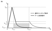
- FIG. 2 is a diagram for explaining the principle of detecting an arm short circuit based on the relationship between the gate current Ig and the gate charge amount Qg.
- the power semiconductor element 1 and the power semiconductor element of the reverse arm that operates complementarily to the power semiconductor element 1 are turned on at the same time.
- the waveform shown by the broken line shows the relationship between the gate current Ig and the gate charge amount Qg during normal switching operation.
- the waveform shown by the solid line shows the relationship between the gate current Ig and the gate charge amount Qg during the arm short-circuit operation.
- the gate current Ig increases with time and decreases after a peak value (Igmax). After that, the gate current Ig decreases again after a period (mirror period) at which the constant current value (Im) is reached. On the other hand, in the arm short-circuit operation, the gate current Ig reaches a peak value (Igmax) and then decreases monotonically without a period of a constant value (mirror period).
- the drive control circuit of the power semiconductor element of the present embodiment detects an arm short-circuit state by utilizing such a difference.
- the gate current upper limit reference value 14 is set to a value (Vref_ig2) smaller than the gate current value (Im) during the mirror period during normal switching operation.
- the gate current lower limit reference value 104 is set to a value higher than zero (Vref_ig1).
- the gate charge amount lower limit reference value 15 is set to a value (Vref_q1) in which the gate current is larger than the gate charge amount at the peak value (Igmax) during normal switching operation.
- the gate charge amount upper limit reference value 16 is set to a value (Vref_q2) smaller than the gate charge amount at the end of the mirror period during normal switching operation.
- the gate current determination device 101 operates as follows.
- the gate charge amount determining device 11 operates as follows.
- the drive control circuit for the power semiconductor element of the present embodiment outputs a high-level signal when the power semiconductor element 1 is in the arm short-circuited state.
- the drive control circuit of the power semiconductor element of the present embodiment can quickly detect and protect an arm short circuit without setting a detection period for determining a short circuit state. Further, the drive control circuit for the power semiconductor element of the present embodiment is highly reliable, inexpensive, and can reduce the circuit scale.
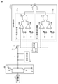
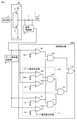
- FIG. 3 is a diagram showing a drive control circuit of the power semiconductor element according to the second embodiment.
- the difference between the drive control circuit of the power semiconductor element of the second embodiment of FIG. 3 and the power semiconductor element 1 of the first embodiment of FIG. 1 is that the drive control circuit of the power semiconductor element of the second embodiment is The point is that the drive device 80a is provided in place of the drive device 80, and the short circuit detector 300a is provided in place of the short circuit detector 300.
- the short-circuit detector 300a includes the gate charge amount determination device 11 similar to that of the first embodiment, and includes a gate current determination device 101a instead of the gate current determination device 101.
- the drive 80a includes an on-switch circuit 19 and an off-switch circuit 20.
- the on-switch circuit 19 includes a positive gate voltage source 3, a transistor 5, and an on-gate resistor 7a.
- the off-switch circuit 20 includes a reference potential 4, a transistor 6, and an off-gate resistance 7b.
- the positive gate voltage source 3, the transistor 5, the on-gate resistance 7a, the off-gate resistance 7b, the transistor 6, and the reference potential 4 are connected in series.
- the control electrode of the power semiconductor element 1 is connected to the node ND1 to which the on-gate resistance 7a and the off-gate resistance 7b are connected.
- the current sensor 8 detects the current flowing from the transistor 5 to the on-gate resistance 7a.
- the current sensor 8 detects the gate current flowing into the control electrode of the power semiconductor element 1 when the power semiconductor element 1 is brought into a conductive state (during turn-on operation).
- the current sensor 8 sends a voltage signal representing the detection result to the gate charge amount calculator 9 and the gate current determination device 101a.
- the current sensor 8 detects the current between the node ND1 and the power semiconductor element 1, so that the current sensor 8 detects the gate current in both the turn-on operation and the turn-off operation. ..
- the current sensor 8 detects the current flowing through the on-switch circuit 19, so that the current sensor 8 detects the gate current flowing into the control electrode of the power semiconductor element 1 only during the turn-on operation.
- the arm short-circuit detection logical operation unit 18 may detect the arm short-circuit even during the turn-off operation.
- the current sensor 8 detects the gate current only during the turn-on operation, so that the possibility of erroneous detection can be eliminated.
- the gate current determination device 101a determines whether or not the gate current Ig is equal to or less than the gate current upper limit reference value 14.
- the gate current determination device 101a outputs a high-level signal when the gate current Ig is equal to or less than the gate current upper limit reference value 14.
- the gate current determination device 101a includes a second comparator 10 for gate current.
- the second comparator 10 for gate current compares the output signal of the current sensor 8 with the gate current upper limit reference value 14.
- the second comparator 10 for gate current outputs a high-level signal when the output signal of the current sensor 8 is equal to or less than the gate current upper limit reference value 14.
- the gate current Ig detected by the current sensor 8 is only a positive value. Since it is not necessary to detect whether or not the gate current Ig is higher than 0, the gate current determination device 101a includes only the second comparator 10 for the gate current.
- the logical operation unit 18 for detecting an arm short circuit is a logic between the output signal of the second comparator 10 for the gate current of the gate current determination unit 101a and the output signal of the logical operation unit 17 for the gate charge amount of the gate charge amount determination unit 11.
- An arm short circuit is detected by determining the product.
- the arm short-circuit detection logical operation unit 18 is in the arm short-circuit state only when the output signal of the second comparator 10 for gate current is high level and the output signal of the logical operation unit 17 for gate charge amount is high level. Detects the presence and outputs a high-level signal indicating that the arm is short-circuited.
- FIG. 3 shows a configuration in which a resistance is not connected between the node ND1 to which the on-gate resistance 7a and the off-gate resistance 7b are connected and the control electrode of the power semiconductor element 1, but the node ND1 and the power semiconductor element 1 are shown.
- a resistor may be connected between the control electrodes.
- FIG. 4 is a diagram showing a drive control circuit of the power semiconductor element according to the third embodiment.
- the difference between the drive control circuit of the power semiconductor element of the third embodiment of FIG. 4 and the power semiconductor element 1 of the first embodiment of FIG. 1 is that the drive control circuit of the power semiconductor element of the third embodiment is ,
- a differential amplifier 21 is provided instead of the current sensor 8.
- the differential amplifier 21 detects the gate current Ig flowing between the drive 80 and the control electrode of the power semiconductor element 1 by detecting the voltage across the resistor 7.
- the output signal of the differential amplifier 21 is sent to the gate charge amount calculator 9 and the gate current determination device 101.
- the gate charge amount calculator 9 receives a voltage signal indicating the magnitude of the gate current Ig from the differential amplifier 21.
- the gate charge amount calculator 9 calculates the gate charge amount Qg by integrating the gate current Ig.
- the first comparator 102 for gate current compares the output signal of the differential amplifier 21 with the gate current lower limit reference value 104.
- the first comparator 102 for gate current outputs a high-level signal when the output signal of the differential amplifier 21 is equal to or higher than the gate current lower limit reference value 104.
- the second comparator 10 for gate current compares the output signal of the differential amplifier 21 with the gate current upper limit reference value 14.
- the second comparator 10 for gate current outputs a high-level signal when the output signal of the differential amplifier 21 is equal to or less than the gate current upper limit reference value 14.
- FIG. 5 is a diagram showing a drive control circuit of the power semiconductor element of the fourth embodiment.
- the difference between the drive control circuit of the power semiconductor element of the fourth embodiment of FIG. 5 and the power semiconductor element 1 of the second embodiment of FIG. 3 is that the drive control circuit of the power semiconductor element of the fourth embodiment is ,
- a differential amplifier 21 is provided instead of the current sensor 8.
- the differential amplifier 21 detects the gate current Ig flowing into the control electrode of the power semiconductor element 1 by detecting the voltage across the on-gate resistor 7a.
- the output signal of the differential amplifier 21 is sent to the gate charge amount calculator 9 and the gate current determination device 101. Subsequent operations are the same as in the first embodiment.
- FIG. 6 is a diagram showing a drive control circuit of the power semiconductor element according to the fifth embodiment.
- the difference between the drive control circuit of the power semiconductor element of the fifth embodiment of FIG. 6 and the power semiconductor element 1 of the third embodiment of FIG. 4 is that the drive control circuit of the power semiconductor element of the fifth embodiment is The point is that the protection circuit 400 is provided.
- the protection circuit 400 When the short circuit detector 300 detects an arm short circuit or a load short circuit, the protection circuit 400 outputs a command to turn off the power semiconductor element 1 to the drive device 80 regardless of the command of the command device 2.
- the protection circuit 400 includes a latch circuit 22, an inverting circuit 23, and a logical operation unit 24.
- the latch circuit 22 holds a high-level signal when the output signal of the arm short-circuit detection logical operation unit 18 changes from a low-level signal to a high-level signal.
- the held output signal is sent to the inverting circuit 23.
- the inverting circuit 23 inverts the level of the output signal of the latch circuit 22.
- the logical operation unit 24 outputs the logical product of the output signal of the command unit 2 and the output signal of the inverting circuit 23 to the drive unit 80.
- the transistor 5 and the transistor 6 control the power semiconductor element 1 so as to be in a conductive state or a cutoff state.
- the arm short-circuit detection logical operation unit 18 outputs a low-level signal.
- the latch circuit 22 outputs a low-level signal to the inverting circuit 23.
- the inverting circuit 23 outputs a high level signal. Since the output signal of the inverting circuit 23 is high level, the logical operation unit 24 outputs the high level signal to the drive unit 80 when the signal from the commander 2 is high level. As a result, in the driver 80, the transistor 5 is turned on and the transistor 6 is turned off, so that the power semiconductor element 1 is in a conductive state.
- the arm short circuit detection logical operation unit 18 When an arm short circuit is detected by the arm short circuit detection logical operation unit 18, the arm short circuit detection logical operation unit 18 outputs a high-level signal.
- the latch circuit 22 holds a high-level output signal output from the arm short-circuit detection logical operation unit 18 and outputs the high-level output signal to the inverting circuit 23.
- the inverting circuit 23 outputs a low level signal. Since the output signal of the inverting circuit 23 is low level, the logical operation unit 24 outputs the low level signal to the drive unit 80 regardless of the level of the signal from the commander 2.
- the driver 80 the transistor 5 is turned off and the transistor 6 is turned on, so that the power semiconductor element 1 is cut off. As a result, the power semiconductor element 1 is protected.
- the differential amplifier 21 detects the voltage across the resistor 7 connected to the control electrode of the power semiconductor element 1 to detect the voltage across the power semiconductor element 1.
- the amount of electricity corresponding to the gate current is detected, but the present invention is not limited to this.
- the current sensor 8 may detect the amount of electricity corresponding to the gate current.
- the amount of electricity corresponding to the gate current of the power semiconductor element 1 may be detected by detecting the voltage across the on-gate resistance 7a.
- FIG. 7 is a diagram showing a drive control circuit of the power semiconductor element according to the sixth embodiment.
- the difference between the drive control circuit of the power semiconductor element of the sixth embodiment of FIG. 7 and the power semiconductor element 1 of the third embodiment of FIG. 4 is that the drive control circuit of the power semiconductor element of the sixth embodiment is ,
- the filter 25 is provided.
- the filter 25 receives the output signal of the differential amplifier 21.
- the filter 25 shapes the waveform of the output signal of the differential amplifier 21 with a predetermined time constant. Since the filter 25 slows down the time change of the output signal of the differential amplifier 21, it is possible to prevent erroneous detection of an arm short circuit.
- the output of the filter 25 is sent to the gate charge amount calculator 9, the first comparator 102 for the gate current of the short circuit detector 300, and the second comparator 10 for the gate current.
- the differential amplifier 21 detects the voltage across the resistor 7 connected to the control electrode of the power semiconductor element 1 to detect the voltage across the power semiconductor element 1.
- the amount of electricity corresponding to the gate current is detected, but the present invention is not limited to this.
- the current sensor 8 may detect the amount of electricity corresponding to the gate current.
- the amount of electricity corresponding to the gate current of the power semiconductor element 1 may be detected by detecting the voltage across the on-gate resistance 7a.
- the power semiconductor element 1 may be transitioned to the cutoff state by the protection circuit 400.
- FIG. 8 is a diagram showing a drive control circuit of the power semiconductor element according to the seventh embodiment.
- the difference between the drive control circuit of the power semiconductor element of the seventh embodiment of FIG. 8 and the power semiconductor element 1 of the third embodiment of FIG. 4 is that the drive control circuit of the power semiconductor element of the seventh embodiment is ,
- a short-circuit detector 300b is provided instead of the short-circuit detector 300.
- the short-circuit detector 300b includes a gate current determination device 101b instead of the gate current determination device 101, a gate charge amount determination device 11a instead of the gate charge amount determination device 11, and an arm short-circuit detection logic operation unit 18. Instead, a logical operation unit 18a for detecting an arm short circuit is provided.
- the gate current determination device 101b determines whether or not the gate current Ig is the gate current lower limit reference value 104 or more and the gate current upper limit reference value 14 or less.
- the gate current determination device 101b outputs a low-level signal when the gate current Ig is the gate current lower limit reference value 104 or more and the gate current upper limit reference value 14 or less.
- the gate current determination device 101b includes a first comparator 102a for gate current, a second comparator 10a for gate current, and a logic operation unit 107a for gate current.
- the first comparator 102a for gate current compares the output signal of the differential amplifier 21 with the gate current lower limit reference value 104.
- the first comparator 102a for gate current outputs a low-level signal when the output signal of the differential amplifier 21 is equal to or higher than the gate current lower limit reference value 104.
- the second comparator 10a for gate current compares the output signal of the differential amplifier 21 with the gate current upper limit reference value 14.
- the second comparator 10a for gate current outputs a low level signal when the output signal of the differential amplifier 21 is equal to or less than the gate current upper limit reference value 14.
- the gate current logical operation unit 107a performs an exclusive OR operation between the output signal of the first comparator 102a for gate current and the output signal of the second comparator 10a for gate current.
- the gate current logical operation unit 107a outputs a low level signal when the output signal of the first comparator 102a for gate current is low level and the output signal of the second comparator 10a for gate current is low level. do.
- Logical operation for gate current considering that the output signal of the first comparator 102a for gate current is high level and the output signal of the second comparator 10a for gate current cannot be high level.
- the unit 107a is an exclusive OR operation unit, it may be an OR operation unit.
- the gate charge amount determining device 11a determines whether or not the gate charge amount Qg is equal to or more than the gate charge amount lower limit reference value 15 and the gate charge amount upper limit reference value 16 or less.
- the gate charge amount determining device 11a outputs a low-level signal when the gate charge amount Qg is equal to or more than the gate charge amount lower limit reference value 15 and the gate charge amount upper limit reference value 16 or less.
- the gate charge amount determining device 11a includes a first comparator 12a for the gate charge amount, a second comparator 13a for the gate charge amount, and a logical operation unit 17a for the gate charge amount.
- the first comparator 12a for the gate charge amount compares the output signal of the gate charge amount calculator 9 with the gate charge amount lower limit reference value 15.
- the first comparator 12a for the gate charge amount outputs a low-level signal when the output signal of the gate charge amount calculator 9 is the gate charge amount lower limit reference value 15 or more.
- the second comparator 13a for the gate charge amount compares the output signal of the gate charge amount calculator 9 with the gate charge amount upper limit reference value 16.
- the second comparator 13a for the gate charge amount outputs a low-level signal when the output signal of the gate charge amount calculator 9 is equal to or less than the gate charge amount upper limit reference value 16.
- the gate charge amount logical operation unit 17a performs an exclusive OR operation between the output signal of the first comparator 12 for the gate charge amount and the output signal of the second comparator 13 for the gate charge amount.
- the logic operation unit 17a outputs a low level signal when the output signal of the first comparator 12a for the gate charge amount is low level and the output signal of the second comparator 13a for the gate charge amount is low level. .. Considering that the output signal of the first comparator 12 for the gate charge amount is high level and the output signal of the second comparator 13 for the gate charge amount cannot be high level, the gate charge amount
- the logical operation unit 17a is an exclusive OR operation unit, it may be an OR operation unit.
- the logical operation unit 18a for detecting an arm short circuit detects an arm short circuit based on a logical sum calculation of the output signal of the gate current determination device 101 and the output signal of the gate charge amount determination device 11.
- the output signal of the gate current determination device 101b is low level (the gate current Ig is the gate current upper limit reference value 14 or less and the gate current lower limit reference value 104 or more), and the gate charge amount determination device 11a. Only when the output signal of is low level (gate charge amount Qg is gate charge amount lower limit reference value 15 or more and gate charge amount upper limit reference value 16 or less), arm short circuit is detected to indicate that arm short circuit has occurred. Outputs a low level signal.
- the differential amplifier 21 detects the voltage across the resistor 7 connected to the control electrode of the power semiconductor element 1 to detect the voltage across the power semiconductor element 1.
- the amount of electricity corresponding to the gate current is detected, but the present invention is not limited to this.
- the current sensor 8 may detect the amount of electricity corresponding to the gate current.
- the amount of electricity corresponding to the gate current of the power semiconductor element 1 may be detected by detecting the voltage across the on-gate resistance 7a.
- the power semiconductor element 1 may be transitioned to the cutoff state by the protection circuit 400.
- FIG. 9 is a diagram showing a drive control circuit of the power semiconductor element according to the eighth embodiment.
- the difference between the drive control circuit of the power semiconductor element of the eighth embodiment of FIG. 9 and the power semiconductor element 1 of the third embodiment of FIG. 4 is that the drive control circuit of the power semiconductor element of the eighth embodiment is ,
- a short circuit detector 300c is provided instead of the short circuit detector 300.
- the short-circuit detector 300c includes a gate current determination device 101c instead of the gate current determination device 101, and a gate charge amount determination device 11b instead of the gate charge amount determination device 11.
- the difference between the gate current determination device 101c and the gate current determination device 101 is that the gate current determination device 101c includes a second comparator 10b for gate current instead of the second comparator 10 for gate current.
- the second comparator 10b for gate current compares the output signal of the differential amplifier 21 with the variable gate current upper limit reference value 14b.
- the second comparator 10b for gate current outputs a high-level signal when the output signal of the differential amplifier 21 is equal to or less than the variable gate current upper limit reference value 14b.
- the gate current upper limit reference value 14 is set to a value (Vref_ig2) smaller than the gate current value (Im) during the mirror period.
- the gate current value Im during the mirror period is determined by the output characteristics of the power semiconductor element 1 and the resistance value between the positive gate voltage source 3 and the control electrode of the power semiconductor element 1. Since the output characteristics of the power semiconductor device 1 are temperature-dependent, the gate current value Im during the mirror period is temperature-dependent.
- the gate current upper limit reference value 14b is set to change according to the temperature. As a result, an appropriate value can be set to the gate current upper limit reference value 14b according to the operating environment of the power semiconductor element 1, so that the arm short-circuit state can be reliably detected.
- the difference between the gate charge amount determination device 11b and the gate charge amount determination device 11 is that the gate charge amount determination device 11b is a first comparison device 12b for the gate charge amount instead of the first comparison device 12 for the gate charge amount. , And instead of the second comparator 13 for the gate charge amount, the second comparator 13b for the gate charge amount is provided.
- the first comparator 12b for the gate charge amount compares the output signal (gate charge amount Qg) of the gate charge amount calculator 9 with the variable gate charge amount lower limit reference value 15b.
- the first comparator 12b for the gate charge amount outputs a high-level signal when the output signal (gate charge amount Qg) of the gate charge amount calculator 9 is equal to or higher than the variable gate charge amount lower limit reference value 15b.
- the second comparator 13b for the gate charge amount compares the output signal (gate charge amount Qg) of the gate charge amount calculator 9 with the variable gate charge amount upper limit reference value 16b.
- the second comparator 13 for the gate charge amount outputs a high-level signal when the output signal (gate charge amount Qg) of the gate charge amount calculator 9 is equal to or less than the variable gate charge amount upper limit reference value 16b.
- the gate charge amount lower limit reference value 15 is set to a value (Vref_q1) in which the gate current is larger than the charge amount at the peak value (Igmax).
- the gate charge amount upper limit reference value 16 is set to a value (Vref_q2) smaller than the gate charge amount at the end of the mirror period.
- the gate current Ig that flows during the mirror period flows through the feedback capacitance of the power semiconductor element 1.
- the feedback capacitance is a parasitic capacitance between the positive electrode side electrode and the control electrode of the power semiconductor element 1.
- the amount of electric charge supplied during the mirror period has a dependency on the voltage applied between the positive electrode side electrode and the negative electrode side electrode of the power semiconductor element 1.
- the gate charge amount lower limit reference value 15b and the gate charge amount upper limit reference value 16b are set so as to change according to the voltage applied to the positive electrode side electrode and the negative electrode side electrode of the power semiconductor element 1.
- the gate charge amount lower limit reference value 15b and the gate charge amount upper limit reference value 16b can be appropriately set according to the operating environment of the power semiconductor element 1, so that the arm short-circuit state can be reliably detected. ..
- the differential amplifier 21 detects the voltage across the resistor 7 connected to the control electrode of the power semiconductor element 1 to detect the voltage across the power semiconductor element 1.
- the amount of electricity corresponding to the gate current is detected, but the present invention is not limited to this.
- the current sensor 8 may detect the amount of electricity corresponding to the gate current.
- the amount of electricity corresponding to the gate current of the power semiconductor element 1 may be detected by detecting the voltage across the on-gate resistance 7a.
- the power semiconductor element 1 may be transitioned to the cutoff state by the protection circuit 400 when the arm is short-circuited.
- FIG. 10 is a diagram showing a drive control circuit of the power semiconductor element according to the ninth embodiment.
- the difference between the drive control circuit of the power semiconductor element of the ninth embodiment of FIG. 10 and the power semiconductor element 1 of the third embodiment of FIG. 4 is that the drive control circuit of the power semiconductor element of the ninth embodiment is The point is that the initialization calculator 26 is provided.
- the initialization calculator 26 initializes the output signal of the gate charge amount calculator 9 to zero in response to the timing at which the gate current Ig starts to flow during the turn-on operation of the power semiconductor element 1.
- the gate charge amount calculator 9 can accurately calculate the gate charge amount Qg, so that it is possible to prevent the arm short-circuit detection logic calculator 18 from erroneously detecting the arm short-circuit.
- the differential amplifier 21 detects the voltage across the resistor 7 connected to the control electrode of the power semiconductor element 1 to detect the voltage across the power semiconductor element 1.
- the amount of electricity corresponding to the gate current is detected, but the present invention is not limited to this.
- the current sensor 8 may detect the amount of electricity corresponding to the gate current.
- the amount of electricity corresponding to the gate current of the power semiconductor element 1 may be detected by detecting the voltage across the on-gate resistance 7a.
- the power semiconductor element 1 may be transitioned to the cutoff state by the protection circuit 400 when the arm is short-circuited.
- the arm short circuit has been described as a short circuit state, but in the short circuit state, in addition to the arm short circuit, there is a load short circuit in which the load of the motor or the like connected to the power semiconductor element 1 is in the short circuit state.
- the load is short-circuited, the voltage between the positive electrode and the negative electrode of the power semiconductor element 1 (drain-source voltage) drops to the on-voltage, and then the drain current sharply increases, as in the normal turn-on operation. At the same time, the voltage between the drain and the source rises.
- the capacitance between the drain and the gate becomes smaller, and a current flows from the drain terminal of the power semiconductor element 1 to the drive 80 via the gate terminal. Turns negative and the gate charge amount Qg decreases.
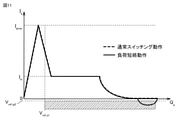
- FIG. 11 is a diagram for explaining the principle of detecting a load short circuit based on the relationship between the gate current Ig and the gate charge amount Qg.
- the waveform shown by the broken line shows the relationship between the gate current Ig and the gate charge amount Qg during normal switching operation.
- the waveform shown by the solid line shows the relationship between the gate current Ig and the gate charge amount Qg during the load short-circuit operation.
- the relationship between the gate current Ig and the gate charge amount Qg is the same as during normal switching operation up to the middle even in the load short-circuit state. That is, the gate current Ig increases with time and decreases after a peak value (Igmax). After that, the current decreases again after a period (mirror period) at which the current value becomes constant (Im).
- the gate current Ig turns negative as described above. That is, the gate current Ig flows from the power semiconductor element 1 to the drive 80. Since the gate current Ig becomes negative, the gate charge amount Qg expressed as the time integral of the gate current Ig decreases.
- the drive control circuit of the power semiconductor element of the present embodiment determines the load short-circuit state by utilizing such a difference.
- the gate current upper limit reference value 14c is set to a value smaller than zero (Vref_ig2).
- the gate charge amount lower limit reference value 15 is set to a value (Vref_q1) in which the gate current is larger than the charge amount at the peak value (Igmax).
- FIG. 12 is a diagram showing a drive control circuit of the power semiconductor element according to the tenth embodiment.
- the difference between the drive control circuit of the power semiconductor element of the tenth embodiment of FIG. 12 and the power semiconductor element 1 of the third embodiment of FIG. 4 is that the drive control circuit of the power semiconductor element of the tenth embodiment is ,
- a short-circuit detector 300d is provided in place of the short-circuit detector 300.
- the short-circuit detector 300d replaces the gate current determination device 101, the gate charge amount determination device 11, and the arm short-circuit detection logic operation unit 18, with the gate current determination device 101d, the gate charge amount determination device 11c, and the load short-circuit detection device.
- a logical operation unit 56 is provided.
- the gate current determination device 101d determines whether or not the gate current Ig is equal to or less than the gate current upper limit reference value 14c.
- the gate current determination device 101d outputs a high-level signal when the gate current Ig is equal to or less than the gate current upper limit reference value 14c.
- the gate current determination device 101d includes a third comparator 50 for gate current.
- the third comparator 50 for gate current compares the output signal of the differential amplifier 21 with the gate current upper limit reference value 14c.
- the third comparator 50 for gate current outputs a high-level signal when the output signal of the differential amplifier 21 is equal to or less than the gate current upper limit reference value 14c.
- the gate charge amount determining device 11c determines whether or not the gate charge amount Qg is equal to or more than the gate charge amount lower limit reference value 15.
- the gate charge amount determining device 11c outputs a high-level signal when the gate charge amount Qg is equal to or higher than the gate charge amount lower limit reference value 15.
- the gate charge amount determining device 11c includes a first comparator 12 for the gate charge amount.
- the first comparator 12 for the gate charge amount compares the output signal (gate charge amount Qg) of the gate charge amount calculator 9 with the gate charge amount lower limit reference value 15.
- the first comparator 12 for the gate charge amount outputs a high-level signal when the output signal (gate charge amount Qg) of the gate charge amount calculator 9 is equal to or more than the gate charge amount lower limit reference value 15.
- the load short circuit detection logical operation unit 56 includes an output signal of the third comparator 50 for the gate current of the gate current determination device 101d and an output signal of the first comparator 12 for the gate charge amount of the gate charge amount determination device 11c. Outputs the logical product of and.
- the load short-circuit detection logical operation unit 56 determines that the load is in a short-circuited state when the gate current Ig is the gate current upper limit reference value 14c or less and the gate charge amount Qg is the gate charge amount lower limit reference value 15 or more. , Outputs a high level signal indicating that the load is short-circuited.
- the differential amplifier 21 detects the voltage across the resistor 7 connected to the control electrode of the power semiconductor element 1 to detect the voltage across the power semiconductor element 1.
- the amount of electricity corresponding to the gate current is detected, but the present invention is not limited to this.
- the current sensor 8 may detect the amount of electricity corresponding to the gate current.
- the amount of electricity corresponding to the gate current of the power semiconductor element 1 may be detected by detecting the voltage across the on-gate resistance 7a.
- the power semiconductor element 1 may be transitioned to the cutoff state by the protection circuit 400.
- FIG. 13 is a diagram showing a drive control circuit of the power semiconductor element according to the eleventh embodiment.
- the difference between the drive control circuit of the power semiconductor element of the eleventh embodiment of FIG. 13 and the power semiconductor element 1 of the first embodiment of FIG. 1 is that the drive control circuit of the power semiconductor element of the eleventh embodiment is Further, a third comparator 50 for gate current and a logic calculator 56 for detecting a load short circuit, which are the same as those in the tenth embodiment, are provided. Further, the drive control circuit for the power semiconductor element according to the eleventh embodiment includes a short circuit determination device 118.
- the first comparator 12 for the gate charge amount included in the gate charge amount determination device 11 is used for both the detection of the arm short circuit and the detection of the load short circuit.
- the third comparator 50 for gate current compares the output signal of the differential amplifier 21 with the gate current upper limit reference value 14c.
- the third comparator 50 for gate current outputs a high-level signal when the output signal of the differential amplifier 21 is equal to or less than the gate current upper limit reference value 14c.
- the first comparator 12 for the gate charge amount compares the output signal (gate charge amount Qg) of the gate charge amount calculator 9 with the gate charge amount lower limit reference value 15.
- the first comparator 12 for the gate charge amount outputs a high-level signal when the output signal (gate charge amount Qg) of the gate charge amount calculator 9 is equal to or more than the gate charge amount lower limit reference value 15.
- the load short circuit detection logical operation unit 56 outputs the logical product of the output signal of the third comparator 50 for the gate current and the output signal of the first comparator 12 for the gate charge amount.
- the load short-circuit detection logic operation unit 56 determines that the load is short-circuited when the gate current Ig is the gate current upper limit reference value 14c or less and the gate charge amount Qg is the gate charge amount lower limit reference value 15 or more. Outputs a high-level signal indicating that the load is short-circuited.
- the short circuit determination device 118 outputs the logical sum of the output signal of the logical operation unit 18 for arm short circuit detection and the output signal of the logical operation unit 56 for load short circuit detection.
- the short circuit determination unit 118 outputs a high level signal indicating a short circuit when at least one of the output signal of the arm short circuit detection logical operation unit 18 and the output signal of the load short circuit detection logical operation unit 56 is high level. do.
- both the arm short circuit and the load short circuit can be detected, so that the power semiconductor element can be protected more reliably.
- the short circuit determination device 118 when at least one of the load short circuit and the arm short circuit is detected, the short circuit determination device 118 outputs a high level signal, but the present invention is not limited to this. As in the seventh embodiment, the short circuit determination device 118 may output a low level signal by reversing the logic.
- the differential amplifier 21 detects the voltage across the resistor 7 connected to the control electrode of the power semiconductor element 1 to detect the voltage across the power semiconductor element 1.
- the amount of electricity corresponding to the gate current is detected, but the present invention is not limited to this.
- the current sensor 8 may detect the amount of electricity corresponding to the gate current.
- the amount of electricity corresponding to the gate current of the power semiconductor element 1 may be detected by detecting the voltage across the on-gate resistance 7a.
- the power semiconductor element 1 may be transitioned to the cutoff state by the protection circuit 400.
- Embodiment 12 the power semiconductor element 1 and the drive control circuit of the above-described embodiment are applied to a power conversion device.
- the present disclosure is not limited to a specific power conversion device, the case where the present disclosure is applied to a three-phase inverter will be described below as an embodiment.
- FIG. 14 is a block diagram showing the configuration of the power conversion system according to the twelfth embodiment.
- the power conversion system includes a power supply 700, a power conversion device 800, and a load 900.
- the power supply 700 is a DC power supply that supplies DC power to the power conversion device 800.
- the power supply 700 can be configured with various things.
- the power supply 700 may be composed of a DC system, a solar cell, a storage battery, a rectifier circuit connected to an AC system, or an AC / DC converter.
- the power supply 700 may be configured by a DC / DC converter that converts the DC power output from the DC system into a predetermined power.
- the power converter 800 is a three-phase inverter connected between the power supply 700 and the load 900.
- the power conversion device 800 converts the DC power supplied from the power supply 700 into AC power, and supplies AC power to the load 900.
- the power conversion device 800 includes a main conversion circuit 801 that converts DC power into AC power and outputs it, and a control circuit 803 that outputs a control signal for controlling the main conversion circuit 801 to the main conversion circuit 801.
- the load 900 is a three-phase electric motor driven by AC power supplied from the power conversion device 800.
- the load 900 is not limited to a specific application, and may be an electric motor mounted on various electric devices.
- the load 900 is used as an electric motor for a hybrid vehicle, an electric vehicle, a railroad vehicle, an elevator, or an air conditioner.
- the main conversion circuit 801 includes a power semiconductor module 802.
- the power semiconductor module 802 includes a power semiconductor element 1 which is a switching element and a freewheeling diode (not shown). By switching the switching element, the DC power supplied from the power supply 700 is converted into AC power and supplied to the load 900.
- the power semiconductor module 802 according to the present embodiment is a two-level three-phase full bridge circuit, and has six switching elements and each. It is a two-level three-phase full bridge circuit composed of six freewheeling diodes antiparalleled to a switching element.
- each upper and lower arm constitutes each phase (U phase, V phase, W phase) of the full bridge circuit. Then, the output terminals of each upper and lower arm, that is, the three output terminals of the main conversion circuit 801 are connected to the load 900.
- the power semiconductor module 802 includes the drive control circuit described in the above embodiment.
- the drive control circuit drives each switching element.
- the drive control circuit is built in the power semiconductor module 802.
- the drive control circuit generates a drive signal for driving the switching element of the main conversion circuit 801 and supplies it to the control electrode of the switching element of the main conversion circuit 801. Specifically, the drive control circuit outputs a drive signal for turning on the switching element and a drive signal for turning off the switching element to the control electrode of each switching element according to the control signal from the control circuit 803.
- the drive signal is a voltage signal (on signal) equal to or higher than the threshold voltage of the switching element
- the drive signal is a voltage equal to or lower than the threshold voltage of the switching element. It becomes a signal (off signal).
- the control circuit 803 controls the switching element of the main conversion circuit 801 so that the desired power is supplied to the load 900. Specifically, the control circuit 803 calculates the time (on time) for each switching element of the main conversion circuit 801 to be in the on state based on the electric power to be supplied to the load 900. For example, the control circuit 803 can control the main conversion circuit 801 by PWM control that modulates the on-time of the switching element according to the voltage to be output. Then, the control circuit 803 is a drive control circuit provided in the main conversion circuit 801 so that an on signal is output to the switching element that should be turned on at each time point and an off signal is output to the switching element that should be turned off. Outputs a control command (control signal). The drive control circuit outputs an on signal or an off signal as a drive signal to the control electrode of each switching element according to this control signal.
- an example of applying the present disclosure to a two-level three-phase inverter has been described, but the present disclosure is not limited to this, and can be applied to various power conversion devices.
- an example of applying the present disclosure to a two-level power conversion device has been described, but it can be applied to a three-level or multi-level power conversion device.
- the present disclosure may be applied to a single-phase inverter when power is supplied to a single-phase load.
- the present disclosure can also be applied to a DC / DC converter or an AC / DC converter when power is supplied to a DC load or the like.
- the power conversion device to which the present disclosure is applied is not limited to the case where the above-mentioned load is an electric motor, for example, a discharge machine, a laser machine, an induction heating cooker, or a power supply device for a non-contact power supply system. It can also be used as a power conditioner for a photovoltaic power generation system or a power storage system.
Landscapes
- Power Conversion In General (AREA)
- Protection Of Static Devices (AREA)
- Electronic Switches (AREA)
Priority Applications (5)
| Application Number | Priority Date | Filing Date | Title |
|---|---|---|---|
| US18/014,174 US12149240B2 (en) | 2020-08-25 | 2020-08-25 | Drive control circuit for power semiconductor element, power semiconductor module, and power converter |
| CN202080104008.6A CN115997344A (zh) | 2020-08-25 | 2020-08-25 | 电力用半导体元件的驱动控制电路、电力用半导体模块以及电力变换装置 |
| PCT/JP2020/032033 WO2022044123A1 (ja) | 2020-08-25 | 2020-08-25 | 電力用半導体素子の駆動制御回路、電力用半導体モジュール、および電力変換装置 |
| JP2022544935A JP7471426B2 (ja) | 2020-08-25 | 2020-08-25 | 電力用半導体素子の駆動制御回路、電力用半導体モジュール、および電力変換装置 |
| DE112020007545.1T DE112020007545T5 (de) | 2020-08-25 | 2020-08-25 | Treiber-steuerungsschaltung für leistungshalbleiter-element, leistungshalbleiter-modul sowie stromrichter |
Applications Claiming Priority (1)
| Application Number | Priority Date | Filing Date | Title |
|---|---|---|---|
| PCT/JP2020/032033 WO2022044123A1 (ja) | 2020-08-25 | 2020-08-25 | 電力用半導体素子の駆動制御回路、電力用半導体モジュール、および電力変換装置 |
Publications (1)
| Publication Number | Publication Date |
|---|---|
| WO2022044123A1 true WO2022044123A1 (ja) | 2022-03-03 |
Family
ID=80354865
Family Applications (1)
| Application Number | Title | Priority Date | Filing Date |
|---|---|---|---|
| PCT/JP2020/032033 Ceased WO2022044123A1 (ja) | 2020-08-25 | 2020-08-25 | 電力用半導体素子の駆動制御回路、電力用半導体モジュール、および電力変換装置 |
Country Status (5)
| Country | Link |
|---|---|
| US (1) | US12149240B2 (https=) |
| JP (1) | JP7471426B2 (https=) |
| CN (1) | CN115997344A (https=) |
| DE (1) | DE112020007545T5 (https=) |
| WO (1) | WO2022044123A1 (https=) |
Cited By (1)
| Publication number | Priority date | Publication date | Assignee | Title |
|---|---|---|---|---|
| US20220190739A1 (en) * | 2020-12-14 | 2022-06-16 | Kabushiki Kaisha Toshiba | Power conversion apparatus |
Families Citing this family (3)
| Publication number | Priority date | Publication date | Assignee | Title |
|---|---|---|---|---|
| US20250096701A1 (en) * | 2023-09-14 | 2025-03-20 | GM Global Technology Operations LLC | Dynamic switching speed control to reduce loss, bearing current and electromagnetic interference |
| FR3161520A1 (fr) * | 2024-04-17 | 2025-10-24 | Stmicroelectronics International N.V. | Circuit de commande d’un transistor |
| CN119362360B (zh) * | 2024-12-25 | 2025-06-03 | 浙江创芯集成电路有限公司 | 检测电路及电压转换电路 |
Citations (5)
| Publication number | Priority date | Publication date | Assignee | Title |
|---|---|---|---|---|
| WO2007116900A1 (ja) * | 2006-04-06 | 2007-10-18 | Mitsubishi Electric Corporation | 半導体素子の駆動回路 |
| JP2009225506A (ja) * | 2008-03-13 | 2009-10-01 | Toshiba Corp | 電力変換器 |
| JP2015053749A (ja) * | 2013-09-05 | 2015-03-19 | 三菱電機株式会社 | 電力用半導体素子の駆動回路 |
| JP2019169825A (ja) * | 2018-03-23 | 2019-10-03 | 株式会社東芝 | 半導体装置及び電力変換装置 |
| WO2019207847A1 (ja) * | 2018-04-27 | 2019-10-31 | 三菱電機株式会社 | 電力用半導体素子の駆動装置 |
Family Cites Families (8)
| Publication number | Priority date | Publication date | Assignee | Title |
|---|---|---|---|---|
| DE10137875C1 (de) * | 2001-08-02 | 2003-04-30 | Dialog Semiconductor Gmbh | Lade/Entlade-Schutzschaltung |
| JP3883925B2 (ja) * | 2002-07-30 | 2007-02-21 | 三菱電機株式会社 | 電力用半導体素子の駆動回路 |
| KR101639488B1 (ko) * | 2014-12-10 | 2016-07-13 | 현대모비스 주식회사 | 암 쇼트 방지를 위한 게이트 구동 회로 및 방법 |
| EP3076009A3 (en) * | 2015-03-09 | 2017-01-04 | Fuji Electric Co., Ltd. | Semiconductor device |
| KR20170098062A (ko) * | 2016-02-19 | 2017-08-29 | 엘에스산전 주식회사 | 역병렬 사이리스터의 고장 검출기 |
| JP2017212870A (ja) * | 2016-05-20 | 2017-11-30 | 株式会社デンソー | スイッチング素子の駆動制御装置 |
| JP6610468B2 (ja) * | 2016-08-26 | 2019-11-27 | 株式会社デンソー | 半導体装置 |
| CN111244883B (zh) * | 2020-02-20 | 2021-09-21 | 南京航空航天大学 | 综合对比栅极电荷和电压的SiC MOSFET短路保护电路及保护方法 |
-
2020
- 2020-08-25 DE DE112020007545.1T patent/DE112020007545T5/de not_active Withdrawn
- 2020-08-25 US US18/014,174 patent/US12149240B2/en active Active
- 2020-08-25 JP JP2022544935A patent/JP7471426B2/ja active Active
- 2020-08-25 WO PCT/JP2020/032033 patent/WO2022044123A1/ja not_active Ceased
- 2020-08-25 CN CN202080104008.6A patent/CN115997344A/zh active Pending
Patent Citations (5)
| Publication number | Priority date | Publication date | Assignee | Title |
|---|---|---|---|---|
| WO2007116900A1 (ja) * | 2006-04-06 | 2007-10-18 | Mitsubishi Electric Corporation | 半導体素子の駆動回路 |
| JP2009225506A (ja) * | 2008-03-13 | 2009-10-01 | Toshiba Corp | 電力変換器 |
| JP2015053749A (ja) * | 2013-09-05 | 2015-03-19 | 三菱電機株式会社 | 電力用半導体素子の駆動回路 |
| JP2019169825A (ja) * | 2018-03-23 | 2019-10-03 | 株式会社東芝 | 半導体装置及び電力変換装置 |
| WO2019207847A1 (ja) * | 2018-04-27 | 2019-10-31 | 三菱電機株式会社 | 電力用半導体素子の駆動装置 |
Cited By (1)
| Publication number | Priority date | Publication date | Assignee | Title |
|---|---|---|---|---|
| US20220190739A1 (en) * | 2020-12-14 | 2022-06-16 | Kabushiki Kaisha Toshiba | Power conversion apparatus |
Also Published As
| Publication number | Publication date |
|---|---|
| US12149240B2 (en) | 2024-11-19 |
| US20230261653A1 (en) | 2023-08-17 |
| JPWO2022044123A1 (https=) | 2022-03-03 |
| JP7471426B2 (ja) | 2024-04-19 |
| DE112020007545T5 (de) | 2023-06-15 |
| CN115997344A (zh) | 2023-04-21 |
Similar Documents
| Publication | Publication Date | Title |
|---|---|---|
| CN110337784B (zh) | 半导体装置及电力转换系统 | |
| CN103380567B (zh) | 电力转换装置 | |
| JP7471426B2 (ja) | 電力用半導体素子の駆動制御回路、電力用半導体モジュール、および電力変換装置 | |
| US9112344B2 (en) | Driver for switching element and control system for rotary machine using the same | |
| JP6351736B2 (ja) | 自己消弧型半導体素子の短絡保護回路 | |
| CN103944548B (zh) | 用于晶体管的栅极驱动电路 | |
| CN105191132B (zh) | 绝缘栅型半导体元件的控制装置以及使用了该控制装置的电力变换装置 | |
| CN110401335B (zh) | 驱动电路、功率模块以及电力变换系统 | |
| CN113711481A (zh) | 驱动电路 | |
| US11404953B2 (en) | Drive circuit for power semiconductor element and power semiconductor module employing the same | |
| JP7523552B2 (ja) | 半導体素子の駆動装置、半導体装置および電力変換装置 | |
| US7075271B2 (en) | Power controlling apparatus with power converting circuit | |
| JP7595785B2 (ja) | 電力用半導体素子の駆動回路、電力用半導体モジュール、および電力変換装置 | |
| US12334807B2 (en) | Drive adjustment circuit for power semiconductor element, power module, and power conversion device | |
| US12341500B2 (en) | Drive device for voltage-controlled semiconductor element | |
| US20220077765A1 (en) | Switching apparatus and electric-power conversion apparatus | |
| WO2022091264A1 (ja) | 電力用半導体素子の駆動回路、半導体装置および電力変換装置 | |
| CN105763090A (zh) | 智能功率模块和空调器 | |
| US20240258901A1 (en) | Gate drive circuit and power conversion device | |
| JP7805439B2 (ja) | 駆動回路 | |
| JP7310530B2 (ja) | スイッチング回路 | |
| JP2025114272A (ja) | 電力変換装置の制御装置および電力変換装置の制御方法 | |
| JP2008061395A (ja) | 電力用半導体素子のゲート駆動回路 | |
| JP2005328609A (ja) | 電圧駆動型半導体素子の駆動回路 |
Legal Events
| Date | Code | Title | Description |
|---|---|---|---|
| 121 | Ep: the epo has been informed by wipo that ep was designated in this application |
Ref document number: 20951377 Country of ref document: EP Kind code of ref document: A1 |
|
| ENP | Entry into the national phase |
Ref document number: 2022544935 Country of ref document: JP Kind code of ref document: A |
|
| 122 | Ep: pct application non-entry in european phase |
Ref document number: 20951377 Country of ref document: EP Kind code of ref document: A1 |