WO2022038876A1 - 高分子フィルムと銅箔の接合方法、高分子フィルム積層体および高分子フィルム積層体を備えるデバイス - Google Patents
高分子フィルムと銅箔の接合方法、高分子フィルム積層体および高分子フィルム積層体を備えるデバイス Download PDFInfo
- Publication number
- WO2022038876A1 WO2022038876A1 PCT/JP2021/022432 JP2021022432W WO2022038876A1 WO 2022038876 A1 WO2022038876 A1 WO 2022038876A1 JP 2021022432 W JP2021022432 W JP 2021022432W WO 2022038876 A1 WO2022038876 A1 WO 2022038876A1
- Authority
- WO
- WIPO (PCT)
- Prior art keywords
- polymer film
- copper foil
- inorganic material
- material layer
- joining
- Prior art date
- Legal status (The legal status is an assumption and is not a legal conclusion. Google has not performed a legal analysis and makes no representation as to the accuracy of the status listed.)
- Ceased
Links
Images


Classifications
-
- B—PERFORMING OPERATIONS; TRANSPORTING
- B32—LAYERED PRODUCTS
- B32B—LAYERED PRODUCTS, i.e. PRODUCTS BUILT-UP OF STRATA OF FLAT OR NON-FLAT, e.g. CELLULAR OR HONEYCOMB, FORM
- B32B9/00—Layered products comprising a layer of a particular substance not covered by groups B32B11/00 - B32B29/00
-
- H—ELECTRICITY
- H05—ELECTRIC TECHNIQUES NOT OTHERWISE PROVIDED FOR
- H05K—PRINTED CIRCUITS; CASINGS OR CONSTRUCTIONAL DETAILS OF ELECTRIC APPARATUS; MANUFACTURE OF ASSEMBLAGES OF ELECTRICAL COMPONENTS
- H05K1/00—Printed circuits
- H05K1/02—Details
- H05K1/03—Use of materials for the substrate
Definitions
- the present invention relates to a method for joining a polymer film and a copper foil, a polymer film laminate, and a device including the polymer film laminate.
- FCCL flexible copper-clad laminate
- a sputtering method which is a dry method, is used as one of the metallizing methods for the PI surface.
- a seed layer of Ni / Cr alloy and Cu is formed on the surface of PI by sputtering, and a conductor layer is formed on the seed layer by electrolytic Cu plating.
- This FCCL is advantageous for forming a fine circuit because the PI and the conductor layer can be easily thinned.
- the formation of a seed layer by sputtering is very expensive and the price of FCCL is also high, which limits its use.
- the current FPC uses inexpensive laminated type or cast type FCCL, the interface between the PI and the conductor layer is not smooth, and it is difficult to thin the copper foil, so it is difficult to form a fine pattern circuit, and copper. Since the foil is thick, it is difficult to make the FPC thinner.
- FCCL is formed by these laminating methods or casting methods, roughening is required in order to obtain adhesion with the copper foil.
- Patent Document 1 a technique using an organic adhesive has been developed for joining and laminating polymer films at a low temperature.
- an organic adhesive in a special environment such as a vacuum, the organic solvent evaporates from the adhesive layer of the final product and escapes with the passage of time, so that the mechanical strength of the joint is strong. May occur.
- defects such as bubbles may occur and the yield is lowered, which is a factor of increasing the final cost.
- the present invention is a method for joining a polymer film and a copper foil, which can be carried out at low cost and can be used in a high frequency circuit for firmly joining a polymer film and a copper foil at a low temperature.
- An object of the present invention is to provide a device including a molecular film laminate and a polymer film laminate.
- the method for joining the polymer film and the copper foil of the present invention is a method for joining the polymer film and the copper foil, and is either one of the bonding surface of the polymer film and the bonding surface of the copper foil, or Forming an inorganic material layer on a part or all of both, the polymer film and the copper foil are brought into contact with each other, and the polymer film and the copper foil are joined via the inorganic material layer. Including to do.
- the polymer film and the copper foil form an inorganic material layer on a part or all of either one or both, and are bonded via the inorganic material layer, so that they are organic.
- the polymer film and the copper foil can be firmly bonded at a low temperature and at a low cost without using a system adhesive.
- the inorganic material layer is formed on both sides of the polymer film. According to such a configuration, since the inorganic material layers are formed on both sides of the polymer film, it is possible to manufacture a polymer film laminate having excellent moisture resistance.
- the inorganic material layer is formed by an ion beam sputtering method targeting metal or Si. According to such a configuration, it is possible to form an inorganic material layer having a strong adhesive force with respect to the polymer film and the copper foil.
- the inorganic material layer is formed by an ion beam sputtering method targeting copper. With such a configuration, it is possible to form a more suitable inorganic material layer for joining the polymer film and the copper foil.
- the formation of the inorganic material layer by the ion beam sputtering method comprises irradiating the target with energy particles of a mixed gas composed of an inert gas and an oxygen gas.
- a mixed gas composed of an inert gas and an oxygen gas.
- the inorganic material layer is formed by an ALD method or a magnetron sputtering method. According to such a configuration, a method for forming an inorganic material layer having a strong adhesive force with respect to the polymer film and the copper foil can be selected depending on the situation.
- the inorganic material layer is formed from a plurality of layers, and each layer is formed by any one of an ion beam sputtering method, an ALD method, and a magnetron sputtering method. According to such a configuration, since the inorganic material layer is formed by a plurality of layers, the optimum composition of the inorganic material layer can be selected depending on the type of the polymer film and the copper foil to be bonded.
- the first layer is formed by the ALD method
- the second layer formed on the first layer is an ion beam sputtering method. Is formed by.
- the inorganic material layer is suitable because the first layer is formed by the ALD method and the second layer formed on the first layer is formed by the ion beam sputtering method.
- a method for forming an inorganic material layer can be carried out.
- the inorganic material layer contains any one of Al, Ti, Ni, and Si as a main component. With such a configuration, an appropriate material can be selected as the inorganic material layer.
- One aspect of the present invention includes colliding particles having a predetermined kinetic energy with the surface to be formed of the inorganic material layer before forming the inorganic material layer. According to such a configuration, since the particles having a predetermined kinetic energy are made to collide with the surface to be formed of the inorganic material layer, the surface activation treatment can be carried out before forming the inorganic material layer.
- One aspect of the present invention includes colliding particles having a predetermined kinetic energy with either or both of the planned joining surfaces before joining the polymer film and the copper foil. According to such a configuration, particles having a predetermined kinetic energy are made to collide with either one or both of the planned bonding surfaces, so that the planned bonding surfaces are activated to firmly bond the polymer films to each other or the copper foil. be able to.
- forming the inorganic material layer and joining the polymer film and the copper foil are performed in a vacuum. According to such a configuration, by performing these steps in a vacuum, it is possible to prevent unnecessary substances from adhering to, adsorbing, or oxidizing or hydroxylating the bonding surface to the inorganic material layer forming surface or the bonding surface, and to prevent the polymer film. And copper foil can be firmly joined.
- One aspect of the present invention includes joining the polymer film and the copper foil and then performing a heat treatment. According to such a configuration, since the heat treatment is performed after the bonding, the bonding strength can be improved.
- the heat treatment is performed at 350 ° C. or lower. According to such a configuration, an appropriate temperature can be selected for the heat treatment.
- the polymer film is LCP (liquid crystal polymer), PFA (tetrafluoroethylene / perfluoroalkyl vinyl ether copolymer), polyimide (polytetrafluoroethylene), PPS (polyphenylene sulfide), PI.
- LCP liquid crystal polymer
- PFA tetrafluoroethylene / perfluoroalkyl vinyl ether copolymer
- polyimide polytetrafluoroethylene
- PPS polyphenylene sulfide
- Another aspect of the invention provides a device comprising a polymer film laminate formed by the joining method described above. According to such an invention, the present invention can be appropriately utilized.
- the polymer film laminate of the present invention is arranged in a part or all of a polymer film, a copper foil, and the polymer film and the copper foil, and joins the polymer film and the copper foil. With an inorganic material layer. According to such an invention, it is possible to provide a polymer film laminate in which a polymer film and a copper foil are firmly bonded at a low temperature and at a low cost.
- the polymer film has the inorganic material layers formed on both sides thereof. According to such a configuration, it is possible to provide a polymer film laminate having excellent moisture resistance and being usable in a high frequency circuit.
- the inorganic material layer contains metal or Si. According to such a configuration, it is possible to provide a polymer film laminate having high bonding strength.
- the inorganic material layer is formed of a plurality of layers. According to such a configuration, since the inorganic material layer is formed by a plurality of layers, the optimum composition of the inorganic material layer can be selected depending on the type of the polymer film to be bonded.
- At least one of the inorganic material layers formed from the plurality of layers is an Al and oxygen-containing film, and the other at least one layer is a Ti-containing film. According to such a configuration, since one layer of the plurality of inorganic material layers is a Si and oxygen-containing film and the other at least one layer is a Ti-containing film, an appropriate composition of the inorganic material layer can be selected.
- the inorganic material layer contains any one of Al, Ti, Ni, and Si as a main component. With such a configuration, an appropriate material can be selected as the inorganic material layer.
- the polymer film is LCP (liquid crystal polymer), PFA (tetrafluoroethylene / perfluoroalkyl vinyl ether copolymer), polyimide (polytetrafluoroethylene), PPS (polyphenylene sulfide), PI.
- LCP liquid crystal polymer
- PFA tetrafluoroethylene / perfluoroalkyl vinyl ether copolymer
- polyimide polytetrafluoroethylene
- PPS polyphenylene sulfide
- the gas permeability is 1E-03cc / m 2 ⁇ day to 1E-01cc / m 2 ⁇ day
- the conductivity is 1E + 13 ⁇ ⁇ cm to 1E + 18 ⁇ ⁇ cm
- the dielectric constant is 2.0 to 3. 5.
- the thickness of the copper foil is 6 ⁇ m to 38 ⁇ m. According to such a configuration, it is possible to select a copper foil having appropriate characteristics as a copper foil used for a high frequency circuit.
- a method for joining a polymer film and a copper foil, a polymer film laminate and a polymer which can be carried out at low cost and can be used in a high-frequency circuit for firmly joining a polymer film and a copper foil at a low temperature.
- a device comprising a film laminate can be provided.
- FIG. 1 shows a polymer film laminate according to the first embodiment of the present invention.
- the polymer film laminate 1 according to the present embodiment has a polymer film 2 and a copper foil 9.
- Inorganic material layers 4 are formed on both sides of the polymer film 2, and the polymer film 2 and the copper foil 9 are bonded to each other.
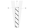
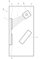
- FIG. 8 is a schematic diagram showing an outline of a sputtering apparatus for forming an inorganic material layer in this step.
- the sputtering apparatus 100 includes a particle beam source 6 and a sputtering target 5 in a chamber 8 that forms a space isolated from the atmosphere.
- the particle beam source 6 is rotatably supported by a rotation shaft 6a, and is configured so that the particle beam B can scan the entire surface of the sputtering target 5.
- the polymer film 2 is placed vertically in the chamber 8.
- atoms or clusters M of an inorganic material are generated from the sputtering target 5.
- the generated atoms or clusters M of the inorganic material are irradiated on both sides of the polymer film 2, and the inorganic material layer 4 is formed on both sides of the polymer film 2 (FIGS. 2 and 3).
- the inorganic material layer 4 is formed by the ion beam sputtering method using metal or Si as the sputtering target 5.
- the method is not limited to this, and the method for forming the inorganic material layer 4 may be appropriately selected depending on the desired characteristics of the polymer film laminate 1, such as the ALD method, the magnetron sputtering method, and the CVD method.
- the sputtering target 5 one containing any one of aluminum (Al), titanium (Ti), nickel (Ni), and silicon (Si) as a main component may be adopted.
- transition metals such as tantalum (Ta), chromium (Cr), gold (Au) and platinum (Pt), solder alloys containing tin (Sn) and silver (Ag), copper (Cu), iron (Fe) and the like. May be adopted.
- the particle beam B is irradiated with energy particles of a mixed gas composed of an inert gas and an oxygen gas, but other configurations include rare gas such as argon (Ar) and xenone (Xe), nitrogen, and the like. Oxygen or a mixed gas thereof can also be adopted.
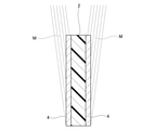
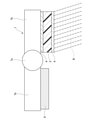
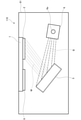
- the joining device 110 includes a bonding device 7 arranged above the chamber 8, a particle beam source 6, and a sputtering target 5 in a chamber 81 that forms a space isolated from the atmosphere.
- the particle beam source 6 is rotatably supported by the rotation shaft 6a, and the particle beam B irradiated from the particle beam source 6 can scan the surfaces of the polymer film 2 and the copper foil 9 held by the bonding device 7. It is configured as follows. Further, as shown in FIG. 10, the particle beam source 6 is configured so that the particle beam B can scan the surface of the sputtering target 5.
- the atoms or clusters M of the inorganic material generated by the particle beam B scanning the sputter target 5 are configured to irradiate the surfaces of the polymer film 2 and the copper foil 9 held in the bonding device 7. ..
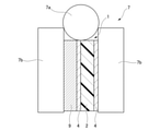
- FIG. 4 is a schematic diagram for explaining the joining process of the present embodiment including an enlarged view of the bonding device 7.
- the laminating device 7 arranged on the upper part of the joining device 110 includes a holding plate 7b extending to the left and right from the rotating shaft 7a rotatably supported via the rotating shaft 7a.
- the first polymer film 2 and the copper foil 9 on which the inorganic material layers 4 are formed on both sides in the above-mentioned inorganic material layer forming step are held.
- the particle beam B irradiates the surface of the inorganic material layer 4 formed on the lower side of the polymer film 2, and particles having a predetermined kinetic energy are applied to the surface of the inorganic material layer 4. The collision occurs and the surface of the planned joining surface is activated.
- the left and right holding plates 7b of the bonding device 7 are folded downward together with the polymer film 2 and the copper foil 9 about the rotation axis 7a as the rotation center, and as shown in FIG.
- the polymer film 2 having the inorganic material layer 4 formed on both sides thereof and the copper foil 9 are joined.
- heating is performed by an electric heater (not shown) embedded in the holding plate 7b. The heating is preferably performed at 350 ° C. or lower.
- the polymer film laminate 1 is taken out, and the manufacturing process of the polymer film laminate 1 shown in FIG. 1 is completed.
- the polymer film 2 adopted is LCP (liquid crystal polymer), PFA (tetrafluoroethylene / perfluoroalkyl vinyl ether copolymer), polyimide (polytetrafluoroethylene), PPS (polyphenylene sulfide), and the like.
- PI-based including PI (polyimide), MPI (modified polyimide)
- PPE-based including PPE (polyphenylene ether), mPPE (modified polyphenylene ether)
- cycloolefin polymer scroolefin copolymer, polystyrene, syndiotactic polystyrene , Polyethylene naphthalate, polyethylene, polypropylene, polyethylene terephthalate, polyethylene naphthalate, polyamide, vinyl chloride resin, polystyrene, acrylic, polycarbonate, polyether ether ketone, polyether sulfone, aramid, ethylene / ethylene tetrafluoride copolymer resin, It is a laminate of any one or a combination of a tetrafluoride ethylene / fluorinated propylene copolymer resin, polyarylate, polyetherimide, polyamideimide, thermoplastic polyimide, maleimide resin
- the steps from the formation of the inorganic material layer 4 to the joining are performed in a vacuum.
- the degree of vacuum before the start of the process reaches a pressure of 1 ⁇ 10 -5 Pa (Pascal) or less.
- the present invention is not limited to this, and the process may be carried out in an inert gas or at atmospheric pressure while ensuring a clean environment.
- a polymer film laminate 1 provided with a copper foil 9 is prepared.
- D) The photoresist layer p covered with the photomask m having a wiring pattern is irradiated with UV light u to form a cured portion pc on the photoresist layer p.
- the inorganic material layer 4 is made of the polymer film 2 and copper. It can be used in a dual role of a role as an adhesive layer of the foil 4 and a role as a stopper layer for etching the copper foil 4.
- FIG. 11 is an enlarged view of the surface of the substrate 1A provided with the copper foil in the prior art.
- the surface of the copper foil 9A toward the adhesive layer 4A and the surface of the substrate 2A toward the adhesive layer 4A in the prior art are on the surface in order to increase the surface area and secure the adhesion strength by utilizing the anchor effect.
- a few um of "roughening” is applied. Therefore, due to the influence of "roughening of the surface", the electric signal j0 is transmitted along the unevenness thereof, the moving distance becomes long, and the loss becomes large. Further, the unevenness causes a place where the electric field strength is high, and the leakage current r0 tends to increase.
- FIG. 12 is an enlarged view of the surface of the polymer film laminate 1 in the present embodiment.
- the copper foil 9 and the polymer film 2 are bonded via the inorganic material layer 4, so that the copper foil 9 and the inorganic material layer 4 (adhesive layer 4A in the conventional example) are bonded to each other.
- Boundary K has a smooth surface.
- the electric signal j1 is transmitted along the smooth surface thereof, and the traveling distance is shortened and the loss can be reduced as compared with the conventional technique. Further, due to the smooth surface, the electric field strength becomes relatively uniform and the leakage current r1 can be reduced.
- LCP liquid crystal polymer
- PFA tetrafluoroethylene / perfluoroalkyl vinyl ether copolymer
- polyimide polytetrafluoroethylene
- PPS polyphenylene sulfide
- PI-based including PI (polyimide), MPI (modified polyimide)
- PPE-based including PPE (polyphenylene ether), mPPE (modified polyphenylene ether)
- cycloolefin polymer scroolefin copolymer, polystyrene, syndiotac Tick polystyrene, polyethylene naphthalate, polyethylene, polypropylene, polyethylene terephthalate, polyethylene naphthalate, polyamide, vinyl chloride resin, polystyrene, acrylic, polycarbonate, polyether ether ketone, polyether sulfone, aramid, ethylene / ethylene tetrafluoride copolymer
- the polymer film 2 is bonded to the copper foil 9 via the inorganic material layer 4, the polymer film and the copper foil can be bonded to the copper foil 9 firmly at a low temperature, which can be used in a high frequency circuit.
- the method and the polymer film laminate can be provided at low cost.
- the inorganic material layers 4 are formed on both surfaces of the polymer film 2, it is possible to provide the polymer film laminate 1 having excellent moisture resistance.
- a copper foil having a thickness of 6 ⁇ m to 38 ⁇ m is used to form the polymer film laminate 1.
- the polymer laminate 1 has a gas permeability of 1E-03cc / m 2 ⁇ day to 1E-01cc / m 2 ⁇ day, a conductivity of 1E + 13 ⁇ ⁇ cm to 1E + 18 ⁇ ⁇ cm, and a dielectric constant of 2.0 to 3. 5.
- the dielectric loss tangent is 0.0002 to 0.003.
- the present invention provides a polymer laminate 1 that can be used in a high frequency circuit so that the gas (oxygen) permeability is reduced (improved) by the intervention of an inorganic layer and the dielectric constant and conductivity (insulation) are not deteriorated. can do.
- the inorganic material layer 4 is formed on both sides of the polymer film 2, but a surface activation treatment is performed in which particles having a predetermined kinetic energy are made to collide with the surface to be formed of the inorganic material layer before the formation. You may go.
- the inorganic material layer 4 may be formed from a plurality of layers. Any one of an ion beam sputtering method, an ALD method, and a magnetron sputtering method may be adopted for forming each of the plurality of layers of the inorganic material. Further, the inorganic material layer 4 is formed on the entire surface of the polymer film 2, but is not limited to this, and the inorganic material layer 4 may be formed on a part of the surface of the polymer film 2.
- FIG. 6 shows the polymer film laminate 20 according to the second embodiment of the present invention.
- This embodiment differs from the first embodiment in the configuration of the polymer film laminate 20.
- the inorganic material layer 4 is formed on one side of the polymer film 2.
- the surface activation treatment shown in FIG. 9 is performed on the planned formation surface of the inorganic material layer 4 of the polymer film 2. Since other configurations and operations are the same as those of the first embodiment, the description thereof will be omitted here.
- the process can be simplified and the cost can be reduced as compared with the first embodiment.
- FIG. 7 shows the polymer film laminate 30 according to the third embodiment of the present invention.
- This embodiment differs from the first embodiment in the configuration of the polymer film laminate 30.
- the inorganic material layers 4a and 4b formed on both sides of the polymer film 2 are composed of two layers, a first inorganic material layer 4a and a second inorganic material layer 4b.
- the first inorganic material layer 4a is formed by the ALD method
- the second inorganic material layer 4b is formed by the ion beam sputtering method. Since other configurations and operations are the same as those of the first embodiment, the description thereof will be omitted here.
- the inorganic material layers 4a and 4b formed on both sides of the polymer film 2 are the first inorganic material layer 4a and the second inorganic material layer 4b. Since it is composed of two layers, the bonding strength and moisture resistance are further improved.
- the first inorganic material layer is composed of a Si and oxygen-containing film
- the second inorganic material layer is composed of a Ti-containing film.
- the second inorganic material layer is a Cu-etched stopper film
- the first inorganic material layer Si and oxygen-containing film
- the inorganic material layer 4 formed of these plurality of layers can adopt a configuration in consideration of not only the function as an adhesive layer but also various plurality of roles. Although the two layers of the inorganic material have been described here, the present invention is not limited to this, and any number of layers may be formed. Further, when considering a film having low conductivity, an Al and oxygen-containing film may be adopted instead of the Si and oxygen-containing film described above.
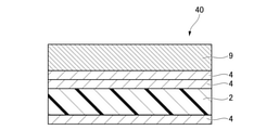
- FIG. 14 shows the polymer film laminate 40 according to the fourth embodiment of the present invention. This embodiment differs from the first embodiment in the configuration of the polymer film laminate 30.
- the inorganic material layer 4 is also formed on the joint surface of the copper foil 9.
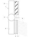
- FIG. 15 shows a state in which the copper foil 9 and the polymer film 2 having the inorganic material layers 4 formed on both sides thereof are held by the holding plate 7b of the bonding device 7.
- the particle beam source 6 is configured so that the particle beam B can scan the surface of the sputtering target 5, and the atoms or clusters M of the inorganic material generated thereby are held by the bonding device 7.
- the surface of the copper foil 9 is irradiated with atoms or clusters M of an inorganic material, and the inorganic material layer 4 is formed on the planned bonding surface of the copper foil 9 before bonding. Since other configurations and operations are the same as those of the first embodiment, the description thereof will be omitted here.
- the inorganic material layer 4 is formed on the planned joining surface of the copper foil 9, so that the joining strength and the moisture resistance are further improved.
Landscapes
- Engineering & Computer Science (AREA)
- Microelectronics & Electronic Packaging (AREA)
- Laminated Bodies (AREA)
Priority Applications (1)
| Application Number | Priority Date | Filing Date | Title |
|---|---|---|---|
| JP2022543295A JPWO2022038876A1 (https=) | 2020-08-20 | 2021-06-14 |
Applications Claiming Priority (2)
| Application Number | Priority Date | Filing Date | Title |
|---|---|---|---|
| JP2020139040 | 2020-08-20 | ||
| JP2020-139040 | 2020-08-20 |
Publications (1)
| Publication Number | Publication Date |
|---|---|
| WO2022038876A1 true WO2022038876A1 (ja) | 2022-02-24 |
Family
ID=80323587
Family Applications (1)
| Application Number | Title | Priority Date | Filing Date |
|---|---|---|---|
| PCT/JP2021/022432 Ceased WO2022038876A1 (ja) | 2020-08-20 | 2021-06-14 | 高分子フィルムと銅箔の接合方法、高分子フィルム積層体および高分子フィルム積層体を備えるデバイス |
Country Status (3)
| Country | Link |
|---|---|
| JP (1) | JPWO2022038876A1 (https=) |
| TW (1) | TW202208161A (https=) |
| WO (1) | WO2022038876A1 (https=) |
Cited By (1)
| Publication number | Priority date | Publication date | Assignee | Title |
|---|---|---|---|---|
| CN117328062A (zh) * | 2023-08-18 | 2024-01-02 | 基迈克材料科技(苏州)有限公司 | 一种增强锂电池复合集流体膜基结合力的方法 |
Citations (4)
| Publication number | Priority date | Publication date | Assignee | Title |
|---|---|---|---|---|
| JP2006245303A (ja) * | 2005-03-03 | 2006-09-14 | Nikko Kinzoku Kk | 銅箔の表面処理方法 |
| JP2006310357A (ja) * | 2005-04-26 | 2006-11-09 | Teijin Ltd | フレキシブルプリント回路用基板 |
| JP2009073943A (ja) * | 2007-09-20 | 2009-04-09 | Seiko Epson Corp | 接合方法および接合体 |
| JP2011009453A (ja) * | 2009-06-25 | 2011-01-13 | Jx Nippon Mining & Metals Corp | プリント配線板用銅箔 |
Family Cites Families (1)
| Publication number | Priority date | Publication date | Assignee | Title |
|---|---|---|---|---|
| CN104245280B (zh) * | 2012-04-10 | 2017-03-29 | 须贺唯知 | 接合高分子薄膜与高分子薄膜的方法、接合高分子薄膜与无机材料基板的方法、高分子薄膜层叠体及高分子薄膜与无机材料基板的层叠体 |
-
2021
- 2021-06-14 WO PCT/JP2021/022432 patent/WO2022038876A1/ja not_active Ceased
- 2021-06-14 JP JP2022543295A patent/JPWO2022038876A1/ja active Pending
- 2021-08-17 TW TW110130289A patent/TW202208161A/zh unknown
Patent Citations (4)
| Publication number | Priority date | Publication date | Assignee | Title |
|---|---|---|---|---|
| JP2006245303A (ja) * | 2005-03-03 | 2006-09-14 | Nikko Kinzoku Kk | 銅箔の表面処理方法 |
| JP2006310357A (ja) * | 2005-04-26 | 2006-11-09 | Teijin Ltd | フレキシブルプリント回路用基板 |
| JP2009073943A (ja) * | 2007-09-20 | 2009-04-09 | Seiko Epson Corp | 接合方法および接合体 |
| JP2011009453A (ja) * | 2009-06-25 | 2011-01-13 | Jx Nippon Mining & Metals Corp | プリント配線板用銅箔 |
Cited By (1)
| Publication number | Priority date | Publication date | Assignee | Title |
|---|---|---|---|---|
| CN117328062A (zh) * | 2023-08-18 | 2024-01-02 | 基迈克材料科技(苏州)有限公司 | 一种增强锂电池复合集流体膜基结合力的方法 |
Also Published As
| Publication number | Publication date |
|---|---|
| JPWO2022038876A1 (https=) | 2022-02-24 |
| TW202208161A (zh) | 2022-03-01 |
Similar Documents
| Publication | Publication Date | Title |
|---|---|---|
| CN112601370B (zh) | 覆铜积层板及覆铜积层板的制造方法 | |
| JP4971460B2 (ja) | フレキシブル配線板及びその製造方法 | |
| CN103181247A (zh) | 高频电路基板 | |
| WO2002089161A1 (en) | Capacitor and its manufacturing method | |
| CN101431857A (zh) | 印制线路板 | |
| JP2006190928A (ja) | Bgaパッケージおよびその製造方法 | |
| WO2010103941A1 (ja) | フレキシブル基板 | |
| CN102612256A (zh) | 配线部件及其制造方法 | |
| WO2022038876A1 (ja) | 高分子フィルムと銅箔の接合方法、高分子フィルム積層体および高分子フィルム積層体を備えるデバイス | |
| JP2012244056A (ja) | フッ素樹脂基板の製造方法 | |
| WO2022038875A1 (ja) | 高分子フィルム積層体の製造方法、高分子フィルム積層体および高分子フィルム積層体を備えるデバイス | |
| JP2004082444A (ja) | 金属層付き樹脂体および配線体 | |
| JP2005324511A (ja) | 積層体及びその製造方法 | |
| JP2002252436A (ja) | 両面積層板およびその製造方法 | |
| JP2022039457A (ja) | 回路基板及びその製造方法 | |
| JP2023003106A (ja) | 複層シート及びその製造方法 | |
| WO2003032701A1 (en) | Method for manufacturing multilayer wiring board, and multilayer wiring board manufactured by the same | |
| JPH0644667B2 (ja) | シ−ルド付可撓性プリント回路基板 | |
| JP7677394B2 (ja) | フレキシブル基板の製造方法 | |
| JP2006156576A (ja) | リジッドフレックス多層プリント配線板の製造方法 | |
| TW202521346A (zh) | 導電性膜及其製造方法 | |
| JP2007081274A (ja) | フレキシブル回路用基板 | |
| JP2013157566A (ja) | プリント配線板及び該プリント配線板の製造方法 | |
| JP2004342978A (ja) | マルチワイヤ配線板の製造方法 | |
| JP2008290424A (ja) | フレキシブル基材 |
Legal Events
| Date | Code | Title | Description |
|---|---|---|---|
| 121 | Ep: the epo has been informed by wipo that ep was designated in this application |
Ref document number: 21858027 Country of ref document: EP Kind code of ref document: A1 |
|
| ENP | Entry into the national phase |
Ref document number: 2022543295 Country of ref document: JP Kind code of ref document: A |
|
| NENP | Non-entry into the national phase |
Ref country code: DE |
|
| 122 | Ep: pct application non-entry in european phase |
Ref document number: 21858027 Country of ref document: EP Kind code of ref document: A1 |