WO2022034636A1 - 炭化珪素半導体装置および電力変換装置 - Google Patents
炭化珪素半導体装置および電力変換装置 Download PDFInfo
- Publication number
- WO2022034636A1 WO2022034636A1 PCT/JP2020/030578 JP2020030578W WO2022034636A1 WO 2022034636 A1 WO2022034636 A1 WO 2022034636A1 JP 2020030578 W JP2020030578 W JP 2020030578W WO 2022034636 A1 WO2022034636 A1 WO 2022034636A1
- Authority
- WO
- WIPO (PCT)
- Prior art keywords
- region
- silicon carbide
- semiconductor device
- well
- layer
- Prior art date
- Legal status (The legal status is an assumption and is not a legal conclusion. Google has not performed a legal analysis and makes no representation as to the accuracy of the status listed.)
- Ceased
Links
Images








Classifications
-
- H—ELECTRICITY
- H10—SEMICONDUCTOR DEVICES; ELECTRIC SOLID-STATE DEVICES NOT OTHERWISE PROVIDED FOR
- H10D—INORGANIC ELECTRIC SEMICONDUCTOR DEVICES
- H10D30/00—Field-effect transistors [FET]
- H10D30/60—Insulated-gate field-effect transistors [IGFET]
- H10D30/64—Double-diffused metal-oxide semiconductor [DMOS] FETs
- H10D30/66—Vertical DMOS [VDMOS] FETs
- H10D30/665—Vertical DMOS [VDMOS] FETs having edge termination structures
-
- H—ELECTRICITY
- H10—SEMICONDUCTOR DEVICES; ELECTRIC SOLID-STATE DEVICES NOT OTHERWISE PROVIDED FOR
- H10D—INORGANIC ELECTRIC SEMICONDUCTOR DEVICES
- H10D12/00—Bipolar devices controlled by the field effect, e.g. insulated-gate bipolar transistors [IGBT]
- H10D12/01—Manufacture or treatment
- H10D12/031—Manufacture or treatment of IGBTs
-
- H—ELECTRICITY
- H10—SEMICONDUCTOR DEVICES; ELECTRIC SOLID-STATE DEVICES NOT OTHERWISE PROVIDED FOR
- H10D—INORGANIC ELECTRIC SEMICONDUCTOR DEVICES
- H10D30/00—Field-effect transistors [FET]
- H10D30/01—Manufacture or treatment
- H10D30/021—Manufacture or treatment of FETs having insulated gates [IGFET]
- H10D30/028—Manufacture or treatment of FETs having insulated gates [IGFET] of double-diffused metal oxide semiconductor [DMOS] FETs
- H10D30/0291—Manufacture or treatment of FETs having insulated gates [IGFET] of double-diffused metal oxide semiconductor [DMOS] FETs of vertical DMOS [VDMOS] FETs
-
- H—ELECTRICITY
- H10—SEMICONDUCTOR DEVICES; ELECTRIC SOLID-STATE DEVICES NOT OTHERWISE PROVIDED FOR
- H10D—INORGANIC ELECTRIC SEMICONDUCTOR DEVICES
- H10D62/00—Semiconductor bodies, or regions thereof, of devices having potential barriers
- H10D62/10—Shapes, relative sizes or dispositions of the regions of the semiconductor bodies; Shapes of the semiconductor bodies
- H10D62/102—Constructional design considerations for preventing surface leakage or controlling electric field concentration
- H10D62/103—Constructional design considerations for preventing surface leakage or controlling electric field concentration for increasing or controlling the breakdown voltage of reverse-biased devices
- H10D62/105—Constructional design considerations for preventing surface leakage or controlling electric field concentration for increasing or controlling the breakdown voltage of reverse-biased devices by having particular doping profiles, shapes or arrangements of PN junctions; by having supplementary regions, e.g. junction termination extension [JTE]
- H10D62/106—Constructional design considerations for preventing surface leakage or controlling electric field concentration for increasing or controlling the breakdown voltage of reverse-biased devices by having particular doping profiles, shapes or arrangements of PN junctions; by having supplementary regions, e.g. junction termination extension [JTE] having supplementary regions doped oppositely to or in rectifying contact with regions of the semiconductor bodies, e.g. guard rings with PN or Schottky junctions
-
- H—ELECTRICITY
- H10—SEMICONDUCTOR DEVICES; ELECTRIC SOLID-STATE DEVICES NOT OTHERWISE PROVIDED FOR
- H10D—INORGANIC ELECTRIC SEMICONDUCTOR DEVICES
- H10D62/00—Semiconductor bodies, or regions thereof, of devices having potential barriers
- H10D62/10—Shapes, relative sizes or dispositions of the regions of the semiconductor bodies; Shapes of the semiconductor bodies
- H10D62/124—Shapes, relative sizes or dispositions of the regions of semiconductor bodies or of junctions between the regions
- H10D62/126—Top-view geometrical layouts of the regions or the junctions
- H10D62/127—Top-view geometrical layouts of the regions or the junctions of cellular field-effect devices, e.g. multicellular DMOS transistors or IGBTs
-
- H—ELECTRICITY
- H10—SEMICONDUCTOR DEVICES; ELECTRIC SOLID-STATE DEVICES NOT OTHERWISE PROVIDED FOR
- H10D—INORGANIC ELECTRIC SEMICONDUCTOR DEVICES
- H10D62/00—Semiconductor bodies, or regions thereof, of devices having potential barriers
- H10D62/80—Semiconductor bodies, or regions thereof, of devices having potential barriers characterised by the materials
- H10D62/83—Semiconductor bodies, or regions thereof, of devices having potential barriers characterised by the materials being Group IV materials, e.g. B-doped Si or undoped Ge
- H10D62/832—Semiconductor bodies, or regions thereof, of devices having potential barriers characterised by the materials being Group IV materials, e.g. B-doped Si or undoped Ge being Group IV materials comprising two or more elements, e.g. SiGe
- H10D62/8325—Silicon carbide
Definitions
- the present disclosure relates to a silicon carbide semiconductor device and a power conversion device, and more particularly to a silicon carbide semiconductor device having an ohmic electrode and a power conversion device having the same.
- the SiC semiconductor device typically has a single crystal SiC substrate and a SiC layer which is an epitaxial layer formed on the single crystal SiC substrate. If the device includes a pn diode configuration, continued flow of forward or bipolar currents through the pn diode may result in stacking defects in the crystals of the SiC layer. This is due to the recombination energy when the minority carriers injected through the pn junction of the pn diode recombine with the majority carriers, starting from the basal plane dislocation (BPD) existing in the SiC substrate and the like. It is believed that this is because the stacking defects, which are defects, expand in the SiC layer. Expansion of stacking defects causes characteristic deterioration such as an increase in forward voltage (on-voltage) due to obstruction of current flow and a decrease in withstand voltage.
- BPD basal plane dislocation
- the above-mentioned characteristic deterioration can occur not only when the semiconductor device is a simple pn diode but also when it is a vertical MOSFET (Metal Oxide Semiconductor Field Effect Transistor). This is because the vertical MOSFET has a built-in body diode (parasitic diode) between the source and drain, which is a kind of pn diode. Specifically, the above-mentioned deterioration of characteristics occurs when a body diode functions as a freewheeling diode of a MOSFET in a power electronics system, and a forward current flows through the body diode.
- a body diode functions as a freewheeling diode of a MOSFET in a power electronics system
- a SiC-PWM and a SiC-Schottky barrier diode have an epitaxial layer grown on a SiC substrate. Used as a pressure resistant holding layer.
- a large number of defects are usually present in a SiC substrate, and these defects also include defects that are the starting points for expansion of laminated defects in the epitaxial layer. Therefore, in order to improve the quality of the epitaxial layer growing on the SiC substrate, attempts have been made for many years to detoxify various defects.
- the following three methods have been mainly studied so far as methods for suppressing the above-mentioned characteristic deterioration caused by the flow of forward current through the body diode.
- a first method when the epitaxial layer is grown on the SiC substrate, the basal plane dislocations inherited from the SiC substrate to the epitaxial layer are converted from the basal plane dislocations to the through-blade dislocations in the initial stage of growth.
- a method for preventing the expansion of stacking defects from surface dislocations has been studied (see, for example, Non-Patent Document 1).
- the second method is to prevent the occurrence of stacking defects from dislocations of the basal plane of the SiC substrate by promoting recombination of holes and electrons by a buffer layer having a high impurity concentration formed on the SiC substrate. It has been studied (see, for example, Non-Patent Document 2). As a third method, the recombination center is introduced in the region where the parasitic pn diode is provided to reduce the injected holes, whereby the holes and electrons in the vicinity of the dislocation of the basal plane of the SiC substrate are transferred. A method for preventing recombination has been studied (see, for example, Patent Document 2).
- the present inventors have noticed that none of the above-mentioned conventional methods has sufficiently examined the difference in bipolar current density in a semiconductor chip as a SiC semiconductor device. Specifically, the present inventors have found that the bipolar current density is locally increased in a local region near the boundary between the active region and the outer peripheral region of the chip. By studying the influence of such a bipolar current density distribution, the expansion of stacking defects can be suppressed in most regions of the chip by simply applying the above-mentioned conventional method. The present inventors have conceived that it may not be sufficiently suppressed in the above-mentioned local region. Hereinafter, this problem will be described more specifically.
- the recombination center is usually a defect such as a point defect, the presence of an excessive recombination center causes a decrease in withstand voltage, an increase in on-voltage, and an increase in leakage current. It ends up.
- the present disclosure has been made to solve the above problems, and an object thereof is to provide a silicon carbide semiconductor device capable of suppressing deterioration of characteristics while avoiding a significant increase in manufacturing cost. ..
- the silicon carbide semiconductor device includes a silicon carbide substrate, a silicon carbide layer, a gate insulating film, a gate electrode, a gate pad, a source electrode, and a plurality of ohmic electrodes. ing.
- the silicon carbide substrate has a first conductive type.
- the silicon carbide layer has a first surface facing the silicon carbide substrate and a second surface opposite to the first surface in the thickness direction, and the active region and the active region in the in-plane direction perpendicular to the thickness direction. It has an outer peripheral area arranged on the outer circumference.
- the silicon carbide layer includes a drift layer, a plurality of first well regions, a plurality of source regions, and a second well region.
- the drift layer is arranged on a silicon carbide substrate and has a first conductive type.
- the plurality of first well regions are arranged on the drift layer in the active region, have a second conductive type different from the first conductive type, and are separated from each other in at least one cross-sectional view.
- the plurality of source regions are arranged on the plurality of first well regions and have a first conductive type.
- the second well region is arranged on the drift layer in the outer peripheral region and has a second conductive type.
- the gate insulating film faces a plurality of first well regions.
- the gate electrode has a portion arranged above the active region and facing a plurality of first well regions via a gate insulating film, and a portion arranged above the outer peripheral region and insulated from the second well region.
- the gate pad is located above the second well region, is isolated from the second well region, and is connected to the gate electrode.
- the source electrode is provided above the second surface of the silicon carbide layer.
- the plurality of ohmic electrodes are provided on the second surface of the silicon carbide layer, are connected to the source electrode, and are electrically ohmicly connected to the plurality of first well regions, and are connected to the first well region of the silicon carbide layer. It has a plurality of surface regions that make ohmic contact with the portion of the two surfaces having the second conductive mold.
- the active region includes a standard region portion and a thinning region portion between the standard region portion and the outer peripheral region. The area density of the plurality of surface areas in the plan view is lower in the thinned area portion than in the standard region portion.
- the silicon carbide semiconductor device includes a silicon carbide substrate, a silicon carbide layer, a gate insulating film, a gate electrode, a gate pad, a source electrode, and a plurality of ohmic electrodes. ing.
- the silicon carbide substrate has a first conductive type.
- the silicon carbide layer has a first surface facing the silicon carbide substrate and a second surface opposite to the first surface in the thickness direction, and the active region and the active region in the in-plane direction perpendicular to the thickness direction. It has an outer peripheral area arranged on the outer circumference.
- the silicon carbide layer includes a drift layer, a plurality of first well regions, a plurality of source regions, and a second well region.
- the drift layer is arranged on a silicon carbide substrate and has a first conductive type.
- the plurality of first well regions are arranged on the drift layer in the active region, have a second conductive type different from the first conductive type, and are separated from each other in at least one cross-sectional view.
- the plurality of source regions are arranged on the plurality of first well regions and have a first conductive type.
- the second well region is arranged on the drift layer in the outer peripheral region and has a second conductive type.
- the gate insulating film faces a plurality of first well regions.
- the gate electrode has a portion arranged above the active region and facing a plurality of first well regions via a gate insulating film, and a portion arranged above the outer peripheral region and insulated from the second well region.
- the gate pad is located above the second well region, is isolated from the second well region, and is connected to the gate electrode.
- the source electrode is provided above the second surface of the silicon carbide layer.
- the plurality of ohmic electrodes are provided on the second surface of the silicon carbide layer, are connected to the source electrode, and are electrically ohmicly connected to the plurality of first well regions and second well regions. It has a plurality of surface regions that make ohmic contact with the portion of the second surface of the silicon carbide layer having the second conductive type.
- the outer peripheral region includes an outer region portion and a thinning region portion between the outer region portion and the active region. The area density of the plurality of surface regions in the plan view is lower in the thinned region portion than in the active region.
- FIG. 2 is a partial cross-sectional view schematically showing the configuration of a silicon carbide semiconductor device along lines III-III in FIG. 2.
- a first well region, a second well region, a portion of the upper surface of the silicon carbide layer having the second conductive type, and a plurality of surface regions in which a plurality of ohmic electrodes are in ohmic contact are formed.
- a partial top view which shows roughly.
- FIG. 5 is a cross-sectional view showing the configuration of a pn diode used in a simulation of a current density distribution (FIGS. 8 and 9) and a hole concentration distribution (FIG. 10) in a reflux operation, corresponding to a comparative example. It is a distribution map which shows the simulation result of the current density distribution in the configuration of the pn diode shown in FIG. 7 corresponding to the comparative example.
- FIG. 11 at the depth position of the bottom surface of the drift layer. It is a partial top view which shows the 1st modification of the structure shown in FIG. It is a partial top view which shows the 2nd modification of the structure shown in FIG. It is a partial top view which shows the 3rd modification of the structure shown in FIG. It is a partial top view which shows the 4th modification of the structure shown in FIG.
- the first well region, the second well region, the portion of the upper surface of the silicon carbide layer having the second conductive type, and the plurality of ohmic electrodes are in ohmic contact.
- FIG. 3 is a partial top view schematically showing a plurality of surface regions with the same field of view as in FIG. It is a block diagram which shows the structure of the power conversion system to which the power conversion apparatus which concerns on this Embodiment 3 is applied.
- an n-channel MOSFET that is, a MOSFET in which the first conductive type is n-type and the second conductive type is p-type is an example. It will be explained by listing in. The description of the high and low potentials in the above description is for the case where the first conductive type is n type and the second conductive type is p type, and the first conductor is p type and the second conductive type is p type. In the case of n-type, the high and low potentials are reversed.
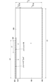
- FIG. 1 is a top view schematically showing the configuration of the MOSFET 711 (silicon carbide semiconductor device) according to the first embodiment.
- the MOSFET 711 has a source electrode 80, a gate pad 81, and a gate wiring 82 on the upper surface thereof.
- the gate wiring 82 extends from the gate pad 81, and the source electrode 80 is arranged away from the gate pad 81.
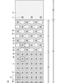
- FIG. 2 is a partial top view schematically showing the configuration of the silicon carbide layer SL (FIG. 3) included in the MOSFET 711 in the broken line portion II in FIG. 1.
- FIG. 3 is a partial cross-sectional view schematically showing the configuration of MOSFET 711 along lines III-III in FIG.
- the MOSFET 711 includes a silicon carbide substrate 10 (hereinafter, also referred to as SiC substrate 10), a silicon carbide layer SL (hereinafter, also referred to as SiC layer SL), a gate insulating film 50, a gate electrode 60, a gate pad 81, and a source. It has an electrode 80, a plurality of ohmic electrodes 70, and a drain electrode 84.
- the SiC substrate 10 has an n-type (first conductive type).
- the SiC layer SL has a lower surface (first surface) facing the SiC substrate 10 and an upper surface (second surface opposite to the first surface in the thickness direction). The lower surface of the SiC layer SL may be in contact with the SiC substrate 10.
- the SiC layer SL has an active region 100 and an outer peripheral region 200 arranged on the outer periphery of the active region 100 in the in-plane direction perpendicular to the thickness direction. Typically, in the in-plane direction (in other words, in a plan view), the outer peripheral region 200 surrounds the active region 100.
- the active region 100 directly bears the main function of the MOSFET 711, that is, the function of switching the current. Therefore, the MOS gate structure of the MOSFET 711 is arranged not in the outer peripheral region 200 but in the active region 100.
- the SiC layer SL includes a drift layer 20, a plurality of first well regions 30, a plurality of source regions 40, a second well region 31, a contact region 35, and a JTE (Junction Termination Extension) region 37. And include.
- the drift layer 20 has an n-type.
- the impurity concentration of the drift layer 20 is lower than the impurity concentration of the SiC substrate 10.
- the drift layer 20 is arranged on the SiC substrate 10.
- the first well region 30 has a p-type (a second conductive type different from the first conductive type).
- the first well region 30 is arranged on the drift layer 20 in the active region 100 and typically partially forms the upper surface of the SiC layer SL.
- the first well regions 30 are separated from each other in at least one cross-sectional view (eg, the cross-sectional view shown in FIG. 3).
- the drift layer 20 has a JFET region 21 between two adjacent first well regions 30.
- the impurity concentration of the JFET region 21 which is a part of the drift layer 20 may be the same as or different from the impurity concentration of the other part of the drift layer 20.
- the source area 40 has an n type.
- the source region 40 is arranged on the plurality of first well regions 30.
- the source region 40 is separated from the drift layer 20 by a first well region 30.
- the outer edge of each source region 40 is arranged inside the outer edge of each first well region 30 on the upper surface of the silicon carbide layer SL, whereby the upper surface of the silicon carbide layer SL is arranged.
- each source region 40 is separated from the drift layer 20 by a first well region 30.
- the contact region 35 has a p-type and has an impurity concentration higher than that of the first well region 30.
- the contact region 35 has an upper end reaching the upper surface of the SiC layer SL and a lower end reaching the first well region 30.
- the contact region 35 is surrounded by the source region 40 in plan view.
- the second well region 31 has a p-type.
- the second well region 31 typically partially forms the upper surface of the SiC layer SL.
- the second well region 31 is typically larger than each of the first well regions 30.
- the second well region 31 is arranged on the drift layer 20 in the outer peripheral region 200. Specifically, the second well region 31 is arranged outside the outermost first well region 30 via the JFET region 21. Although the second well region 31 is separated from the first well region 30 in the first embodiment, it may be connected to the first well region 30 as a modification (see, for example, FIG. 13). ..
- a plurality of ohmic electrodes 70 are provided on the upper surface of the SiC layer SL.
- the ohmic electrode 70 in the active region 100 is in ohmic contact with the source region 40 and the contact region 35 reaching the first well region 30.
- the ohmic electrode 70 in the outer peripheral region 200 is in ohmic contact with the contact region 35 reaching the second well region 31.
- the plurality of ohmic electrodes 70 are electrically ohmicly connected to the plurality of first well regions 30 and second well regions 31.
- the plurality of ohmic electrodes 70 have a plurality of portions that make ohmic contact with the portion of the upper surface of the SiC layer having an n-type (specifically, the source region 40) and the p-type of the upper surface of the SiC layer. It has a plurality of portions that make ohmic contact with the portion (specifically, the contact region 35), and in particular, the latter is also referred to as a plurality of surface regions in the following. According to this definition, each of the plurality of surface regions is a boundary surface between the portion of the upper surface of the SiC layer having a p-shape and the ohmic electrode 70.
- the material of the ohmic electrode 70 is selected so that electrons and holes can be easily transferred to and from the source region 40 and the contact region 35, both of which have relatively high impurity concentrations.
- This material is typically a silicide alloy, for example a nickel silicide alloy.
- the gate insulating film 50 has at least a portion facing a plurality of first well regions 30.
- the gate insulating film 50 covers the portion straddling the boundary between the source region 40 and the first well region 30 and the first well region 30 between the boundary and the JFET region 21.
- the gate insulating film 50 may further have a portion facing the second well region 31.
- the gate electrode 60 is arranged above the active region 100 and faces a plurality of first well regions 30 via the gate insulating film 50, and is arranged above the outer peripheral region 200 and insulated from the second well region 31. It has a part and. Of the first well region 30, the surface layer facing the gate electrode 60 via the gate insulating film 50 has a function as a channel region.
- the gate electrode 60 extends from the active region 100 into the outer peripheral region 200.
- the interlayer insulating film 55 covers the gate electrode 60.
- the gate electrode 60 is connected to the gate wiring 82 via the contact hole 95 of the interlayer insulating film 55 while being insulated from the second well region 31 by the gate insulating film 50 and the field insulating film 51.
- the field insulating film 51 is provided on the outer peripheral region 200.
- the thickness of the field insulating film 51 is larger than the thickness of the gate insulating film 50.
- the field insulating film 51 is arranged only in the outer peripheral region 200 in the example shown in FIG. 3, but as a modification, it may have a portion extending from the outer peripheral region 200 into the active region 100. In the modification, the field insulating film 51 may extend over the JFET region 21 and above a part of the first well region 30.
- the gate pad 81 (FIG. 1) and the gate wiring 82 (FIG. 1) are arranged above the second well region 31 (FIG. 3) and are insulated from the second well region 31.
- the gate pad 81 is connected to the gate electrode 60 via the gate wiring 82.
- the gate pad 81 and the gate wiring 82 are insulated from the second well region 31.
- This insulation is secured by the field insulating film 51 in the configuration shown in FIG.
- this insulation may be secured by another insulating film in place of the field insulating film 51 or together with the field insulating film 51, and the other insulating film is, for example, the gate insulating film 50. good.
- the source electrode 80 is provided above the upper surface of the SiC layer SL, and is connected to each of the plurality of ohmic electrodes 70. As a result, the source electrode 80 is electrically ohmicly connected to the source region 40 via the ohmic electrode 70, and is connected to the first well region 30 and the second well region 31 via the ohmic electrode 70 and the contact region 35. It is electrically connected to ohmic. Further, the source electrode 80 is insulated from the gate electrode 60 by the interlayer insulating film 55.
- a contact hole 90 penetrating the gate insulating film 50 and the interlayer insulating film 55 is formed on the ohmic electrode 70 connected to the first well region 30.
- the source electrode 80 reaches the ohmic electrode 70 connected to the first well region 30 through the contact hole 90.
- the first well region 30 is electrically ohmicly connected to the source electrode 80.
- a contact hole 91 penetrating the gate insulating film 50 and the interlayer insulating film 55 is formed on the ohmic electrode 70 connected to the second well region 31.
- the source electrode 80 reaches the ohmic electrode 70 connected to the second well region 31 through the contact hole 91.
- the second well region 31 is electrically ohmicly connected to the source electrode 80.
- another configuration in which the second well region 31 is electrically ohmically connected to the source electrode 80 may be used. For example, when the second well region 31 and the first well region 30 are connected at an arbitrary position in a plan view, the source electrode 80 and the second well region 31 can be connected without forming the contact hole 91.
- a configuration in which the source electrode 80 and the second well region 31 are capacitively connected may be used, in which case the source electrode 80 and the second well region 31 are connected. It is not necessary that the 2-well region 31 is electrically connected to the ohmic. In that case, the displacement current during switching flows between the source electrode 80 and the second well region 31 via the capacitive connection.
- the JTE region 37 is arranged on the outer peripheral side of the second well region 31 (the side opposite to the first well region 30) on the drift layer 20.
- the JTE region 37 has a p-type, and its impurity concentration is lower than that of the second well region 31.
- the drain electrode 84 is provided on the back surface of the SiC substrate 10.
- the drain electrode 84 is electrically ohmicly connected to the SiC substrate 10, and a back surface ohmic electrode (not shown) may be provided between the drain electrode 84 and the SiC substrate 10 in order to obtain an ohmic connection.
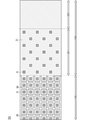
- the active region 100 includes a standard region portion 102 and a thinning region portion 101 between the standard region portion 102 and the outer peripheral region 200.
- the thinning area portion 101 is arranged adjacent to the standard area portion 102.
- the outer peripheral region 200 is arranged outside the standard region portion 102 via the thinning region portion 101.
- the thinned-out region portion 101 surrounds the standard region portion 102 that occupies most of the active region 100, and the thinned-out region portion 101 is surrounded by the outer peripheral region 200.
- the active region 100 is divided into a plurality of periodic region RPs.
- the active region 100 is formed by periodically and repeatedly arranging the periodic region RPs in a plurality of directions.
- each of the periodic region RPs has a square shape with a side length LP, and the active region 100 is formed by arranging a plurality of periodic region RPs along the sides. Is configured.
- the layout of the impurity region of each of the periodic region RPs will be described below.
- the unit cell UC0 is arranged in each of the periodic region RPs. Therefore, the standard region portion 102 is configured by periodically arranging the unit cells UC0.
- the unit cell U0 has a first well region 30, a source region 40, and a contact region 35.
- the unit cell U1 or the unit cell U2 is arranged in each of the plurality of periodic area RPs.
- the thinning area portion 101 includes at least one unit cell U1 and at least one unit cell U2.
- the pattern in which the unit cell U1 and the unit cell U2 coexist is preferably periodic.
- Unit cells U1 and unit cells U2 are arranged alternately.
- Each of the unit cell U1 and the unit cell U2 has a first well region 30 and a source region 40.
- the unit cell U1 has a contact region 35 like the unit cell U0.
- the unit cell U2 does not have a contact region 35.
- the outer edge pattern of the source region 40 of the unit cells U0 to U2 may be common.
- the first well region 30 of the unit cell U2 is directly connected to the first well region 30 of the unit cell U1 or indirectly via the first well region 30 of another unit cell U2.
- the first well region 30 of the unit cell U2 is directly connected to the first well region 30 of the unit cell U1.
- At least one of the first well regions 30 of the unit cell U1 and the unit cell U2 may have an extension that extends the shape of the first well region 30 of the unit cell U0 so that this connection is obtained.
- the first well region 30 of each of the unit cell U1 and the unit cell U2 has an expansion portion EX1 and an expansion portion EX2.
- Each of the extended portion EX1 and the extended portion EX2 is connected to the first well region 30 of the adjacent periodic region RP, and in particular, in the example shown in FIG. 2, the expanded portion EX1 and the extended portion EX2 are connected to each other. Has been done.
- the plurality of first well regions 30 have a polygonal shape repeatedly arranged in the in-plane direction, and in the example shown in FIG. 2, the plurality of first well regions 30 are repeatedly arranged along the x direction and the y direction. It has an arranged square shape. Further, if the expansion portion EX1 and the expansion portion EX2 are ignored, the plurality of first well regions 30 also have a polygonal shape repeatedly arranged in the in-plane direction even in the thinning region portion 101. In other words, if expansion EX1 and expansion EX2 are ignored, the plurality of first well regions 30 are repeatedly arranged in the in-plane direction in the entire active region 100 including the standard region 102 and the thinned region 101. It has a polygonal shape, and particularly in the example shown in FIG. 2, it has a square shape repeatedly arranged along the x-direction and the y-direction.
- the outer peripheral region 200 is provided with a second well region 31 that is larger than each first well region 30 of the standard region portion 102.
- a plurality of contact regions 35 are periodically arranged on the second well region 31.
- each first well region 30 of the standard region portion 102 has a square shape
- a rectangular shape having a long side and a short side may be used.
- Or other polygonal shapes may be used.
- FIG. 4 is a partial top view schematically showing the first well region 30, the second well region 31, and the surface region 71 in the field of view of FIG. 2, and the source region 40 (FIG. 2) is shown. do not have.
- the surface region 71 is defined as a region in which the portion of the upper surface of the SiC layer SL (FIG. 3) having a p-shape and the ohmic electrode 70 (FIG. 3) are in ohmic contact.
- the thinned-out area portion 101 has a lower surface density of the surface region 71 in a plan view than the standard region portion 102.
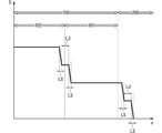
- FIG. 5 is a diagram showing the field of view in FIG. 4 enlarged in the vertical direction (y direction), and the definition of the above surface density will be described in detail with reference to this figure.
- the y direction is along the boundary line between the active region 100 and the outer peripheral region 200
- the x direction is a direction perpendicular to the boundary line.
- the rectangular region RR has a length LR in the x direction, a width WR in the y direction, and a center position CR.
- the value obtained by dividing the area of the surface area 71 in the rectangular area RR by the area of the rectangular area RR is defined as the area density in the position CR.
- the length LR is an integral multiple of the length LP (FIG.
- the width WR is an integral multiple of the length LP (FIG. 2), which is the period of the periodic region RP, specifically, is 10 times or more, and is the total width (dimension in the y direction) of the SiC layer SL. ) Is sufficiently smaller in length.
- the period of the periodic region RP is common in the x direction and the y direction has been described, but these may be different from each other.
- the thinned-out area portion 101 has a lower surface density of the surface region 71 in a plan view than the standard region portion 102.
- an example of a method for determining whether or not the surface density distribution satisfies this condition will be described.
- the areal density is calculated in a region sufficiently distant from the four corners of the chip.
- the center position CR (FIG. 5) is a position within a region sufficiently distant from the four corners of the chip.
- the length LR (FIG. 5) is 10 times the length LP (FIG. 2)
- the width WR (FIG. 5) is twice the length LP.
- FIG. 6 shows the relationship between the x-coordinate of the center position CR and the surface density S when the y-coordinate of the center position CR is constant.
- the surface density S in the thinning region portion 101 is lower than the surface density S in the standard region portion 102 (specifically, (It is about half), so the above conditions are met. Further, regardless of whether or not the vicinity of the boundary is ignored as described above, the average surface density S in the thinned area portion 101 is lower than the average surface density S in the standard region portion 102 (specifically). It is about half of the above), so the above conditions are met.
- a SiC substrate 10 having a 4H polytype, n-type, and low resistance silicon carbide is prepared.
- the plane orientation of the upper surface of the SiC substrate 10 has a slight off angle from the (0001) plane.
- a SiC layer SL having a thickness of 5 ⁇ m to 200 ⁇ m and having an n-type is formed by epitaxial growth by a chemical vapor deposition (CVD method).
- the n-type impurity concentration (donor concentration) is, for example, 1 ⁇ 10 14 cm -3 to 1 ⁇ 10 17 cm -3 .
- the SiC layer SL thus formed the portion other than the portion where the conductive type is inverted by ion implantation described later becomes the drift layer 20 for the MOSFET 711.
- an injection mask is formed on the upper surface of the SiC layer SL by a photoresist or the like.
- a p-type impurity (acceptor) Al (aluminum) is added to the upper surface of the SiC layer SL by ion implantation.
- the depth of this ion implantation does not exceed the thickness of the SiC layer SL, and is, for example, about 0.3 ⁇ m to 3 ⁇ m.
- the doping concentration of Al is higher than the impurity concentration of the drift layer 20, for example, in the range of 1 ⁇ 10 17 cm -3 to 1 ⁇ 10 19 cm -3 .
- the injection mask is removed.
- the regions to which the p-type is imparted by adding Al in this step become the first well region 30 and the second well region 31.
- some additional layer may be provided on the upper surface side of the SiC substrate 10 before forming the SiC layer SL, and in that case, this additional layer is regarded as a part of the SiC substrate 10.
- an n-type buffer layer having a higher concentration than that of the drift layer 20 may be formed.
- the n-type buffer layer can recombine a minority carrier that invades the SiC substrate 10 from the drift layer 20.
- a conversion layer that converts BPD existing on the surface of the SiC substrate 10 into through-blade dislocations may be formed by epitaxial growth in place of or in addition to the n-type buffer layer.
- an injection mask is formed on the upper surface of the SiC layer SL by a photoresist or the like.
- the p-type impurity Al is added to the upper surface of the SiC layer SL by ion implantation.
- the depth of this ion implantation does not exceed the thickness of the SiC layer SL, and is, for example, about 0.3 ⁇ m to 3 ⁇ m.
- the doping concentration of Al is higher than the impurity concentration of the drift layer 20 and lower than the impurity concentration of the second well region 31, for example, in the range of 1 ⁇ 10 16 cm -3 to 5 ⁇ 10 18 cm -3 . be. After that, the injection mask is removed. After that, the injection mask is removed.
- the region to which the p-type is imparted by adding Al in this step becomes the JTE region 37.
- the contact region 35 is formed by ion-implanting Al into a predetermined region on the surface of the first well region 30 at an impurity concentration higher than the impurity concentration of the first well region 30.
- an injection mask is formed by a photoresist or the like so that a predetermined portion inside the outer edge of the first well region 30 is exposed on the upper surface of the SiC layer SL.
- N nitrogen
- N of an n-type impurity (donor) is added to the upper surface of the SiC layer SL by ion implantation.
- the depth of this ion implantation is shallower than the thickness of the first well region 30.
- the doping concentration of N exceeds the p-type impurity concentration in the first well region 30, and is, for example, in the range of 1 ⁇ 10 18 cm -3 to 1 ⁇ 10 21 cm -3 .
- the region to which the n-type is added by adding N in this step becomes the source region 40.
- the heat treatment apparatus performs annealing in an atmosphere of an inert gas such as argon (Ar) gas at a temperature of 1300 ° C to 1900 ° C for 30 seconds to 1 hour.
- This annealing electrically activates N and Al added by ion implantation.
- a field insulating film 51 made of silicon oxide having a film thickness of 0.3 ⁇ m to 2 ⁇ m is formed on the SiC layer SL in a part of the outer peripheral region 200.
- the silicon oxide film as the gate insulating film 50 is formed by thermally oxidizing the portion of the upper surface of the SiC layer SL that is not covered with the field insulating film 51.
- a conductive polycrystalline silicon film is formed on the gate insulating film 50 and the field insulating film 51 by the reduced pressure CVD method.
- the gate electrode 60 is formed by patterning this polycrystalline silicon film.
- the interlayer insulating film 55 made of silicon oxide is formed by the reduced pressure CVD method. Subsequently, a contact hole 90 is formed that penetrates the interlayer insulating film 55 and the gate insulating film 50 and reaches the contact region 35 and the source region 40 in the active region 100. Similarly, a contact hole 91 that reaches the second well region 31 is formed.
- a metal film containing Ni as a main component is formed by a sputtering method or the like. Then, by heat treatment at a temperature of 600 ° C. to 1100 ° C., the Ni atom of the metal film and the Si atom of the SiC layer SL are reacted in the contact hole 90 and the contact hole 91 to cause the SiC layer SL and the metal.
- a silicide layer as an ohmic electrode 70 is formed between the film and the film. Subsequently, the portion of the metal film that has not changed to the silicide layer is removed by wet etching.
- a metal film containing Ni as a main component is formed on the back surface of the SiC substrate 10.
- a back surface ohmic electrode (not shown) is formed.
- the contact hole 95 penetrating the interlayer insulating film 55 is formed by etching using a photoresist or the like as a mask.
- a part of the source electrode 80 is formed on the ohmic electrode 70 in the contact hole 90 and the contact hole 91 by the film formation by the sputtering method or the like and the patterning by the photolithography method or the like.
- the balance of the source electrode 80, the gate pad 81, and the gate wiring 82 are formed by depositing a wiring metal such as Al by a sputtering method or a vapor deposition method and patterning by a photolithography method or the like. It is formed.
- the drain electrode 84 is formed on the surface of the back surface ohmic electrode (not shown) formed on the back surface of the SiC substrate 10. With the above, the MOSFET 711 is completed.
- the state of the channel region of the MOSFET 711 is switched between an on state and an off state.
- the off state there is a period in which the drain voltage (voltage of the drain electrode 84) becomes lower than the source voltage (voltage of the source electrode 80), and at this time, the drain voltage becomes, for example, ⁇ several V to ⁇ 10) V.
- the MOSFET 711 performs a reflux operation.
- the pn junction formed by the first well region 30 and the second well region 31 ohmicly connected to the source electrode 80 and the drift layer 20 ohmicly connected to the drain electrode 84.
- a forward voltage of more than 2 V, which corresponds to the diffusion potential, is applied. That is, a voltage exceeding the forward voltage is applied to the body diode of the MOSFET 711.
- the MOSFET 711 operates as a freewheeling diode. Therefore, a large bipolar current flows in the direction from the source electrode 80 to the drain electrode 84. When the current density of this current is 100 A / cm 2 or more, significant conductivity modulation occurs in the drift layer 20.
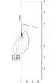
- FIG. 7 is a cross-sectional view modeling a body diode of a comparative example in which the surface density S (FIG. 6) is substantially uniform in the active region 100 (FIG. 3).
- the cathode electrode 84D, the SiC substrate 10D, the SiC layer SLD, and the anode electrode 80D are set by modeling each of the drain electrode 84, the SiC substrate 10, the SiC layer SL, and the source electrode 80 in the MOSFET 711 (FIG. 3).
- the SiC layer SLD has a drift layer 20D that models the drift layer 20 (FIG. 3) and a well region 30D that models the first well region 30 and the second well region 31 (FIG. 3).
- the SiC substrate 10 has a thickness t sub , the drift layer 20D has a thickness t drift , and the sum of these has a thickness t tot .
- the left end of the model of FIG. 7 corresponds to the center position of the active region 100 (FIG. 3).
- the electrode width LA is the dimension from the center position to the outer edge of the anode electrode 80D
- the electrode width LC is the dimension from the center position to the outer edge of the cathode electrode 84D.
- the vertical dimensions are exaggerated to make the drawing easier to see, and in the actual dimensions, the electrode width LA and the electrode width LC are much larger than the thickness t tot . ..
- FIG. 8 shows the simulation results of the current density when a current corresponding to 1000 A per unit area of the anode electrode 80D is applied to the center position (left end position in FIG. 7) of the anode electrode 80D (FIG. 7). It is a distribution map which shows in the vicinity of the end of the electrode 80D. According to this simulation, the region where the current density becomes extremely high appears in an elliptical shape centered on the end portion of the anode electrode 80D.
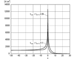
- the thickness tsub of the SiC substrate 10 is large, the peak value and the peak width of the current density are larger, which indicates that the thickness tsub of the SiC substrate 10 affects the state of current concentration.
- the current spread in the drift layer 20D and the current spread in the SiC substrate 10D are almost continuous. It is considered that this is because the resistivity of the drift layer 20D is reduced to about the resistivity of the SiC substrate 10D due to the conductivity modulation.
- the thickness t tot of the resistor that includes both the SiC substrate 10D and the drift layer 20D is relative to the current density distribution. It is considered to have a more direct correlation.
- the current density is 10% based on the current density on the center side of the anode electrode 80D (current density on the left end side in the graph of FIG. 9) in any of the two thickness conditions.
- the position where the current density is 30% higher than the current density on the center side of the anode electrode 80D is a position at a distance of 30% of the thickness t tot inward from the end position of the anode electrode 80D.
- the position where the current density is 50% higher than the current density on the center side of the anode electrode 80D is a position 20% of the thickness t tot inward from the end position of the anode electrode 80D.
- the width (dimension in the x direction) of the thinned-out region portion 101 is 20% or more of the sum of the thickness of the SiC substrate 10 (FIG. 3) and the thickness of the SiC layer SL (FIG. 3). It is preferably 30% or more, more preferably 50% or more, and even more preferably 50% or more.
- FIG. 10 is a graph showing the simulation results of the hole concentration distribution under the same conditions as in FIG. As for the hole concentration distribution, the same distribution as the current density distribution (Fig. 9) can be seen. Therefore, it is considered that the local increase in the hole concentration can be suppressed by adopting the configuration that relaxes the concentration of the current density. It is considered that a highly reliable silicon carbide semiconductor device can be realized by suppressing the deterioration of the characteristics of the body diode.
- the width of the thinned-out region portion 101 is set so as to suppress this new increase, it is presumed that the above-mentioned effect can be obtained more reliably. Analyzing the simulation results of FIG. 10, the position where the hole concentration is 1% higher than the hole concentration on the center side of the anode electrode 80D (the hole concentration on the left end side in the graph of FIG. 10) is the end of the anode electrode 80D.
- the width (dimension in the x direction) of the thinned out region portion 101 is 110% or less of the sum of the thickness of the SiC substrate 10 (FIG. 3) and the thickness of the SiC layer SL (FIG. 3). It is preferably 70% or more, and more preferably 70% or more.
- FIG. 11 is a cross-sectional view modeling the body diode in consideration of the difference in the surface density S (FIG. 6) in the active region 100 (FIG. 3).
- the difference from the model of FIG. 7 described above is that the contact resistivity is defined at the boundary between the anode electrode 80D and the well region 30D in order to model the difference in the surface density S in the active region.
- the contact resistivity ⁇ ct ⁇ cc ⁇ TM ( ⁇ ⁇ cm 2 ) (TM is a coefficient) in the range corresponding to (FIG. 3).
- FIG. 12 shows the simulation results of the hole concentration distribution when a current corresponding to 1000 A per unit area of the anode electrode 80D is applied to the center position (left end position in FIG. 11) of the anode electrode 80D (FIG. 11).
- the average contact resistivity in the thinned area portion 101 is 1.5 times or more the average contact resistivity in the standard region portion 102. .. Since the contact resistivity of the surface region 71 is considered to be almost constant, it is necessary to change the surface density of the surface region 71 in order to change the distribution of the average contact resistivity. It is preferable that the surface density of the surface region 71 of the thinning region portion 101 is 2/3 or less of the surface density of the surface region 71 of the standard region portion 102 in order to obtain the distribution of.
- the surface density of the surface area 71 of the thinned area portion 101 is preferably 1/10 or more of the surface density of the surface area 71 of the standard region portion 102.
- the thinned-out area portion 101 has a lower surface density S (FIG. 6) of the surface region 71 (FIG. 4) in a plan view than the standard region portion 102. Since such a surface density distribution can be obtained without particularly complicating the manufacturing method, it does not lead to a significant increase in manufacturing cost. Since the surface density S of the surface region 71 of the thinned region portion 101 is lower than that of the standard region portion 102, the bipolar current is locally increased in the local region near the boundary between the outer peripheral region 200 and the active region 100. Is suppressed. As a result, the expansion of stacking defects can be sufficiently suppressed even in the local region.
- the contact resistivity of the thinned region portion 101 is 1. It is 5 times or more and 10 times or less.
- the width (horizontal dimension in FIG. 2) of the thinned-out region portion 101 is 20% or more of the sum of the thickness of the SiC substrate 10 (FIG. 3) and the thickness of the SiC layer SL (FIG. 3), it is shown in FIG.
- the local increase in the bipolar current is suppressed in approximately the entire range in which the local increase in the bipolar current is particularly large. It should be noted that this effect is more sufficiently obtained when the percentage reaches about 70%, and is approximately ideally obtained when the percentage reaches about 110% for the reason described above in relation to the simulation. Therefore, from the viewpoint of avoiding an excessive proportion of the thinned-out region portion 101 in the active region 100, the upper limit of the percentage may be 110%, and further may be 70%.
- the current density of the MOSFET 711 in the ON state may be 100 A / cm 2 or more, and when the current density is such a large value, a large amount of holes flow into the drift layer 20 to cause significant conductivity modulation. Therefore, the resistivity of the drift layer 20 is significantly reduced. According to the present embodiment, the local increase in the bipolar current generated under such conditions can be effectively suppressed.
- the plurality of first well regions 30 (FIG. 4) in the standard region portion 102 have a polygonal shape (specifically, a rectangular shape, more specifically, a square shape) in which the first well regions 30 (FIG. 4) are repeatedly arranged. is doing. Thereby, a polygonal outer edge can be provided in each of the plurality of first well regions 30 in a plan view.
- FIG. 13 is a partial top view showing a MOSFET 712 (silicon carbide semiconductor device) as a first modification of the MOSFET 711 (FIG. 4).
- MOSFET 712 silicon carbide semiconductor device
- the surface region 71 is arranged outside the second well region 31.
- the ohmic electrode 70 (FIG. 3) is arranged off the second well region 31.
- the second well region 31 (FIG. 13) is connected to the first well region 30 at the boundary between the outer peripheral region 200 and the active region 100.
- FIG. 14 is a partial top view showing a MOSFET 713 (silicon carbide semiconductor device) as a second modification of the MOSFET 711 (FIG. 4). Unlike the MOSFET 711 (FIG. 4), in the MOSFET 713 (FIG. 14), the plurality of first well regions 30 have a striped shape in the in-plane direction.
- MOSFET 713 silicon carbide semiconductor device
- FIG. 15 is a partial top view showing a MOSFET 714 (silicon carbide semiconductor device) as a third modification of the MOSFET 711 (FIG. 4).
- the surface region 71 is arranged outside the second well region 31 as in the MOSFET 712 (FIG. 13), and a plurality of positions in the in-plane direction are arranged as in the MOSFET 713 (FIG. 14).
- the 1-well region 30 has a striped shape.
- FIG. 16 is a partial top view showing a MOSFET 715 (silicon carbide semiconductor device) as a fourth modification of the MOSFET 711 (FIG. 4).
- MOSFET 715 silicon carbide semiconductor device
- FIG. 14 With respect to the surface area 71, the area density of the thinned area portion 101 decreases toward the outside (right side in FIG. 16).
- the thinning area portion 101 is composed of a plurality of portions from the inside to the outside (toward the right side in FIG. 16), and the surface density of these plurality of portions decreases toward the outside. .. Therefore, the surface density of the thinned-out area portion 101 has a plurality of levels.
- the thinned-out region portion 101 is composed of the portion 101a and the portion 101b from the inside to the outside, and the surface density of the portion 101b is lower than the surface density of the portion 101a. Therefore, the surface density of the thinned-out region portion 101 has a relatively high level in the portion 101a and a relatively low level in the portion 101b.
- the degree of freedom in designing the distribution of the surface density is improved, and therefore, the width (horizontal dimension in FIG. 16) of the thinned-out area portion 101 is further suppressed, and the above-described first embodiment is performed.
- the number of surface density levels is two is illustrated in FIG. 16, the number of surface density levels is not limited to two, and as a modification, the number of levels is sufficiently large. By doing so, a configuration may be used in which the surface density of the thinned-out area portion 101 decreases substantially continuously toward the outside.
- the second well region 31 may be located depending on the position and direction of the diagonal straight line. It appears separated from the first well region 30 (similar to the case of FIG. 3). Therefore, in common with the first embodiment and its modifications, the first well region 30 and the second well region 31 are separated from each other in at least one cross-sectional view.
- FIG. 17 is a partial top view schematically showing the configuration of the MOSFET 721 according to the second embodiment in the same field of view as the field of view of FIG. 4 (first embodiment).
- the active region 100 does not need to have the thinned out region portion 101 (FIG. 4), for example, only from the standard region portion 102 (FIG. 4). It may be configured.
- the outer peripheral region 200 includes an outer region portion 202 and a thinning region portion 201 between the outer region portion 202 and the active region 100.
- the thinned area portion 201 has a lower surface density of the surface region 71 in a plan view than the active region 100. Further, the preferable relationship between the surface density of the standard region portion 102 (FIG. 4) and the surface density of the thinned region portion 101 (FIG. 4) described in the first embodiment is the active region 100 in the second embodiment. It may also be applied to the relationship between (FIG. 17) and the thinned area portion 201 (FIG. 17).
- Embodiment 3 In this embodiment, any one of the above-described embodiments or any of the silicon carbide semiconductor devices (PWMs 711 to 715 and 721) according to the modified example thereof is applied to the power conversion device.
- the application of these silicon carbide semiconductor devices is not limited to a specific power conversion device, but the case where these silicon carbide semiconductor devices are applied to a three-phase inverter will be described below as the third embodiment.
- FIG. 18 is a block diagram showing the configuration of the power conversion system according to the third embodiment.
- the power conversion system includes a power supply 910, a power conversion device 920, and a load 930.
- the power supply 910 is a DC power supply and supplies DC power to the power conversion device 920.
- the power supply 910 may be composed of, for example, a DC system, a solar cell, or a storage battery, or may be composed of a rectifier circuit or an AC / DC converter connected to an AC system.
- the power supply 910 may be configured by a DC / DC converter that converts the DC power output from the DC system into a predetermined power.
- the power conversion device 920 is a three-phase inverter connected between the power supply 910 and the load 930, converts the DC power supplied from the power supply 910 into AC power, and supplies AC power to the load 930.
- the power conversion device 920 controls a main conversion circuit 921 that converts DC power into AC power and outputs it, a drive circuit 922 that outputs a drive signal that drives each switching element of the main conversion circuit 921, and a drive circuit 922. It has a control circuit 923 that outputs a control signal to the drive circuit 922.
- the load 930 is a three-phase electric motor driven by AC power supplied from the power conversion device 920.
- the load 930 is not limited to a specific application, and is, for example, an electric motor mounted on various electric devices, and is used as an electric motor for, for example, a hybrid vehicle, an electric vehicle, a railroad vehicle, an elevator, or an air conditioner. Will be.
- the details of the power conversion device 920 will be described below.
- the main conversion circuit 921 receives the input power from the power supply 910, converts the input power into the output power, and outputs the output power to the load 930.
- the main conversion circuit 921 has a switching element and a freewheeling diode (not shown), and the switching element switches to convert the DC power supplied from the power supply 910 into AC power. Supply to load 930.
- the main conversion circuit 921 according to the third embodiment is a two-level three-phase full bridge circuit, and has six switching elements and their respective switching elements. It can be composed of six freewheeling diodes connected in antiparallel to.
- each switching element of the main conversion circuit 921 a silicon carbide semiconductor device according to any one of the above-described embodiments or a modification thereof is applied.
- the six switching elements are connected in series for each of the two switching elements, thereby forming three upper and lower arms.
- Each upper and lower arm constitutes each phase (U phase, V phase, W phase) of the full bridge circuit.
- the output terminals of each upper and lower arm that is, the three output terminals of the main conversion circuit 921 are connected to the load 930.
- the drive circuit 922 generates a drive signal for driving the switching element of the main conversion circuit 921, and supplies the drive signal to the control electrode of the switching element of the main conversion circuit 921. Specifically, the drive circuit 922 uses a drive signal for turning on the switching element and a drive signal for turning off the switching element in the control electrode of each switching element according to the control signal from the control circuit 923 described later. Output.
- the drive signal is a voltage signal (on signal) equal to or higher than the threshold voltage of the switching element, and when the switching element is kept off, the drive signal is a voltage lower than the threshold voltage of the switching element. It is a signal (off signal).
- the control circuit 923 controls the switching element of the main conversion circuit 921 via the drive circuit 922 so that the desired power is supplied to the load 930.
- the control circuit 923 calculates the time (on time) for each switching element of the main conversion circuit 921 to be in the on state based on the electric power to be supplied to the load 930.
- the main conversion circuit 921 can be controlled by PWM control that modulates the on-time of the switching element according to the voltage to be output.
- the control circuit 923 outputs a control signal (control command) for controlling the drive circuit 922 to the drive circuit 922.
- the drive circuit 922 outputs an on signal or an off signal as a drive signal to the control electrode of each switching element.
- the control signal of the control circuit 923 is generated from the drive circuit 922 at each time point so that the on signal is output to the switching element that should be turned on and the off signal is output to the switching element that should be turned off. ..
- the silicon carbide semiconductor device according to any one of the above-described embodiments or a modification thereof is applied as the switching element of the main conversion circuit 921, the manufacturing cost is significantly increased. While avoiding it, it is possible to realize a power conversion device in which deterioration of characteristics is suppressed.
- a two-level three-phase inverter is exemplified as the power conversion device, but the power conversion device to which the silicon carbide semiconductor device according to any one of the above-described embodiments or a modification thereof is applied is to this. Not limited.
- the power conversion device may be, for example, a multi-level power conversion device having three or more levels, or a single-phase inverter that supplies power to a single-phase load.
- the power conversion device may be a DC / DC converter or an AC / DC converter.
- the power conversion device to which the silicon carbide semiconductor device according to any one of the above-described embodiments or a modification thereof is applied may be used not only when the above-mentioned load is an electric motor.
- the power converter may be used as a power supply for an electric discharge machine, a laser machine, an induction cooker, or a contactless power supply system.
- the power conversion device may be used as a power conditioner for a photovoltaic power generation system, a power storage system, or the like.
- SiC substrate Si carbide substrate
- 20 drift layer 30 1st well region, 31 2nd well region, 35 contact region, 40 source region, 50 gate insulating film, 60 gate electrode, 70 ohmic electrode, 71 plane region, 80 source electrode, 81 gate pad, 82 gate wiring, 84 drain electrode, 100 active region, 101, 201 thinning region, 102 standard region, 200 outer peripheral region, 202 outer region, 711 to 715,721 MOSFET (silicon carbide) Semiconductor device), 910 power supply, 920 power conversion device, 921 main conversion circuit, 922 drive circuit, 923 control circuit, 930 load, SL SiC layer (silicon carbide layer).
Landscapes
- Electrodes Of Semiconductors (AREA)
Abstract
Description
<1-1. 基本的構成>
図1は、本実施の形態1に係るMOSFET711(炭化珪素半導体装置)の構成を概略的に示す上面図である。MOSFET711はその上面に、ソース電極80と、ゲートパッド81と、ゲート配線82とを有している。ゲート配線82はゲートパッド81から延びており、これらから離れてソース電極80が配置されている。
図2を参照して、活性領域100は、標準領域部102と、標準領域部102と外周領域200との間の間引き領域部101と、を含む。間引き領域部101は、標準領域部102に隣接して配置されている。標準領域部102の外側に間引き領域部101を介して外周領域200が配置されている。典型的には、活性領域100の大部分の割合を占める標準領域部102を間引き領域部101が取り囲み、この間引き領域部101を外周領域200が取り囲む。
次に、MOSFET711の製造方法の例について、以下に説明する。
次に、MOSFET711の動作、特にその還流動作、について、SiC層SLのSiC材料がポリタイプ4Hを有する場合を例にして、以下に説明する。なおポリタイプ4HのSiCのpn接合の拡散電位は、おおよそ2Vである。
上記還流動作において、面密度S(図6)の分布が最適化されていないと活性領域100と外周領域200との境界近傍などにおいて電流密度が局所的に増大し、一方、本実施の形態のように面密度S(図6)の分布が最適化されていると当該増大を抑制することができる。このことについて説明するため、縦型MOSFETに含まれるボディダイオードをモデル化しての2次元T-CADシミュレーションについて、以下に記す。
本実施の形態によれば、間引き領域部101は標準領域部102に比して平面視における面領域71(図4)の面密度S(図6)が低い。このような面密度の分布は、製造方法を特段に複雑化することなく得られるので、製造コストの顕著な増大にはつながらない。そして、間引き領域部101が標準領域部102に比して面領域71の面密度Sが低いことによって、外周領域200と活性領域100との境界近傍の局所的領域におけるバイポーラ電流の局所的な増大が抑制される。これにより、当該局所的領域においても積層欠陥の拡張を十分に抑制することができる。よって、SiC層SL(図3)における積層欠陥の拡張に起因してのMOSFET711の特性劣化を十分に抑制することができる。以上から、製造コストの顕著な増大を避けつつMOSFET711の特性劣化を抑制することができる。
図13は、MOSFET711(図4)の第1変形例としてのMOSFET712(炭化珪素半導体装置)を示す部分上面図である。MOSFET711(図4)と異なりMOSFET712(図13)においては、面領域71が第2ウェル領域31から外れて配置されている。言い換えれば、オーミック電極70(図3)が第2ウェル領域31上から外れて配置されている。また上記実施の形態1と異なり本変形例においては、第2ウェル領域31(図13)は、外周領域200と活性領域100との境界部において第1ウェル領域30に接続されている。
図17は、本実施の形態2に係るMOSFET721の構成を、図4(実施の形態1)の視野と同様の視野で概略的に示す部分上面図である。
本実施の形態は、前述した実施の形態のいずれかまたはその変形例に係る炭化珪素半導体装置(MOSFET711~715および721)のいずれかを電力変換装置に適用したものである。これら炭化珪素半導体装置の適用は特定の電力変換装置に限定されるものではないが、以下、実施の形態3として、三相のインバータに、これら炭化珪素半導体装置を適用した場合について説明する。
Claims (11)
- 炭化珪素半導体装置であって、
第1導電型を有する炭化珪素基板と、
前記炭化珪素基板に面する第1面と、厚み方向において前記第1面と反対の第2面とを有し、前記厚み方向に垂直な面内方向において活性領域と前記活性領域の外周に配置された外周領域とを有する炭化珪素層と、を備え、前記炭化珪素層は、
前記炭化珪素基板上に配置され、前記第1導電型を有するドリフト層と、
前記活性領域において前記ドリフト層上に配置され、前記第1導電型と異なる第2導電型を有し、少なくとも一の断面視において互いに分離されている複数の第1ウェル領域と、
前記複数の第1ウェル領域上に配置され、前記第1導電型を有する複数のソース領域と、
前記外周領域において前記ドリフト層上に配置され、前記第2導電型を有する第2ウェル領域と、を含み、前記炭化珪素半導体装置はさらに、
前記複数の第1ウェル領域に面するゲート絶縁膜と、
前記活性領域の上方に配置され前記ゲート絶縁膜を介して前記複数の第1ウェル領域に面する部分と、前記外周領域の上方に配置され前記第2ウェル領域から絶縁された部分と、を有するゲート電極と、
前記第2ウェル領域の上方に配置され、前記第2ウェル領域から絶縁され、前記ゲート電極に接続されたゲートパッドと、
前記炭化珪素層の前記第2面の上方に設けられたソース電極と、
前記炭化珪素層の前記第2面上に設けられ、前記ソース電極に接続され、前記複数の第1ウェル領域に電気的にオーミックに接続され、前記炭化珪素層の前記第2面のうち前記第2導電型を有する部分にオーミックに接触する複数の面領域を有する複数のオーミック電極と、を備え、
前記活性領域は、標準領域部と、前記標準領域部と前記外周領域との間の間引き領域部と、を含み、前記間引き領域部は前記標準領域部に比して平面視における前記複数の面領域の面密度が低いことを特徴とする炭化珪素半導体装置。 - 前記複数のオーミック電極が前記第2ウェル上から外れて配置されていることを特徴とする請求項1に記載の炭化珪素半導体装置。
- 前記面内方向において前記複数の第1ウェル領域がストライプ形状を有していることを特徴とする請求項1または2に記載の炭化珪素半導体装置。
- 前記面内方向において前記複数の第1ウェル領域が、前記標準領域部において、繰り返し配列された多角形形状を有していることを特徴とする請求項1または2に記載の炭化珪素半導体装置。
- 炭化珪素半導体装置であって、
第1導電型を有する炭化珪素基板と、
前記炭化珪素基板に面する第1面と、厚み方向において前記第1面と反対の第2面とを有し、前記厚み方向に垂直な面内方向において活性領域と前記活性領域の外周に配置された外周領域とを有する炭化珪素層と、を備え、前記炭化珪素層は、
前記炭化珪素基板上に配置され、前記第1導電型を有するドリフト層と、
前記活性領域において前記ドリフト層上に配置され、前記第1導電型と異なる第2導電型を有し、少なくとも一の断面視において互いに分離されている複数の第1ウェル領域と、
前記複数の第1ウェル領域上に配置され、前記第1導電型を有する複数のソース領域と、
前記外周領域において前記ドリフト層上に配置され、前記第2導電型を有する第2ウェル領域と、を含み、前記炭化珪素半導体装置はさらに、
前記複数の第1ウェル領域に面するゲート絶縁膜と、
前記活性領域の上方に配置され前記ゲート絶縁膜を介して前記複数の第1ウェル領域に面する部分と、前記外周領域の上方に配置され前記第2ウェル領域から絶縁された部分と、を有するゲート電極と、
前記第2ウェル領域の上方に配置され、前記第2ウェル領域から絶縁され、前記ゲート電極に接続されたゲートパッドと、
前記炭化珪素層の前記第2面の上方に設けられたソース電極と、
前記炭化珪素層の前記第2面上に設けられ、前記ソース電極に接続され、前記複数の第1ウェル領域および前記第2ウェル領域に電気的にオーミックに接続され、前記炭化珪素層の前記第2面のうち前記第2導電型を有する部分にオーミックに接触する複数の面領域を有する複数のオーミック電極と、を備え、
前記外周領域は、外側領域部と、前記外側領域部と前記活性領域との間の間引き領域部と、を含み、前記間引き領域部は前記活性領域に比して平面視における前記複数の面領域の面密度が低いことを特徴とする炭化珪素半導体装置。 - 前記間引き領域部の幅が、前記炭化珪素基板の厚みと前記炭化珪素層の厚みとの和の20%以上であることを特徴とする請求項1から5のいずれか1項に記載の炭化珪素半導体装置。
- 前記間引き領域部の前記面密度が前記活性領域の前記面密度の1/10以上2/3以下であることを特徴とする請求項1から6のいずれか1項に記載の炭化珪素半導体装置。
- 前記間引き領域部の面密度が外側に向かうにつれて低下することを特徴とする請求項1から7のいずれか1項に記載の炭化珪素半導体装置。
- 前記間引き領域部の面密度が複数の水準を有していることを特徴とする請求項1から8のいずれか1項に記載の炭化珪素半導体装置。
- オン状態における電流密度が100A/cm2以上である請求項1から9のいずれか1項に記載の炭化珪素半導体装置。
- 請求項1から10のいずれか1項に記載の炭化珪素半導体装置を有し、入力電力を受け付け、前記入力電力を出力電力へ変換し、前記出力電力を出力する主変換回路と、
前記炭化珪素半導体装置を駆動する駆動信号を前記炭化珪素半導体装置に出力する駆動回路と、
前記駆動回路を制御する制御信号を前記駆動回路に出力する制御回路と、
を備えた電力変換装置。
Priority Applications (5)
| Application Number | Priority Date | Filing Date | Title |
|---|---|---|---|
| US18/008,448 US12520550B2 (en) | 2020-08-11 | 2020-08-11 | Silicon carbide semiconductor device and power converter |
| DE112020007503.6T DE112020007503T5 (de) | 2020-08-11 | 2020-08-11 | Siliciumcarbid-halbleitereinheit und leistungswandler |
| PCT/JP2020/030578 WO2022034636A1 (ja) | 2020-08-11 | 2020-08-11 | 炭化珪素半導体装置および電力変換装置 |
| CN202080104747.5A CN116137935B (zh) | 2020-08-11 | 2020-08-11 | 碳化硅半导体装置以及电力变换装置 |
| JP2022542523A JP7332812B2 (ja) | 2020-08-11 | 2020-08-11 | 炭化珪素半導体装置および電力変換装置 |
Applications Claiming Priority (1)
| Application Number | Priority Date | Filing Date | Title |
|---|---|---|---|
| PCT/JP2020/030578 WO2022034636A1 (ja) | 2020-08-11 | 2020-08-11 | 炭化珪素半導体装置および電力変換装置 |
Publications (1)
| Publication Number | Publication Date |
|---|---|
| WO2022034636A1 true WO2022034636A1 (ja) | 2022-02-17 |
Family
ID=80247785
Family Applications (1)
| Application Number | Title | Priority Date | Filing Date |
|---|---|---|---|
| PCT/JP2020/030578 Ceased WO2022034636A1 (ja) | 2020-08-11 | 2020-08-11 | 炭化珪素半導体装置および電力変換装置 |
Country Status (5)
| Country | Link |
|---|---|
| US (1) | US12520550B2 (ja) |
| JP (1) | JP7332812B2 (ja) |
| CN (1) | CN116137935B (ja) |
| DE (1) | DE112020007503T5 (ja) |
| WO (1) | WO2022034636A1 (ja) |
Citations (4)
| Publication number | Priority date | Publication date | Assignee | Title |
|---|---|---|---|---|
| JP2015115452A (ja) * | 2013-12-11 | 2015-06-22 | 三菱電機株式会社 | 半導体装置 |
| WO2015166754A1 (ja) * | 2014-05-01 | 2015-11-05 | 三菱電機株式会社 | 半導体装置 |
| WO2017169086A1 (ja) * | 2016-03-30 | 2017-10-05 | 三菱電機株式会社 | 半導体装置およびその製造方法、電力変換装置 |
| JP2018046162A (ja) * | 2016-09-14 | 2018-03-22 | 富士電機株式会社 | 炭化珪素半導体装置 |
Family Cites Families (7)
| Publication number | Priority date | Publication date | Assignee | Title |
|---|---|---|---|---|
| JP2011100877A (ja) * | 2009-11-06 | 2011-05-19 | Toshiba Corp | 半導体装置及びその製造方法 |
| JP5719167B2 (ja) * | 2010-12-28 | 2015-05-13 | ルネサスエレクトロニクス株式会社 | 半導体装置 |
| DE112014006733B4 (de) | 2014-06-11 | 2021-10-07 | Hitachi, Ltd. | Halbleitervorrichtung, Leistungsmodul, Leistungsumsetzer und Halbleitervorrichtungs-Herstellungsverfahren |
| JP6611960B2 (ja) * | 2016-11-01 | 2019-11-27 | 三菱電機株式会社 | 炭化珪素半導体装置および電力変換装置 |
| CN206490069U (zh) * | 2017-01-24 | 2017-09-12 | 深圳基本半导体有限公司 | 一种宽禁带半导体器件 |
| WO2018155553A1 (ja) | 2017-02-24 | 2018-08-30 | 三菱電機株式会社 | 炭化珪素半導体装置および電力変換装置 |
| JP6874158B2 (ja) * | 2017-12-19 | 2021-05-19 | 三菱電機株式会社 | 炭化珪素半導体装置および電力変換装置 |
-
2020
- 2020-08-11 WO PCT/JP2020/030578 patent/WO2022034636A1/ja not_active Ceased
- 2020-08-11 US US18/008,448 patent/US12520550B2/en active Active
- 2020-08-11 JP JP2022542523A patent/JP7332812B2/ja active Active
- 2020-08-11 CN CN202080104747.5A patent/CN116137935B/zh active Active
- 2020-08-11 DE DE112020007503.6T patent/DE112020007503T5/de active Pending
Patent Citations (4)
| Publication number | Priority date | Publication date | Assignee | Title |
|---|---|---|---|---|
| JP2015115452A (ja) * | 2013-12-11 | 2015-06-22 | 三菱電機株式会社 | 半導体装置 |
| WO2015166754A1 (ja) * | 2014-05-01 | 2015-11-05 | 三菱電機株式会社 | 半導体装置 |
| WO2017169086A1 (ja) * | 2016-03-30 | 2017-10-05 | 三菱電機株式会社 | 半導体装置およびその製造方法、電力変換装置 |
| JP2018046162A (ja) * | 2016-09-14 | 2018-03-22 | 富士電機株式会社 | 炭化珪素半導体装置 |
Also Published As
| Publication number | Publication date |
|---|---|
| JP7332812B2 (ja) | 2023-08-23 |
| JPWO2022034636A1 (ja) | 2022-02-17 |
| CN116137935A (zh) | 2023-05-19 |
| US12520550B2 (en) | 2026-01-06 |
| CN116137935B (zh) | 2024-11-01 |
| DE112020007503T5 (de) | 2023-06-07 |
| US20230215921A1 (en) | 2023-07-06 |
Similar Documents
| Publication | Publication Date | Title |
|---|---|---|
| US11637184B2 (en) | Silicon carbide semiconductor device, power converter, method of manufacturing silicon carbide semiconductor device, and method of manufacturing power converter | |
| US11158704B2 (en) | Semiconductor device and power conversion device | |
| JP2019195081A (ja) | 半導体装置および電力変換装置 | |
| JP6962511B1 (ja) | 半導体装置、及び電力変換装置 | |
| JPWO2018155566A1 (ja) | 炭化珪素半導体装置および電力変換装置 | |
| JP2021108396A (ja) | 炭化珪素半導体装置および電力変換装置 | |
| JPWO2021014570A1 (ja) | 炭化珪素半導体装置、電力変換装置および炭化珪素半導体装置の製造方法 | |
| JP7370476B2 (ja) | 炭化珪素半導体装置の製造方法、炭化珪素半導体装置および電力変換装置 | |
| JP7004117B1 (ja) | 炭化珪素半導体装置および電力変換装置 | |
| JP7047981B1 (ja) | 炭化珪素半導体装置および電力変換装置 | |
| JP2019096631A (ja) | 半導体装置および電力変換装置 | |
| US12568638B2 (en) | Semiconductor device and power conversion apparatus | |
| JPWO2020188686A1 (ja) | 炭化珪素半導体装置および電力変換装置 | |
| JP6873273B2 (ja) | 炭化珪素半導体装置および電力変換装置 | |
| JP7330396B2 (ja) | 半導体装置及び電力変換装置 | |
| JPWO2021044624A1 (ja) | 炭化珪素半導体装置および電力変換装置 | |
| JP7275407B1 (ja) | 炭化珪素半導体装置、電力変換装置および炭化珪素半導体装置の製造方法 | |
| JP7062143B1 (ja) | 半導体装置及び電力変換装置 | |
| US20240355922A1 (en) | Semiconductor device, power conversion apparatus, and method of manufacturing semiconductor device | |
| JP7332812B2 (ja) | 炭化珪素半導体装置および電力変換装置 | |
| JP7529139B2 (ja) | 炭化珪素半導体装置とその製造方法、および、電力変換装置 | |
| US12471328B2 (en) | Semiconductor device, electric power conversion device, and method for manufacturing semiconductor device | |
| WO2024038504A1 (ja) | 炭化珪素半導体装置、電力変換装置および炭化珪素半導体装置の製造方法 | |
| JP2023008566A (ja) | 半導体装置及び電力変換装置 |
Legal Events
| Date | Code | Title | Description |
|---|---|---|---|
| 121 | Ep: the epo has been informed by wipo that ep was designated in this application |
Ref document number: 20949498 Country of ref document: EP Kind code of ref document: A1 |
|
| ENP | Entry into the national phase |
Ref document number: 2022542523 Country of ref document: JP Kind code of ref document: A |
|
| NENP | Non-entry into the national phase |
Ref country code: DE |
|
| 122 | Ep: pct application non-entry in european phase |
Ref document number: 20949498 Country of ref document: EP Kind code of ref document: A1 |
|
| WWG | Wipo information: grant in national office |
Ref document number: 18008448 Country of ref document: US |