WO2022018816A1 - Module optique - Google Patents
Module optique Download PDFInfo
- Publication number
- WO2022018816A1 WO2022018816A1 PCT/JP2020/028177 JP2020028177W WO2022018816A1 WO 2022018816 A1 WO2022018816 A1 WO 2022018816A1 JP 2020028177 W JP2020028177 W JP 2020028177W WO 2022018816 A1 WO2022018816 A1 WO 2022018816A1
- Authority
- WO
- WIPO (PCT)
- Prior art keywords
- waveguide
- optical
- optical module
- fiber
- plc
- Prior art date
Links
Images


Classifications
-
- G—PHYSICS
- G02—OPTICS
- G02B—OPTICAL ELEMENTS, SYSTEMS OR APPARATUS
- G02B6/00—Light guides; Structural details of arrangements comprising light guides and other optical elements, e.g. couplings
- G02B6/24—Coupling light guides
- G02B6/26—Optical coupling means
- G02B6/30—Optical coupling means for use between fibre and thin-film device
-
- G—PHYSICS
- G02—OPTICS
- G02B—OPTICAL ELEMENTS, SYSTEMS OR APPARATUS
- G02B6/00—Light guides; Structural details of arrangements comprising light guides and other optical elements, e.g. couplings
- G02B6/24—Coupling light guides
- G02B6/36—Mechanical coupling means
- G02B6/3628—Mechanical coupling means for mounting fibres to supporting carriers
- G02B6/3632—Mechanical coupling means for mounting fibres to supporting carriers characterised by the cross-sectional shape of the mechanical coupling means
- G02B6/3636—Mechanical coupling means for mounting fibres to supporting carriers characterised by the cross-sectional shape of the mechanical coupling means the mechanical coupling means being grooves
-
- G—PHYSICS
- G02—OPTICS
- G02B—OPTICAL ELEMENTS, SYSTEMS OR APPARATUS
- G02B6/00—Light guides; Structural details of arrangements comprising light guides and other optical elements, e.g. couplings
- G02B6/24—Coupling light guides
- G02B6/36—Mechanical coupling means
- G02B6/38—Mechanical coupling means having fibre to fibre mating means
- G02B6/3807—Dismountable connectors, i.e. comprising plugs
- G02B6/3897—Connectors fixed to housings, casing, frames or circuit boards
Definitions
- the present invention relates to an optical module device, and more particularly, an optical module in which a planar optical wave circuit and an optical fiber are optically connected, which is resistant to high-energy light such as visible light used for optical communication and optical sensing. Regarding the manufacturing method.
- a planar lightwave circuit (PLC) has been mainly used for optical communication / optical signal processing systems.
- the PLC is actually used in the current communication network, and a splitter for branching light, an optical switch for switching the path of an optical signal, a laser and a modulator as a light source, and the like are also realized by the PLC in a broad sense.
- PLC is composed of quartz-based material, silicon-based material, semiconductor-based material, etc.
- the PLC is usually not used alone, but in most cases in the form of an optical module connecting the PLC and an optical fiber.
- a fiber block made of glass or the like is used in order to widen the bonding cross-sectional area and increase the mechanical strength of the bonded portion.
- a V-groove glass substrate V-groove fiber block
- a microcapillary a ferrule, or the like
- An optical fiber is fixed to such a fiber block, and then the fiber block is bonded and fixed to the PLC.
- the bonding and fixing of the PLC and the fiber block to which the optical fiber is fixed is performed by applying a UV curable resin adhesive to the gap between the connection surface of the PLC and the connection surface of the fiber block.
- UV curable resin adhesive By filling and then aligning with a fine-moving alignment device so that the optical coupling ratio between the PLC and the optical fiber is maximized, and then irradiating with UV light to cure the UV curable resin adhesive. It will be done. Since the UV curable resin adhesive cures in about a few minutes by irradiating it with UV light, the curing time is much shorter than that of a room temperature curable adhesive or a two-component adhesive that cures after being left for several hours. Therefore, the use of UV curable resin adhesives and fiber blocks provides good production throughput for bonding PLCs and optical fibers.
- PLC devices are expected to be used as video / sensor devices because the number of steps for alignment is small and they are resistant to vibration.
- the light input to the PLC is also expanding from the communication wavelength band to the shorter wavelength visible light band. Therefore, it is necessary to take measures to propagate visible light not only to the components constituting the optical module such as PLC and optical fiber but also to the optical connection portion connecting them.
- Patent Document 2 a method of filling a portion of the bonded portion through which light passes with quartz-based glass has also been proposed.
- one of the simple methods is to use polysilazane as a glass precursor.
- SiO 2 glass Compared to resin materials such as UV curable resin, SiO 2 glass has lower photoreactivity and is less likely to be deteriorated by the input / output light of the optical connection part, and it is also less likely to soften even in a high temperature environment, so the shaft of the optical connection part. It can also be expected to suppress the deviation.
- polysilazane has a very large curing shrinkage rate, air gaps and voids are generated by the curing shrinkage, and it is difficult to fill the optical axis with SiO 2 glass.
- One embodiment of the present invention is an optical module in which a planar light wave circuit having a first waveguide and a second waveguide different from the first waveguide are optically connected via a glass layer.
- the glass layer is input or output between the first waveguide and the second waveguide in the gap between the connecting end face of the first waveguide and the connecting end face of the second waveguide.
- It further comprises one or more thin tubes for supplying outside air, provided in a region comprising at least a portion through which light passes, one end of which is located in said region of the gap.
- voids generated in the process in which one or more thin tubes provided in an optical module supply outside air to an optical connection point and form a glass layer from a glass precursor are on the optical axis. It makes it possible to suppress the occurrence. As a result, it becomes possible to efficiently fill the glass layer between the waveguides or in the region including the portion through which the output light (optical axis) passes, and the optical module resistant to high-energy light has a high yield. It will be possible to provide.
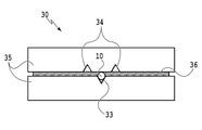
- FIG. 1 is a diagram showing an outline of an upper surface of an optical module according to an embodiment of the present invention.
- FIG. 2 is a perspective view and a bird's-eye view of the fiber block in the optical module according to the embodiment of the present invention.
- FIG. 3 is a diagram showing an outline of an end face of a fiber block in an optical module according to an embodiment of the present invention.
- FIG. 4 is a diagram showing a state of formation of a glass layer at a connection end face of a fiber block in a general optical module.
- FIG. 5 is a diagram showing a state of formation of a glass layer on a connection end face of a fiber block in an optical module according to an embodiment of the present invention.
- FIG. 6 is a diagram showing an outline of a connection end face of a fiber block configured by using a capillary in an optical module according to a modified embodiment of the present invention.
- FIG. 7 is a diagram showing an outline of a high power resistance measurement system in an optical module according to an embodiment of the present invention.
- FIG. 8 is a diagram showing a measurement result of loss fluctuation of the optical module according to the embodiment of the present invention.
- FIG. 9 is a diagram showing an outline of a connection end face of a planar light wave circuit in an optical module according to another embodiment of the present invention.
- FIG. 10 is a diagram showing an outline of a connection end surface of a planar light wave circuit in an optical module according to a modified embodiment of another embodiment of the present invention.
- the waveguide included in the PLC also referred to as a first waveguide
- the waveguide different from the first waveguide also referred to as a second waveguide
- An optical module optically connected via a layer is illustrated.
- the glass layer is the light input or output between the first waveguide and the second waveguide in the gap between the connecting end face of the first waveguide and the connecting end face of the second waveguide. It is provided in the area including at least the portion through which the light passes.
- the optical module comprises one or more tubules, one end of which is located in that region of the gap.
- the second waveguide may be an optical fiber inserted and fixed in a fiber block (ie, the PLC waveguide and the optical fiber are optically connected), or the PLC on which the first waveguide is formed. It may be a waveguide formed on a PLC different from the above (that is, the waveguides formed on the two PLCs are optically connected to each other).
- the PLC may be equipped with a yatoi plate.
- One or more tubules may be formed on at least one of the components of the fiber block or PLC or Yatoi plate.
- FIG. 1 shows an outline of the upper surface of the optical module according to the first embodiment of the present invention.
- This embodiment exemplifies an optical module in which a PLC waveguide and an optical fiber are optically connected.
- the optical module shown in FIG. 1 is between an optical fiber 10, a fiber block 30 into which the optical fiber 10 is inserted and fixed, a PLC 20 connected to the optical fiber 10, and a connection end surface of the PLC 20 and a connection end surface of the fiber block 30.
- the PLC 20 includes a waveguide 21 made on the substrate.
- the optical fiber 10 and the waveguide 21 are aligned so as to be optically coupled (optically coupled), and the PLC 20 and the fiber block 30 are bonded and fixed.
- the fiber block 30 includes two glass substrates 35 (for example, a V-groove substrate).
- the fiber block 30 has two glass substrates 35, an optical fiber 10 inserted and fixed between the two glass substrates 35, and an adhesive layer 36 for bonding the two glass substrates 35 to each other. Be prepared.
- a V-groove 33 for fixing the optical fiber 10 is formed on one of the two glass substrates 35.
- Two V-grooves 34 are formed on the other of the two glass substrates 35.
- the two V-grooves 34 form a thin tube.
- the V-groove 33 and the V-groove 34 are each formed on opposite surfaces of the two glass substrates 35.
- FIG. 2 shows a perspective view and a bird's-eye view of the fiber block 30 in the optical module according to the present embodiment.
- the fiber block 30 is generally formed by laminating two or more glass substrates 35 and sandwiching the optical fiber 10 (or inserting the optical fiber 10 between the two glass substrates 35). It has a structure for fixing, and has a structure in which a V groove 33 is carved (that is, formed) in one of two glass substrates 35 for fixing the optical fiber 10.
- the fiber block 30 is assembled by fitting (or inserting) the optical fiber 10 into the V-groove 33 and fixing it with an adhesive.
- the fiber block 30 is formed by digging a V-groove 45 extending from the connection end face to the other end face in the other glass substrate 35 different from the glass substrate 35 in which the V-groove 33 is carved.
- the V-groove 45 provides a thin tube extending in the longitudinal direction of the optical fiber 10.
- One V-groove 33 may be carved on each of the two opposing surfaces of the two glass substrates 35, and the optical fiber 10 may be fitted between the two V-grooves 33 and fixed with an adhesive.
- two V-grooves 34 and one V-groove 33 between the two V-grooves 34 may be carved on the upper glass substrate 35 of FIG.
- only one of the two glass substrates 35 may be carved with two V-grooves 34 and one V-groove 33 between the two V-grooves 34. good.
- FIG. 3 schematically shows the end face of the fiber block 30 of the present embodiment.
- two thin tubes V-grooves 34 described above are provided, and are arranged so as to sandwich the optical fiber 10.
- two thin tubes are provided in the fiber block 30, but at least one is sufficient. Further, the thin tube does not have to be parallel to the optical fiber 10.
- One end of the thin tube provided in the fiber block 30 is on the end face of the fiber block 30 (the end face of the connection facing the PLC), and the other end is on the other end face of the fiber block 30 (the end face other than the connection end face facing the PLC). It may be a structure.
- the V-groove 34 may be carved so that the thin tube branches and extends to a plurality of other ends.
- the outside air is passed through the thin tube at the connection point between the fiber block 30 and the PLC 20 (that is, the position where the optical fiber 10 and the waveguide 21 face each other (the optical or optical axis is). It can be introduced at the passing position) and its surroundings).
- a thin tube penetrating the fiber block 30 is provided by digging a V groove 34 in the glass substrate 35 constituting the fiber block 30, but a thin tube is provided in the fiber block 30 by providing a through hole by machining. You may.
- the UV curable resin adhesive layer 31 is provided so as not to straddle the optical axis so as not to be deteriorated by the light input / output between the optical fiber 10 and the waveguide 21 of the PLC 20. It is provided in the area other than the area through which the optical axis passes and its surroundings). In the present embodiment, the distance between the optical fiber 10 of the optical connection portion and the waveguide 21 of the PLC 20 is kept constant and the filling amount of the adhesive is controlled to prevent the resin from flowing out to the optical axis. If a sufficient area of the end face of the fiber block 30 can be secured, a groove for damming the adhesive may be provided on the end face of the fiber block 30 as shown in Patent Document 2.
- the glass layer 32 is provided so as to cover the optical axis at the connection point between the optical fiber 10 and the waveguide 21 of the PLC 20 (that is, at and around the position where the optical fiber 10 and the waveguide 21 face each other).
- the optical fiber 10 and the waveguide 21 of the PLC 20 are optically connected via the glass layer 32. Therefore, it is possible to suppress the dust collecting effect as shown in Patent Document 2 and suppress the increase in loss of the optical connection point with time.
- the glass layer 32 is produced by a liquid phase synthesis method.
- a liquid phase synthesis method for example, it is a kind of a sol-gel method or a sol-gel method in which a liquid raw material is polymerized to form a gel and then left at room temperature or baked to be cured to form a glass.
- a method using polysilazane to form glass by allowing polysilazane to stand at room temperature or baking it, or a liquid phase precipitation method using polysilazane to cure by hydrolyzing a liquid raw material to form glass can be used.
- polysilazane can be used as the precursor material of the glass layer 32. The following is a brief description of polysilazane.
- Polysilazane is an inorganic polymer material containing SiH2NH as a basic unit, and is cured by reacting with water to form a high-purity silica film.
- the cured silica film is colorless and transparent, has no absorption edge for visible light, and has high transparency.
- polysilazane becomes inorganic SiO 2 after curing, it has resistance to high-energy light and also has heat resistance of about 1000 ° C.
- polysilazane is a one-component type solution, it can be easily filled even in a minute gap at a connection point between the optical fiber 10 and the waveguide 21 of the PLC 20.
- polysilazane was used as the glass precursor, but one containing silicon alcoholic Si (OC2H5) 4 as a main component, one containing hydrogen silicate (H2SiF6) as a main component, or the like can be used.
- the waveguide 21 of the optical fiber 10 and the PLC 20 can be fixed so as not to cause an optical axis shift by providing the glass layer 32 having a sufficient area at the connection point, the UV curable resin adhesive layer 31 described above is provided. It does not have to be.
- the PLC 20 can be manufactured, for example, by the following procedure.
- An underclad layer made of quartz glass having a thickness of 20 ⁇ m and a core layer made of quartz glass having a thickness of 2 ⁇ m whose refractive index is increased by Ge-doping are sequentially deposited on a Si substrate.
- the core layer is formed into the pattern of the waveguide 21 by general exposure development technology and etching technology.
- the wafer is cut and a chip having a height of 5 mm and a width of 10 mm is cut out.
- the PLC 20 is completed by the above procedure, but in order to expand the bonding area with the fiber block 30, a SiO 2 substrate (Yatoi plate 90) having a height of 5 mm, a width of 2 mm, and a thickness of 1 mm is attached to the end of the PLC 20 chip to be bonded to the fiber block 30.
- a SiO 2 substrate (Yatoi plate 90) having a height of 5 mm, a width of 2 mm, and a thickness of 1 mm is attached to the end of the PLC 20 chip to be bonded to the fiber block 30.
- a UV curable resin adhesive was bonded with a UV curable resin adhesive.
- the fiber block 30 can be manufactured, for example, by the following procedure. First, two glass substrates 35 (SiO 2 substrate) having a thickness of 1 mm and an area of 5 mm ⁇ 5 mm are prepared. A V-groove 34 for fixing a fiber having a diameter of 125 ⁇ m is formed on one of the glass substrates 35 by machining, and the optical fiber 10 is fitted into the V-groove 34. The optical fiber 10 is sandwiched between another glass substrate 35, and the two glass substrates 35 and the optical fiber 10 sandwiched between these glass substrates 35 are bonded with a UV curable resin adhesive (UV curable resin adhesive). The layer 31 is formed), and finally the end face of the fiber block 30 is polished.
- a UV curable resin adhesive UV curable resin adhesive
- the conventional fiber block 30 is completed by the above procedure, but the fiber block 30 in the present embodiment is used to fix the optical fiber 10 before laminating the two glass substrates 35 (SiO 2 substrate).
- Two V-grooves 34 for introducing outside air are formed by machining on the other glass substrate 35 different from the glass substrate 35 on which the V-groove 33 is carved.
- the two V-grooves 34 are formed so as to be symmetrical with respect to the optical fiber 10 when the two glass substrates 35 are stacked and bonded as described above. It is necessary to adjust the coating amount of the adhesive used for bonding the glass substrates 35 and the pressing pressure at the time of bonding so that the two V-grooves 34 are not filled with the UV curable resin adhesive.
- the PLC 20 and the fiber block 30 manufactured as described above are fixed to the fine adjustment centering device, and the connection position is adjusted with the connection end face of the PLC 20 and the connection end face of the fiber block 30 separated by about 1 ⁇ m, and then UV curing is performed.
- the PLC 20 and the fiber block 30 are bonded and fixed using a resin adhesive. Adhesion and fixing with the UV curable resin adhesive are performed in a portion where the input or output light does not pass between the optical fiber 10 and the waveguide 21 of the PLC 20. Therefore, a gap is formed in the portion through which the light input or output passes between the optical fiber 10 and the waveguide 21 of the PLC 20.
- polysilazane which is a glass precursor, is placed in the gap of the light passing portion between the connection end face of the PLC 20 and the connection end face of the fiber block 30.
- the polysilazane is cured by filling and allowing it to stand at room temperature for several days to form a glass layer 37 in the light-passing portion.
- the optical module of the present embodiment was produced.
- FIG. 4 shows the formation of the glass layer 37 on the connection end face of the fiber block 30 in a general optical module
- FIG. 5 shows the glass layer on the connection end face of the fiber block 30 in the optical module according to the embodiment of the present invention.
- the state of formation is shown.
- the glass layer 37 shows a portion where polysilazane is hardened (hatched portion), and the inside thereof shows a portion where polysilazane is not hardened (hatched portion).
- FIGS. 4 and 5 show an example in which only polysilazane is used without using a UV curable resin adhesive when adhering and fixing the PLC 20 and the fiber block 30.
- the UV curable resin adhesive layer 31 is formed in a portion through which light does not pass, as described above.
- the end portion of the thin tube is provided by providing the thin tube (V groove 34) for introducing the outside air (that is, the optical fiber 10). Since the curing of polysilazane also starts from the position near the end), the glass layer 37 (SiO 2) is also filled (formed) in the optical connection portion (light passing portion) of the waveguide 21 of the optical fiber 10 and the PLC 20. Ru).
- the position where the end portion of the thin tube should be arranged depends on the area of the connection end surface of the fiber block 30, but in the fiber block 30 shape as shown in the present embodiment, from the optical connection portion (end portion of the optical fiber 10). It is effective to arrange it within 600 ⁇ m.
- two V-grooves 34 for introducing outside air are arranged so as to sandwich the optical fiber 10, so that the glass layer 37 formed by the curing shrinkage of polysilazane is symmetrical with respect to the optical connection point. This is to make the force applied to the PLC 20 and the fiber block 30 uniform in the process of curing and shrinking polysilazane.
- the glass layer 37 is asymmetrically formed at the optical connection point, there is a concern that the optical axis may shift in the process of hardening and shrinking of polysilazane. Therefore, in this embodiment, two thin tubes (V-grooves 34) are provided.
- the fiber block 30 in which two glass substrates 35 (SiO 2 substrate) are laminated is used, but as an alternative, a capillary provided with a plurality of capillaries may be used.
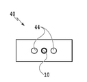
- FIG. 6 shows an outline of the connection end face of the capillary 40 constituting the fiber block 30 in the optical module according to the modified embodiment of the present invention.
- a capillary 40 having a plurality of capillaries 44 (three in FIG. 6) is prepared, and the optical fiber 10 is inserted into one of the plurality of capillaries 44 (the central capillary in FIG. 6).
- Any of the remaining capillaries 44 (two capillaries on the left and right in FIG. 6) can be used as the capillaries for introducing outside air.
- the thin tubes 44 used for introducing the outside air may be located on both sides of the thin tubes into which the optical fibers 10 are inserted so as to be close to the optical connection point and symmetrical. Since the optical fiber 10 and the PLC 20 can be bonded with a smaller bonding area than the fiber block 30, it is effective to configure the fiber block 30 by using the capillary 40 when sufficient bonding strength can be secured.
- FIG. 7 shows a high power resistance measurement system 70 for the optical module according to the present embodiment.
- light having a wavelength of 405 nm is incident from the input end of the optical module 50 from the input end of the optical module 50 via the optical fiber 10 inserted and fixed to the fiber block 30 connected to the PLC 20, and the optical module 50 is used.
- the output power of the light emitted from the output end of the above was measured by an optical power meter 72.
- the insertion loss of the entire optical module was 3.0 dB. Since the transmission loss of the PLC 20 is estimated to be 1.0 dB from the existing measurement, the connection loss at the two input / output ends is considered to be 1.0 dB, respectively.
- connection loss was 1.0 dB, which was the same as the measurement result of the embodiment. Therefore, it was confirmed that even if polysilazane is filled in the light passing portion, there is no problem in light transmission and a connection with low loss can be realized.
- FIG. 8 shows the result when the loss fluctuation of the optical module according to the present embodiment was continuously measured for 2000 hours when light having a wavelength of 405 nm and 20 mW was incident. As shown in FIG. 8, in the optical module according to the present embodiment, it was found that the insertion loss did not change from 3 dB even after 2000 hours.
- the optical module according to the present embodiment using polysilazane can withstand the reliability test. From this, when the optical fiber 10 and the waveguide 21 of the PLC 20 are optically connected by using polysilazane as in the present embodiment, it is possible to perform an optical connection that is resistant to high-energy light in the visible region. Shown.
- a second embodiment of the present invention relates to an optical module in which the waveguides 21 of two planar lightwave circuits (PLCs) 20 are optically connected to each other using polysilazane, and a method for producing the same.
- PLCs planar lightwave circuits
- FIG. 9 shows an overview of the connection end face of the PLC 20 in the optical module of the present embodiment.
- the yatoi plate 90 is adhered to each PLC 20.
- At least one of the two facing Yatoi plates 90 has two V-grooves 34 dug in a surface facing the PLC 20.
- the V-groove 34 constitutes a thin tube for introducing outside air in a state where the yatoi plate 90 is adhered to the PLC 20.
- One end of the thin tube is on the connecting end face of the yatoi plate 90, and the other end is on the other end face of the yatoi plate 90 (end face other than the connecting end face).
- the V-groove 34 may be carved so that the thin tube branches and extends to a plurality of other ends. At the connecting end faces of the yatoi plate 90 and the PCL 20, one end of the two thin tubes is located close to and symmetrical to the waveguide 21 of the PLC 20.
- the optical module of this embodiment can be manufactured by aligning, adhering and fixing two PLC20s to which a yatoi plate 90 is adhered, as described in the first embodiment. ..
- the connection loss at the optical connection point between the PLCs was 1.0 dB, which was equivalent to that of the first embodiment. Further, in order to evaluate the high power resistance of the optical connection portion, light having a wavelength of 405 nm and 1 mW was continuously transmitted to the optical module for 2000 hours, but the insertion loss fluctuated. Therefore, the optical module of the present embodiment can also realize an optical connection having high power resistance as in the first embodiment.
- two PLC20s can be directly bonded and fixed without an optical fiber, and the optical connection point thereof is resistant to high-power light, and a small module that is less likely to cause axial misalignment even in a high temperature environment. Can be realized. Further, as compared with the case where two PLCs are connected to each other via an optical fiber, the optical module of the present embodiment has half the number of optical connection points, which contributes to improvement of yield and cost reduction.
- a thin tube for introducing outside air is provided by digging a V groove 34 in the yatoi plate, but as a modified form of the present embodiment, a deep groove is formed when the PLC 20 is manufactured. It may be dug or a thin tube may be provided.
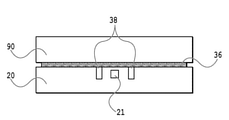
- FIG. 10 shows an outline of the connection end face of the plane light wave circuit in the optical module according to the modified form of the present embodiment.
- a deep groove 38 is dug in the surface of the PLC 20 facing the yatoi plate 90, and the deep groove 38 constitutes a thin tube for introducing outside air in a state where the yatoi plate 90 is adhered to the PLC 20. You may do so. If there is a process of digging a groove by dry etching or the like at the time of manufacturing the PLC 20, it is possible to dig a deep groove 38 for introducing outside air at the same time, and it is possible to reduce the process load.
- one end of the two thin tubes is on the connecting end face of the PLC 20, and the other end is on the other end face of the PLC 20 (end face other than the connecting end face).
- the deep groove 38 may be carved so that the thin tube branches and extends to a plurality of other ends.
- one end of the two thin tubes is located close to and symmetrical to the waveguide 21 of the PLC 20.
- the optical module of FIG. 10 can also be manufactured by aligning, adhering and fixing two PLC20s to which a yatoi plate 90 is adhered, respectively, as described in the first embodiment.
- An optical module can also be manufactured by aligning, adhering, and fixing the connection end face of the fiber block 30 into which the optical fiber 10 is inserted and fixed. Alternatively, it does not have the connection end face of the PLC20 to which the Yatoi plate 90 described with reference to FIGS. 9 and 10 is bonded and the general thin tube described with reference to FIG. 4 (V-groove 34 is not formed). An optical module can also be manufactured by aligning, adhering, and fixing the connection end face of the fiber block 30 into which the optical fiber 10 is inserted and fixed.
- outside air is supplied to the optical connection point by the thin tube provided in the fiber block, and the generation of voids due to the hardening shrinkage of polysilazane is suppressed on the optical axis. do.
- SiO 2 As a result, it becomes possible to efficiently fill the optical axis with SiO 2, and it becomes possible to provide an optical module resistant to high-energy light with a high yield.
Landscapes
- Physics & Mathematics (AREA)
- General Physics & Mathematics (AREA)
- Optics & Photonics (AREA)
- Optical Couplings Of Light Guides (AREA)
Abstract
L'invention concerne un module optique comprenant un circuit d'onde lumineuse plane qui est optiquement connecté à une fibre optique, un bloc de fibres auquel la fibre optique est fixée, et une couche de verre qui lie et fixe le bloc de fibres et le circuit d'onde de lumière plane. La couche de verre est disposée sur une partie à travers laquelle la lumière passe entre la fibre optique et le circuit d'onde lumineuse plane, ladite partie étant située dans un espace entre une surface d'extrémité de connexion du bloc de fibres et une surface d'extrémité de connexion du circuit d'onde de lumière plane. Le module optique comprend en outre un tube fin. Le tube fin peut être disposé de façon à passer à travers le bloc de fibres. Le tube fin peut être disposé de façon à passer à travers le circuit d'onde lumineuse plane ou à travers une plaque de protection montée sur le circuit d'onde lumineuse plane.
Priority Applications (3)
| Application Number | Priority Date | Filing Date | Title |
|---|---|---|---|
| PCT/JP2020/028177 WO2022018816A1 (fr) | 2020-07-20 | 2020-07-20 | Module optique |
| JP2022538521A JP7372578B2 (ja) | 2020-07-20 | 2020-07-20 | 光モジュール |
| US18/004,811 US20230251432A1 (en) | 2020-07-20 | 2020-07-20 | Optical Module |
Applications Claiming Priority (1)
| Application Number | Priority Date | Filing Date | Title |
|---|---|---|---|
| PCT/JP2020/028177 WO2022018816A1 (fr) | 2020-07-20 | 2020-07-20 | Module optique |
Publications (1)
| Publication Number | Publication Date |
|---|---|
| WO2022018816A1 true WO2022018816A1 (fr) | 2022-01-27 |
Family
ID=79729136
Family Applications (1)
| Application Number | Title | Priority Date | Filing Date |
|---|---|---|---|
| PCT/JP2020/028177 WO2022018816A1 (fr) | 2020-07-20 | 2020-07-20 | Module optique |
Country Status (3)
| Country | Link |
|---|---|
| US (1) | US20230251432A1 (fr) |
| JP (1) | JP7372578B2 (fr) |
| WO (1) | WO2022018816A1 (fr) |
Cited By (2)
| Publication number | Priority date | Publication date | Assignee | Title |
|---|---|---|---|---|
| EP4231070A1 (fr) * | 2022-02-16 | 2023-08-23 | Honeywell International Inc. | Procédés de couplage de fibre à puce utilisant des matériaux d'adaptation d'indice coulants |
| WO2024105765A1 (fr) * | 2022-11-15 | 2024-05-23 | 日本電信電話株式会社 | Module optique et procédé de production de module optique |
Citations (5)
| Publication number | Priority date | Publication date | Assignee | Title |
|---|---|---|---|---|
| JPS63237004A (ja) * | 1987-03-26 | 1988-10-03 | Seiko Instr & Electronics Ltd | 光フアイバと光導波路の接続方法 |
| US6526204B1 (en) * | 2000-07-11 | 2003-02-25 | Shipley Company Llc | Optical fiber array for preventing flow of glue between fibers and waveguide |
| JP2004334003A (ja) * | 2003-05-09 | 2004-11-25 | Hitachi Printing Solutions Ltd | 光結合素子の製造法及び光記録装置 |
| JP2005215426A (ja) * | 2004-01-30 | 2005-08-11 | Ricoh Printing Systems Ltd | 半導体レーザモジュール |
| JP2018194802A (ja) * | 2017-05-22 | 2018-12-06 | 日本電信電話株式会社 | 光モジュールおよびその作製方法 |
-
2020
- 2020-07-20 WO PCT/JP2020/028177 patent/WO2022018816A1/fr active Application Filing
- 2020-07-20 JP JP2022538521A patent/JP7372578B2/ja active Active
- 2020-07-20 US US18/004,811 patent/US20230251432A1/en active Pending
Patent Citations (5)
| Publication number | Priority date | Publication date | Assignee | Title |
|---|---|---|---|---|
| JPS63237004A (ja) * | 1987-03-26 | 1988-10-03 | Seiko Instr & Electronics Ltd | 光フアイバと光導波路の接続方法 |
| US6526204B1 (en) * | 2000-07-11 | 2003-02-25 | Shipley Company Llc | Optical fiber array for preventing flow of glue between fibers and waveguide |
| JP2004334003A (ja) * | 2003-05-09 | 2004-11-25 | Hitachi Printing Solutions Ltd | 光結合素子の製造法及び光記録装置 |
| JP2005215426A (ja) * | 2004-01-30 | 2005-08-11 | Ricoh Printing Systems Ltd | 半導体レーザモジュール |
| JP2018194802A (ja) * | 2017-05-22 | 2018-12-06 | 日本電信電話株式会社 | 光モジュールおよびその作製方法 |
Cited By (2)
| Publication number | Priority date | Publication date | Assignee | Title |
|---|---|---|---|---|
| EP4231070A1 (fr) * | 2022-02-16 | 2023-08-23 | Honeywell International Inc. | Procédés de couplage de fibre à puce utilisant des matériaux d'adaptation d'indice coulants |
| WO2024105765A1 (fr) * | 2022-11-15 | 2024-05-23 | 日本電信電話株式会社 | Module optique et procédé de production de module optique |
Also Published As
| Publication number | Publication date |
|---|---|
| JP7372578B2 (ja) | 2023-11-01 |
| US20230251432A1 (en) | 2023-08-10 |
| JPWO2022018816A1 (fr) | 2022-01-27 |
Similar Documents
| Publication | Publication Date | Title |
|---|---|---|
| JP3984009B2 (ja) | 光導波路デバイスの製造方法 | |
| KR0139133B1 (ko) | 광파이버와 광도파로의 결합구조 | |
| US4765702A (en) | Glass integrated optical component | |
| US5042896A (en) | Polarization device | |
| WO2022018816A1 (fr) | Module optique | |
| JP6767925B2 (ja) | 光モジュールおよびその作製方法 | |
| CN113467111A (zh) | 光波导元件 | |
| WO2021100150A1 (fr) | Module optique | |
| WO2022038763A1 (fr) | Module optique | |
| JP7124672B2 (ja) | 光接続部品および光接続構造 | |
| JP7464053B2 (ja) | 光導波路素子のアライメント方法 | |
| JP3450068B2 (ja) | 光導波路の結合構造 | |
| JP4012537B2 (ja) | 光モジュール及びその作製方法 | |
| JP7124632B2 (ja) | 光接続構造およびその形成方法 | |
| JPH0534543A (ja) | 導波型光部品 | |
| JP3279438B2 (ja) | 光ファイバと光導波路の結合構造 | |
| JP4018852B2 (ja) | 光導波路基板 | |
| WO2023079720A1 (fr) | Élément optique, élément optique intégré et procédé de fabrication d'élément optique intégré | |
| JP3163580B2 (ja) | 導波型光部品 | |
| WO2024105765A1 (fr) | Module optique et procédé de production de module optique | |
| JP7244788B2 (ja) | 光ファイバ接続構造 | |
| JP4303096B2 (ja) | 平面光回路部品 | |
| JP3681439B2 (ja) | 光導波路と光ファイバの接続方法 | |
| JP2002107564A (ja) | 光導波路モジュール | |
| JP3430501B2 (ja) | 光導波路デバイスおよびその製造方法 |
Legal Events
| Date | Code | Title | Description |
|---|---|---|---|
| 121 | Ep: the epo has been informed by wipo that ep was designated in this application |
Ref document number: 20946156 Country of ref document: EP Kind code of ref document: A1 |
|
| ENP | Entry into the national phase |
Ref document number: 2022538521 Country of ref document: JP Kind code of ref document: A |
|
| NENP | Non-entry into the national phase |
Ref country code: DE |
|
| 122 | Ep: pct application non-entry in european phase |
Ref document number: 20946156 Country of ref document: EP Kind code of ref document: A1 |