WO2022014623A1 - 半導体装置 - Google Patents
半導体装置 Download PDFInfo
- Publication number
- WO2022014623A1 WO2022014623A1 PCT/JP2021/026375 JP2021026375W WO2022014623A1 WO 2022014623 A1 WO2022014623 A1 WO 2022014623A1 JP 2021026375 W JP2021026375 W JP 2021026375W WO 2022014623 A1 WO2022014623 A1 WO 2022014623A1
- Authority
- WO
- WIPO (PCT)
- Prior art keywords
- region
- concentration
- peak
- semiconductor device
- collector
- Prior art date
- Legal status (The legal status is an assumption and is not a legal conclusion. Google has not performed a legal analysis and makes no representation as to the accuracy of the status listed.)
- Ceased
Links
Images










Classifications
-
- H—ELECTRICITY
- H10—SEMICONDUCTOR DEVICES; ELECTRIC SOLID-STATE DEVICES NOT OTHERWISE PROVIDED FOR
- H10D—INORGANIC ELECTRIC SEMICONDUCTOR DEVICES
- H10D62/00—Semiconductor bodies, or regions thereof, of devices having potential barriers
- H10D62/10—Shapes, relative sizes or dispositions of the regions of the semiconductor bodies; Shapes of the semiconductor bodies
- H10D62/13—Semiconductor regions connected to electrodes carrying current to be rectified, amplified or switched, e.g. source or drain regions
- H10D62/137—Collector regions of BJTs
-
- H—ELECTRICITY
- H10—SEMICONDUCTOR DEVICES; ELECTRIC SOLID-STATE DEVICES NOT OTHERWISE PROVIDED FOR
- H10D—INORGANIC ELECTRIC SEMICONDUCTOR DEVICES
- H10D62/00—Semiconductor bodies, or regions thereof, of devices having potential barriers
- H10D62/10—Shapes, relative sizes or dispositions of the regions of the semiconductor bodies; Shapes of the semiconductor bodies
- H10D62/124—Shapes, relative sizes or dispositions of the regions of semiconductor bodies or of junctions between the regions
- H10D62/126—Top-view geometrical layouts of the regions or the junctions
- H10D62/127—Top-view geometrical layouts of the regions or the junctions of cellular field-effect devices, e.g. multicellular DMOS transistors or IGBTs
-
- H—ELECTRICITY
- H10—SEMICONDUCTOR DEVICES; ELECTRIC SOLID-STATE DEVICES NOT OTHERWISE PROVIDED FOR
- H10D—INORGANIC ELECTRIC SEMICONDUCTOR DEVICES
- H10D12/00—Bipolar devices controlled by the field effect, e.g. insulated-gate bipolar transistors [IGBT]
- H10D12/01—Manufacture or treatment
- H10D12/031—Manufacture or treatment of IGBTs
- H10D12/032—Manufacture or treatment of IGBTs of vertical IGBTs
- H10D12/038—Manufacture or treatment of IGBTs of vertical IGBTs having a recessed gate, e.g. trench-gate IGBTs
-
- H—ELECTRICITY
- H10—SEMICONDUCTOR DEVICES; ELECTRIC SOLID-STATE DEVICES NOT OTHERWISE PROVIDED FOR
- H10D—INORGANIC ELECTRIC SEMICONDUCTOR DEVICES
- H10D12/00—Bipolar devices controlled by the field effect, e.g. insulated-gate bipolar transistors [IGBT]
- H10D12/411—Insulated-gate bipolar transistors [IGBT]
- H10D12/441—Vertical IGBTs
- H10D12/461—Vertical IGBTs having non-planar surfaces, e.g. having trenches, recesses or pillars in the surfaces of the emitter, base or collector regions
- H10D12/481—Vertical IGBTs having non-planar surfaces, e.g. having trenches, recesses or pillars in the surfaces of the emitter, base or collector regions having gate structures on slanted surfaces, on vertical surfaces, or in grooves, e.g. trench gate IGBTs
-
- H—ELECTRICITY
- H10—SEMICONDUCTOR DEVICES; ELECTRIC SOLID-STATE DEVICES NOT OTHERWISE PROVIDED FOR
- H10D—INORGANIC ELECTRIC SEMICONDUCTOR DEVICES
- H10D62/00—Semiconductor bodies, or regions thereof, of devices having potential barriers
- H10D62/10—Shapes, relative sizes or dispositions of the regions of the semiconductor bodies; Shapes of the semiconductor bodies
- H10D62/102—Constructional design considerations for preventing surface leakage or controlling electric field concentration
- H10D62/112—Constructional design considerations for preventing surface leakage or controlling electric field concentration for preventing surface leakage due to surface inversion layers, e.g. by using channel stoppers
-
- H—ELECTRICITY
- H10—SEMICONDUCTOR DEVICES; ELECTRIC SOLID-STATE DEVICES NOT OTHERWISE PROVIDED FOR
- H10D—INORGANIC ELECTRIC SEMICONDUCTOR DEVICES
- H10D62/00—Semiconductor bodies, or regions thereof, of devices having potential barriers
- H10D62/10—Shapes, relative sizes or dispositions of the regions of the semiconductor bodies; Shapes of the semiconductor bodies
- H10D62/13—Semiconductor regions connected to electrodes carrying current to be rectified, amplified or switched, e.g. source or drain regions
- H10D62/141—Anode or cathode regions of thyristors; Collector or emitter regions of gated bipolar-mode devices, e.g. of IGBTs
- H10D62/142—Anode regions of thyristors or collector regions of gated bipolar-mode devices
-
- H—ELECTRICITY
- H10—SEMICONDUCTOR DEVICES; ELECTRIC SOLID-STATE DEVICES NOT OTHERWISE PROVIDED FOR
- H10D—INORGANIC ELECTRIC SEMICONDUCTOR DEVICES
- H10D62/00—Semiconductor bodies, or regions thereof, of devices having potential barriers
- H10D62/10—Shapes, relative sizes or dispositions of the regions of the semiconductor bodies; Shapes of the semiconductor bodies
- H10D62/17—Semiconductor regions connected to electrodes not carrying current to be rectified, amplified or switched, e.g. channel regions
- H10D62/393—Body regions of DMOS transistors or IGBTs
-
- H—ELECTRICITY
- H10—SEMICONDUCTOR DEVICES; ELECTRIC SOLID-STATE DEVICES NOT OTHERWISE PROVIDED FOR
- H10D—INORGANIC ELECTRIC SEMICONDUCTOR DEVICES
- H10D62/00—Semiconductor bodies, or regions thereof, of devices having potential barriers
- H10D62/60—Impurity distributions or concentrations
-
- H—ELECTRICITY
- H10—SEMICONDUCTOR DEVICES; ELECTRIC SOLID-STATE DEVICES NOT OTHERWISE PROVIDED FOR
- H10D—INORGANIC ELECTRIC SEMICONDUCTOR DEVICES
- H10D8/00—Diodes
- H10D8/422—PN diodes having the PN junctions in mesas
-
- H—ELECTRICITY
- H10—SEMICONDUCTOR DEVICES; ELECTRIC SOLID-STATE DEVICES NOT OTHERWISE PROVIDED FOR
- H10D—INORGANIC ELECTRIC SEMICONDUCTOR DEVICES
- H10D62/00—Semiconductor bodies, or regions thereof, of devices having potential barriers
- H10D62/50—Physical imperfections
- H10D62/53—Physical imperfections the imperfections being within the semiconductor body
-
- H—ELECTRICITY
- H10—SEMICONDUCTOR DEVICES; ELECTRIC SOLID-STATE DEVICES NOT OTHERWISE PROVIDED FOR
- H10D—INORGANIC ELECTRIC SEMICONDUCTOR DEVICES
- H10D64/00—Electrodes of devices having potential barriers
- H10D64/111—Field plates
- H10D64/117—Recessed field plates, e.g. trench field plates or buried field plates
-
- H—ELECTRICITY
- H10—SEMICONDUCTOR DEVICES; ELECTRIC SOLID-STATE DEVICES NOT OTHERWISE PROVIDED FOR
- H10D—INORGANIC ELECTRIC SEMICONDUCTOR DEVICES
- H10D64/00—Electrodes of devices having potential barriers
- H10D64/20—Electrodes characterised by their shapes, relative sizes or dispositions
- H10D64/27—Electrodes not carrying the current to be rectified, amplified, oscillated or switched, e.g. gates
- H10D64/311—Gate electrodes for field-effect devices
- H10D64/411—Gate electrodes for field-effect devices for FETs
- H10D64/511—Gate electrodes for field-effect devices for FETs for IGFETs
- H10D64/517—Gate electrodes for field-effect devices for FETs for IGFETs characterised by the conducting layers
- H10D64/519—Gate electrodes for field-effect devices for FETs for IGFETs characterised by the conducting layers characterised by their top-view geometrical layouts
-
- H—ELECTRICITY
- H10—SEMICONDUCTOR DEVICES; ELECTRIC SOLID-STATE DEVICES NOT OTHERWISE PROVIDED FOR
- H10D—INORGANIC ELECTRIC SEMICONDUCTOR DEVICES
- H10D84/00—Integrated devices formed in or on semiconductor substrates that comprise only semiconducting layers, e.g. on Si wafers or on GaAs-on-Si wafers
- H10D84/80—Integrated devices formed in or on semiconductor substrates that comprise only semiconducting layers, e.g. on Si wafers or on GaAs-on-Si wafers characterised by the integration of at least one component covered by groups H10D12/00 or H10D30/00, e.g. integration of IGFETs
- H10D84/811—Combinations of field-effect devices and one or more diodes, capacitors or resistors
Definitions
- the present invention relates to a semiconductor device.
- Patent Document 1 Japanese Patent Application Laid-Open No. 2015-135954
- a first conductive type drift region provided on the semiconductor substrate, a first conductive type field stop region provided below the drift region and having one or more peaks, and the like.
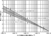
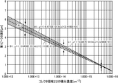
- a second conductive type collector region provided below the field stop region is provided, and the integrated concentration of the collector region is x [cm -2 ], and the shallowest of one or a plurality of peaks from the back surface of the semiconductor substrate. The depth of one peak is y1 [ ⁇ m].
- Line A1: y1 (-7.4699E-01) ln (x) + (2.7810E + 01)
- Line B1: y1 (-4.7772E-01) ln (x) + (1.7960E + 01)
- the integrated concentration in the collector region may be 8.00E15 cm-2 or less.
- the integrated concentration in the collector region may be 3.00E14 cm -2 or less.
- the integrated concentration in the collector region may be 2.00E 14 cm -2 or less.
- the integrated concentration in the collector region may be 1.00E14 cm -2 or less.
- the integrated concentration in the collector region may be 5.00E 13 cm -2 or less.
- the integrated concentration in the collector region may be 3.00E13 cm -2 or less.
- the integrated concentration in the collector region may be 1.00E 13 cm -2 or less.
- the depth of the first peak may be 0.5 ⁇ m or more and 7.2 ⁇ m or less.
- the depth of the first peak may be 2.0 ⁇ m or more and 7.2 ⁇ m or less.
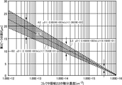
- the depth of the second peak which is the second shallowest from the back surface of one or more peaks, is y2 [ ⁇ m].
- Line A2: y2 (-3.1095E + 00) ln (x) + (1.1416E + 02)
- Line B2: y2 (-1.9239E + 00) ln (x) + (7.1030E + 01)
- the depth of the second peak and the integrated concentration may be in the range between the line A2 and the line B2.
- the depth of the second peak may be 3.5 ⁇ m or more and 28 ⁇ m or less.
- the stray inductance Ls of the circuit connected to the semiconductor device is Xc [nH], and the collector current reduction rate dIce / dt is Yc [A / ⁇ s].
- Line C1: Yc 10000Xc -1 ,
- the stray inductance Ls and the collector current reduction rate dIce / dt may be in a range larger than that of the line C1.
- the dopant for one or more peaks may be hydrogen.
- An active region provided on the semiconductor substrate and an outer peripheral region provided on the outer periphery of the active region in the top view of the semiconductor substrate may be provided.
- a second conductive type contact region having a higher doping concentration than the base region and a plurality of gate trench portions provided on the semiconductor substrate may be provided.
- the doping concentration at the boundary between the field stop region and the collector region may be 1E 16 cm -3 or less.
- the doping concentration at the boundary between the field stop region and the collector region may be 5E15 cm -3 or less.
- the doping concentration at the boundary between the field stop region and the collector region may be 2E15 cm -3 or less.
- the hydrogen chemical concentration at the boundary between the field stop region and the collector region may be 1E18 cm -3 or less.
- the hydrogen chemical concentration at the boundary between the field stop region and the collector region may be 1E17 cm -3 or less.
- the hydrogen chemical concentration at the boundary between the field stop region and the collector region may be 1E15 cm -3 or higher.
- the hydrogen chemical concentration at the boundary between the field stop region and the collector region may be 1E16 cm -3 or higher.
- FIG. 1A It is a figure which shows an example of the aa'cross section in FIG. 1A. This is an example of a circuit at the time of a clamp withstand voltage test of the semiconductor device 100. It is a figure for demonstrating the clamp energy of the semiconductor device 100. The relationship between the doping concentration of the collector region 22 and the clamping energy is shown. The relationship between the doping concentration of the collector region 22 and the withstand voltage of the device is shown. An example of the current-voltage characteristics of the semiconductor device 100 according to the embodiment is shown. An example of the current-voltage characteristics of the semiconductor device 500 according to the comparative example is shown. An example of the relationship between the integrated concentration of the collector region 22 and the depth of the first peak P1 is shown.
- Another example of the relationship between the integrated concentration of the collector region 22 and the depth of the first peak P1 is shown. Another example of the relationship between the integrated concentration of the collector region 22 and the depth of the first peak P1 is shown. Another example of the relationship between the integrated concentration of the collector region 22 and the depth of the first peak P1 is shown. Another example of the relationship between the integrated concentration of the collector region 22 and the depth of the first peak P1 is shown. Another example of the relationship between the integrated concentration of the collector region 22 and the depth of the first peak P1 is shown. Another example of the relationship between the integrated concentration of the collector region 22 and the depth of the first peak P1 is shown. Another example of the relationship between the integrated concentration of the collector region 22 and the depth of the first peak P1 is shown. Another example of the relationship between the integrated concentration of the collector region 22 and the depth of the first peak P1 is shown.
- Another example of the relationship between the integrated concentration of the collector region 22 and the depth of the first peak P1 is shown.
- the relationship between the integrated concentration of the collector region 22 and the depth of the second peak P2 is shown.
- Another example of the relationship between the integrated concentration of the collector region 22 and the depth of the second peak P2 is shown.
- the relationship between the integrated concentration of the collector region 22 and the depth of the second peak P2 is shown. It is a figure for demonstrating the relationship between a stray inductance Ls and a collector current reduction rate dIce / dt. It is a figure for demonstrating the relationship between the specific stray inductance Ls ⁇ A and the current density dJce / dt. It is a figure for demonstrating the relationship between the specific stray inductance Ls ⁇ A and the specific gate resistance Rg ⁇ A.
- one side in the direction parallel to the depth direction of the semiconductor substrate is referred to as "upper”, and the other side is referred to as “lower”.
- the upper surface is referred to as the upper surface and the other surface is referred to as the lower surface.
- the directions of "top”, “bottom”, “front”, and “back” are not limited to the direction of gravity or the direction of mounting on a substrate or the like when mounting a semiconductor device.
- orthogonal coordinate axes of X-axis, Y-axis, and Z-axis Orthogonal axes only specify the relative positions of the components and do not limit a particular direction.
- the Z axis does not limit the height direction with respect to the ground.
- the + Z-axis direction and the ⁇ Z-axis direction are opposite to each other. When positive or negative is not described and is described as the Z-axis direction, it means the direction parallel to the + Z-axis and the -Z-axis.
- the plane parallel to the upper surface of the semiconductor substrate is referred to as the XY plane, and the orthogonal axes parallel to the upper and lower surfaces of the semiconductor substrate are referred to as the X axis and the Y axis.
- the axis perpendicular to the upper surface and the lower surface of the semiconductor substrate is defined as the Z axis.
- the depth direction of the semiconductor substrate may be referred to as the Z axis.
- the case where the semiconductor substrate is viewed in the Z-axis direction is referred to as a plan view.
- the direction parallel to the upper surface and the lower surface of the semiconductor substrate including the X-axis and the Y-axis may be referred to as a horizontal direction.
- the first conductive type is N type and the second conductive type is P type, but the first conductive type may be P type and the second conductive type may be N type.
- the conductive types such as the substrate, the layer, and the region in each embodiment have opposite polarities.
- error When referred to as “same” or “equal” in the present specification, it may include a case where there is an error due to manufacturing variation or the like.
- the error is, for example, within 10%.
- the conductive type of the doping region doped with impurities is described as P type or N type.
- an impurity may mean, in particular, either an N-type donor or a P-type acceptor, and may be referred to as a dopant.
- doping means that a donor or acceptor is introduced into a semiconductor substrate to obtain a semiconductor showing an N-type conductive type or a semiconductor showing a P-type conductive type.
- the doping concentration means the concentration of a donor or the concentration of an acceptor in a thermal equilibrium state.
- the net doping concentration means the net concentration of the donor concentration as the concentration of positive ions and the acceptor concentration as the concentration of negative ions, including the polarity of the charge.
- the donor concentration N D, the acceptor concentration and N A, the net doping concentration of the net at any position is N D -N A.
- the donor has the function of supplying electrons to the semiconductor.
- the acceptor has a function of receiving electrons from a semiconductor.
- Donors and acceptors are not limited to the impurities themselves.
- the VOH defect to which the pores (V), oxygen (O) and hydrogen (H) present in the semiconductor are bonded functions as a donor for supplying electrons.
- VOH defects may be referred to simply as hydrogen donors.
- P + type or N + type means that the doping concentration is higher than P type or N type
- P-type or N-type means that the doping concentration is higher than P-type or N-type. It means that the concentration is low.
- P ++ type or N ++ type in the present specification it means that the doping concentration is higher than that of P + type or N + type.
- the chemical concentration refers to the atomic density of impurities measured regardless of the state of electrical activation.
- the chemical concentration can be measured, for example, by secondary ion mass spectrometry (SIMS).
- the net doping concentration described above can be measured by a voltage-capacity measurement method (CV method).
- the carrier concentration measured by the spread resistance measurement method (SR method) may be used as the net doping concentration.
- the carrier concentration measured by the CV method or the SR method may be a value in a thermal equilibrium state.
- the donor concentration is sufficiently higher than the acceptor concentration, so the carrier concentration in the region may be used as the donor concentration.
- the carrier concentration in the region may be used as the acceptor concentration.
- Each concentration in the present invention may be a value at room temperature. As the value at room temperature, the value at 300 K (Kelvin) (about 26.9 ° C.) may be used as an example.
- the peak value may be used as the concentration of the donor, acceptor or net doping in the region.
- the concentration of the donor, the acceptor or the net doping is substantially uniform, the average value of the concentration of the donor, the acceptor or the net doping in the region may be used as the concentration of the donor, the acceptor or the net doping.
- the carrier concentration measured by the SR method may be lower than the concentration of the donor or acceptor.
- the carrier mobility of the semiconductor substrate may be lower than the value in the crystalline state. The decrease in carrier mobility occurs when carriers are scattered due to disorder of the crystal structure due to lattice defects or the like.
- the concentration of the donor or acceptor calculated from the carrier concentration measured by the CV method or the SR method may be lower than the chemical concentration of the element indicating the donor or acceptor.
- the donor concentration of phosphorus or arsenic as a donor in a silicon semiconductor, or the acceptor concentration of boron (boron) as an acceptor is about 99% of these chemical concentrations.
- the donor concentration of hydrogen as a donor in a silicon semiconductor is, for example, about 0.1% to 10% of the chemical concentration of hydrogen.
- the unit system of this specification is an SI unit system unless otherwise specified.
- the unit of length may be displayed in cm or the like, but various calculations may be performed after converting to meters (m).
- the doping concentration refers to the concentration of a donor or accepted dopant.
- the unit is / cm 3.
- the concentration difference between the donor and the acceptor (that is, the net doping concentration) may be referred to as the doping concentration.
- the doping concentration can be measured by the SR method.
- the chemical concentration of the donor and the acceptor may be used as the doping concentration.
- the doping concentration can be measured by the SIMS method. Unless otherwise limited, any of the above may be used as the doping concentration. Unless otherwise limited, the peak value of the doping concentration distribution in the doping region may be used as the doping concentration in the doping region.
- the dose amount means the number of ions per unit area injected into the wafer when ion implantation is performed. Therefore, the unit is / cm 2 .
- the dose amount in the semiconductor region can be an integrated concentration obtained by integrating the doping concentration over the depth direction of the semiconductor region.
- the unit of the integrated concentration is / cm 2 . Therefore, the dose amount and the integrated concentration may be treated as the same.
- the integrated concentration may be an integrated value up to the full width at half maximum, and when it overlaps with the spectrum of another semiconductor region, it may be derived excluding the influence of the other semiconductor region.
- the high and low doping concentrations can be read as the high and low dose amounts. That is, when the doping concentration in one region is higher than the doping concentration in the other region, it can be understood that the dose amount in the one region is higher than the dose amount in the other region.
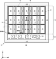
- FIG. 1A is an example of a top view of the semiconductor device 100.
- the semiconductor device 100 includes an active region 110, an outer peripheral region 120, and a pad region 130.
- the semiconductor device 100 is a semiconductor chip including a transistor unit 70 and a diode unit 80.
- the semiconductor device 100 includes a temperature sense unit 76 and may be mounted on a module such as an IPM (Intelligent Power Module).
- IPM Intelligent Power Module
- the transistor unit 70 includes a transistor such as an IGBT (Insulated Gate Bipolar Transistor).
- the diode section 80 includes a diode such as a freewheeling diode (FWD: Free Wheel Diode).
- the semiconductor device 100 of this example is a reverse conduction IGBT (RC-IGBT: Reverse Control IGBT) having a transistor portion 70 and a diode portion 80 on the same chip.
- the transistor of the transistor unit 70 is an IGBT.
- the semiconductor substrate 10 may be a silicon substrate, a silicon carbide substrate, a nitride semiconductor substrate such as gallium nitride, or the like.
- the semiconductor substrate 10 of this example is a silicon substrate.
- the semiconductor substrate 10 has an active region 110 and an outer peripheral region 120.
- the transistor portion 70 and the diode portion 80 may be alternately and periodically arranged periodically in the XY plane.
- the semiconductor device 100 of this example includes a plurality of transistor units 70 and a plurality of diode units 80, respectively.
- the transistor portion 70 and the diode portion 80 of this example have a trench portion extending in the Y-axis direction.
- the transistor portion 70 and the diode portion 80 may have a trench portion extending in the X-axis direction.
- the temperature sense unit 76 is provided above the active region 110.
- the temperature sense unit 76 may be formed of single crystal or polycrystalline silicon.
- the forward voltage of the current flowing through the temperature sense unit 76 changes.
- the temperature of the semiconductor device 100 can be detected based on the change in the forward voltage.
- the active region 110 has a transistor unit 70 and a diode unit 80.
- the active region 110 is a region in which a main current flows between the front surface and the back surface of the semiconductor substrate 10 when the semiconductor device 100 is controlled to be in the ON state. That is, it is a region in which a current flows in the depth direction inside the semiconductor substrate 10 from the front surface to the back surface of the semiconductor substrate 10 or from the back surface to the front surface.
- the transistor unit 70 and the diode unit 80 are referred to as element units or element regions, respectively.
- the region sandwiched between the two element portions is also referred to as the active region 110.
- the active region 110 also includes a region sandwiched between the element portions and provided with the gate runner 51.
- the gate runner 51 may supply the gate potential supplied from the gate pad 131 of the pad region 130 to the gate conductive portion of the transistor portion 70.
- the gate runner 51 is provided along the outer circumference of the active region 110 in top view.
- the gate runner 51 may also be provided in the region between the transistor portion 70 and the diode portion 80 in a top view.
- the outer peripheral region 120 is provided around the end portion of the semiconductor substrate 10 so as to surround the active region 110 and the pad region 130 in the top view. It is a region between the outer peripheral edge of the semiconductor substrate 10.
- the outer peripheral region 120 is provided so as to surround the active region 110 in top view.
- the outer peripheral region 120 may have an edge termination structure.
- the edge terminal structure portion relaxes the electric field concentration on the front surface side of the semiconductor substrate 10.
- the edge termination structure has a guard ring, a field plate, a resurf, and a combination thereof.
- the pad area 130 includes a gate pad 131, a sense IGBT 132, a sense emitter pad 133, an anode pad 134, and a cathode pad 135.
- the cathode pad 135, the anode pad 134, the gate pad 131, the sense IGBT 132, and the sense emitter pad 133 are provided side by side in this order in the X-axis direction.
- Each pad may be an electrode pad containing gold (Au), silver (Ag), copper (Cu), aluminum (Al), or the like.
- the gate pad 131 is electrically connected to the gate conductive portion of the transistor portion 70 via the gate runner 51.
- the gate pad 131 is set to the gate potential.
- the sense IGBT 132 is an IGBT for detecting the main current flowing through the transistor unit 70.
- the main current of the transistor unit 70 can be detected by incorporating the sense current flowing through the sense IGBT 132 into a control circuit provided outside the semiconductor device 100.
- the sense emitter pad 133 of this example has the same potential as the emitter of the sense IGBT 132.
- the sense current may be taken into the above-mentioned control circuit from the sense emitter pad 133 via the sense IGBT 132.
- the control circuit may detect the main current based on the sense current and cut off the current flowing through the transistor section 70 when the overcurrent is flowing through the transistor section 70.
- the anode pad 134 is electrically connected to the temperature sense unit 76 and is set to the anode potential of the temperature sense unit 76.
- the cathode pad 135 is electrically connected to the temperature sense unit 76 and is set to the cathode potential of the temperature sense unit 76.
- the anode pad 134 and the cathode pad 135 can be used to detect the potential difference between the anode and the cathode of the temperature sensing unit 76.
- FIG. 1B is an example of a top view of the semiconductor device 100 corresponding to the region A of FIG. 1A. That is, an enlarged view of the end portion of the active region 110 is shown.
- the transistor portion 70 is a region in which a collector region 22 provided on the back surface side of the semiconductor substrate 10 is projected onto the front surface of the semiconductor substrate 10.
- the collector region 22 has a second conductive type.
- the collector area 22 of this example is a P + type as an example.
- the transistor portion 70 includes a boundary portion 90 located at the boundary between the transistor portion 70 and the diode portion 80.
- the diode portion 80 is a region in which the cathode region 82 provided on the back surface side of the semiconductor substrate 10 is projected onto the front surface of the semiconductor substrate 10.
- the cathode region 82 has a first conductive type.
- the cathode region 82 of this example is N + type as an example.
- the semiconductor device 100 of this example has a gate trench portion 40, a dummy trench portion 30, an emitter region 12, a base region 14, a contact region 15, and a well region 17 on the front surface of the semiconductor substrate 10. Be prepared. Further, the semiconductor device 100 of this example includes an emitter electrode 52 and a gate metal layer 50 provided above the front surface of the semiconductor substrate 10.
- the emitter electrode 52 is provided above the gate trench portion 40, the dummy trench portion 30, the emitter region 12, the base region 14, the contact region 15, and the well region 17. Further, the gate metal layer 50 is provided above the well region 17 and the gate runner 51. The emitter electrode 52 of this example is set to the emitter potential of the transistor portion 70.
- the gate metal layer 50 is electrically connected to the gate conductive portion of the transistor portion 70, and supplies a gate voltage to the transistor portion 70.
- the gate metal layer 50 is electrically connected to the gate pad 131.
- the gate metal layer 50 is provided along the outer periphery of the active region 110 in top view.
- the gate metal layer 50 may also be provided between the transistor portion 70 and the diode portion 80 when viewed from above.
- the gate runner 51 connects the gate metal layer 50 and the gate conductive portion in the gate trench portion 40.
- the gate runner 51 is not connected to the dummy conductive portion in the dummy trench portion 30.
- the gate runner 51 is formed of polyether that is doped with impurities or the like.
- the emitter electrode 52 and the gate metal layer 50 are formed of a material containing metal.
- the emitter electrode 52 may be formed of aluminum, aluminum-silicon alloy, or aluminum-silicon-copper alloy.
- the emitter electrode 52 may have a barrier metal formed of titanium, a titanium compound, or the like in the lower layer of a region formed of aluminum or the like.
- the emitter electrode 52 and the gate metal layer 50 are provided separately from each other.
- the emitter electrode 52 and the gate metal layer 50 are provided above the semiconductor substrate 10 with the interlayer insulating film 38 interposed therebetween.
- the interlayer insulating film 38 is omitted in FIG. 1B.
- the interlayer insulating film 38 is provided with a contact hole 54, a contact hole 55, and a contact hole 56 penetrating.
- the contact hole 55 connects the gate metal layer 50 and the gate runner 51.
- a plug made of tungsten or the like may be formed inside the contact hole 55.
- the contact hole 55 may be provided along the gate runner 51.
- the contact hole 56 connects the emitter electrode 52 and the dummy conductive portion in the dummy trench portion 30.
- a plug made of tungsten or the like may be formed inside the contact hole 56.
- connection portion 25 electrically connects the emitter electrode 52 and the plug inside the contact hole 56.
- the connection portion 25 has a conductive material such as polysilicon doped with impurities.
- the connection portion 25 of this example is polysilicon doped with N-type impurities.
- the connecting portion 25 covers a larger area than the contact hole 56 in the top view.
- the connecting portion 25 is provided above the front surface of the semiconductor substrate 10 via an insulating film such as an oxide film.
- the gate trench portions 40 are arranged at predetermined intervals along a predetermined arrangement direction (X-axis direction in this example).
- the gate trench portion 40 of this example has two stretched portions 41 and 2 that are parallel to the front surface of the semiconductor substrate 10 and stretched along a stretch direction (Y-axis direction in this example) perpendicular to the arrangement direction. It may have a connecting portion 43 connecting the two stretched portions 41.
- the connecting portion 43 is formed in a curved shape.
- the dummy trench portion 30 is a trench portion electrically connected to the emitter electrode 52. Similar to the gate trench portion 40, the dummy trench portions 30 are arranged at predetermined intervals along a predetermined arrangement direction (X-axis direction in this example). Like the gate trench portion 40, the dummy trench portion 30 of this example may have a U-shape on the front surface of the semiconductor substrate 10. That is, the dummy trench portion 30 may have two stretching portions 31 that stretch along the stretching direction and a connecting portion 33 that connects the two stretching portions 31.
- the well region 17 is a second conductive type region provided on the front surface side of the semiconductor substrate 10 with respect to the drift region 18 described later.
- the well region 17 is an example of a well region provided on the edge side of the semiconductor device 100.
- the well region 17 is P + type as an example.
- the well region 17 is formed in a predetermined range from the end of the active region 110 on the side where the gate metal layer 50 is provided.
- the diffusion depth of the well region 17 may be deeper than the depth of the gate trench portion 40 and the dummy trench portion 30.
- a part of the gate trench portion 40 and the dummy trench portion 30 on the gate metal layer 50 side is formed in the well region 17.
- the bottom of the extending end of the gate trench 40 and the dummy trench 30 may be covered by the well region 17.
- the contact hole 54 is formed in the transistor portion 70 above each region of the emitter region 12 and the contact region 15. Further, the contact hole 54 is provided above the base region 14 in the diode portion 80. The contact hole 54 is provided above the contact area 15 at the boundary portion 90. Neither contact hole 54 is provided above the well regions 17 provided at both ends in the stretching direction. As described above, one or a plurality of contact holes 54 are formed in the interlayer insulating film 38. The one or more contact holes 54 may be provided by being stretched in the stretching direction.
- the boundary portion 90 is provided in the transistor portion 70 and is a region adjacent to the diode portion 80.
- the boundary portion 90 has a contact region 15.
- the boundary portion 90 of this example does not have an emitter region 12.
- the boundary portion 90 of this example is arranged so that both ends in the arrangement direction are dummy trench portions 30.
- the mesa portion 71, the mesa portion 91, and the mesa portion 81 are the mesa portions provided adjacent to the trench portion in the plane parallel to the front surface of the semiconductor substrate 10.
- the mesa portion is a portion of the semiconductor substrate 10 sandwiched between two adjacent trench portions, and may be a portion from the front surface of the semiconductor substrate 10 to the depth of the deepest bottom of each trench portion. ..
- the extended portion of each trench portion may be used as one trench portion. That is, the region sandwiched between the two stretched portions may be the mesa portion.
- the mesa portion 71 is provided adjacent to at least one of the dummy trench portion 30 or the gate trench portion 40 in the transistor portion 70.
- the mesa portion 71 has a well region 17, an emitter region 12, a base region 14, and a contact region 15 on the front surface of the semiconductor substrate 10.
- the emitter region 12 and the contact region 15 are alternately provided in the stretching direction.
- the mesa portion 91 is provided at the boundary portion 90.
- the mesa portion 91 has a base region 14, a contact region 15, and a well region 17 on the front surface of the semiconductor substrate 10.
- both ends in the arrangement direction are in contact with the dummy trench portion 30, but at least one of them may be in contact with the gate trench portion 40.
- one mesa portion 91 is provided, but a plurality of mesa portions 91 may be provided.
- the mesa portion 81 is provided in the diode portion 80 in a region sandwiched between adjacent dummy trench portions 30.
- the mesa portion 81 has a base region 14 and a well region 17 on the front surface of the semiconductor substrate 10.
- the base region 14 is a second conductive type region provided on the front surface side of the semiconductor substrate 10 in the transistor portion 70 and the diode portion 80.
- the base region 14 is P-type as an example.
- the base region 14 may be provided at both ends of the mesa portion 71 and the mesa portion 91 in the stretching direction on the front surface of the semiconductor substrate 10. Note that FIG. 1B shows only one end of the base region 14 in the stretching direction.
- the emitter region 12 is a first conductive type region having a higher doping concentration than the drift region 18.
- the emitter region 12 of this example is N + type as an example.
- An example of a dopant in the emitter region 12 is arsenic (As).
- the emitter region 12 is provided in contact with the gate trench portion 40 on the front surface of the mesa portion 71.
- the emitter region 12 may be provided extending from one of the two trench portions sandwiching the mesa portion 71 to the other in the arrangement direction.
- the emitter region 12 is also provided below the contact hole 54.
- the emitter region 12 may or may not be in contact with the dummy trench portion 30.
- the emitter region 12 of this example is in contact with the dummy trench portion 30.
- the emitter region 12 does not have to be provided in the mesa portion 91 of the boundary portion 90.
- the contact region 15 is a second conductive type region having a higher doping concentration than the base region 14.
- the contact region 15 of this example is a P + type as an example.
- the contact region 15 of this example is provided on the front surface of the mesa portion 71 and the mesa portion 91.
- the contact region 15 may be provided in the arrangement direction from one of the two trench portions sandwiching the mesa portion 71 or the mesa portion 91 to the other.
- the contact region 15 may or may not be in contact with the gate trench portion 40. Further, the contact region 15 may or may not be in contact with the dummy trench portion 30. In this example, the contact region 15 is in contact with the dummy trench portion 30 and the gate trench portion 40.
- the contact area 15 is also provided below the contact hole 54.
- the contact region 15 may also be provided in the mesa portion 81.
- FIG. 1C is a diagram showing an example of a bb'cross section in FIG. 1B.
- the bb'cross section is an XZ plane that passes through the emitter region 12 in the transistor portion 70.
- the semiconductor device 100 of this example has a semiconductor substrate 10, an interlayer insulating film 38, an emitter electrode 52, and a collector electrode 24 in a bb'cross section.
- the emitter electrode 52 is formed above the semiconductor substrate 10 and the interlayer insulating film 38.
- the drift region 18 is a first conductive type region provided on the semiconductor substrate 10.
- the drift region 18 of this example is N-type as an example.
- the drift region 18 may be a region remaining in the semiconductor substrate 10 without forming another doping region. That is, the doping concentration of the drift region 18 may be the doping concentration of the semiconductor substrate 10.
- the field stop region 20 is a first conductive type region provided below the drift region 18.
- the field stop region 20 of this example is N-type as an example.
- the doping concentration in the field stop region 20 is higher than the doping concentration in the drift region 18.
- the field stop region 20 prevents the depletion layer extending from the lower surface side of the base region 14 from reaching the collector region 22 of the second conductive type and the cathode region 82 of the first conductive type.
- the field stop region 20 may have one or more peaks.
- the field stop region 20 of this example has four peaks, a first peak P1 to a fourth peak P4.
- the dopant for one or more peaks may be hydrogen.
- the first peak P1 to the fourth peak P4 are provided in this order from the back surface 23. That is, the first peak P1 is the peak closest to the back surface 23.
- the doping concentration of the first peak P1 may be higher than the doping concentration of the other peaks. This makes it possible to slowly and surely stop the depletion layer when a voltage is applied.
- the collector region 22 is provided below the field stop region 20 in the transistor portion 70.
- the cathode region 82 is provided below the field stop region 20 in the diode portion 80.
- the boundary between the collector region 22 and the cathode region 82 is the boundary between the transistor portion 70 and the diode portion 80.
- the collector electrode 24 is formed on the back surface 23 of the semiconductor substrate 10.
- the collector electrode 24 is made of a conductive material such as metal.
- the base region 14 is a second conductive type region provided above the base region 14 in the mesa portion 71, the mesa portion 91, and the mesa portion 81.
- the base region 14 is provided in contact with the gate trench portion 40.
- the base region 14 may be provided in contact with the dummy trench portion 30.
- the emitter region 12 is provided between the base region 14 and the front surface 21 in the mesa portion 71.
- the emitter region 12 is provided in contact with the gate trench portion 40.
- the emitter region 12 may or may not be in contact with the dummy trench portion 30.
- the emitter region 12 does not have to be provided in the mesa portion 91.
- the contact region 15 is provided above the base region 14 in the mesa portion 91.
- the contact region 15 is provided in the mesa portion 91 in contact with the gate trench portion 40.
- the contact region 15 may be provided on the front surface 21 of the mesa portion 71.
- the storage region 16 is a first conductive type region provided on the front surface 21 side of the semiconductor substrate 10 with respect to the drift region 18.
- the storage area 16 of this example is N + type as an example.
- the storage region 16 is provided in the transistor portion 70 and the diode portion 80.
- the storage area 16 of this example is also provided at the boundary portion 90.
- the storage area 16 is provided in contact with the gate trench portion 40.
- the storage region 16 may or may not be in contact with the dummy trench portion 30.
- the doping concentration of the accumulation region 16 is higher than the doping concentration of the drift region 18.
- One or more gate trench portions 40 and one or more dummy trench portions 30 are provided on the front surface 21.
- Each trench portion is provided from the front surface 21 to the drift region 18.
- each trench portion also penetrates these regions and reaches the drift region 18.
- the fact that the trench portion penetrates the doping region is not limited to those manufactured in the order of forming the doping region and then forming the trench portion. Those in which the doping region is formed between the trench portions after the trench portion is formed are also included in those in which the trench portion penetrates the doping region.
- the gate trench portion 40 has a gate trench formed on the front surface 21, a gate insulating film 42, and a gate conductive portion 44.
- the gate insulating film 42 is formed so as to cover the inner wall of the gate trench.
- the gate insulating film 42 may be formed by oxidizing or nitriding the semiconductor on the inner wall of the gate trench.
- the gate conductive portion 44 is formed inside the gate trench and inside the gate insulating film 42.
- the gate insulating film 42 insulates the gate conductive portion 44 and the semiconductor substrate 10.
- the gate conductive portion 44 is formed of a conductive material such as polysilicon.
- the gate trench portion 40 is covered with an interlayer insulating film 38 on the front surface 21.
- the gate conductive portion 44 includes a region facing the adjacent base region 14 on the mesa portion 71 side with the gate insulating film 42 interposed therebetween in the depth direction of the semiconductor substrate 10.
- a predetermined voltage is applied to the gate conductive portion 44, a channel due to an electron inversion layer is formed on the surface layer of the interface of the base region 14 in contact with the gate trench.
- the dummy trench portion 30 may have the same structure as the gate trench portion 40.
- the dummy trench portion 30 has a dummy trench formed on the front surface 21 side, a dummy insulating film 32, and a dummy conductive portion 34.
- the dummy insulating film 32 is formed so as to cover the inner wall of the dummy trench.
- the dummy conductive portion 34 is formed inside the dummy trench and inside the dummy insulating film 32.
- the dummy insulating film 32 insulates the dummy conductive portion 34 and the semiconductor substrate 10.
- the dummy trench portion 30 is covered with the interlayer insulating film 38 on the front surface 21.
- the interlayer insulating film 38 is provided on the front surface 21.
- An emitter electrode 52 is provided above the interlayer insulating film 38.
- the interlayer insulating film 38 is provided with one or a plurality of contact holes 54 for electrically connecting the emitter electrode 52 and the semiconductor substrate 10. Similarly, the contact hole 55 and the contact hole 56 may be provided so as to penetrate the interlayer insulating film 38.
- FIG. 1D is a diagram showing an example of a doping concentration distribution in the depth direction at the position of the c-c'line in FIG. 1B.
- the cc'line passes from the emitter region 12 to the collector region 22 in the transistor portion 70.
- the vertical axis of FIG. 1D is a logarithmic axis.
- the doping concentration distribution of the field stop region 20 in the transistor unit 70 will be described, but the field stop region 20 in the diode unit 80 may also have the same doping concentration distribution.
- the doping concentration of the drift region 18 of this example is the bulk donor concentration Db.
- the first conductive type (N type) bulk donors are distributed throughout.
- the bulk donor is a donor due to a dopant contained in the ingot substantially uniformly at the time of manufacturing the ingot that is the source of the semiconductor substrate 10.
- the bulk donor in this example is an element other than hydrogen.
- Bulk donor dopants are, but are not limited to, for example phosphorus, antimony, arsenic, selenium, sulfur.
- the bulk donor in this example is phosphorus. Bulk donors are also included in the P-shaped region.
- the semiconductor substrate 10 may be a wafer cut out from a semiconductor ingot, or may be a chip obtained by individualizing the wafer.
- the semiconductor ingot may be manufactured by any one of a Czochralski method (CZ method), a magnetic field application type Czochralski method (MCZ method), and a float zone method (FZ method).
- CZ method Czochralski method
- MCZ method magnetic field application type Czochralski method
- FZ method float zone method
- the ingot in this example is manufactured by the MCZ method.
- the bulk donor concentration Db may use the chemical concentration of the donor distributed throughout the semiconductor substrate 10, and may be a value between 90% and 100% of the chemical concentration.
- the concentration peak is the peak of the donor concentration.
- the plurality of concentration peaks can be formed by injecting an impurity such as hydrogen or phosphorus into a plurality of depth positions in the field stop region 20.
- hydrogen may be used with the position of P1 as phosphorus and P2 to P4 as donors.
- all of P1 to P4 are hydrogen as a donor.
- the field stop region 20 may have a concentration peak of an impurity such as hydrogen or phosphorus at a position corresponding to the concentration peak. Impurity concentration peaks are peaks in the chemical concentration distribution of impurities.
- FIG. 1E is an enlarged view of the doping concentration distribution in the field stop region 20 and the collector region 22 of FIG. 1C.
- the vertical axis of FIG. 1E is a logarithmic axis.
- the peak values of the doping concentrations of the plurality of concentration peaks P1, P2, P3, and P4 are d1, d2, d3, and d4, respectively.
- the depth of the pn junction between the collector region 22 and the field stop region 20 is defined as J1.
- the plurality of concentration peaks include the shallowest peak closest to the back surface 23 of the semiconductor substrate 10.
- the concentration peak P1 corresponds to the shallowest peak.
- the concentration peak P1 in this example is the concentration peak closest to the collector region 22.
- the concentration peak P1 is the concentration peak closest to the cathode region 82.
- the cathode region 82 may be formed by injecting an impurity different from the concentration peak.
- the cathode region 82 has an impurity concentration peak such as phosphorus
- the field stop region 20 has an impurity concentration peak such as hydrogen.
- the plurality of concentration peaks include high concentration peaks arranged at positions farther from the back surface 23 than the shallowest peak (concentration peak P1).
- the high concentration peak may be the concentration peak P2 closest to the shallowest peak, or may be another concentration peak.
- the concentration peak P2 closest to the concentration peak P1 corresponds to the high concentration peak.
- the plurality of concentration peaks are arranged at positions farther from the back surface 23 than the high concentration peak, and include a low concentration peak in which the peak value of the doping concentration is 1/5 or less of the peak value of the high concentration peak.
- the low concentration peak may be the deepest peak (concentration peak P4 in this example) arranged farthest from the back surface 23 among the plurality of concentration peaks.
- the low concentration peak may be a concentration peak other than the deepest peak. That is, the low concentration peak may be a concentration peak between the high concentration peak and the deepest peak.
- two or more low concentration peaks may be provided.
- the low concentration peaks are preferably arranged next to each other in the depth direction.
- two or more concentration peaks arranged farthest from the back surface 23 may be low concentration peaks.
- P2 is a low concentration peak.
- a concentration peak other than the concentration peak closest to the back surface 23 may be regarded as a low concentration peak.
- FIG. 1E the concentration peak P4 which is the deepest peak, the concentration peak P3 provided at a position away from the back surface 23 next to the deepest peak toward the back surface 23, and the concentration peak closest to the back surface 23 next to P3.
- P2 is a low concentration peak.
- a concentration peak other than the concentration peak closest to the back surface 23 may be regarded as a low concentration peak.
- both the peak value d3 of the doping concentration of the concentration peak P3 and the peak value d4 of the doping concentration of the concentration peak P4 are 1/5 or less of the peak value d1 of the doping concentration of the concentration peak P1.
- the concentration peaks d2 to d4 of the low concentration peaks P2 to P4 may be 1/10 or less of the peak value d1 of the concentration peak P1.
- the peak value d3 of P3 is lower than the peak value d4 of P4.
- the peak value d3 of P3 may be higher than the peak value d4 of P4. That is, the peak value of P2 to P4 may decrease toward the front surface 21.
- a high voltage may be applied between the emitter / collector of the semiconductor device 100.
- the electric field tends to concentrate in the vicinity of the deepest peak (concentration peak P4 in this example) in the field stop region 20. Therefore, if the doping concentration in the vicinity of the deepest peak is increased, as in the case of the concentration peak P3 and the concentration peak P4, the concentration of the electric field is promoted.
- the gate voltage tends to vibrate at the time of turn-off of the semiconductor device 100 or the like.
- the concentration peak of this example a low concentration peak having a sufficiently small doping concentration is provided at a position deeper than the high concentration peak (concentration peak P1). Therefore, the electric field concentration at the deep position of the field stop region 20 can be relaxed.
- the number of low concentration peaks may be one or more, and a plurality of low concentration peaks may be provided.
- the field stop region 20 having a relatively low concentration can be formed long on the drift region 18 side.
- the field stop region 20 has three low concentration peaks, but in another example, the field stop region 20 may have four or more low concentration peaks.
- the deepest peak may be provided on the front surface 21 side of the semiconductor substrate 10.
- the peak value of the doping concentration of the low concentration peak may be 1/5 or less, 1/10 or less, or 1/20 or less of the peak value of the doping concentration of the high concentration peak.
- the peak value of the doping concentration of the low concentration peak is higher than the bulk donor concentration Db.
- the peak value of the doping concentration of the low concentration peak may be 50 times or less the bulk donor concentration Db of the semiconductor substrate 10.
- the doping concentration of the drift region 18 may be used as the bulk donor concentration Db.
- the peak value of the doping concentration of the low concentration peak may be 20 times or less of the bulk donor concentration Db, may be 10 times or less, may be 8 times or less, may be 5 times or less, and may be 3 times. It may be double or less, and may be double or less.
- the minimum value of the doping concentration between the peaks of the low concentration peak may be higher than the bulk donor concentration Db, may be 5 times or less of the bulk donor concentration Db, and may be 3 times or less. It may be less than double.
- the ratio of the minimum value between peaks to the peak concentration of either of the adjacent low concentration peaks may be 0.8 or less, 0.5 or less, 0.2 or less, and 0. .1 or more, 0.2 or more, 0.5 or more.
- the positions of the concentration peaks P1, P2, P3, and P4 in the depth direction are Z1, Z2, Z3, and Z4, respectively.
- the distance between the concentration peak P4 and the concentration peak P2 in the depth direction is Z4-Z2.
- the distance between the concentration peak P1 and the concentration peak P2 in the depth direction is Z2-Z1.
- the distance Z4-Z2 may be larger than the distance Z2-Z1.
- the distance between the concentration peak P3 and the concentration peak P4 is Z4-Z3.
- the distance between the concentration peak P3 and the concentration peak P2 is Z3-Z2.
- the distance Z4-Z3 may be larger than the distance Z3-Z2. Further, the distance Z4-Z3 may be larger than the distance Z2-Z1.
- the peak value of the doping concentration of the concentration peak P4 may be 1/5 or less, 1/10 or less, or 1/20 or less of the peak value of the doping concentration of the high concentration peak. ..
- the peak value of the doping concentration of the concentration peak P4 is higher than the bulk donor concentration Db.
- the average value of the peak values of the doping concentrations of the concentration peak P4 and the concentration peak P3 may be 50 times or less, 20 times or less, 10 times or less, and 8 times the bulk donor concentration Db. It may be double or less, may be 5 times or less, may be 3 times or less, and may be 2 times or less.
- the donor concentration or acceptor concentration may be 1E16 / cm 3 or less, 5E15 / cm 3 or less, and 2E15 / cm. It may be 3 or less.
- E is meant a power of 10, for example, 1E16 / cm 3 means 1 ⁇ 10 16 / cm 3.
- FIG. 1F is a diagram showing an example of distribution of net doping concentration and hydrogen chemical concentration in the depth direction in the first concentration peak and the collector region 22.
- the solid line represents an example of the distribution of the net doping concentration
- the broken line represents an example of the distribution of the hydrogen chemical concentration.
- the vertical axis of FIG. 1F is a logarithmic axis.
- the region shown by diagonal lines in FIG. 1F is the integrated concentration of the collector region 22 in this example. That is, in the present specification, the integrated concentration of the collector region 22 is the concentration obtained by integrating the net doping concentration of the collector region 22 from the back surface to the pn junction position J1 with the field stop region 20 in the depth direction of the semiconductor substrate 10. Means.
- the hydrogen chemical concentration Dh in the pn junction J1 between the collector region 22 and the field stop region 20 may be 1E18 / cm 3 or less, may be 1E17 / cm 3 or less, and may be 1E16 / cm 3 or more. It may be 1E15 / cm 3 or more.
- FIG. 1G is an example of a top view of the semiconductor device 100 corresponding to the region B of FIG. 1A. In this example, an enlarged view of the end portion of the active region 110 is shown.
- the region B is a region including the transistor portion 70 of the active region 110 and the gate runner 51.
- the semiconductor device 100 of this example includes a dummy trench region 60 and a well contact region 65.
- the dummy trench region 60 is an region having only the dummy trench portion 30 as the trench portion.
- the dummy trench region 60 is provided between the gate trench portion 40 closest to the outer peripheral region 120 and the outer peripheral region 120 in the arrangement direction.
- the dummy trench region 60 has a plurality of dummy trench portions 30 arranged apart from each other by a predetermined interval in the arrangement direction.
- the well contact region 65 is provided in a part of the well region 17, and the hole injected from the collector region 22 is pulled out to the emitter electrode 52.
- the well contact area 65 has a contact area 15.
- a contact hole 54 is provided on the contact region 15 of the well contact region 65.
- the contact region 15 is electrically connected to the emitter electrode 52 through a plurality of contact holes 54.
- the semiconductor device 100 does not have to include the well contact region 65.
- the mesa portion 61 is provided with a base region 14, a contact region 15, and a well region 17.
- the contact region 15 is provided in the mesa portion 61 from one dummy trench portion 30 adjacent to each other in the arrangement direction to the other dummy trench portion 30. Since the mesa portion 61 of this example has the contact region 15, it becomes easier to pull out the hole as compared with the case where the contact region 15 is not provided. This prevents the semiconductor device 100 from being destroyed by the concentration of the avalanche current at the end of the well region 17.
- the emitter electrode 52 is also provided above the dummy trench region 60 and the well contact region 65.
- the emitter electrode 52 is electrically connected to the front surface 21 of the semiconductor substrate 10 in each of the dummy trench region 60, the well contact region 65, and the transistor portion 70 via the contact hole 54.
- the well region 17 is provided on the outer peripheral side of the active region 110 in top view. The inner end of the well region 17 is shown by a broken line.
- the storage region 16 is provided so as to extend from the transistor portion 70 to the dummy trench region 60.
- the storage region 16 of this example is provided so as to extend from the transistor portion 70 to the mesa portion 61 in the middle of the dummy trench region 60.
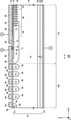
- FIG. 1H is a diagram showing an example of a'a'cross sections in FIG. 1A.
- a cross-sectional view of a region straddling the active region 110 and the outer peripheral region 120 is shown.
- the outer peripheral region 120 of this example has a guard ring structure and a channel stopper structure.
- the guard ring structure may include a plurality of guard ring portions 92.
- the guard ring structure of this example includes five guard ring portions 92.
- Each guard ring portion 92 may be provided on the front surface 21 so as to surround the active region 110 and the pad region 130.
- the guard ring structure may have a function of spreading the depletion layer generated in the active region 110 to the outside of the semiconductor substrate 10. This makes it possible to prevent electric field concentration inside the semiconductor substrate 10. Therefore, the withstand voltage of the semiconductor device 100 can be improved as compared with the case where the guard ring structure is not provided.
- the guard ring portion 92 is a P + type semiconductor region formed by ion implantation in the vicinity of the front surface 21.
- the guard ring portion 92 is electrically connected to the electrode layer 94.
- the electrode layer 94 may be made of the same material as the gate metal layer 50 or the emitter electrode 52.
- the plurality of guard ring portions 92 are electrically insulated from each other by the interlayer insulating film 38.
- the depth of the bottom of the guard ring portion 92 may be the same as the depth of the bottom of the well region 17.
- the depth of the bottom of the guard ring portion 92 may be deeper than the depth of the bottom of the gate trench portion 40 and the dummy trench portion 30.
- the channel stopper structure has a channel stopper region 96 and an electrode layer 94.
- the channel stopper region 96 is electrically connected to the electrode layer 94 through the opening of the interlayer insulating film 38.
- the conductive type of the channel stopper region 96 may be the first conductive type or the second conductive type.
- the conductive type of the channel stopper region 96 of this example is an N + type.
- the channel stopper region 96 has a function of terminating the depletion layer generated in the active region 110 at the outer end portion of the semiconductor substrate 10.
- the well region 17 may extend beyond the well contact region 65 in the arrangement direction and further to the outside.
- the well region 17 of this example may be provided so that the innermost guard ring portion 92 in the outer peripheral region 120 and the outer end portion of the well region 17 are close to each other.
- the base region 14 may be extended to the vicinity of the innermost guard ring portion 92 instead of the well region 17.
- An oxide film 39 may be provided between the contact region 15 and the gate runner 51 above the well region 17.
- the oxide film 39 may be formed in the same process as the dummy insulating film 32 or the gate insulating film 42.
- the oxide film 39 may be formed by a process such as a field oxide film having a thicker film thickness.
- FIG. 2A is an example of a circuit for a clamp withstand voltage test of the semiconductor device 100.
- a gate voltage Vg is applied to the gate terminal of the semiconductor device 100 via a predetermined gate resistance Rg.
- the rated current Ic is switched at a predetermined power supply voltage Vcc.
- the power supply voltage Vcc may be about 60% of the rated voltage.
- the stray inductance Ls is the stray inductance of the circuit to which the semiconductor device 100 is connected. Since the stray inductance Ls tries to maintain the current, a surge voltage is generated when the current is cut off. The stray inductance Ls is increased from a predetermined initial value for each switching, and the semiconductor device 100 is turned off. When the stray inductance Ls is increased, the jump voltage ⁇ V increases. By increasing the stray inductance Ls, the electric field strength inside the semiconductor device 100 increases, and the element is easily destroyed. Here, the result in the test immediately before the element is destroyed is referred to as the clamp energy (that is, the fracture tolerance).
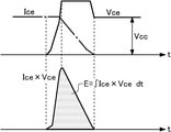
- FIG. 2B is a diagram for explaining the clamping energy of the semiconductor device 100.
- the figure shows the behavior of the collector-emitter current Ice and the collector-emitter voltage Vce at turn-off.
- the graph of this example shows the waveform immediately before the stray inductance Ls in which the element is destroyed by repeating the turn-off while increasing the stray inductance Ls in the clamp withstand voltage test. Due to the turn-off of the semiconductor device 100, the collector-emitter voltage Vce jumps up, and the voltage is held for a certain period of time. The period in which the voltage is constant is the clamping period.
- Clamp energy is the integrated value in the range of current x voltage of 0 or more in the period from the jump of the collector-emitter voltage Vce to the settlement of the power supply voltage Vcc. That is, the clamp energy is represented by an integral value (that is, an energy value) of ⁇ Ice ⁇ Vce dt. The larger the clamp energy, the larger the fracture resistance at turn-off.
- FIG. 3A shows the relationship between the doping concentration of the collector region 22 and the clamping energy.
- the vertical axis represents the clamp energy [mJ]
- the horizontal axis is the integrated value obtained by integrating the doping concentration of the collector region 22 over the depth from the back surface 23 to the PN junction between the collector region 22 and the field stop region 20 (hereinafter,). (Referred to as the integrated value of the doping concentration of the collector region 22) [cm -2 ] is shown.
- the black square indicates the case where the acceleration energy of the proton is 400 keV.
- the white square indicates the case where the acceleration energy of the proton is 300 keV.
- Proton is one of the types of hydrogen ion. Hydrogen donors are formed, for example, by ion-implanting protons into a semiconductor substrate.
- the integrated value of the doping concentration in the collector region 22 is about 1.00E + 14 [cm- 2 ], and the clamp energy becomes the maximum value.
- the proton range of the first peak P1 is 3.13 ⁇ m.
- 1.00E + 14 [cm -2 ] means 1.00 ⁇ 10 14 [cm -2 ].
- the acceleration energy of the proton is 400 keV
- the integrated value of the doping concentration in the collector region 22 is about 1.00E + 13 [cm -2 ], and the clamp energy becomes the maximum value.
- the proton range is 4.52 ⁇ m.
- the injection dose amount may be equal to the integrated value of the doping concentration in the collector region 22.
- the clamp withstand voltage of the active region 110 is made smaller than the clamp withstand voltage of the outer peripheral region 120 by controlling the integrated concentration of the collector region 22 and the peak depth of the field stop region 20. Thereby, the clamping energy of the semiconductor device 100 can be improved.
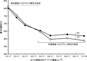
- FIG. 3B shows the relationship between the doping concentration of the collector region 22 and the withstand voltage of the device.
- the vertical axis shows the withstand voltage [V] of the device, and the horizontal axis shows the doping concentration [cm -3 ] of the collector region 22.
- the collector region 22 may comprise a doping concentration distribution with a peak.
- the doping concentration in the collector region 22 may be the peak value of the doping concentration in the collector region 22.
- the field stop region 20 has four peaks will be described.
- Graph G1 shows an activity + edge model when the field stop region 20 has four peaks.
- the activity + edge model is a simulation model that considers both the active region 110 and the outer peripheral region 120.
- Graph G2 shows an activity model when the field stop region 20 has four peaks.
- the activity model is a simulation model in which only the active region 110 is considered without considering the outer peripheral region 120.
- the withstand voltage of the active region 110 is lower than the withstand voltage of the outer peripheral region 120. That is, the withstand voltage of the element is the withstand voltage of the active region 110. In this way, when the withstand voltage of the element is determined in the active region 110, the clamping energy increases.
- the withstand voltage of the active region 110 is higher than the withstand voltage of the outer peripheral region 120. That is, the withstand voltage of the element is the withstand voltage of the outer peripheral region 120. In this way, when the withstand voltage of the element is determined in the outer peripheral region 120, the clamp energy is reduced.
- the doping concentration of the collector region 22 may be 6 ⁇ 10 17 (/ cm 3 ) or less, and may be 5 ⁇ 10 17 (/ cm 3) or less.
- FIG. 4A shows an example of the current-voltage characteristics of the semiconductor device 100 according to the embodiment.
- the vertical axis shows the collector-emitter current Ice [A] and the collector-emitter voltage Vce [V], and the horizontal axis shows the time [s].
- the regions where the electron current density is large are shown by broken lines at time T1 and time T2, respectively.
- the doping concentration of the collector region 22 of this example is set in the range in which the clamp withstand voltage is determined in the active region 110 in FIG. 3B.
- Time T1 is the time when the semiconductor device 100 is turned off and the collector-emitter voltage Vce rises. At time T1, the electron current is concentrated in the region indicated by the broken line in the active region 110. That is, the peak region of the electron current density is formed in a part of the region shown by the broken line of the active region 110.
- Time T2 indicates the time when the collector-emitter voltage Vce rises and is clamped at around 800V.
- the temperature of the avalanche breakdown point rises.
- the lattice vibration becomes intense and electrons are scattered.
- the peak region of the electron current density may move from the active region 110 toward the end of the well region 17 on the outer peripheral region 120 side.
- the withstand voltage of the active region 110 is smaller than the withstand voltage of the outer peripheral region 120
- the peak region of the electron current density formed on the active region 110 side moves to the outer peripheral region 120 side. This temporarily lowers the temperature of the active region 110.
- the power that is, Ice ⁇ Vce
- FIG. 4B shows an example of the current-voltage characteristics of the semiconductor device 500 according to the comparative example.
- the vertical axis shows the collector-emitter current Ice [A] and the collector-emitter voltage Vce [V], and the horizontal axis shows the time [s]. Further, in this example, the peak regions of the electron current densities are shown by broken lines at time T3 and time T4, respectively.
- the doping concentration of the collector region 22 of this example is set in the range in which the withstand voltage is determined in the outer peripheral region 120 in FIG. 3B.
- the integrated concentration of the collector region 22 is set so that the withstand voltage of the outer peripheral region 120 is smaller than the withstand voltage of the active region 110. Due to the turn-off, avalanche breakdown occurs on the outer peripheral region 120 side of the well region 17, and the peak region of the electron current density is formed at the location indicated by the broken line. From time T3 to time T4, the peak region of the electron current density is stagnant at the position indicated by the broken line while the power is high. Therefore, the temperature continues to rise due to current concentration. As described above, in the semiconductor device 500, the element is easily broken and the clamp withstand capacity cannot be improved.
- the carriers tend to concentrate on the contact hole end on the outer peripheral region 120 side, so that the avalanche breakdown is likely to occur.
- the increase in the hole concentration on the back surface 23 side amplifies the avalanche breakdown during clamping.
- the hole injection efficiency of the collector region 22 is lowered by appropriately setting the doping concentration of the collector region 22 and the depth of the first peak P1, and the clamp withstand voltage of the active region 110 is reduced. It is made smaller than the clamp withstand voltage of the outer peripheral region 120. As a result, after the avalanche breakdown occurs in the active region 110, the avalanche breakdown moves to the outer peripheral region 120, so that instantaneous fracture can be suppressed.
- the doping concentration of the collector region 22 and the depth of the first peak P1 may be set so that the clamping energy is maximized. An appropriate range of the doping concentration of the collector region 22 and the depth of the first peak P1 will be described later.
- the voltage is designed to have a withstand voltage higher than the surge voltage (the peak value of the voltage between the collector and emitter that is higher than the power supply voltage at turn-off) that is expected to prevent element destruction when the current is cut off. It is necessary to increase the thickness of the semiconductor substrate 10 in the depth direction and increase the area of the outer peripheral region 120.
- the withstand voltage of the element may be designed to be lower than the surge voltage. In the semiconductor device 100 of this example, the avalanche breakdown is generated in the active region 110 at the time of turn-off, so that the chip cost can be reduced and the element destruction can be prevented.
- the total dose amount of the field stop region 20 and the total dose amount of the collector region 22 may be determined so that the withstand voltage of the active region 110 is smaller than the withstand voltage of the outer peripheral region 120.
- the total dose amount of the field stop region 20 may be 10 times or less the total dose amount of the collector region 22, and may be 5 times or less the total dose amount of the collector region 22.
- FIG. 5A shows an example of the relationship between the integrated concentration of the collector region 22 and the depth of the first peak P1.
- the vertical axis shows the depth y1 [ ⁇ m] of the first peak P1
- the horizontal axis shows the integrated concentration x [cm -2 ] of the collector region 22.
- the next reference line L1 was calculated based on the data of the two points where the acceleration energy of the shallowest proton and the maximum clamp energy were obtained in FIG. 3A.
- Reference line L1: y1 (-6.3067E-01) ln (x) + (2.2590E + 01) That is, the reference line L1 shows the relationship between the integrated concentration of the collector region 22 where the clamping energy is maximized and the depth of the first peak P1 where the clamping energy is maximized.
- the region R1 indicates a region in the range of ⁇ 15% of the reference line L1.
- the region R1 of this example is a region between the line A1 and the line B1.
- the line A1 and the line B1 of this example are represented by the following equations.
- Line A1: y1 (-7.4699E-01) ln (x) + (2.7810E + 01)
- Line B1: y1 (-4.7772E-01) ln (x) + (1.7960E + 01)
- the depth of the first peak P1 and the integrated concentration of the collector region 22 belong to the region R1.
- the hole injection efficiency of the collector region 22 can be suppressed and the clamp pressure resistance of the active region 110 can be made smaller than the clamp pressure resistance of the outer peripheral region 120.
- Integral density of the collector region 22 may be at 1.00E16cm -2 or less, may be 8.00E15cm -2 or less.
- the depth of the first peak P1 may be 0.5 ⁇ m or more and 7.2 ⁇ m or less.
- the avalanche breakdown during clamping can be generated on the active region 110 side. This improves the clamp pressure resistance.
- FIG. 5B shows another example of the relationship between the integrated concentration of the collector region 22 and the depth of the first peak P1.
- the region R1 of this example indicates a region corresponding to ⁇ 10% of the reference line L1.
- the reference line L1 is the same as the reference line L1 in FIG. 5A.
- the line A1 and the line B1 of this example are represented by the following equations.
- Line A1: y1 (-6.9487E-01) ln (x) + (2.5930E + 01)
- Line B1: y1 (-5.2115E-01) ln (x) + (1.9540E + 01)
- the depth of the first peak P1 and the integrated concentration of the collector region 22 may be set so as to belong to the region R1.
- FIG. 5C shows another example of the relationship between the integrated concentration of the collector region 22 and the depth of the first peak P1.
- the region R1 of this example indicates a region corresponding to ⁇ 5% of the reference line L1.
- the reference line L1 is the same as the reference line L1 in FIG. 5A.
- the line A1 and the line B1 of this example are represented by the following equations.
- Line A1: y1 (-6.4710E-01) ln (x) + (2.4190E + 01)
- Line B1: y1 (-5.6458E-01) ln (x) + (2.1130E + 01)
- the depth of the first peak P1 and the integrated concentration of the collector region 22 may be set so as to belong to the region R1 of this example.
- FIG. 6A shows another example of the relationship between the integrated concentration of the collector region 22 and the depth of the first peak P1.
- the reference line L1, the line A, and the line B are the same as each line in FIG. 5A. That is, the region corresponding to ⁇ 15% of the reference line L1 is shown.
- the region R1 of this example indicates a region in which the integrated concentration of the collector region 22 is 3.00E14 cm- 2 or less.
- the depth of the first peak P1 may be 2.0 ⁇ m or more and 7.2 ⁇ m or less.
- the depth of the first peak P1 and the integrated concentration of the collector region 22 may be set so as to belong to the region R1 of this example.
- FIG. 6B shows another example of the relationship between the integrated concentration of the collector region 22 and the depth of the first peak P1.
- the reference line L1, the line A, and the line B are the same as each line in FIG. 5A. That is, the region corresponding to ⁇ 15% of the reference line L1 is shown.
- the region R1 of this example indicates a region in which the integrated concentration of the collector region 22 is 2.00E 14 cm -2 or less.
- the depth of the first peak P1 may be 2.2 ⁇ m or more and 7.2 ⁇ m or less.
- the depth of the first peak P1 and the integrated concentration of the collector region 22 may be set so as to belong to the region R1 of this example.
- FIG. 6C shows another example of the relationship between the integrated concentration of the collector region 22 and the depth of the first peak P1.
- the reference line L1, the line A, and the line B are the same as each line in FIG. 5A. That is, the region corresponding to ⁇ 15% of the reference line L1 is shown.
- the region R1 of this example indicates a region in which the integrated concentration of the collector region 22 is 1.00E14 cm- 2 or less.
- the depth of the first peak P1 may be 2.5 ⁇ m or more and 7.2 ⁇ m or less.
- the depth of the first peak P1 and the integrated concentration of the collector region 22 may be set so as to belong to the region R1 of this example.
- FIG. 6D shows another example of the relationship between the integrated concentration of the collector region 22 and the depth of the first peak P1.
- the reference line L1, the line A, and the line B are the same as each line in FIG. 5A. That is, the region corresponding to ⁇ 15% of the reference line L1 is shown.
- the region R1 of this example indicates a region in which the integrated concentration of the collector region 22 is 5.00E13 cm- 2 or less.
- the depth of the first peak P1 may be 3.0 ⁇ m or more and 7.2 ⁇ m or less.
- the depth of the first peak P1 and the integrated concentration of the collector region 22 may be set so as to belong to the region R1 of this example.
- FIG. 6E shows another example of the relationship between the integrated concentration of the collector region 22 and the depth of the first peak P1.
- the reference line L1, the line A, and the line B are the same as each line in FIG. 5A. That is, the region corresponding to ⁇ 15% of the reference line L1 is shown.
- the region R1 of this example indicates a region in which the integrated concentration of the collector region 22 is 3.00E13 cm- 2 or less.
- the depth of the first peak P1 may be 3.2 ⁇ m or more and 7.2 ⁇ m or less.
- the depth of the first peak P1 and the integrated concentration of the collector region 22 may be set so as to belong to the region R1 of this example.
- FIG. 6F shows another example of the relationship between the integrated concentration of the collector region 22 and the depth of the first peak P1.
- the reference line L1, the line A, and the line B are the same as each line in FIG. 5A. That is, the region corresponding to ⁇ 15% of the reference line L1 is shown.
- the region R1 of this example indicates a region in which the integrated concentration of the collector region 22 is 1.00E13 cm- 2 or less.
- the depth of the first peak P1 may be 3.6 ⁇ m or more and 7.2 ⁇ m or less.
- the depth of the first peak P1 and the integrated concentration of the collector region 22 may be set so as to belong to the region R1 of this example.
- the range of the integrated concentration of the collector region 22 may be limited as shown in FIGS. 6A to 6F.
- the region R1 may be a region in which the integrated concentration of the collector region 22 is 1.00E14cm- 2 or less, may be a region of 5.00E13cm- 2 or less, and may be 3.00E13cm ⁇ . It may be a region of 2 or less, and may be a region of 1.00E 13 cm -2 or less.
- FIG. 7A shows the relationship between the integrated concentration of the collector region 22 and the depth of the second peak P2.
- the vertical axis shows the depth y2 [ ⁇ m] of the second peak P2, and the horizontal axis shows the integrated concentration x [cm -2 ] of the collector region 22.
- the next reference line L2 was calculated based on the data of the two points where the acceleration energy of the shallowest proton and the maximum clamp energy were obtained in FIG. 3A.
- Reference line L2: y2 (-2.4885E + 00) ln (x) + (9.1580E + 01) That is, the reference line L2 shows the relationship between the integrated concentration of the collector region 22 where the clamping energy is maximized and the depth of the second peak P2 where the clamping energy is maximized.
- the region R2 indicates a region in the range of ⁇ 15% of the reference line L2.
- the region R2 of this example is a region between the line A2 and the line B2.
- the line A2 and the line B2 of this example are represented by the following equations.
- Line A2: y2 (-3.1095E + 00) ln (x) + (1.1416E + 02)
- Line B2: y2 (-1.9239E + 00) ln (x) + (7.1030E + 01)
- the depth of the second peak P2 and the integrated concentration of the collector region 22 belong to the region R2.
- the clamping energy is sufficiently high.
- the depth of the second peak P2 may be 3.5 ⁇ m or more and 28 ⁇ m or less.
- FIG. 7B shows another example of the relationship between the integrated concentration of the collector region 22 and the depth of the second peak P2.
- the region R2 of this example indicates a region corresponding to ⁇ 10% of the reference line L2.
- the reference line L2 is the same as the reference line L2 in FIG. 7A.
- the line A2 and the line B2 of this example are represented by the following equations.
- Line A2: y2 (-2.8924E + 00) ln (x) + (1.0629E + 02)
- Line B2: y2 (-2.1020E + 00) ln (x) + (7.7530E + 01)
- the depth of the second peak P2 and the integrated concentration of the collector region 22 may be set so as to belong to the region R2.
- FIG. 7C shows the relationship between the integrated concentration of the collector region 22 and the depth of the second peak P2.
- the region R2 of this example indicates a region corresponding to ⁇ 5% of the reference line L2.
- the reference line L2 is the same as the reference line L2 in FIG. 7A.
- the line A2 and the line B2 of this example are represented by the following equations.
- Line A2: y2 (-2.4885E + 00) ln (x) + (9.1580E + 01)
- Line B2: y2 (-2.2931E + 00) ln (x) + (8.4470E + 01)
- the depth of the second peak P2 and the integrated concentration of the collector region 22 may be set so as to belong to the region R2.
- the range of the integrated concentration of the collector region 22 may be limited as shown in FIGS. 6A to 6F.
- the area R2 can be a region integration density of 1.00E14cm -2 or less of the collector region 22 may be a 5.00E13cm -2 following areas, 3.00E13cm - It may be a region of 2 or less, and may be a region of 1.00E 13 cm -2 or less.
- FIG. 8A is a diagram for explaining the relationship between the stray inductance Ls and the collector current reduction rate dIce / dt.
- the stray inductance Ls is Xc [nH]
- the collector current reduction rate dIce / dt is Yc [A / ⁇ s].
- the stray inductance Ls and the collector current reduction rate dIce / dt are set in a range larger than that of the line C1.
- the range larger than the line C1 refers to a region located above the line C1 in the graph showing the relationship between the stray inductance Ls and the collector current reduction rate dIce / dt.
- the area larger than the line C1 is the area filled with the pattern.
- the stray inductance Ls and the collector current reduction rate dIce / dt may be set in a range larger than that of the line C2.
- the line C2 is represented by the following equation.
- Line C2: Yc 20000Xc -1
- the stray inductance Ls and the collector current reduction rate dIce / dt may be set in a range larger than that of the line C3.
- the line C3 is represented by the following equation.
- Line C3: Yc 50000Xc -1
- the semiconductor device 100 of this example can prevent instantaneous fracture even when the stray inductance Ls and the collector current reduction rate dIce / dt are set in a range larger than any of the wires C1 to C3.
- FIG. 8B is a diagram for explaining the relationship between the specific stray inductance Ls ⁇ A and the current density dJce / dt.
- the specific stray inductance Ls ⁇ A is Xd [nH cm 2 ]
- the current density dJce / dt is Yd [A / (cm 2 ⁇ s)].
- the specific stray inductance Ls ⁇ A is a unique value obtained by multiplying the stray inductance Ls by the area A (cm 2) of the active region 110.
- the current density dJce / dt is a value obtained by dividing the collector current reduction rate dIce / dt by the area A (cm 2) of the active region 110.
- the specific stray inductance Ls ⁇ A and the current density dJce / dt are set in a range larger than the line D1.
- the line D1 is represented by the following equation.
- Line D1: Yd 10000Xd -1
- the specific stray inductance Ls ⁇ A and the current density dJce / dt may be set in a range larger than the line D2.
- the line D2 is represented by the following equation.
- Line D2: Yd 20000Xd -1
- the specific stray inductance Ls ⁇ A and the current density dJce / dt may be set in a range larger than the line D3.
- the line D3 is represented by the following equation.
- Line D3: Yd 50000Xd -1
- the semiconductor device 100 of this example can prevent instantaneous fracture even when the stray inductance Ls and the collector current reduction rate dIce / dt are set in a range larger than any of the wires D1 to D3.
- FIG. 9 is a diagram for explaining the relationship between the specific stray inductance Ls ⁇ A and the specific gate resistance Rg ⁇ A.
- the specific stray inductance Ls ⁇ A is Xe [nH cm 2 ]
- the specific gate resistance Rg ⁇ A is Ye [ ⁇ cm 2 ].
- the specific gate resistance Rg ⁇ A is a unique value obtained by multiplying the gate resistance Rg of the drive circuit of the semiconductor device 100 by the area A (cm 2) of the active region 110.
- the collector current reduction rate dIce / dt changes not only with the stray inductance Ls but also with the gate resistance Rg of the drive circuit of the semiconductor device 100. As the gate resistance Rg decreases, the collector current decrease rate dIce / dt tends to increase.
- the specific stray inductance Ls ⁇ A and the specific gate resistance Rg ⁇ A may be set in a range of the line E1 or less.
- the line E1 is represented by the following equation.
- Line E1: Ye (4.00E-01) Xe
- the specific stray inductance Ls ⁇ A and the specific gate resistance Rg ⁇ A may be set in a range of the line E2 or less.
- the line E2 is expressed by the following equation.
- Line E2: Ye (2.00E-01) Xe
- the specific stray inductance Ls ⁇ A and the specific gate resistance Rg ⁇ A may be set in a range of the line E3 or less.
- the line E3 is represented by the following equation.
- Line E3: Ye (8.00E-02) Xe
- the semiconductor device 100 of this example can prevent instantaneous fracture even when the specific stray inductance Ls ⁇ A and the specific gate resistance Rg ⁇ A are set in the range of any of the wires E1 to E3 or less.
Landscapes
- Metal-Oxide And Bipolar Metal-Oxide Semiconductor Integrated Circuits (AREA)
- Electrodes Of Semiconductors (AREA)
Abstract
半導体基板に設けられた第1導電型のドリフト領域と、ドリフト領域の下方に設けられ、1または複数のピークを有する第1導電型のフィールドストップ領域と、フィールドストップ領域の下方に設けられた第2導電型のコレクタ領域と、を備え、コレクタ領域の積分濃度をx[cm-2]とし、1または複数のピークのうち半導体基板の裏面から最も浅い第1ピークの深さをy1[μm]とし、線A1:y1=(-7.4699E-01)ln(x)+(2.7810E+01)、線B1:y1=(-4.7772E-01)ln(x)+(1.7960E+01)とした場合に、第1ピークの深さおよび積分濃度が、線A1と線B1との間の範囲にある半導体装置を提供する。
Description
本発明は、半導体装置に関する。
従来、フィールドストップ領域を備える半導体装置が知られている(例えば、特許文献1参照)。
特許文献1 特開2015-135954号公報
特許文献1 特開2015-135954号公報
電流遮断時のサージ電圧による素子の破壊を防止することが好ましい。
本発明の第1の態様においては、半導体基板に設けられた第1導電型のドリフト領域と、ドリフト領域の下方に設けられ、1または複数のピークを有する第1導電型のフィールドストップ領域と、フィールドストップ領域の下方に設けられた第2導電型のコレクタ領域と、を備え、コレクタ領域の積分濃度をx[cm-2]とし、1または複数のピークのうち半導体基板の裏面から最も浅い第1ピークの深さをy1[μm]とし、
線A1:y1=(-7.4699E-01)ln(x)+(2.7810E+01)
線B1:y1=(-4.7772E-01)ln(x)+(1.7960E+01)
とした場合に、第1ピークの深さおよび積分濃度が、線A1と線B1との間の範囲にある半導体装置を提供する。
線A1:y1=(-7.4699E-01)ln(x)+(2.7810E+01)
線B1:y1=(-4.7772E-01)ln(x)+(1.7960E+01)
とした場合に、第1ピークの深さおよび積分濃度が、線A1と線B1との間の範囲にある半導体装置を提供する。
コレクタ領域の積分濃度は、8.00E15cm-2以下であってよい。
コレクタ領域の積分濃度は、3.00E14cm-2以下であってよい。
コレクタ領域の積分濃度は、2.00E14cm-2以下であってよい。
コレクタ領域の積分濃度は、1.00E14cm-2以下であってよい。
コレクタ領域の積分濃度は、5.00E13cm-2以下であってよい。
コレクタ領域の積分濃度は、3.00E13cm-2以下であってよい。
コレクタ領域の積分濃度は、1.00E13cm-2以下であってよい。
第1ピークの深さは、0.5μm以上、7.2μm以下であってよい。
第1ピークの深さは、2.0μm以上、7.2μm以下であってよい。
1または複数のピークのうち裏面から2番目に浅い第2ピークの深さをy2[μm]とし、
線A2:y2=(-3.1095E+00)ln(x)+(1.1416E+02)
線B2:y2=(-1.9239E+00)ln(x)+(7.1030E+01)
とした場合に、第2ピークの深さおよび積分濃度が、線A2と線B2との間の範囲にあってよい。
線A2:y2=(-3.1095E+00)ln(x)+(1.1416E+02)
線B2:y2=(-1.9239E+00)ln(x)+(7.1030E+01)
とした場合に、第2ピークの深さおよび積分濃度が、線A2と線B2との間の範囲にあってよい。
第2ピークの深さは、3.5μm以上、28μm以下であってよい。
半導体装置に接続された回路の浮遊インダクタンスLsをXc[nH]、コレクタ電流減少率dIce/dtをYc[A/μs]とし、
線C1:Yc=10000Xc-1
とした場合に、浮遊インダクタンスLsおよびコレクタ電流減少率dIce/dtは、線C1よりも大きい範囲にあってよい。
線C1:Yc=10000Xc-1
とした場合に、浮遊インダクタンスLsおよびコレクタ電流減少率dIce/dtは、線C1よりも大きい範囲にあってよい。
1または複数のピークのドーパントは水素であってよい。
半導体基板に設けられた活性領域と、半導体基板の上面視において、活性領域の外周に設けられた外周領域とを備えてよい。
ドリフト領域の上方に設けられた第2導電型のベース領域と、ベース領域の上方に設けられ、ドリフト領域よりもドーピング濃度の高い第1導電型のエミッタ領域と、ベース領域の上方に設けられ、ベース領域よりもドーピング濃度の高い第2導電型のコンタクト領域と、半導体基板に設けられた複数のゲートトレンチ部とを備えてよい。
フィールドストップ領域とコレクタ領域の境界におけるドーピング濃度は1E16cm-3以下であってよい。
フィールドストップ領域とコレクタ領域の境界におけるドーピング濃度は5E15cm-3以下であってよい。
フィールドストップ領域とコレクタ領域の境界におけるドーピング濃度は2E15cm-3以下であってよい。
フィールドストップ領域とコレクタ領域の境界における水素化学濃度は1E18cm-3以下であってよい。
フィールドストップ領域とコレクタ領域の境界における水素化学濃度は1E17cm-3以下であってよい。
フィールドストップ領域とコレクタ領域の境界における水素化学濃度は1E15cm-3以上であってよい。
フィールドストップ領域とコレクタ領域の境界における水素化学濃度は1E16cm-3以上であってよい。
なお、上記の発明の概要は、本発明の特徴の全てを列挙したものではない。また、これらの特徴群のサブコンビネーションもまた、発明となりうる。
以下、発明の実施の形態を通じて本発明を説明するが、以下の実施形態は請求の範囲にかかる発明を限定するものではない。また、実施形態の中で説明されている特徴の組み合わせの全てが発明の解決手段に必須であるとは限らない。
本明細書においては、半導体基板の深さ方向と平行な方向における一方の側を「上」、他方の側を「下」と称する。基板、層またはその他の部材の2つの主面のうち、一方の面を上面、他方の面を下面と称する。「上」、「下」、「おもて」、「裏」の方向は重力方向、または、半導体装置の実装時における基板等への取り付け方向に限定されない。
本明細書では、X軸、Y軸およびZ軸の直交座標軸を用いて技術的事項を説明する場合がある。直交座標軸は、構成要素の相対位置を特定するに過ぎず、特定の方向を限定するものではない。例えば、Z軸は地面に対する高さ方向を限定して示すものではない。なお、+Z軸方向と-Z軸方向とは互いに逆向きの方向である。正負を記載せず、Z軸方向と記載した場合、+Z軸および-Z軸に平行な方向を意味する。
本明細書では、半導体基板の上面と平行な面をXY面とし、半導体基板の上面および下面に平行な直交軸をX軸およびY軸とする。また、半導体基板の上面および下面と垂直な軸をZ軸とする。半導体基板の深さ方向をZ軸と称する場合がある。なお、本明細書において、Z軸方向に半導体基板を視た場合について平面視と称する。また、本明細書では、X軸およびY軸を含めて、半導体基板の上面および下面に平行な方向を、水平方向と称する場合がある。
各実施例においては、第1導電型をN型、第2導電型をP型とした例を示しているが、第1導電型をP型、第2導電型をN型としてもよい。この場合、各実施例における基板、層、領域等の導電型は、それぞれ逆の極性となる。
本明細書において「同一」または「等しい」のように称した場合、製造ばらつき等に起因する誤差を有する場合も含んでよい。当該誤差は、例えば10%以内である。
本明細書においては、不純物がドーピングされたドーピング領域の導電型をP型またはN型として説明している。本明細書においては、不純物とは、特にN型のドナーまたはP型のアクセプタのいずれかを意味する場合があり、ドーパントと記載する場合がある。本明細書においては、ドーピングとは、半導体基板にドナーまたはアクセプタを導入し、N型の導電型を示す半導体またはP型の導電型を示す半導体とすることを意味する。
本明細書においては、ドーピング濃度とは、熱平衡状態におけるドナーの濃度またはアクセプタの濃度を意味する。本明細書においては、ネット・ドーピング濃度とは、ドナー濃度を正イオンの濃度とし、アクセプタ濃度を負イオンの濃度として、電荷の極性を含めて足し合わせた正味の濃度を意味する。一例として、ドナー濃度をND、アクセプタ濃度をNAとすると、任意の位置における正味のネット・ドーピング濃度はND-NAとなる。
ドナーは、半導体に電子を供給する機能を有している。アクセプタは、半導体から電子を受け取る機能を有している。ドナーおよびアクセプタは、不純物自体には限定されない。例えば、半導体中に存在する空孔(V)、酸素(O)および水素(H)が結合したVOH欠陥は、電子を供給するドナーとして機能する。VOH欠陥を、単に水素ドナーと称する場合がある。
本明細書においてP+型またはN+型と記載した場合、P型またはN型よりもドーピング濃度が高いことを意味し、P-型またはN-型と記載した場合、P型またはN型よりもドーピング濃度が低いことを意味する。また、本明細書においてP++型またはN++型と記載した場合には、P+型またはN+型よりもドーピング濃度が高いことを意味する。
本明細書において化学濃度とは、電気的な活性化の状態によらずに測定される不純物の原子密度を指す。化学濃度は、例えば二次イオン質量分析法(SIMS)により計測できる。上述したネット・ドーピング濃度は、電圧-容量測定法(CV法)により測定できる。また、拡がり抵抗測定法(SR法)により計測されるキャリア濃度を、ネット・ドーピング濃度としてよい。CV法またはSR法により計測されるキャリア濃度は、熱平衡状態における値としてよい。また、N型の領域においては、ドナー濃度がアクセプタ濃度よりも十分大きいので、当該領域におけるキャリア濃度を、ドナー濃度としてもよい。同様に、P型の領域においては、当該領域におけるキャリア濃度を、アクセプタ濃度としてもよい。尚、本発明における各濃度は、室温における値でよい。室温における値は、一例として300K(ケルビン)(約26.9℃)のときの値を用いてよい。
また、ドナー、アクセプタまたはネット・ドーピングの濃度分布がピークを有する場合、当該ピーク値を当該領域におけるドナー、アクセプタまたはネット・ドーピングの濃度としてよい。ドナー、アクセプタまたはネット・ドーピングの濃度がほぼ均一な場合等においては、当該領域におけるドナー、アクセプタまたはネット・ドーピングの濃度の平均値をドナー、アクセプタまたはネット・ドーピングの濃度としてよい。
SR法により計測されるキャリア濃度が、ドナーまたはアクセプタの濃度より低くてもよい。拡がり抵抗を測定する際に電流が流れる範囲において、半導体基板のキャリア移動度が結晶状態の値よりも低い場合がある。キャリア移動度の低下は、格子欠陥等による結晶構造の乱れ(ディスオーダー)により、キャリアが散乱されることで生じる。
CV法またはSR法により計測されるキャリア濃度から算出したドナーまたはアクセプタの濃度は、ドナーまたはアクセプタを示す元素の化学濃度よりも低くてよい。一例として、シリコンの半導体においてドナーとなるリンまたはヒ素のドナー濃度、あるいはアクセプタとなるボロン(ホウ素)のアクセプタ濃度は、これらの化学濃度の99%程度である。一方、シリコンの半導体においてドナーとなる水素のドナー濃度は、水素の化学濃度のたとえば0.1%から10%程度である。
本明細書の単位系は、特に断りがなければSI単位系である。長さの単位をcm等で表示することがあるが、諸計算はメートル(m)に換算してから行ってよい。
本明細書においてドーピング濃度とは、ドナーまたはアクセプタ化したドーパントの濃度を指す。したがって、その単位は、/cm3である。本明細書において、ドナーおよびアクセプタの濃度差(すなわちネットドーピング濃度)をドーピング濃度とする場合がある。この場合、ドーピング濃度はSR法で測定できる。また、ドナーおよびアクセプタの化学濃度をドーピング濃度としてもよい。この場合、ドーピング濃度はSIMS法で測定できる。特に限定していなければ、ドーピング濃度として、上記のいずれを用いてもよい。特に限定していなければ、ドーピング領域におけるドーピング濃度分布のピーク値を、当該ドーピング領域におけるドーピング濃度としてよい。
また、本明細書においてドーズ量とは、イオン注入を行う際に、ウェハに注入される単位面積あたりのイオンの個数をいう。したがって、その単位は、/cm2である。なお、半導体領域のドーズ量は、その半導体領域の深さ方向にわたってドーピング濃度を積分した積分濃度とすることができる。その積分濃度の単位は、/cm2である。したがって、ドーズ量と積分濃度とを同じものとして扱ってよい。積分濃度は、半値幅までの積分値としてもよく、他の半導体領域のスペクトルと重なる場合には、他の半導体領域の影響を除いて導出してよい。
よって、本明細書では、ドーピング濃度の高低をドーズ量の高低として読み替えることができる。即ち、一の領域のドーピング濃度が他の領域のドーピング濃度よりも高い場合、当該一の領域のドーズ量が他の領域のドーズ量よりも高いものと理解することができる。
図1Aは、半導体装置100の上面図の一例である。半導体装置100は、活性領域110と、外周領域120と、パッド領域130とを備える。半導体装置100は、トランジスタ部70およびダイオード部80を備える半導体チップである。半導体装置100は、温度センス部76を備え、IPM(Intelligent Power Module)等のモジュールに搭載されてよい。
トランジスタ部70は、IGBT(Insulated Gate Bipolar Transistor)等のトランジスタを含む。ダイオード部80は、還流ダイオード(FWD:Free Wheel Diode)等のダイオードを含む。本例の半導体装置100は、トランジスタ部70およびダイオード部80を同一のチップに有する逆導通IGBT(RC-IGBT:Reverse Conducting IGBT)である。本例では、トランジスタ部70のトランジスタは、IGBTである。
半導体基板10は、シリコン基板であってよく、炭化シリコン基板であってよく、窒化ガリウム等の窒化物半導体基板等であってもよい。本例の半導体基板10は、シリコン基板である。半導体基板10は、活性領域110および外周領域120を有する。
トランジスタ部70およびダイオード部80は、XY平面内において交互に周期的に配列されてよい。本例の半導体装置100は、複数のトランジスタ部70および複数のダイオード部80をそれぞれ備える。本例のトランジスタ部70およびダイオード部80は、Y軸方向に延伸するトレンチ部を有する。但し、トランジスタ部70およびダイオード部80は、X軸方向に延伸するトレンチ部を有していてもよい。
温度センス部76は、活性領域110の上方に設けられる。温度センス部76は、単結晶または多結晶のシリコンで形成されてよい。半導体装置100の温度が変化すると、温度センス部76に流れる電流の順方向電圧が変化する。順方向電圧の変化に基づいて、半導体装置100の温度を検出することができる。
活性領域110は、トランジスタ部70およびダイオード部80を有する。活性領域110は、半導体装置100をオン状態に制御した場合に、半導体基板10のおもて面と裏面との間で主電流が流れる領域である。即ち、半導体基板10のおもて面から裏面、または裏面からおもて面に、半導体基板10の内部を深さ方向に電流が流れる領域である。本明細書では、トランジスタ部70およびダイオード部80をそれぞれ素子部または素子領域と称する。
なお、上面視において、2つの素子部に挟まれた領域も活性領域110とする。本例では、素子部に挟まれてゲートランナー51が設けられている領域も活性領域110に含めている。
ゲートランナー51は、パッド領域130のゲートパッド131から供給されるゲート電位をトランジスタ部70のゲート導電部に供給してよい。ゲートランナー51は、上面視において、活性領域110の外周に沿って設けられている。ゲートランナー51は、上面視において、トランジスタ部70およびダイオード部80の間の領域にも設けられてよい。
外周領域120は、上面視において、活性領域110とパッド領域130を囲むように半導体基板10の端部周辺に設けられる。半導体基板10の外周端との間の領域である。外周領域120は、上面視において、活性領域110を囲んで設けられる。外周領域120は、エッジ終端構造部を有してよい。エッジ終端構造部は、半導体基板10のおもて面側の電界集中を緩和する。例えば、エッジ終端構造部は、ガードリング、フィールドプレート、リサーフおよびこれらを組み合わせた構造を有する。
パッド領域130は、ゲートパッド131、センスIGBT132、センスエミッタパッド133、アノードパッド134およびカソードパッド135を有する。本例では、カソードパッド135、アノードパッド134、ゲートパッド131、センスIGBT132およびセンスエミッタパッド133がこの順でX軸方向に並べて設けられる。各パッドは、金(Au)、銀(Ag)、銅(Cu)またはアルミニウム(Al)等を含む電極パッドであってよい。
ゲートパッド131は、ゲートランナー51を介してトランジスタ部70のゲート導電部と電気的に接続される。ゲートパッド131は、ゲート電位に設定されている。
センスIGBT132は、トランジスタ部70に流れる主電流を検出するためのIGBTである。センスIGBT132には、トランジスタ部70に流れる主電流に比例した電流が流れる。センスIGBT132に流れるセンス電流を、半導体装置100の外部に設けられた制御回路に取り込むことにより、トランジスタ部70の主電流を検出することができる。本例のセンスエミッタパッド133は、センスIGBT132のエミッタと同じ電位を有する。センス電流は、センスIGBT132を経てセンスエミッタパッド133から上述の制御回路に取り込まれてよい。制御回路はセンス電流に基づいて主電流を検知して、トランジスタ部70に過電流が流れている場合にトランジスタ部70に流れる電流を遮断してよい。
アノードパッド134は、温度センス部76と電気的に接続され、温度センス部76のアノード電位に設定される。同様に、カソードパッド135は、温度センス部76と電気的に接続され、温度センス部76のカソード電位に設定される。アノードパッド134およびカソードパッド135を用いて、温度センス部76のアノード‐カソード間の電位差を検知することができる。
図1Bは、図1Aの領域Aに対応する半導体装置100の上面図の一例である。即ち、活性領域110の端部の拡大図を示している。
トランジスタ部70は、半導体基板10の裏面側に設けられたコレクタ領域22を半導体基板10のおもて面に投影した領域である。コレクタ領域22は、第2導電型を有する。本例のコレクタ領域22は、一例としてP+型である。トランジスタ部70は、トランジスタ部70とダイオード部80の境界に位置する境界部90を含む。
ダイオード部80は、半導体基板10の裏面側に設けられたカソード領域82を半導体基板10のおもて面に投影した領域である。カソード領域82は、第1導電型を有する。本例のカソード領域82は、一例としてN+型である。
本例の半導体装置100は、半導体基板10のおもて面において、ゲートトレンチ部40と、ダミートレンチ部30と、エミッタ領域12と、ベース領域14と、コンタクト領域15と、ウェル領域17とを備える。また、本例の半導体装置100は、半導体基板10のおもて面の上方に設けられたエミッタ電極52およびゲート金属層50を備える。
エミッタ電極52は、ゲートトレンチ部40、ダミートレンチ部30、エミッタ領域12、ベース領域14、コンタクト領域15およびウェル領域17の上方に設けられている。また、ゲート金属層50は、ウェル領域17およびゲートランナー51の上方に設けられている。本例のエミッタ電極52は、トランジスタ部70のエミッタ電位に設定されている。
ゲート金属層50は、トランジスタ部70のゲート導電部と電気的に接続され、トランジスタ部70にゲート電圧を供給する。ゲート金属層50は、ゲートパッド131と電気的に接続される。ゲート金属層50は、上面視で、活性領域110の外周に沿って設けられる。ゲート金属層50は、上面視で、トランジスタ部70およびダイオード部80の間にも設けられてよい。
ゲートランナー51は、ゲート金属層50とゲートトレンチ部40内のゲート導電部とを接続する。ゲートランナー51は、ダミートレンチ部30内のダミー導電部とは接続されない。例えば、ゲートランナー51は、不純物がドープされたポリシリコン等で形成される。
エミッタ電極52およびゲート金属層50は、金属を含む材料で形成される。例えば、エミッタ電極52の少なくとも一部の領域は、アルミニウム、アルミニウム‐シリコン合金、またはアルミニウム‐シリコン‐銅合金で形成されてよい。エミッタ電極52は、アルミニウム等で形成された領域の下層にチタンやチタン化合物等で形成されたバリアメタルを有してよい。エミッタ電極52およびゲート金属層50は、互いに分離して設けられる。
エミッタ電極52およびゲート金属層50は、層間絶縁膜38を挟んで、半導体基板10の上方に設けられる。層間絶縁膜38は、図1Bでは省略されている。層間絶縁膜38には、コンタクトホール54、コンタクトホール55およびコンタクトホール56が貫通して設けられている。
コンタクトホール55は、ゲート金属層50とゲートランナー51とを接続する。コンタクトホール55の内部には、タングステン等で形成されたプラグが形成されてもよい。コンタクトホール55は、ゲートランナー51に沿って設けられてよい。
コンタクトホール56は、エミッタ電極52とダミートレンチ部30内のダミー導電部とを接続する。コンタクトホール56の内部には、タングステン等で形成されたプラグが形成されてもよい。
接続部25は、エミッタ電極52とコンタクトホール56の内部のプラグとを電気的に接続する。接続部25は、不純物がドープされたポリシリコン等の導電性材料を有する。本例の接続部25は、N型の不純物がドープされたポリシリコンである。接続部25は、上面視において、コンタクトホール56よりも大きな範囲を覆う。接続部25は、酸化膜等の絶縁膜等を介して、半導体基板10のおもて面の上方に設けられる。
ゲートトレンチ部40は、予め定められた配列方向(本例ではX軸方向)に沿って予め定められた間隔で配列される。本例のゲートトレンチ部40は、半導体基板10のおもて面に平行であって配列方向と垂直な延伸方向(本例ではY軸方向)に沿って延伸する2つの延伸部分41と、2つの延伸部分41を接続する接続部分43を有してよい。
接続部分43は、少なくとも一部が曲線状に形成されることが好ましい。ゲートトレンチ部40の2つの延伸部分41の端部を接続することで、延伸部分41の端部における電界集中を緩和できる。ゲートトレンチ部40の接続部分43において、ゲートランナー51がゲート導電部と接続されてよい。
ダミートレンチ部30は、エミッタ電極52と電気的に接続されたトレンチ部である。ダミートレンチ部30は、ゲートトレンチ部40と同様に、予め定められた配列方向(本例ではX軸方向)に沿って予め定められた間隔で配列される。本例のダミートレンチ部30は、ゲートトレンチ部40と同様に、半導体基板10のおもて面においてU字形状を有してよい。即ち、ダミートレンチ部30は、延伸方向に沿って延伸する2つの延伸部分31と、2つの延伸部分31を接続する接続部分33を有してよい。
ウェル領域17は、後述するドリフト領域18よりも半導体基板10のおもて面側に設けられた第2導電型の領域である。ウェル領域17は、半導体装置100のエッジ側に設けられるウェル領域の一例である。ウェル領域17は、一例としてP+型である。ウェル領域17は、ゲート金属層50が設けられる側の活性領域110の端部から、予め定められた範囲で形成される。ウェル領域17の拡散深さは、ゲートトレンチ部40およびダミートレンチ部30の深さよりも深くてよい。ゲートトレンチ部40およびダミートレンチ部30の、ゲート金属層50側の一部の領域は、ウェル領域17に形成される。ゲートトレンチ部40およびダミートレンチ部30の延伸方向の端の底は、ウェル領域17に覆われてよい。
コンタクトホール54は、トランジスタ部70において、エミッタ領域12およびコンタクト領域15の各領域の上方に形成される。また、コンタクトホール54は、ダイオード部80において、ベース領域14の上方に設けられる。コンタクトホール54は、境界部90において、コンタクト領域15の上方に設けられる。いずれのコンタクトホール54も、延伸方向の両端に設けられたウェル領域17の上方には設けられていない。このように、層間絶縁膜38には、1または複数のコンタクトホール54が形成されている。1または複数のコンタクトホール54は、延伸方向に延伸して設けられてよい。
境界部90は、トランジスタ部70に設けられ、ダイオード部80と隣接する領域である。境界部90は、コンタクト領域15を有する。本例の境界部90は、エミッタ領域12を有さない。本例の境界部90は、配列方向における両端がダミートレンチ部30となるように配置されている。
メサ部71、メサ部91およびメサ部81は、半導体基板10のおもて面と平行な面内において、トレンチ部に隣接して設けられたメサ部である。メサ部とは、隣り合う2つのトレンチ部に挟まれた半導体基板10の部分であって、半導体基板10のおもて面から、各トレンチ部の最も深い底部の深さまでの部分であってよい。各トレンチ部の延伸部分を1つのトレンチ部としてよい。即ち、2つの延伸部分に挟まれる領域をメサ部としてよい。
メサ部71は、トランジスタ部70において、ダミートレンチ部30またはゲートトレンチ部40の少なくとも1つに隣接して設けられる。メサ部71は、半導体基板10のおもて面において、ウェル領域17と、エミッタ領域12と、ベース領域14と、コンタクト領域15とを有する。メサ部71では、エミッタ領域12およびコンタクト領域15が延伸方向において交互に設けられている。
メサ部91は、境界部90に設けられている。メサ部91は、半導体基板10のおもて面において、ベース領域14と、コンタクト領域15と、ウェル領域17とを有する。本例のメサ部91は、配列方向の両端がダミートレンチ部30と接しているが、少なくとも一方がゲートトレンチ部40と接していてもよい。本例では、1つのメサ部91が設けられているが、複数のメサ部91が設けられてもよい。
メサ部81は、ダイオード部80において、隣り合うダミートレンチ部30に挟まれた領域に設けられる。メサ部81は、半導体基板10のおもて面において、ベース領域14およびウェル領域17を有する。
ベース領域14は、トランジスタ部70およびダイオード部80において、半導体基板10のおもて面側に設けられた第2導電型の領域である。ベース領域14は、一例としてP-型である。ベース領域14は、半導体基板10のおもて面において、メサ部71およびメサ部91の延伸方向における両端部に設けられてよい。なお、図1Bは、当該ベース領域14の延伸方向の一方の端部のみを示している。
エミッタ領域12は、ドリフト領域18よりもドーピング濃度の高い第1導電型の領域である。本例のエミッタ領域12は、一例としてN+型である。エミッタ領域12のドーパントの一例はヒ素(As)である。エミッタ領域12は、メサ部71のおもて面において、ゲートトレンチ部40と接して設けられる。エミッタ領域12は、メサ部71を挟んだ2本のトレンチ部の一方から他方まで、配列方向に延伸して設けられてよい。エミッタ領域12は、コンタクトホール54の下方にも設けられている。
また、エミッタ領域12は、ダミートレンチ部30と接してもよいし、接しなくてもよい。本例のエミッタ領域12は、ダミートレンチ部30と接している。エミッタ領域12は、境界部90のメサ部91には設けられなくてよい。
コンタクト領域15は、ベース領域14よりもドーピング濃度の高い第2導電型の領域である。本例のコンタクト領域15は、一例としてP+型である。本例のコンタクト領域15は、メサ部71およびメサ部91のおもて面に設けられている。コンタクト領域15は、メサ部71またはメサ部91を挟んだ2本のトレンチ部の一方から他方まで、配列方向に設けられてよい。コンタクト領域15は、ゲートトレンチ部40と接してもよいし、接しなくてもよい。また、コンタクト領域15は、ダミートレンチ部30と接してもよいし、接しなくてもよい。本例においては、コンタクト領域15が、ダミートレンチ部30およびゲートトレンチ部40と接する。コンタクト領域15は、コンタクトホール54の下方にも設けられている。なお、コンタクト領域15は、メサ部81にも設けられてよい。
図1Cは、図1Bにおけるb-b'断面の一例を示す図である。b-b'断面は、トランジスタ部70において、エミッタ領域12を通過するXZ面である。本例の半導体装置100は、b-b'断面において、半導体基板10、層間絶縁膜38、エミッタ電極52およびコレクタ電極24を有する。エミッタ電極52は、半導体基板10および層間絶縁膜38の上方に形成される。
ドリフト領域18は、半導体基板10に設けられた第1導電型の領域である。本例のドリフト領域18は、一例としてN-型である。ドリフト領域18は、半導体基板10において他のドーピング領域が形成されずに残存した領域であってよい。即ち、ドリフト領域18のドーピング濃度は半導体基板10のドーピング濃度であってよい。
フィールドストップ領域20は、ドリフト領域18の下方に設けられた第1導電型の領域である。本例のフィールドストップ領域20は、一例としてN型である。フィールドストップ領域20のドーピング濃度は、ドリフト領域18のドーピング濃度よりも高い。フィールドストップ領域20は、ベース領域14の下面側から広がる空乏層が、第2導電型のコレクタ領域22および第1導電型のカソード領域82に到達することを防ぐ。
フィールドストップ領域20は、1または複数のピークを有してよい。本例のフィールドストップ領域20は、第1ピークP1~第4ピークP4の4つのピークを有する。1または複数のピークのドーパントは水素であってよい。
第1ピークP1~第4ピークP4は、この順で裏面23から順に設けられる。即ち、第1ピークP1が最も裏面23に近いピークである。第1ピークP1のドーピング濃度は、他のピークのドーピング濃度よりも高くてよい。これにより、電圧印加時の空乏層をゆっくりと確実に止めることができる。
コレクタ領域22は、トランジスタ部70において、フィールドストップ領域20の下方に設けられる。カソード領域82は、ダイオード部80において、フィールドストップ領域20の下方に設けられる。コレクタ領域22とカソード領域82との境界は、トランジスタ部70とダイオード部80との境界である。
コレクタ電極24は、半導体基板10の裏面23に形成される。コレクタ電極24は、金属等の導電材料で形成される。
ベース領域14は、メサ部71、メサ部91およびメサ部81において、ベース領域14の上方に設けられる第2導電型の領域である。ベース領域14は、ゲートトレンチ部40に接して設けられる。ベース領域14は、ダミートレンチ部30に接して設けられてよい。
エミッタ領域12は、メサ部71において、ベース領域14とおもて面21との間に設けられる。エミッタ領域12は、ゲートトレンチ部40と接して設けられる。エミッタ領域12は、ダミートレンチ部30と接してもよいし、接しなくてもよい。なお、エミッタ領域12は、メサ部91に設けられなくてよい。
コンタクト領域15は、メサ部91において、ベース領域14の上方に設けられる。コンタクト領域15は、メサ部91において、ゲートトレンチ部40に接して設けられる。他の断面において、コンタクト領域15は、メサ部71のおもて面21に設けられてよい。
蓄積領域16は、ドリフト領域18よりも半導体基板10のおもて面21側に設けられる第1導電型の領域である。本例の蓄積領域16は、一例としてN+型である。蓄積領域16は、トランジスタ部70およびダイオード部80に設けられる。本例の蓄積領域16は、境界部90にも設けられている。
また、蓄積領域16は、ゲートトレンチ部40に接して設けられる。蓄積領域16は、ダミートレンチ部30に接してもよいし、接しなくてもよい。蓄積領域16のドーピング濃度は、ドリフト領域18のドーピング濃度よりも高い。蓄積領域16を設けることで、キャリア注入促進効果(IE効果)を高めて、トランジスタ部70のオン電圧を低減できる。
1つ以上のゲートトレンチ部40および1つ以上のダミートレンチ部30は、おもて面21に設けられる。各トレンチ部は、おもて面21からドリフト領域18まで設けられる。エミッタ領域12、ベース領域14、コンタクト領域15および蓄積領域16の少なくともいずれかが設けられる領域においては、各トレンチ部はこれらの領域も貫通して、ドリフト領域18に到達する。トレンチ部がドーピング領域を貫通するとは、ドーピング領域を形成してからトレンチ部を形成する順序で製造したものに限定されない。トレンチ部を形成した後に、トレンチ部の間にドーピング領域を形成したものも、トレンチ部がドーピング領域を貫通しているものに含まれる。
ゲートトレンチ部40は、おもて面21に形成されたゲートトレンチ、ゲート絶縁膜42およびゲート導電部44を有する。ゲート絶縁膜42は、ゲートトレンチの内壁を覆って形成される。ゲート絶縁膜42は、ゲートトレンチの内壁の半導体を酸化または窒化して形成してよい。ゲート導電部44は、ゲートトレンチの内部においてゲート絶縁膜42よりも内側に形成される。ゲート絶縁膜42は、ゲート導電部44と半導体基板10とを絶縁する。ゲート導電部44は、ポリシリコン等の導電材料で形成される。ゲートトレンチ部40は、おもて面21において層間絶縁膜38により覆われる。
ゲート導電部44は、半導体基板10の深さ方向において、ゲート絶縁膜42を挟んでメサ部71側で隣接するベース領域14と対向する領域を含む。ゲート導電部44に予め定められた電圧が印加されると、ベース領域14のうちゲートトレンチに接する界面の表層に、電子の反転層によるチャネルが形成される。
ダミートレンチ部30は、ゲートトレンチ部40と同一の構造を有してよい。ダミートレンチ部30は、おもて面21側に形成されたダミートレンチ、ダミー絶縁膜32およびダミー導電部34を有する。ダミー絶縁膜32は、ダミートレンチの内壁を覆って形成される。ダミー導電部34は、ダミートレンチの内部に形成され、且つ、ダミー絶縁膜32よりも内側に形成される。ダミー絶縁膜32は、ダミー導電部34と半導体基板10とを絶縁する。ダミートレンチ部30は、おもて面21において層間絶縁膜38により覆われる。
層間絶縁膜38は、おもて面21に設けられている。層間絶縁膜38の上方には、エミッタ電極52が設けられている。層間絶縁膜38には、エミッタ電極52と半導体基板10とを電気的に接続するための1又は複数のコンタクトホール54が設けられている。コンタクトホール55およびコンタクトホール56も同様に、層間絶縁膜38を貫通して設けられてよい。
図1Dは、図1Bのc-c'線の位置における、深さ方向のドーピング濃度分布の一例を示す図である。c-c'線は、トランジスタ部70において、エミッタ領域12からコレクタ領域22まで通過する。図1Dの縦軸は、対数軸である。なお、本例ではトランジスタ部70におけるフィールドストップ領域20のドーピング濃度分布を説明するが、ダイオード部80におけるフィールドストップ領域20も同様のドーピング濃度分布を有してよい。
本例のドリフト領域18のドーピング濃度は、バルク・ドナー濃度Dbである。本例の半導体基板10は、第1導電型(N型)のバルク・ドナーが全体に分布している。バルク・ドナーは、半導体基板10の元となるインゴットの製造時に、インゴット内に略一様に含まれたドーパントによるドナーである。本例のバルク・ドナーは、水素以外の元素である。バルク・ドナーのドーパントは、例えばリン、アンチモン、ヒ素、セレン、硫黄であるが、これに限定されない。本例のバルク・ドナーは、リンである。バルク・ドナーは、P型の領域にも含まれている。半導体基板10は、半導体のインゴットから切り出したウェハであってよく、ウェハを個片化したチップであってもよい。半導体のインゴットは、チョクラルスキー法(CZ法)、磁場印加型チョクラルスキー法(MCZ法)、フロートゾーン法(FZ法)のいずれかで製造されよい。本例におけるインゴットは、MCZ法で製造されている。バルク・ドナー濃度Dbは、半導体基板10の全体に分布しているドナーの化学濃度を用いてよく、当該化学濃度の90%から100%の間の値であってもよい。
本例では、フィールドストップ領域20におけるドーピング濃度分布が、深さ方向において異なる位置に4つの濃度ピークP1、P2、P3、P4を有する場合について説明する。但し、濃度ピークの数はこれに限定されない。本例において濃度ピークは、ドナー濃度のピークである。複数の濃度ピークは、水素またはリン等の不純物を、フィールドストップ領域20の複数の深さ位置に注入することで形成できる。一例として、P1の位置をリンとし、P2~P4をドナーとしての水素を用いてよい。本例ではP1~P4の全てがドナーとしての水素である。フィールドストップ領域20は、濃度ピークと対応する位置に、水素またはリン等の不純物の濃度ピークを有していてよい。不純物の濃度ピークは、不純物の化学濃度分布におけるピークである。複数の濃度ピークを設けることで、空乏層がコレクタ領域22に達することを、より抑制できる。
図1Eは、図1Cのフィールドストップ領域20およびコレクタ領域22におけるドーピング濃度分布の拡大図である。図1Eの縦軸は、対数軸である。図1Eにおいて、複数の濃度ピークP1、P2、P3、P4のドーピング濃度のピーク値は、それぞれd1、d2、d3、d4である。また、コレクタ領域22とフィールドストップ領域20との間のpn接合の深さをJ1とする。
複数の濃度ピークは、半導体基板10の裏面23に最も近い最浅ピークを含む。本例では、濃度ピークP1が最浅ピークに相当する。本例の濃度ピークP1は、コレクタ領域22に最も近い濃度ピークである。ダイオード部80のフィールドストップ領域20においては、濃度ピークP1は、カソード領域82に最も近い濃度ピークである。カソード領域82は、濃度ピークとは異なる不純物を注入することで形成されてよい。例えばカソード領域82はリン等の不純物濃度ピークを有し、フィールドストップ領域20は水素等の不純物濃度ピークを有する。
複数の濃度ピークは、最浅ピーク(濃度ピークP1)よりも、裏面23から離れた位置に配置された高濃度ピークを含む。高濃度ピークは、最浅ピークに最も近い濃度ピークP2であってよく、他の濃度ピークであってもよい。図1Eの例では、濃度ピークP1に最も近い濃度ピークP2が高濃度ピークに相当する。
複数の濃度ピークは、高濃度ピークよりも裏面23から離れた位置に配置され、ドーピング濃度のピーク値が高濃度ピークのピーク値の1/5以下である低濃度ピークを含む。低濃度ピークは、複数の濃度ピークのうち、裏面23から最も離れて配置された最深ピーク(本例では濃度ピークP4)であってよい。低濃度ピークは、最深ピーク以外の濃度ピークであってもよい。つまり低濃度ピークは、高濃度ピークと最深ピークとの間の濃度ピークであってもよい。
また、低濃度ピークが2つ以上設けられていてもよい。低濃度ピークは、深さ方向に隣り合って配置されることが好ましい。複数の濃度ピークのうち、裏面23から最も遠くに配置された2つ以上の濃度ピークが、低濃度ピークであってよい。図1Eの例では、最深ピークである濃度ピークP4と、裏面23に向かって最深ピークの次に裏面23から離れた位置に設けられた濃度ピークP3と、P3の次に裏面23に近い濃度ピークP2とが、低濃度ピークである。最も裏面23に近い濃度ピーク以外の濃度ピークを、低濃度ピークとしてもよい。図1Eの例においては、濃度ピークP3のドーピング濃度のピーク値d3と、濃度ピークP4のドーピング濃度のピーク値d4のいずれもが、濃度ピークP1のドーピング濃度のピーク値d1の1/5以下である。低濃度ピークP2~P4の濃度ピークd2~d4が、濃度ピークP1のピーク値d1の1/10以下であってよい。なお、本例ではP3のピーク値d3がP4のピーク値d4よりも低くなっている。P3のピーク値d3は、P4のピーク値d4より高くてもよい。すなわち、P2からP4のピーク値は、おもて面21に向かって低下してよい。
直列に接続された2つの半導体装置100が同時にオンする短絡状態等においては、半導体装置100のエミッタ/コレクタ間に高電圧が印加される場合がある。この場合、フィールドストップ領域20における最深ピーク(本例では濃度ピークP4)の近傍に、電界が集中しやすくなる。このため、濃度ピークP3および濃度ピークP4等のように、最深ピークの近傍におけるドーピング濃度を高くすると、電界の集中が促進されてしまう。電界が集中すると、半導体装置100のターンオフ時等においてゲート電圧が振動しやすくなる。
本例の濃度ピークは、高濃度ピーク(濃度ピークP1)よりも深い位置に、ドーピング濃度が十分小さい低濃度ピークを設けている。このため、フィールドストップ領域20の深い位置における電界集中を緩和できる。上述したように、低濃度ピークは一以上であってよく、複数設けられていてもよい。これにより、比較的に低濃度のフィールドストップ領域20を、ドリフト領域18側に長く形成できる。図1Eの例では、フィールドストップ領域20は3つの低濃度ピークを有しているが、他の例では、フィールドストップ領域20は4つ以上の低濃度ピークを有していてもよい。また、最深ピークは、半導体基板10のおもて面21側に設けられていてもよい。フィールドストップ領域20のドリフト領域18側を低濃度領域としつつ、低濃度領域を深さ方向に長く形成することで、電界集中を緩和しつつ、フィールドストップ機能を維持しやすくなる。
低濃度ピークのドーピング濃度のピーク値は、高濃度ピークのドーピング濃度のピーク値の1/5以下であってよく、1/10以下であってよく、1/20以下であってもよい。低濃度ピークのドーピング濃度を低くすることで、電界集中をより緩和できる。
また、低濃度ピークのドーピング濃度のピーク値は、バルク・ドナー濃度Dbよりも高い。低濃度ピークのドーピング濃度のピーク値は、半導体基板10のバルク・ドナー濃度Dbの50倍以下であってもよい。ドリフト領域18のドーピング濃度を、バルク・ドナー濃度Dbとして用いてよい。低濃度ピークのドーピング濃度のピーク値は、バルク・ドナー濃度Dbの20倍以下であってよく、10倍以下であってよく、8倍以下であってよく、5倍以下であってよく、3倍以下であってよく、2倍以下であってもよい。
また、低濃度ピークのピーク間におけるドーピング濃度の極小値は、バルク・ドナー濃度Dbよりも高くてよく、バルク・ドナー濃度Dbの5倍以下であってよく、3倍以下であってよく、2倍以下であってよい。隣り合う低濃度ピークのどちらかのピーク濃度に対する、ピーク間の極小値の比は、0.8以下であってよく、0.5以下であってよく、0.2以下であってよく、0.1以上であってよく、0.2以上であってよく、0.5以上であってよい。
濃度ピークP1、P2、P3、P4の深さ方向における位置を、それぞれZ1、Z2、Z3、Z4とする。濃度ピークP4と、濃度ピークP2との深さ方向における距離はZ4-Z2である。また、濃度ピークP1と、濃度ピークP2との深さ方向における距離はZ2-Z1である。距離Z4-Z2は、距離Z2-Z1より大きくてよい。また、濃度ピークP3と、濃度ピークP4との距離はZ4-Z3である。濃度ピークP3と、濃度ピークP2との距離はZ3-Z2である。距離Z4-Z3は、距離Z3-Z2より大きくてよい。また、距離Z4-Z3は、距離Z2-Z1より大きくてよい。
また、濃度ピークP4のドーピング濃度のピーク値が、高濃度ピークのドーピング濃度のピーク値の1/5以下であってよく、1/10以下であってよく、1/20以下であってもよい。濃度ピークP4のドーピング濃度のピーク値は、バルク・ドナー濃度Dbよりも高い。濃度ピークP4と、濃度ピークP3のドーピング濃度のピーク値の平均値が、バルク・ドナー濃度Dbの50倍以下であってよく、20倍以下であってよく、10倍以下であってよく、8倍以下であってよく、5倍以下であってよく、3倍以下であってよく、2倍以下であってもよい。最も深い2つの濃度ピークのドーピング濃度の平均値を小さくすることで、ドリフト領域18の近傍のフィールドストップ領域20における電界集中を緩和できる。
本例において、コレクタ領域22とフィールドストップ領域20の間のpn接合J1において、ドナー濃度またはアクセプタ濃度は、1E16/cm3以下であってよく、5E15/cm3以下であってよく、2E15/cm3以下であってよい。なお、Eは10のべき乗を意味し、例えば1E16/cm3は1×1016/cm3を意味する。
図1Fは、第1の濃度ピークおよびコレクタ領域22における、深さ方向のネット・ドーピング濃度及び水素化学濃度の分布の一例を示す図である。実線がネット・ドーピング濃度の分布の一例を表しており、破線が水素化学濃度の分布の一例を表している。図1Fの縦軸は対数軸である。ここで、図1Fに斜線で示した領域が、本例におけるコレクタ領域22の積分濃度である。すなわち、本明細書において、コレクタ領域22の積分濃度とは、コレクタ領域22のネット・ドーピング濃度を、裏面からフィールドストップ領域20とのpn接合位置J1まで半導体基板10の深さ方向に積分した濃度を意味する。また、コレクタ領域22とフィールドストップ領域20の間のpn接合J1における水素化学濃度Dhは、1E18/cm3以下であってよく、1E17/cm3以下であってよく、1E16/cm3以上であってよく、1E15/cm3以上であってよい。
図1Gは、図1Aの領域Bに対応する半導体装置100の上面図の一例である。本例では、活性領域110の端部の拡大図を示している。領域Bは、活性領域110のトランジスタ部70およびゲートランナー51を含む領域である。本例の半導体装置100は、ダミートレンチ領域60およびウェルコンタクト領域65を備える。
ダミートレンチ領域60は、トレンチ部としてダミートレンチ部30のみを有する領域である。ダミートレンチ領域60は、配列方向において、外周領域120に最も近いゲートトレンチ部40と外周領域120との間に設けられる。ダミートレンチ領域60は、配列方向において所定の間隔だけ離間して配置された複数のダミートレンチ部30を有する。
ウェルコンタクト領域65は、ウェル領域17の一部に設けられ、コレクタ領域22から注入されたホールをエミッタ電極52へと引き抜く。ウェルコンタクト領域65は、コンタクト領域15を有する。ウェルコンタクト領域65のコンタクト領域15上には、コンタクトホール54が設けられる。コンタクト領域15は、複数のコンタクトホール54を通じてエミッタ電極52と電気的に接続される。なお、半導体装置100は、ウェルコンタクト領域65を備えなくてもよい。
メサ部61には、ベース領域14、コンタクト領域15およびウェル領域17が設けられる。コンタクト領域15は、メサ部61において、配列方向において隣接する一方のダミートレンチ部30から、他方のダミートレンチ部30まで設けられる。本例のメサ部61は、コンタクト領域15を有するので、コンタクト領域15を有さない場合と比較して、ホールを引き抜きやすくなる。これにより、ウェル領域17の端部におけるアバランシェ電流の集中による半導体装置100の破壊を防止する。
エミッタ電極52は、ダミートレンチ領域60およびウェルコンタクト領域65の上方にも設けられる。エミッタ電極52は、コンタクトホール54を介して、ダミートレンチ領域60、ウェルコンタクト領域65およびトランジスタ部70のそれぞれにおいて、半導体基板10のおもて面21と電気的に接続されている。
ウェル領域17は、上面視において、活性領域110の外周側に設けられる。ウェル領域17の内側端部を破線で示している。
蓄積領域16は、トランジスタ部70からダミートレンチ領域60に延伸して設けられている。本例の蓄積領域16は、トランジスタ部70からダミートレンチ領域60の途中のメサ部61まで延伸して設けられている。蓄積領域16をトランジスタ部70からダミートレンチ領域60に延伸して設けることにより、蓄積領域16の形成用のマスクにずれが生じた場合であっても、トランジスタ部70に形成される蓄積領域16への影響が小さくなる。これにより、ゲート閾値電圧(Vth)のばらつき、および、飽和電流のばらつきを抑制できる。蓄積領域16の外側端部を破線で示している。
図1Hは、図1Aにおけるa-a'断面の一例を示す図である。本例では、活性領域110および外周領域120にまたがる領域の断面図を示している。本例の外周領域120は、ガードリング構造およびチャネルストッパ構造を有する。
ガードリング構造は、複数のガードリング部92を含んでよい。本例のガードリング構造は5つのガードリング部92を含む。各ガードリング部92は、おもて面21において活性領域110およびパッド領域130を囲むように設けられてよい。
ガードリング構造は、活性領域110において発生した空乏層を半導体基板10の外側へ広げる機能を有してよい。これにより、半導体基板10内部における電界集中を防ぐことができる。それゆえ、ガードリング構造を設けない場合と比較して、半導体装置100の耐圧を向上させることができる。
ガードリング部92は、おもて面21近傍にイオン注入により形成されたP+型の半導体領域である。ガードリング部92は、電極層94と電気的に接続される。電極層94は、ゲート金属層50またはエミッタ電極52と同じ材料であってよい。
複数のガードリング部92は、層間絶縁膜38によって互いに電気的に絶縁される。ガードリング部92の底部の深さは、ウェル領域17の底部と同じ深さであってよい。ガードリング部92の底部の深さは、ゲートトレンチ部40およびダミートレンチ部30の底部の深さより深くてよい。
チャネルストッパ構造は、チャネルストッパ領域96および電極層94を有する。チャネルストッパ領域96は、層間絶縁膜38の開口を通じて電極層94と電気的に接続する。チャネルストッパ領域96の導電型は、第1導電型であっても、第2導電型であってもよい。本例のチャネルストッパ領域96の導電型は、N+型である。チャネルストッパ領域96は、活性領域110において発生した空乏層を半導体基板10の外側端部において終端させる機能を有する。
ウェル領域17は、配列方向においてウェルコンタクト領域65を超えて、さらに外側まで延伸してよい。本例のウェル領域17は、外周領域120における最も内側のガードリング部92とウェル領域17の外側端部との距離が近接するように設けられてよい。なお、本例の変形例として、ウェル領域17に代えて、ベース領域14を最も内側のガードリング部92の近傍まで拡張して設けてもよい。なお、ウェル領域17の上方において、コンタクト領域15とゲートランナー51との間に酸化膜39が設けられてよい。酸化膜39は、ダミー絶縁膜32またはゲート絶縁膜42と同一の工程で形成されてもよい。あるいは、酸化膜39は、より膜厚の厚いフィールド酸化膜等の工程で形成されてもよい。
図2Aは、半導体装置100のクランプ耐量試験用の回路の一例である。半導体装置100のゲート端子には予め定められたゲート抵抗Rgを介して、ゲート電圧Vgが与えられている。クランプ耐量試験では、定格電流Icを、予め定められた電源電圧Vccでスイッチングさせる。電源電圧Vccは、定格電圧の6割程度であってよい。
浮遊インダクタンスLsは、半導体装置100が接続される回路の浮遊インダクタンスである。浮遊インダクタンスLsが電流を維持しようとするため、電流遮断時にサージ電圧が発生する。浮遊インダクタンスLsを予め定められた初期値からスイッチング1回ごとに高くして、半導体装置100をターンオフさせる。浮遊インダクタンスLsを増加させると、跳ね上がり電圧ΔVが増加する。浮遊インダクタンスLsを増加させることにより、半導体装置100の内部の電界強度が増加して、素子が破壊されやすくなる。ここで、素子が破壊に至る1つ前の試験における結果をクランプエネルギ(即ち、破壊耐量)とする。
図2Bは、半導体装置100のクランプエネルギを説明するための図である。同図は、ターンオフ時のコレクタ-エミッタ電流Iceおよびコレクタ-エミッタ間電圧Vceの挙動を示している。本例のグラフは、クランプ耐量試験において、浮遊インダクタンスLsを増加させながらターンオフを繰り返し、素子が破壊した浮遊インダクタンスLsの1つ前の波形を示している。半導体装置100のターンオフによって、コレクタ-エミッタ間電圧Vceが跳ね上がり、一定期間、電圧が保持されている。電圧が一定の期間がクランプ期間である。
クランプエネルギは、コレクタ-エミッタ間電圧Vceの跳ね上がりから電源電圧Vccに落ち着くまでの期間で、電流×電圧が0以上の範囲における積分値である。即ち、クランプエネルギは、∫Ice×Vce dtの積分値(即ち、エネルギ値)で示される。クランプエネルギが大きいほどターンオフ時の破壊耐量が大きいことを示す。
図3Aは、コレクタ領域22のドーピング濃度とクランプエネルギとの関係を示す。縦軸はクランプエネルギ[mJ]を示し、横軸はコレクタ領域22のドーピング濃度を、裏面23から、コレクタ領域22とフィールドストップ領域20とのPN接合までの深さにわたって積分した積分値(以下、コレクタ領域22のドーピング濃度の積分値と称す)[cm-2]を示す。黒色の四角は、プロトンの加速エネルギが400keVの場合を示す。白色の四角は、プロトンの加速エネルギが300keVの場合を示す。プロトンは水素イオンの種類の一つである。水素ドナーは、たとえばプロトンを半導体基板にイオン注入することにより形成される。
プロトンの加速エネルギが小さいほどプロトンの総ドーズ量が小さくなり、クランプエネルギが上昇しやすくなる。また、プロトンの総ドーズ量が小さいと、アバランシェ降伏時に裏面23から注入される正孔濃度が増加して、活性領域110側でアバランシェ降伏が発生しやすくなる。このように、活性領域110のクランプ耐圧が外周領域120のクランプ耐圧よりも低下すると、後述の通り、外周領域120における瞬時破壊を防止しやすくなる。瞬時破壊とは、例えばターンオフ時に、電流が遮断される前に素子が破壊することである。
例えば、プロトンの加速エネルギが300keVの場合、コレクタ領域22のドーピング濃度の積分値がおよそ1.00E+14[cm-2]でクランプエネルギが最大値となる。この場合、例えば、第1ピークP1のプロトン飛程が3.13μmとなる。なお、1.00E+14[cm-2]とは、1.00×10¹⁴[cm-2]を示している。
また、プロトンの加速エネルギが400keVの場合、コレクタ領域22のドーピング濃度の積分値がおよそ1.00E+13[cm-2]でクランプエネルギが最大値となる。この場合、例えばプロトン飛程が4.52μmとなる。
なお、コレクタ領域22のドーピング濃度の積分値は、裏面ボロンの注入ドーズ量とおよそ等しいので、注入ドーズ量=コレクタ領域22のドーピング濃度の積分値としてよい。
本例の半導体装置100は、コレクタ領域22の積分濃度とフィールドストップ領域20のピーク深さを制御することにより、活性領域110のクランプ耐圧を外周領域120のクランプ耐圧よりも小さくする。これにより、半導体装置100のクランプエネルギを向上することができる。
図3Bは、コレクタ領域22のドーピング濃度と素子の耐圧との関係を示す。縦軸は素子の耐圧[V]を示し、横軸はコレクタ領域22のドーピング濃度[cm-3]を示す。コレクタ領域22はピークを有するドーピング濃度分布を備えてよい。この場合、コレクタ領域22のドーピング濃度は、コレクタ領域22のドーピング濃度のピーク値であってよい。本例では、フィールドストップ領域20が4つのピークを有する場合について説明する。
グラフG1は、フィールドストップ領域20が4つのピークを有する場合の活性+エッジモデルを示す。活性+エッジモデルは、活性領域110と外周領域120の両方を考慮したシミュレーションモデルである。グラフG2は、フィールドストップ領域20が4つのピークを有する場合の活性モデルを示す。活性モデルは、外周領域120を考慮せず、活性領域110のみを考慮したシミュレーションモデルである。
コレクタ領域22のドーピング濃度を小さくすることにより、活性領域110の耐圧が外周領域120の耐圧よりも低下する。即ち、素子の耐圧は活性領域110の耐圧となる。このように、素子の耐圧が活性領域110で決定されるようになると、クランプエネルギが増加する。
一方、コレクタ領域22のドーピング濃度を大きくすることにより、活性領域110の耐圧が外周領域120の耐圧よりも増加する。即ち、素子の耐圧は外周領域120の耐圧となる。このように、素子の耐圧が外周領域120で決定されるようになると、クランプエネルギが低下する。以上により、クランプエネルギを高くするために、コレクタ領域22のドーピング濃度は6×10¹⁷(/cm3)以下であってよく、5×1017(/cm3)以下であってよい。
図4Aは、実施例に係る半導体装置100の電流電圧特性の一例を示す。縦軸はコレクタ-エミッタ電流Ice[A]およびコレクタ-エミッタ間電圧Vce[V]を示し、横軸は時刻[s]を示す。また、半導体装置100の断面図では、時刻T1および時刻T2において、電子電流密度が大きな領域をそれぞれ破線で示している。本例のコレクタ領域22のドーピング濃度は、図3Bにおいて、活性領域110でクランプ耐圧が決定される範囲に設定されている。
時刻T1は、半導体装置100がターンオフしてコレクタ-エミッタ間電圧Vceが上昇したタイミングの時刻である。時刻T1では、活性領域110の破線で示す領域に電子電流が集中している。即ち、活性領域110の破線で示す領域の一部で、電子電流密度のピーク領域が形成されている。
時刻T2は、コレクタ-エミッタ間電圧Vceが上昇して、800V前後でクランプされている時刻を示す。時刻T2において、アバランシェ降伏箇所の温度が上昇する。温度上昇により格子振動が激しくなり、電子が散乱する。電子の散乱により電流が流れにくくなると、電子電流密度のピーク領域が、活性領域110からウェル領域17の外周領域120側の端部に向かって移動する場合がある。
このように、活性領域110の耐圧が外周領域120の耐圧よりも小さい場合、活性領域110側に形成された電子電流密度のピーク領域が、外周領域120側に移動する。これにより一時的に活性領域110の温度が低下する。また、アバランシェ降伏による電子電流密度のピーク領域が外周領域120側に移動したときには、パワー(即ち、Ice×Vce)が低下している。したがって、半導体装置100の温度上昇を緩和して、瞬時破壊を防止することができる。
図4Bは、比較例に係る半導体装置500の電流電圧特性の一例を示す。縦軸はコレクタ-エミッタ電流Ice[A]およびコレクタ-エミッタ間電圧Vce[V]を示し、横軸は時刻[s]を示す。また、本例では、時刻T3および時刻T4において、電子電流密度のピーク領域をそれぞれ破線で示している。本例のコレクタ領域22のドーピング濃度は、図3Bにおいて、外周領域120で耐圧が決定される範囲に設定されている。
半導体装置500は、外周領域120の耐圧が活性領域110の耐圧よりも小さくなるように、コレクタ領域22の積分濃度が設定されている。ターンオフにより、ウェル領域17の外周領域120側でアバランシェ降伏が発生し、電子電流密度のピーク領域が破線で示す箇所に形成される。時刻T3から時刻T4において、パワーが高い状態で、電子電流密度のピーク領域は破線で示した位置に停滞している。このため、電流集中により温度が上昇し続ける。このように、半導体装置500では、素子が破壊されやすくなり、クランプ耐量を向上することができない。
外周領域120では、コレクタ領域22の正孔注入効率に応じたアバランシェ降伏の増幅に加えて、外周領域120側のコンタクトホール端にキャリアが集中しやすいことにより、アバランシェ降伏が発生しやすくなる。裏面23側の正孔濃度の上昇は、クランプ時のアバランシェ降伏を増幅させる。
本例の半導体装置100は、コレクタ領域22のドーピング濃度と第1ピークP1の深さを適切に設定することにより、コレクタ領域22の正孔注入効率を低下させて、活性領域110のクランプ耐圧を外周領域120のクランプ耐圧よりも小さくする。これにより、活性領域110でアバランシェ降伏が発生した後に、外周領域120へとアバランシェ降伏が移動するので、瞬時破壊を抑制できる。コレクタ領域22のドーピング濃度と第1ピークP1の深さは、クランプエネルギが最大となるように設定されてよい。コレクタ領域22のドーピング濃度と第1ピークP1の深さの適切な範囲については後述する。
なお、電流遮断時の素子破壊を防止するために想定されるサージ電圧(ターンオフ時に、コレクタ・エミッタ間電圧が電源電圧よりも増加した電圧のピーク値のこと)以上の耐圧を持つように設計すると、半導体基板10の深さ方向の厚みを厚くしたり、外周領域120の面積を大きくしたりする必要がある。チップコストを低減するために、素子の耐圧をサージ電圧以下に設計する場合がある。本例の半導体装置100は、ターンオフ時に活性領域110でアバランシェ降伏を発生させることにより、チップコストを低減しつつ、素子破壊を防止することができる。
また、活性領域110の耐圧が外周領域120の耐圧よりも小さくなるように、フィールドストップ領域20の総ドーズ量と、コレクタ領域22の総ドーズ量を決定してよい。例えば、フィールドストップ領域20の総ドーズ量は、コレクタ領域22の総ドーズ量の10倍以下であってよく、コレクタ領域22の総ドーズ量の5倍以下であってもよい。
図5Aは、コレクタ領域22の積分濃度と第1ピークP1の深さとの関係の例を示す。縦軸は第1ピークP1の深さy1[μm]を示し、横軸はコレクタ領域22の積分濃度x[cm-2]を示す。
ここで、図3Aで得られたプロトン最浅の加速エネルギと、クランプエネルギが最大となる2点のデータに基づいて、次の基準線L1を算出した。
基準線L1:y1=(-6.0367E-01)ln(x)+(2.2590E+01)
即ち、基準線L1は、クランプエネルギが最大となるコレクタ領域22の積分濃度と、クランプエネルギが最大となる第1ピークP1の深さとの関係を示している。
基準線L1:y1=(-6.0367E-01)ln(x)+(2.2590E+01)
即ち、基準線L1は、クランプエネルギが最大となるコレクタ領域22の積分濃度と、クランプエネルギが最大となる第1ピークP1の深さとの関係を示している。
領域R1は、基準線L1の±15%の範囲の領域を示す。本例の領域R1は、線A1と線B1との間の領域である。本例の線A1および線B1は、次式で示される。
線A1:y1=(-7.4699E-01)ln(x)+(2.7810E+01)
線B1:y1=(-4.7772E-01)ln(x)+(1.7960E+01)
この場合、第1ピークP1の深さおよびコレクタ領域22の積分濃度が、領域R1に属する。領域R1であれば、コレクタ領域22の正孔注入効率を抑制して、活性領域110のクランプ耐圧を外周領域120のクランプ耐圧よりも小さくすることができる。コレクタ領域22の積分濃度は、1.00E16cm-2以下であってよく、8.00E15cm-2以下であってもよい。第1ピークP1の深さは、0.5μm以上、7.2μm以下であってよい。
線A1:y1=(-7.4699E-01)ln(x)+(2.7810E+01)
線B1:y1=(-4.7772E-01)ln(x)+(1.7960E+01)
この場合、第1ピークP1の深さおよびコレクタ領域22の積分濃度が、領域R1に属する。領域R1であれば、コレクタ領域22の正孔注入効率を抑制して、活性領域110のクランプ耐圧を外周領域120のクランプ耐圧よりも小さくすることができる。コレクタ領域22の積分濃度は、1.00E16cm-2以下であってよく、8.00E15cm-2以下であってもよい。第1ピークP1の深さは、0.5μm以上、7.2μm以下であってよい。
本例の半導体装置100は、コレクタ領域22の積分濃度と、第1ピークP1の深さを領域R1に設定することにより、クランピング時のアバランシェ降伏を活性領域110側で発生させることができる。これにより、クランプ耐圧が向上する。
図5Bは、コレクタ領域22の積分濃度と第1ピークP1の深さとの関係の他の例を示す。本例の領域R1は、基準線L1の±10%に該当する領域を示している。
基準線L1は、図5Aの基準線L1と同一である。本例の線A1および線B1は、次式で示される。
線A1:y1=(-6.9487E-01)ln(x)+(2.5930E+01)
線B1:y1=(-5.2115E-01)ln(x)+(1.9540E+01)
この場合も同様に、第1ピークP1の深さおよびコレクタ領域22の積分濃度が、領域R1に属するように設定されてよい。
線A1:y1=(-6.9487E-01)ln(x)+(2.5930E+01)
線B1:y1=(-5.2115E-01)ln(x)+(1.9540E+01)
この場合も同様に、第1ピークP1の深さおよびコレクタ領域22の積分濃度が、領域R1に属するように設定されてよい。
図5Cは、コレクタ領域22の積分濃度と第1ピークP1の深さとの関係の他の例を示す。本例の領域R1は、基準線L1の±5%に該当する領域を示している。
基準線L1は、図5Aの基準線L1と同一である。本例の線A1および線B1は、次式で示される。
線A1:y1=(-6.4710E-01)ln(x)+(2.4190E+01)
線B1:y1=(-5.6458E-01)ln(x)+(2.1130E+01)
この場合も同様に、第1ピークP1の深さおよびコレクタ領域22の積分濃度が、本例の領域R1に属するように設定されてよい。
線A1:y1=(-6.4710E-01)ln(x)+(2.4190E+01)
線B1:y1=(-5.6458E-01)ln(x)+(2.1130E+01)
この場合も同様に、第1ピークP1の深さおよびコレクタ領域22の積分濃度が、本例の領域R1に属するように設定されてよい。
図6Aは、コレクタ領域22の積分濃度と第1ピークP1の深さとの関係の他の例を示す。基準線L1、線Aおよび線Bは、図5Aの各線と同一である。即ち、基準線L1の±15%に該当する領域を示している。但し、本例の領域R1は、コレクタ領域22の積分濃度が3.00E14cm-2以下である領域を示している。第1ピークP1の深さは、2.0μm以上、7.2μm以下であってよい。第1ピークP1の深さおよびコレクタ領域22の積分濃度が、本例の領域R1に属するように設定されてよい。
図6Bは、コレクタ領域22の積分濃度と第1ピークP1の深さとの関係の他の例を示す。基準線L1、線Aおよび線Bは、図5Aの各線と同一である。即ち、基準線L1の±15%に該当する領域を示している。但し、本例の領域R1は、コレクタ領域22の積分濃度が2.00E14cm-2以下である領域を示している。第1ピークP1の深さは、2.2μm以上、7.2μm以下であってよい。第1ピークP1の深さおよびコレクタ領域22の積分濃度が、本例の領域R1に属するように設定されてよい。
図6Cは、コレクタ領域22の積分濃度と第1ピークP1の深さとの関係の他の例を示す。基準線L1、線Aおよび線Bは、図5Aの各線と同一である。即ち、基準線L1の±15%に該当する領域を示している。但し、本例の領域R1は、コレクタ領域22の積分濃度が1.00E14cm-2以下である領域を示している。第1ピークP1の深さは、2.5μm以上、7.2μm以下であってよい。第1ピークP1の深さおよびコレクタ領域22の積分濃度が、本例の領域R1に属するように設定されてよい。
図6Dは、コレクタ領域22の積分濃度と第1ピークP1の深さとの関係の他の例を示す。基準線L1、線Aおよび線Bは、図5Aの各線と同一である。即ち、基準線L1の±15%に該当する領域を示している。但し、本例の領域R1は、コレクタ領域22の積分濃度が5.00E13cm-2以下である領域を示している。第1ピークP1の深さは、3.0μm以上、7.2μm以下であってよい。第1ピークP1の深さおよびコレクタ領域22の積分濃度が、本例の領域R1に属するように設定されてよい。
図6Eは、コレクタ領域22の積分濃度と第1ピークP1の深さとの関係の他の例を示す。基準線L1、線Aおよび線Bは、図5Aの各線と同一である。即ち、基準線L1の±15%に該当する領域を示している。但し、本例の領域R1は、コレクタ領域22の積分濃度が3.00E13cm-2以下である領域を示している。第1ピークP1の深さは、3.2μm以上、7.2μm以下であってよい。第1ピークP1の深さおよびコレクタ領域22の積分濃度が、本例の領域R1に属するように設定されてよい。
図6Fは、コレクタ領域22の積分濃度と第1ピークP1の深さとの関係の他の例を示す。基準線L1、線Aおよび線Bは、図5Aの各線と同一である。即ち、基準線L1の±15%に該当する領域を示している。但し、本例の領域R1は、コレクタ領域22の積分濃度が1.00E13cm-2以下である領域を示している。第1ピークP1の深さは、3.6μm以上、7.2μm以下であってよい。第1ピークP1の深さおよびコレクタ領域22の積分濃度が、本例の領域R1に属するように設定されてよい。
なお、図5Bおよび図5Cについても、図6A~図6Fのように、コレクタ領域22の積分濃度の範囲を制限してもよい。例えば、図5Bおよび図5Cにおいて、領域R1は、コレクタ領域22の積分濃度が1.00E14cm-2以下の領域であってよく、5.00E13cm-2以下の領域であってよく、3.00E13cm-2以下の領域であってよく、1.00E13cm-2以下の領域であってもよい。
図7Aは、コレクタ領域22の積分濃度と第2ピークP2の深さとの関係を示す。縦軸は第2ピークP2の深さy2[μm]を示し、横軸はコレクタ領域22の積分濃度x[cm-2]を示す。
ここで、図3Aで得られたプロトン最浅の加速エネルギと、クランプエネルギが最大となる2点のデータに基づいて、次の基準線L2を算出した。
基準線L2:y2=(-2.4885E+00)ln(x)+(9.1580E+01)
即ち、基準線L2は、クランプエネルギが最大となるコレクタ領域22の積分濃度と、クランプエネルギが最大となる第2ピークP2の深さとの関係を示している。
基準線L2:y2=(-2.4885E+00)ln(x)+(9.1580E+01)
即ち、基準線L2は、クランプエネルギが最大となるコレクタ領域22の積分濃度と、クランプエネルギが最大となる第2ピークP2の深さとの関係を示している。
領域R2は、基準線L2の±15%の範囲の領域を示す。本例の領域R2は、線A2と線B2との間の領域である。本例の線A2および線B2は、次式で示される。
線A2:y2=(-3.1095E+00)ln(x)+(1.1416E+02)
線B2:y2=(-1.9239E+00)ln(x)+(7.1030E+01)
この場合、第2ピークP2の深さおよびコレクタ領域22の積分濃度が、領域R2に属する。領域R2であれば、クランプエネルギが十分高くなる。第2ピークP2の深さは、3.5μm以上、28μm以下であってよい。
線A2:y2=(-3.1095E+00)ln(x)+(1.1416E+02)
線B2:y2=(-1.9239E+00)ln(x)+(7.1030E+01)
この場合、第2ピークP2の深さおよびコレクタ領域22の積分濃度が、領域R2に属する。領域R2であれば、クランプエネルギが十分高くなる。第2ピークP2の深さは、3.5μm以上、28μm以下であってよい。
図7Bは、コレクタ領域22の積分濃度と第2ピークP2の深さとの関係の他の例を示す。本例の領域R2は、基準線L2の±10%に該当する領域を示している。
基準線L2は、図7Aの基準線L2と同一である。本例の線A2および線B2は、次式で示される。
線A2:y2=(-2.8924E+00)ln(x)+(1.0629E+02)
線B2:y2=(-2.1020E+00)ln(x)+(7.7530E+01)
この場合も同様に、第2ピークP2の深さおよびコレクタ領域22の積分濃度が、領域R2に属するように設定されてよい。
線A2:y2=(-2.8924E+00)ln(x)+(1.0629E+02)
線B2:y2=(-2.1020E+00)ln(x)+(7.7530E+01)
この場合も同様に、第2ピークP2の深さおよびコレクタ領域22の積分濃度が、領域R2に属するように設定されてよい。
図7Cは、コレクタ領域22の積分濃度と第2ピークP2の深さとの関係を示す。本例の領域R2は、基準線L2の±5%に該当する領域を示している。
基準線L2は、図7Aの基準線L2と同一である。本例の線A2および線B2は、次式で示される。
線A2:y2=(-2.4885E+00)ln(x)+(9.1580E+01)
線B2:y2=(-2.2931E+00)ln(x)+(8.4470E+01)
この場合も同様に、第2ピークP2の深さおよびコレクタ領域22の積分濃度が、領域R2に属するように設定されてよい。
線A2:y2=(-2.4885E+00)ln(x)+(9.1580E+01)
線B2:y2=(-2.2931E+00)ln(x)+(8.4470E+01)
この場合も同様に、第2ピークP2の深さおよびコレクタ領域22の積分濃度が、領域R2に属するように設定されてよい。
なお、図7A~図7Cについても、図6A~図6Fのように、コレクタ領域22の積分濃度の範囲を制限してもよい。例えば、図7A~図7Cにおいて、領域R2は、コレクタ領域22の積分濃度が1.00E14cm-2以下の領域であってよく、5.00E13cm-2以下の領域であってよく、3.00E13cm-2以下の領域であってよく、1.00E13cm-2以下の領域であってもよい。
図8Aは、浮遊インダクタンスLsとコレクタ電流減少率dIce/dtとの関係を説明するための図である。浮遊インダクタンスLsをXc[nH]とし、コレクタ電流減少率dIce/dtをYc[A/μs]としている。線C1は次式で示される。
線C1:Yc=10000Xc-1
浮遊インダクタンスLsおよびコレクタ電流減少率dIce/dtは、線C1よりも大きい範囲に設定される。線C1よりも大きい範囲とは、浮遊インダクタンスLsとコレクタ電流減少率dIce/dtとの関係を示したグラフにおいて、線C1の上側に位置する領域を指す。線C1よりも大きい範囲は、パターンで塗りつぶされた領域である。
線C1:Yc=10000Xc-1
浮遊インダクタンスLsおよびコレクタ電流減少率dIce/dtは、線C1よりも大きい範囲に設定される。線C1よりも大きい範囲とは、浮遊インダクタンスLsとコレクタ電流減少率dIce/dtとの関係を示したグラフにおいて、線C1の上側に位置する領域を指す。線C1よりも大きい範囲は、パターンで塗りつぶされた領域である。
浮遊インダクタンスLsおよびコレクタ電流減少率dIce/dtは、線C2よりも大きい範囲に設定されてよい。線C2は次式で示される。
線C2:Yc=20000Xc-1
線C2:Yc=20000Xc-1
浮遊インダクタンスLsおよびコレクタ電流減少率dIce/dtは、線C3よりも大きい範囲に設定されてよい。線C3は次式で示される。
線C3:Yc=50000Xc-1
線C3:Yc=50000Xc-1
ここで、浮遊インダクタンスLsが大きくなるほど、電流を維持しやすくなり、電流遮断時にサージ電圧が大きくなる。また、コレクタ電流減少率dIce/dtが大きいほど、電流遮断時にサージ電圧が大きくなる。そのため、線C1~線C3のいずれかよりも大きい範囲に浮遊インダクタンスLsおよびコレクタ電流減少率dIce/dtを設定した場合、サージ電圧が跳ね上がりやすくなる。本例の半導体装置100は、線C1~線C3のいずれかよりも大きい範囲に浮遊インダクタンスLsおよびコレクタ電流減少率dIce/dtを設定した場合であっても、瞬時破壊を防止できる。
図8Bは、比浮遊インダクタンスLs・Aと電流密度dJce/dtとの関係を説明するための図である。比浮遊インダクタンスLs・AをXd[nH cm2]とし、電流密度dJce/dtをYd[A/(cm2μs)]としている。
比浮遊インダクタンスLs・Aは、浮遊インダクタンスLsに活性領域110の面積A(cm2)を掛けた固有の値である。電流密度dJce/dtは、コレクタ電流減少率dIce/dtを活性領域110の面積A(cm2)で割った値である。
比浮遊インダクタンスLs・Aおよび電流密度dJce/dtは、線D1よりも大きい範囲に設定される。線D1は次式で示される。
線D1:Yd=10000Xd-1
線D1:Yd=10000Xd-1
比浮遊インダクタンスLs・Aおよび電流密度dJce/dtは、線D2よりも大きい範囲に設定されてよい。線D2は次式で示される。
線D2:Yd=20000Xd-1
線D2:Yd=20000Xd-1
比浮遊インダクタンスLs・Aおよび電流密度dJce/dtは、線D3よりも大きい範囲に設定されてよい。線D3は次式で示される。
線D3:Yd=50000Xd-1
線D3:Yd=50000Xd-1
ここで、比浮遊インダクタンスLs・Aまたは電流密度dJce/dtが大きいほど、電流遮断時にサージ電圧が大きくなる。そのため、線D1~線D3のいずれかよりも大きい範囲に比浮遊インダクタンスLs・Aまたは電流密度dJce/dtを設定した場合、サージ電圧が跳ね上がりやすくなる。本例の半導体装置100は、線D1~線D3のいずれかよりも大きい範囲に浮遊インダクタンスLsおよびコレクタ電流減少率dIce/dtを設定した場合であっても、瞬時破壊を防止できる。
図9は、比浮遊インダクタンスLs・Aと比ゲート抵抗Rg・Aとの関係を説明するための図である。比浮遊インダクタンスLs・AをXe[nH cm2]とし、比ゲート抵抗Rg・AをYe[Ωcm2]としている。比ゲート抵抗Rg・Aは、半導体装置100の駆動回路のゲート抵抗Rgに、活性領域110の面積A(cm2)を掛けた固有の値である。
コレクタ電流減少率dIce/dtは、浮遊インダクタンスLsの他に、半導体装置100の駆動回路のゲート抵抗Rgによっても変化する。ゲート抵抗Rgが減少すると、コレクタ電流減少率dIce/dtは増加する傾向にある。
比浮遊インダクタンスLs・Aおよび比ゲート抵抗Rg・Aは、線E1以下となる範囲に設定されてよい。線E1は次式で示される。
線E1:Ye=(4.000E-01)Xe
線E1:Ye=(4.000E-01)Xe
比浮遊インダクタンスLs・Aおよび比ゲート抵抗Rg・Aは、線E2以下となる範囲に設定されてよい。線E2は次式で示される。
線E2:Ye=(2.000E-01)Xe
線E2:Ye=(2.000E-01)Xe
比浮遊インダクタンスLs・Aおよび比ゲート抵抗Rg・Aは、線E3以下となる範囲に設定されてよい。線E3は次式で示される。
線E3:Ye=(8.000E-02)Xe
線E3:Ye=(8.000E-02)Xe
ここで、比ゲート抵抗Rg・Aが小さいほど、電流遮断時にサージ電圧が大きくなる。そのため、線E1~線E3のいずれか以下となる範囲に、比浮遊インダクタンスLs・Aおよび比ゲート抵抗Rg・Aを設定した場合、サージ電圧が跳ね上がりやすくなる。本例の半導体装置100は、線E1~線E3のいずれか以下となる範囲に、比浮遊インダクタンスLs・Aおよび比ゲート抵抗Rg・Aを設定した場合であっても、瞬時破壊を防止できる。
以上、本発明を実施の形態を用いて説明したが、本発明の技術的範囲は上記実施の形態に記載の範囲には限定されない。上記実施の形態に、多様な変更または改良を加えることが可能であることが当業者に明らかである。その様な変更または改良を加えた形態も本発明の技術的範囲に含まれ得ることが、請求の範囲の記載から明らかである。
請求の範囲、明細書、および図面中において示した装置、システム、プログラム、および方法における動作、手順、ステップ、および段階等の各処理の実行順序は、特段「より前に」、「先立って」等と明示しておらず、また、前の処理の出力を後の処理で用いるのでない限り、任意の順序で実現しうることに留意すべきである。請求の範囲、明細書、および図面中の動作フローに関して、便宜上「まず、」、「次に、」等を用いて説明したとしても、この順で実施することが必須であることを意味するものではない。
10・・・半導体基板、12・・・エミッタ領域、14・・・ベース領域、15・・・コンタクト領域、16・・・蓄積領域、17・・・ウェル領域、18・・・ドリフト領域、20・・・フィールドストップ領域、21・・・おもて面、22・・・コレクタ領域、23・・・裏面、24・・・コレクタ電極、25・・・接続部、30・・・ダミートレンチ部、31・・・延伸部分、32・・・ダミー絶縁膜、33・・・接続部分、34・・・ダミー導電部、38・・・層間絶縁膜、39・・・酸化膜、40・・・ゲートトレンチ部、41・・・延伸部分、42・・・ゲート絶縁膜、43・・・接続部分、44・・・ゲート導電部、50・・・ゲート金属層、51・・・ゲートランナー、52・・・エミッタ電極、54・・・コンタクトホール、55・・・コンタクトホール、56・・・コンタクトホール、60・・・ダミートレンチ領域、61・・・メサ部、65・・・ウェルコンタクト領域、70・・・トランジスタ部、71・・・メサ部、76・・・温度センス部、80・・・ダイオード部、81・・・メサ部、82・・・カソード領域、90・・・境界部、91・・・メサ部、92・・・ガードリング部、94・・・電極層、96・・・チャネルストッパ領域、100・・・半導体装置、110・・・活性領域、120・・・外周領域、130・・・パッド領域、131・・・ゲートパッド、132・・・センスIGBT、133・・・センスエミッタパッド、134・・・アノードパッド、135・・・カソードパッド、500・・・半導体装置
Claims (23)
- 半導体基板に設けられた第1導電型のドリフト領域と、
前記ドリフト領域の下方に設けられ、1または複数のピークを有する第1導電型のフィールドストップ領域と、
前記フィールドストップ領域の下方に設けられた第2導電型のコレクタ領域と、
を備え、
前記コレクタ領域の積分濃度をx[cm-2]とし、前記1または複数のピークのうち前記半導体基板の裏面から最も浅い第1ピークの深さをy1[μm]とし、
線A1:y1=(-7.4699E-01)ln(x)+(2.7810E+01)
線B1:y1=(-4.7772E-01)ln(x)+(1.7960E+01)
とした場合に、
前記第1ピークの深さおよび前記積分濃度が、線A1と線B1との間の範囲にある
半導体装置。 - 前記コレクタ領域の積分濃度は、8.00E15cm-2以下である
請求項1に記載の半導体装置。 - 前記コレクタ領域の積分濃度は、3.00E14cm-2以下である
請求項1に記載の半導体装置。 - 前記コレクタ領域の積分濃度は、2.00E14cm-2以下である
請求項1に記載の半導体装置。 - 前記コレクタ領域の積分濃度は、1.00E14cm-2以下である
請求項1に記載の半導体装置。 - 前記コレクタ領域の積分濃度は、5.00E13cm-2以下である
請求項1に記載の半導体装置。 - 前記コレクタ領域の積分濃度は、3.00E13cm-2以下である
請求項1に記載の半導体装置。 - 前記コレクタ領域の積分濃度は、1.00E13cm-2以下である
請求項1に記載の半導体装置。 - 前記第1ピークの深さは、0.5μm以上、7.2μm以下である
請求項1から8のいずれか一項に記載の半導体装置。 - 前記第1ピークの深さは、2.0μm以上、7.2μm以下である
請求項1から8のいずれか一項に記載の半導体装置。 - 前記1または複数のピークのうち前記裏面から2番目に浅い第2ピークの深さをy2[μm]とし、
線A2:y2=(-3.1095E+00)ln(x)+(1.1416E+02)
線B2:y2=(-1.9239E+00)ln(x)+(7.1030E+01)
とした場合に、
前記第2ピークの深さおよび前記積分濃度が、線A2と線B2との間の範囲にある
請求項1から10のいずれか一項に記載の半導体装置。 - 前記第2ピークの深さは、3.5μm以上、28μm以下である
請求項11に記載の半導体装置。 - 前記半導体装置に接続された回路の浮遊インダクタンスLsをXc[nH]、コレクタ電流減少率dIce/dtをYc[A/μs]とし、
線C1:Yc=10000Xc-1
とした場合に、
前記浮遊インダクタンスLsおよび前記コレクタ電流減少率dIce/dtは、線C1よりも大きい範囲にある
請求項1から12のいずれか一項に記載の半導体装置。 - 前記1または複数のピークのドーパントは水素である
請求項1から13のいずれか一項に記載の半導体装置。 - 前記半導体基板に設けられた活性領域と、
前記半導体基板の上面視において、前記活性領域の外周に設けられた外周領域と
を備える
請求項1から14のいずれか一項に記載の半導体装置。 - 前記ドリフト領域の上方に設けられた第2導電型のベース領域と、
前記ベース領域の上方に設けられ、前記ドリフト領域よりもドーピング濃度の高い第1導電型のエミッタ領域と、
前記ベース領域の上方に設けられ、前記ベース領域よりもドーピング濃度の高い第2導電型のコンタクト領域と、
前記半導体基板に設けられた複数のゲートトレンチ部と
を備える請求項1から15のいずれか一項に記載の半導体装置。 - 前記フィールドストップ領域と前記コレクタ領域の境界におけるドーピング濃度が1E16cm-3以下である
請求項1から16のいずれか一項に記載の半導体装置。 - 前記フィールドストップ領域と前記コレクタ領域の境界におけるドーピング濃度が5E15cm-3以下である
請求項1から17のいずれか一項に記載の半導体装置。 - 前記フィールドストップ領域と前記コレクタ領域の境界におけるドーピング濃度が2E15cm-3以下である
請求項1から18のいずれか一項に記載の半導体装置。 - 前記フィールドストップ領域と前記コレクタ領域の境界における水素化学濃度が1E18cm-3以下である
請求項1から19のいずれか一項に記載の半導体装置。 - 前記フィールドストップ領域と前記コレクタ領域の境界における水素化学濃度が1E17cm-3以下である
請求項1から20のいずれか一項に記載の半導体装置。 - 前記フィールドストップ領域と前記コレクタ領域の境界における水素化学濃度が1E15cm-3以上である
請求項1から21のいずれか一項に記載の半導体装置。 - 前記フィールドストップ領域と前記コレクタ領域の境界における水素化学濃度が1E16cm-3以上である
請求項1から22のいずれか一項に記載の半導体装置。
Priority Applications (4)
| Application Number | Priority Date | Filing Date | Title |
|---|---|---|---|
| DE112021000205.8T DE112021000205T5 (de) | 2020-07-15 | 2021-07-13 | Halbleitervorrichtung |
| JP2022536411A JP7405261B2 (ja) | 2020-07-15 | 2021-07-13 | 半導体装置 |
| CN202180007761.8A CN114902426A (zh) | 2020-07-15 | 2021-07-13 | 半导体装置 |
| US17/844,052 US12414342B2 (en) | 2020-07-15 | 2022-06-20 | Semiconductor device |
Applications Claiming Priority (2)
| Application Number | Priority Date | Filing Date | Title |
|---|---|---|---|
| JP2020-121285 | 2020-07-15 | ||
| JP2020121285 | 2020-07-15 |
Related Child Applications (1)
| Application Number | Title | Priority Date | Filing Date |
|---|---|---|---|
| US17/844,052 Continuation US12414342B2 (en) | 2020-07-15 | 2022-06-20 | Semiconductor device |
Publications (1)
| Publication Number | Publication Date |
|---|---|
| WO2022014623A1 true WO2022014623A1 (ja) | 2022-01-20 |
Family
ID=79554672
Family Applications (1)
| Application Number | Title | Priority Date | Filing Date |
|---|---|---|---|
| PCT/JP2021/026375 Ceased WO2022014623A1 (ja) | 2020-07-15 | 2021-07-13 | 半導体装置 |
Country Status (5)
| Country | Link |
|---|---|
| US (1) | US12414342B2 (ja) |
| JP (1) | JP7405261B2 (ja) |
| CN (1) | CN114902426A (ja) |
| DE (1) | DE112021000205T5 (ja) |
| WO (1) | WO2022014623A1 (ja) |
Cited By (1)
| Publication number | Priority date | Publication date | Assignee | Title |
|---|---|---|---|---|
| WO2024232138A1 (ja) * | 2023-05-11 | 2024-11-14 | 株式会社デンソー | 半導体装置とその製造方法 |
Families Citing this family (3)
| Publication number | Priority date | Publication date | Assignee | Title |
|---|---|---|---|---|
| JP7614986B2 (ja) * | 2021-09-10 | 2025-01-16 | 株式会社東芝 | 半導体装置 |
| JP7796611B2 (ja) * | 2022-08-23 | 2026-01-09 | 三菱電機株式会社 | 半導体装置、半導体装置の製造方法、および電力変換装置 |
| US20250254962A1 (en) * | 2024-02-02 | 2025-08-07 | Nanya Technology Corporation | Semiconductor structure and method of manufacturing the same |
Citations (4)
| Publication number | Priority date | Publication date | Assignee | Title |
|---|---|---|---|---|
| WO2011111500A1 (ja) * | 2010-03-09 | 2011-09-15 | 富士電機システムズ株式会社 | 半導体装置 |
| WO2016120999A1 (ja) * | 2015-01-27 | 2016-08-04 | 三菱電機株式会社 | 半導体装置 |
| WO2017047285A1 (ja) * | 2015-09-16 | 2017-03-23 | 富士電機株式会社 | 半導体装置および半導体装置の製造方法 |
| WO2020100995A1 (ja) * | 2018-11-16 | 2020-05-22 | 富士電機株式会社 | 半導体装置および製造方法 |
Family Cites Families (18)
| Publication number | Priority date | Publication date | Assignee | Title |
|---|---|---|---|---|
| JP3523056B2 (ja) | 1998-03-23 | 2004-04-26 | 株式会社東芝 | 半導体装置 |
| JP3906076B2 (ja) | 2001-01-31 | 2007-04-18 | 株式会社東芝 | 半導体装置 |
| JP3687614B2 (ja) | 2001-02-09 | 2005-08-24 | 富士電機デバイステクノロジー株式会社 | 半導体装置 |
| JP3764343B2 (ja) | 2001-02-28 | 2006-04-05 | 株式会社東芝 | 半導体装置の製造方法 |
| US6777747B2 (en) * | 2002-01-18 | 2004-08-17 | Fairchild Semiconductor Corporation | Thick buffer region design to improve IGBT self-clamped inductive switching (SCIS) energy density and device manufacturability |
| JP5034153B2 (ja) | 2004-03-18 | 2012-09-26 | 富士電機株式会社 | 半導体素子の製造方法 |
| CN102687277B (zh) * | 2009-11-02 | 2016-01-20 | 富士电机株式会社 | 半导体器件以及用于制造半导体器件的方法 |
| JP5874723B2 (ja) | 2011-05-18 | 2016-03-02 | 富士電機株式会社 | 半導体装置および半導体装置の製造方法 |
| WO2013147275A1 (ja) | 2012-03-30 | 2013-10-03 | 富士電機株式会社 | 半導体装置の製造方法 |
| US9560765B2 (en) * | 2013-12-06 | 2017-01-31 | Infineon Technologies Dresden Gmbh | Electronic device, a method for manufacturing an electronic device, and a method for operating an electronic device |
| JP6421570B2 (ja) | 2013-12-20 | 2018-11-14 | 株式会社デンソー | 半導体装置 |
| WO2016042954A1 (ja) | 2014-09-17 | 2016-03-24 | 富士電機株式会社 | 半導体装置および半導体装置の製造方法 |
| WO2016204126A1 (ja) * | 2015-06-17 | 2016-12-22 | 富士電機株式会社 | 半導体装置 |
| CN107408581B (zh) * | 2015-09-16 | 2020-11-06 | 富士电机株式会社 | 半导体装置及半导体装置的制造方法 |
| JP6660611B2 (ja) * | 2016-01-15 | 2020-03-11 | ローム株式会社 | 半導体装置および半導体装置の製造方法 |
| DE112018000050B4 (de) * | 2017-01-17 | 2026-05-07 | Fuji Electric Co., Ltd. | Halbleitervorrichtung |
| DE112019001123B4 (de) * | 2018-10-18 | 2024-03-28 | Fuji Electric Co., Ltd. | Halbleitervorrichtung und herstellungsverfahren davon |
| DE112019001738B4 (de) | 2018-11-16 | 2024-10-10 | Fuji Electric Co., Ltd. | Halbleitervorrichtung und herstellungsverfahren |
-
2021
- 2021-07-13 CN CN202180007761.8A patent/CN114902426A/zh active Pending
- 2021-07-13 DE DE112021000205.8T patent/DE112021000205T5/de active Pending
- 2021-07-13 WO PCT/JP2021/026375 patent/WO2022014623A1/ja not_active Ceased
- 2021-07-13 JP JP2022536411A patent/JP7405261B2/ja active Active
-
2022
- 2022-06-20 US US17/844,052 patent/US12414342B2/en active Active
Patent Citations (4)
| Publication number | Priority date | Publication date | Assignee | Title |
|---|---|---|---|---|
| WO2011111500A1 (ja) * | 2010-03-09 | 2011-09-15 | 富士電機システムズ株式会社 | 半導体装置 |
| WO2016120999A1 (ja) * | 2015-01-27 | 2016-08-04 | 三菱電機株式会社 | 半導体装置 |
| WO2017047285A1 (ja) * | 2015-09-16 | 2017-03-23 | 富士電機株式会社 | 半導体装置および半導体装置の製造方法 |
| WO2020100995A1 (ja) * | 2018-11-16 | 2020-05-22 | 富士電機株式会社 | 半導体装置および製造方法 |
Cited By (3)
| Publication number | Priority date | Publication date | Assignee | Title |
|---|---|---|---|---|
| WO2024232138A1 (ja) * | 2023-05-11 | 2024-11-14 | 株式会社デンソー | 半導体装置とその製造方法 |
| JP2024162687A (ja) * | 2023-05-11 | 2024-11-21 | 株式会社デンソー | 半導体装置とその製造方法 |
| JP7845270B2 (ja) | 2023-05-11 | 2026-04-14 | 株式会社デンソー | 半導体装置とその製造方法 |
Also Published As
| Publication number | Publication date |
|---|---|
| DE112021000205T5 (de) | 2022-08-18 |
| JP7405261B2 (ja) | 2023-12-26 |
| US20220320288A1 (en) | 2022-10-06 |
| CN114902426A (zh) | 2022-08-12 |
| JPWO2022014623A1 (ja) | 2022-01-20 |
| US12414342B2 (en) | 2025-09-09 |
Similar Documents
| Publication | Publication Date | Title |
|---|---|---|
| JP6835291B2 (ja) | 半導体装置および半導体装置の製造方法 | |
| US12369370B2 (en) | Semiconductor device and manufacturing method for semiconductor device | |
| US12593500B2 (en) | Semiconductor device | |
| JP7405261B2 (ja) | 半導体装置 | |
| US10593789B2 (en) | Semiconductor apparatus and method of manufacturing the same | |
| JP2021073714A (ja) | 半導体装置およびその製造方法 | |
| US20240006520A1 (en) | Semiconductor device | |
| WO2021010000A1 (ja) | 半導体装置 | |
| WO2021029285A1 (ja) | 半導体装置 | |
| WO2021145080A1 (ja) | 半導体装置 | |
| US20240120412A1 (en) | Semiconductor device | |
| US20240162285A1 (en) | Semiconductor device and manufacturing method of semiconductor device | |
| US12593478B2 (en) | Semiconductor device | |
| US20230038712A1 (en) | Semiconductor device | |
| WO2021145079A1 (ja) | 半導体装置 | |
| WO2018154963A1 (ja) | 半導体装置 | |
| US20240128349A1 (en) | Semiconductor device and manufacturing method of semiconductor device | |
| JP7670132B2 (ja) | 半導体装置および半導体装置の製造方法 | |
| US20260020293A1 (en) | Semiconductor device and method for manufacturing semiconductor device | |
| US12628386B2 (en) | Semiconductor device and manufacturing method of semiconductor device | |
| US20250072103A1 (en) | Semiconductor device | |
| US20240055483A1 (en) | Semiconductor device | |
| US20240274698A1 (en) | Semiconductor device and manufacturing method of semiconductor device | |
| WO2025177946A1 (ja) | 半導体装置 | |
| JP2025184002A (ja) | 半導体装置 |
Legal Events
| Date | Code | Title | Description |
|---|---|---|---|
| 121 | Ep: the epo has been informed by wipo that ep was designated in this application |
Ref document number: 21842456 Country of ref document: EP Kind code of ref document: A1 |
|
| ENP | Entry into the national phase |
Ref document number: 2022536411 Country of ref document: JP Kind code of ref document: A |
|
| 122 | Ep: pct application non-entry in european phase |
Ref document number: 21842456 Country of ref document: EP Kind code of ref document: A1 |