WO2022014411A1 - 発光素子用基板 - Google Patents
発光素子用基板 Download PDFInfo
- Publication number
- WO2022014411A1 WO2022014411A1 PCT/JP2021/025474 JP2021025474W WO2022014411A1 WO 2022014411 A1 WO2022014411 A1 WO 2022014411A1 JP 2021025474 W JP2021025474 W JP 2021025474W WO 2022014411 A1 WO2022014411 A1 WO 2022014411A1
- Authority
- WO
- WIPO (PCT)
- Prior art keywords
- substrate
- light emitting
- emitting element
- radiator
- glass
- Prior art date
- Legal status (The legal status is an assumption and is not a legal conclusion. Google has not performed a legal analysis and makes no representation as to the accuracy of the status listed.)
- Ceased
Links
Images




Classifications
-
- H—ELECTRICITY
- H01—ELECTRIC ELEMENTS
- H01S—DEVICES USING THE PROCESS OF LIGHT AMPLIFICATION BY STIMULATED EMISSION OF RADIATION [LASER] TO AMPLIFY OR GENERATE LIGHT; DEVICES USING STIMULATED EMISSION OF ELECTROMAGNETIC RADIATION IN WAVE RANGES OTHER THAN OPTICAL
- H01S5/00—Semiconductor lasers
- H01S5/02—Structural details or components not essential to laser action
- H01S5/022—Mountings; Housings
- H01S5/023—Mount members, e.g. sub-mount members
- H01S5/02315—Support members, e.g. bases or carriers
-
- H—ELECTRICITY
- H05—ELECTRIC TECHNIQUES NOT OTHERWISE PROVIDED FOR
- H05K—PRINTED CIRCUITS; CASINGS OR CONSTRUCTIONAL DETAILS OF ELECTRIC APPARATUS; MANUFACTURE OF ASSEMBLAGES OF ELECTRICAL COMPONENTS
- H05K1/00—Printed circuits
- H05K1/02—Details
-
- H—ELECTRICITY
- H10—SEMICONDUCTOR DEVICES; ELECTRIC SOLID-STATE DEVICES NOT OTHERWISE PROVIDED FOR
- H10H—INORGANIC LIGHT-EMITTING SEMICONDUCTOR DEVICES HAVING POTENTIAL BARRIERS
- H10H20/00—Individual inorganic light-emitting semiconductor devices having potential barriers, e.g. light-emitting diodes [LED]
- H10H20/80—Constructional details
- H10H20/85—Packages
- H10H20/858—Means for heat extraction or cooling
-
- H—ELECTRICITY
- H10—SEMICONDUCTOR DEVICES; ELECTRIC SOLID-STATE DEVICES NOT OTHERWISE PROVIDED FOR
- H10W—GENERIC PACKAGES, INTERCONNECTIONS, CONNECTORS OR OTHER CONSTRUCTIONAL DETAILS OF DEVICES COVERED BY CLASS H10
- H10W70/00—Package substrates; Interposers; Redistribution layers [RDL]
- H10W70/60—Insulating or insulated package substrates; Interposers; Redistribution layers
-
- H—ELECTRICITY
- H10—SEMICONDUCTOR DEVICES; ELECTRIC SOLID-STATE DEVICES NOT OTHERWISE PROVIDED FOR
- H10W—GENERIC PACKAGES, INTERCONNECTIONS, CONNECTORS OR OTHER CONSTRUCTIONAL DETAILS OF DEVICES COVERED BY CLASS H10
- H10W70/00—Package substrates; Interposers; Redistribution layers [RDL]
- H10W70/60—Insulating or insulated package substrates; Interposers; Redistribution layers
- H10W70/67—Insulating or insulated package substrates; Interposers; Redistribution layers characterised by their insulating layers or insulating parts
- H10W70/69—Insulating materials thereof
- H10W70/692—Ceramics or glasses
Definitions
- the present invention relates to a substrate for a light emitting element.
- Light emitting devices such as light emitting diodes (LEDs) and semiconductor laser diodes (LDs) are widely used in automobile lighting fixtures, displays, street lights, and the like.
- the light emitting element is installed on the light emitting element substrate and is used as a light emitting device.
- the light emitting element substrate is provided with a through hole from the upper surface (the surface on which the light emitting element is installed) to the lower surface, and the through hole is filled with a radiator.
- the radiator By providing the radiator on the light emitting element substrate, the heat generated by the light emitting element can be dissipated to the outside of the device.
- the wiring length can be shortened as compared with the wire bond type light emitting device, and the light emitting device can be miniaturized and highly efficient.
- the flip-chip bond type has a problem that it is difficult to increase the area of the radiator filled in the light emitting element substrate. This is because in the case of the flip-chip bond type, it is necessary to embed a plurality of radiators in the light-emitting element substrate, and when the distance between the heat-dissipating bodies is close, cracks are likely to occur in the manufacturing process of the light-emitting element substrate. Is.
- the present invention has been made in view of such a background, and an object of the present invention is to provide a substrate for a light emitting element having better heat dissipation than the conventional one.
- the present invention is a substrate for a light emitting element.
- a substrate having a first surface and a second surface facing each other and having a through hole extending from the first surface to the second surface. With the radiator filled in the through hole of the substrate, Have, The first surface of the substrate has a mounting portion on which a light emitting element is mounted.
- the light emitting element substrate is provided with a light emitting element substrate having an area So of 50% or more of a portion where the radiator overlaps with the mounting portion when viewed from the side of the first surface.
- FIG. 2 It is sectional drawing which showed the structure of the general flip chip bond type light emitting device roughly. It is a schematic top view of the substrate for a light emitting element according to one Embodiment of this invention. It is a figure which showed schematically the cross section of the substrate for a light emitting element shown in FIG. 2 along the line AA. It is a figure which showed typically the flow of the method of manufacturing the substrate for a light emitting element by one Embodiment of this invention. It is a figure which showed typically one process in the method of manufacturing the substrate for a light emitting element by one Embodiment of this invention. It is a figure which showed typically one process in the method of manufacturing the substrate for a light emitting element by one Embodiment of this invention. It is a figure which showed typically one process in the method of manufacturing the substrate for a light emitting element by one Embodiment of this invention.
- FIG. 1 schematically shows a cross-sectional configuration of a general flip-chip bond type light emitting device.
- the light emitting device 1 has a light emitting element substrate 2 and a light emitting element 60.
- the light emitting element substrate 2 has an upper surface 4 and a lower surface 6, and the light emitting element 60 is installed on the side of the upper surface 4 of the light emitting element substrate 2.
- the light emitting element substrate 2 has a substrate 10 and a plurality of radiators 18.
- the substrate 10 has a plurality of through holes penetrating from the upper surface 14 to the lower surface 16, and the radiator 18 is filled in each through hole.
- the upper surface 14 and the lower surface 16 of the substrate 10 correspond to the upper surface 4 and the lower surface 6 of the light emitting element substrate 2, respectively.
- the light emitting device 1 further has a plurality of upper electrodes 25 formed on the upper surface 4 of the light emitting element substrate 2 and a lower conductor 35 formed on the lower surface 6.
- the upper electrode 25 and the lower conductor 35 are arranged so as to be electrically connected to the target radiator 18.
- the light emitting device 1 has a plurality of electrode bumps 65 on the bottom portion 62 of the light emitting element 60. Each electrode bump 65 is connected to each upper electrode 25.
- the light emitting device 1 having such a structure can be energized at an arbitrary position of the light emitting element 60. Therefore, in the light emitting device 1, the wiring length can be shortened and the device can be miniaturized.
- the heat radiating body 18 has a role of dissipating the heat generated by the light emitting element 60 to the outside through the lower conductor 35. Therefore, from the viewpoint of heat dissipation efficiency, when the heat radiating body 18 is viewed from the upper side of the light emitting device 1 (the side of the light emitting element 60) (hereinafter referred to as “top view”), the area of each heat radiating body 18 is made as large as possible. Is desirable.
- the light emitting element substrate 2 is usually manufactured by heat-treating the green sheet in a state where the through holes provided in the green sheet which is the base of the substrate 10 are filled with the paste for the radiator 18. Since the green sheet (or the substrate 10) and the radiator paste (or the radiator 18) have different coefficients of thermal expansion, stress is generated at the interface between the two during the heat treatment. In particular, when the region of the heat radiating body 18 is expanded, the influence of this stress cannot be ignored, and cracks occur at the interface between the base 10 and the heat radiating body 18 in the step of heating / cooling the base 10.
- the area of the radiator 18 can be further expanded as will be described in detail below.
- overlap area the total area of the area where the heat radiating body 18 overlaps with the light emitting element 60
- FIG. 2 shows a schematic top view of a substrate for a light emitting element according to an embodiment of the present invention. Further, FIG. 3 schematically shows a cross section of the light emitting element substrate shown in FIG. 2 along the line AA.
- the light emitting device substrate (hereinafter referred to as “first substrate”) 100 has first surfaces 104 and second surfaces facing each other. Has 106. Further, the first substrate 100 has a substrate 130 and a plurality of radiators 158. In the examples shown in FIGS. 2 and 3, two radiator bodies 158 are shown, which are hereinafter represented by 158a and 158b, respectively.
- the substrate 130 has an upper surface 134 and a lower surface 136 facing each other. Further, the substrate 130 has a plurality of through holes 148a and 148b extending from the upper surface 134 to the lower surface 136.
- the heat radiating bodies 158a and 158b are filled in the respective through holes 148a and 148b of the substrate 130, and therefore extend from the upper surface 134 to the lower surface 136.
- the first surface 104 of the first substrate 100 corresponds to the side of the upper surface 134 of the substrate 130, and the second surface 106 of the first substrate 100 corresponds to the side of the lower surface 136 of the substrate 130.
- the first surface 104 of the first substrate 100 has a mounting portion 165 on which a light emitting element (not shown) is mounted.
- the mounting portion 165 is indicated by a rectangular broken line.
- the first substrate 100 is viewed from the side of the first surface 104, that is, the top view of the first substrate 100, the area of the portion where the heat radiating bodies 158a and 158b overlap with the mounting portion 165, that is, over. It has a feature that the lap area So is 50% or more.
- the overlap area So is, for example, 60% or more, and preferably 65% or more.
- the first substrate 100 has two rectangular radiator bodies 158a and 158b in a top view.
- the number of radiators 158 is not particularly limited as long as there are a plurality of radiators.
- the shape of the radiator body 158 is not particularly limited.
- the shape of the radiator 158 may be a substantially circular shape, a substantially elliptical shape, or a substantially n-sided polygon (where n is an integer of 3 or more).
- the heat radiating body 158 may have a shape in which the corner portions are rounded.
- the heat radiating bodies 158 do not necessarily have to have the same shape, but may have different shapes from each other.
- the mounting portion 165 has a rectangular shape.
- the shape of the mounting portion 165 is not particularly limited, and the mounting portion 165 may have, for example, a substantially circular shape, a substantially elliptical shape, or a substantially n-sided polygon (where n is an integer of 3 or more). Further, the mounting portion 165 may have a shape in which the corner portion is rounded.
- each component included in the light emitting element substrate according to the embodiment of the present invention will be described.
- the substrate 130 is made of, for example, a material mainly composed of glass.
- the substrate 130 may be made of a mixed material of glass and ceramics.
- the composition of the glass is not particularly limited, but a composition containing, for example, SiO 2 , B 2 O 3 , CaO, and Al 2 O 3 is preferable.
- the glass may further contain at least one of K 2 O and Na 2 O.
- SiO 2 is a substance that serves as a network former for glass. SiO 2 is preferably contained in the glass in the range of 57 mol% to 65 mol%.
- the content of SiO 2 is preferably 58 mol% or more, more preferably 59 mol% or more, and particularly preferably 60 mol% or more.
- the content of SiO 2 is preferably 64 mol% or less, more preferably 63 mol% or less.
- B 2 O 3 is a substance that serves as a network former for glass.
- B 2 O 3 is preferably contained in the glass in the range of 13 mol% to 18 mol%.
- the content of B 2 O 3 is preferably 14 mol% or more, more preferably 15 mol% or more.
- the content of B 2 O 3 is preferably 17 mol% or less, more preferably 16 mol% or less.
- CaO is added to enhance the stability of the glass and the precipitateability of crystals, and to lower the glass melting temperature and the glass transition temperature Tg.
- CaO is preferably contained in the glass in the range of 9 mol% to 23 mol%.
- the CaO content is preferably 12 mol% or more, more preferably 13 mol% or more, and particularly preferably 14 mol% or more.
- the CaO content is preferably 22 mol% or less, more preferably 21 mol% or less, and particularly preferably 20 mol% or less.
- Al 2 O 3 is added to enhance the stability, chemical durability, and strength of the glass.
- Al 2 O 3 is preferably contained in the glass in the range of 3 mol% to 8 mol%.
- the content of Al 2 O 3 is preferably 4 mol% or more, more preferably 5 mol% or more.
- the content of Al 2 O 3 is preferably 7 mol% or less, more preferably 6 mol% or less.
- K 2 O and Na 2 O lower the glass transition temperature Tg. It is preferable that K 2 O and Na 2 O are contained in the glass in the range of 0.5 mol% to 6 mol% in total.
- the total content of K 2 O and Na 2 O is preferably 0.8 mol% or more and 5 mol% or less.
- composition of the glass is not necessarily limited to that consisting only of the above components, and may contain other components. When other components are contained, the total content thereof is preferably 10 mol% or less.
- the ceramics are not limited to this, and for example, alumina, zirconia, or a mixture of both is used.
- the amount of glass contained in the substrate 130 is, for example, in the range of 35% by mass to 75% by mass with respect to the entire substrate 130.
- the amount of glass is preferably in the range of 40% by mass to 70% by mass with respect to the entire substrate 130.
- the thickness of the substrate 130 is not particularly limited, but is, for example, in the range of 200 ⁇ m to 1200 ⁇ m.
- the upper surface 134 and / or the lower surface 136 of the substrate 130 preferably has a surface roughness Ra of 0.5 ⁇ m or less. In this case, the concentration of local stress applied to the upper surface 134 and / or the lower surface 136 of the substrate 130 is suppressed, and the occurrence of cracks can be further suppressed.
- the radiator 158 has thermal and electrical conductivity and contains metal.
- the radiator 158 may include, for example, at least one of copper, silver, and gold.
- the total area S h of the radiator 158 is, for example, in the range of 0.5mm 2 ⁇ 1.5mm 2.
- the total area Sh is represented by the total area of each radiator body 158.
- the total area S h is a top view of the first substrate 100, and the area of the heat radiating member 158a, represented by the sum of the areas of the heat radiating body 158b.
- the distance d (see FIG. 2) between the adjacent heat radiating bodies 158 in the top view is, for example, 0.50 mm or less.
- the distance d is preferably 0.40 mm or less, and more preferably 0.35 mm or less.
- the distance d is defined as the minimum dimension between adjacent radiators in a top view.
- the shape of the mounting portion 165 is not particularly limited, and various shapes can be adopted as the mounting portion 165.
- Area S a of the mounting portion 165 is not particularly limited, for example, in the range of 0.15mm 2 ⁇ 4.00mm 2.
- Area S a of the mounting portion 165 is preferably in the range of 0.50 mm 2 ⁇ 2.00 mm 2, and more preferably in the range of 0.75mm 2 ⁇ 1.25mm 2.
- the first substrate 100 is composed of the substrate 130 and the radiator body 158.
- the first substrate 100 may further have a plurality of upper electrodes 25 as shown in FIG.
- the upper electrode 25 is installed on the upper surface 134 of the substrate 130 so as to cover the upper part of each radiator body 158a and 158b.
- the first substrate 100 may further have a plurality of lower conductors 35 as shown in FIG.
- the lower conductor 35 is installed on the lower surface 136 of the substrate 130 so as to cover the bottom surface of each radiator body 158a and 158b.
- the upper electrode 25 and the lower conductor 35 may be installed by any conventionally known method.
- the upper electrode 25 and the lower conductor 35 may be formed by firing the substrate 130 with the conductor paste placed on the upper surface 134 and the lower surface 136 of the substrate 130.
- the first substrate 100 is provided as a substrate for a single light emitting element. That is, the first substrate 100 has only a set of radiators 158 for one light emitting device.
- the first substrate 100 may be provided as a substrate for a plurality of light emitting devices.
- the first substrate 100 may have a substrate 130 portion and a radiator body 158 portion for the first light emitting device, and a substrate 130 portion and a radiator body 158 portion for the second light emitting device.
- the first substrate 100 is later cut at a predetermined position and used for each light emitting device.
- the substrate for a light emitting element according to an embodiment of the present invention is used, for example, as a substrate for a light emitting element for a flip-chip bond type light emitting device 1 as shown in FIG.
- the light emitting element 60 may be of any type.
- the light emitting element 60 may be, for example, an LED element, an LD, a surface emitting laser diode (VCSEL), or the like.
- the heat dissipation characteristics can be significantly improved.
- FIG. 4 schematically shows a flow of a method for manufacturing a substrate for a light emitting element according to an embodiment of the present invention.
- a method for manufacturing a substrate for a light emitting device is A step of forming a plurality of through holes in a green sheet having an upper surface and a lower surface (S110), and A step (S120) of filling each through hole with a paste for a radiator, The step of installing the relaxation paste layer on the upper surface and the lower surface of the green sheet (S130), The step of heat-treating the green sheet to form a sintered substrate (S140), A step (S150) of polishing the upper and lower surfaces of the sintered substrate to obtain a substrate for a light emitting element.
- first manufacturing method is A step of forming a plurality of through holes in a green sheet having an upper surface and a lower surface (S110), and A step (S120) of filling each through hole with a paste for a radiator, The step of installing the relaxation paste layer on the upper surface and the lower surface of the green sheet (S130), The step of heat-treating the green sheet to form a sintered substrate (S140), A step (S150)
- Step S110 First, a green sheet is prepared.
- the green sheet is composed mainly of glass.
- the green sheet may further contain ceramics and / or organic binders.
- the green sheet is produced, for example, through the following steps.
- the glass powder can be prepared by pulverizing glass having a predetermined composition.
- the glass powder may have the composition as described above.
- a dry crushing method or a wet crushing method may be used.
- the glass is crushed in a solvent. It is preferable to use water as the solvent.
- a crusher such as a roll mill, a ball mill, or a jet mill can be used.
- the 50% average particle size (D 50 ) of the glass powder obtained after the pulverization treatment is preferably 0.5 ⁇ m or more and 2 ⁇ m or less.
- the 50% average particle size (D 50 ) refers to a value obtained by a particle size measuring device by a laser diffraction / scattering method.
- the D 50 of the glass powder When the D 50 of the glass powder is 0.5 ⁇ m or more, the glass powder does not easily aggregate, is easy to handle, and can be uniformly dispersed. On the other hand, when the D 50 of the glass powder is 2 ⁇ m or less, an increase in the glass softening temperature and insufficient sintering are suppressed.
- the particle size is adjusted by classification or the like.
- Ceramic powder production As the ceramic powder, those used in the production of general glass ceramics can be used.
- the ceramic powder for example, alumina powder, zirconia powder, or a mixture of alumina powder and zirconia powder can be preferably used.
- the D 50 of the ceramic powder is preferably, for example, 0.5 ⁇ m or more and 4 ⁇ m or less.
- organic binder polyvinyl butyral and / or acrylic resin can be used.
- a plasticizer, a dispersant, and / or a solvent may be further added to the green sheet slurry.
- the plasticizer dibutyl phthalate, dioctyl phthalate, and / or butyl benzyl phthalate and the like can be used.
- the solvent an organic solvent such as toluene, xylene, 2-propanol, and / or 2-butanol can be used.
- the mass ratio (glass: ceramics) of the glass powder to the ceramic powder is preferably in the range of 35:65 to 75:25.
- the obtained green sheet slurry is formed into a sheet by the doctor blade method or the like.
- the slurry for the green sheet is dried to form the green sheet.
- the green sheet may be subjected to the next through hole forming step in a state where a plurality of sheets are laminated.
- a single green sheet and a green sheet configured by laminating a plurality of sheets are simply referred to as "green sheets".
- the method for forming the through hole is not particularly limited, and the through hole may be formed by a conventional general method.
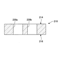
- FIG. 5 schematically shows a top view of a green sheet in which a through hole is formed. Further, FIG. 6 schematically shows a cross-sectional view of the green sheet shown in FIG. 5 along the line BB.
- the green sheet 210 has an upper surface 214 and a lower surface 216. Further, the green sheet 210 is provided with through holes 230a and 230b. The through holes 230a and 230b each penetrate from the upper surface 214 to the lower surface 216 of the green sheet 210.
- the thickness of the green sheet 210 that is, the total length of the through holes 230a and 230b may be in the range of, for example, 200 ⁇ m to 1200 ⁇ m.
- Step S120 Next, a paste for a radiator is prepared.
- the radiator paste is prepared, for example, by mixing metal particles and a vehicle.
- the metal particles may contain at least one of copper, silver, and gold.
- Metal particles for example, a coarse range D 50 is 2 [mu] m ⁇ 7 [mu] m, D 50 may be composed of a fine particle in the range of 0.02 [mu] m ⁇ 1 [mu] m.
- the vehicle contains a resin such as acrylic and / or ethyl cellulose and an organic solvent.
- the organic solvent may be, for example, ⁇ -terepineol.
- the prepared heat-dissipating body paste may be filled into the through holes in 230a and 230b by, for example, a screen printing method.
- FIG. 7 schematically shows a state in which the through holes 230a and 230b are filled with the radiator pastes 240a and 240b, respectively.
- Step S130 a first relaxation paste layer is installed on the upper surface 214 of the green sheet 210 so as to cover the radiator pastes 240a and 240b. Further, a second relaxation paste layer is installed on the lower surface 216 of the green sheet 210 so as to cover the radiator pastes 240a and 240b.
- the first relaxation paste layer and the second relaxation paste layer have the form of a paste containing glass.
- the glass contained in the first relaxation paste layer and the second relaxation paste layer has the coefficient of thermal expansion of the glass contained in the green sheet 210 and the coefficient of thermal expansion of the metal contained in the heat-dissipating pastes 240a and 240b. It has a coefficient of thermal expansion belonging to between.
- the method of installing the first relaxation paste layer and the second relaxation paste layer is not particularly limited.
- the first relaxation paste layer and the second relaxation paste layer may be installed by a printing method.
- the first relaxation paste layer 272 is installed on the upper surface 214 of the green sheet 210, and the second relaxation paste layer 274 is installed on the lower surface 216 of the green sheet 210.
- the cross section is schematically shown.
- Step S140 Next, the assembly 290 formed in step S130 is heat-treated in the atmosphere.
- the temperature of the heat treatment varies depending on the components contained in the assembly 290, but is, for example, in the range of 800 ° C to 1000 ° C.
- FIG. 9 schematically shows a cross section of a sintered member (hereinafter referred to as “sintered substrate 292”) obtained after heat treatment.
- the powders contained in the green sheet 210 are sintered together to form the substrate 130.
- the heat-dissipating body pastes 240a and 240b filled in the through holes 230a and 230b are sintered to form heat-dissipating bodies 258a and 258b, respectively.
- the first relaxation paste layer 272 and the second relaxation paste layer 274 are sintered to form the first relaxation layer 282 and the second relaxation layer 284, respectively.
- Step S150 Next, the first relaxation layer 282 and the second relaxation layer 284 are removed by polishing the upper and lower surfaces of the sintered substrate 292.
- the upper and lower surfaces of the sintered substrate 292 preferably have a surface roughness Ra of 0.5 ⁇ m or less.
- the first substrate 100 as shown in FIGS. 2 and 3 is manufactured.
- the first relaxation paste layer 272 is installed on the upper surface 214 of the green sheet 210, and the second relaxation paste layer 274 is installed on the lower surface 216 of the green sheet 210.
- the solid 290 is heat treated.
- the green sheet 210 (base 130) is arranged in the cooling process of the assembly 290. ) In-plane contraction is hindered. Similarly, the heat-dissipating body pastes 240a and 240b (heat-dissipating bodies 258a and 258b) are prevented from shrinking in the in-plane direction.
- heat radiator 158a even if the relatively large total area S h of 158b, in the course of cooling assembly 290, the substrate 130 and the heat radiating body 158a, at the interface between 158b, hardly cracks can do.
- a substrate for a light emitting element provided with a radiator having a large area can be appropriately manufactured.
- the distance d between the radiator bodies 158a and 158b may be, for example, in the range of 0.35 mm to 0.50 mm.
- Examples 1 to 13 are examples, and Example 21 is a comparative example.
- Example 1 A substrate for a light emitting element was manufactured based on the above-mentioned first manufacturing method.
- the relaxation paste layer was installed by printing a paste containing glass ceramics. The thickness of the relaxation layer was about 10 ⁇ m in each surface.
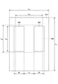
- FIG. 10 schematically shows a top view of the manufactured substrate for a light emitting element (hereinafter referred to as “sample 1”).
- the substrate 310 was a mixed material of glass and ceramics.
- the substrate 310 had dimensions of 1.95 mm in length (referred to as L 1a ), 1.45 mm in width (referred to as L 1b ), and 0.5 mm in thickness.
- the coefficient of thermal expansion of the substrate 310 is about 6 ppm / ° C.
- the mounting portion 365 has dimensions of 1.00 mm in length (referred to as L 2a ) and 1.00 mm in width (referred to as L 2b).
- each radiator body 358 has a length (L 3a ) of 0.92 mm and a width W of 0.36 mm. The distance d between both radiators 358 was set to 0.38 mm. Further, each radiator 358 is arranged so that the outer side surface protrudes from the mounting portion 365 by 0.05 mm.
- Total area S h of the radiator 358 is 0.60 mm 2.
- the area S a of the mounting portion 365 is 1.00 mm 2.
- Overlap area S o is a 0.57mm 2.
- Example 2 to 13 A substrate for a light emitting element was produced by the same method as in Example 1. However, in Examples 2 to 13, as in Example 1, the thickness of the relaxation layer, the total area S h of the radiator, the distance d, and was an overlap area S o and the like are changed.
- the light emitting element substrates manufactured in Examples 2 to 13 are referred to as Samples 2 to 13, respectively.
- Example 21 A substrate for a light emitting element was produced by the same method as in Example 1. However, in this example 21, unlike the case of example 1, the relaxation paste layer was not installed. Therefore, the sintered substrate obtained after the heat treatment of the assembly was used as it is as a substrate for a light emitting element.
- Example 21 the overlap area So was set to 35 mm 2 , and the distance between the two radiators was set to 0.55 mm.
- the substrate for a light emitting element manufactured in Example 21 is referred to as a sample 21.
- the number of observations was 120 for each sample.
- the upper electrode was formed by forming a copper film by an electrolytic plating method.
- the LED element was fixed on the upper electrode of each sample using a die bond material. As a result, a light emitting device was configured.
- the thermal resistance of each light emitting device was measured using a thermal resistance measuring device (TH-2167; manufactured by Mine Koon Denki Co., Ltd.).
Landscapes
- Physics & Mathematics (AREA)
- Condensed Matter Physics & Semiconductors (AREA)
- General Physics & Mathematics (AREA)
- Electromagnetism (AREA)
- Optics & Photonics (AREA)
- Engineering & Computer Science (AREA)
- Microelectronics & Electronic Packaging (AREA)
- Led Device Packages (AREA)
Abstract
発光素子用基板であって、相互に対向する第1の面および第2の面を有し、前記第1の面から前記第2の面に至る貫通孔を有する基体と、前記基体の貫通孔に充填された放熱体と、を有し、前記基体の第1の面は、発光素子が設置される搭載部を有し、当該発光素子用基板は、前記第1の面の側から見たとき、前記放熱体が前記搭載部と重なり合う部分の面積Soが50%以上である、発光素子用基板。
Description
本発明は、発光素子用基板に関する。
発光ダイオード(LED)および半導体レーザダイオード(LD)のような発光素子は、自動車用灯具、ディスプレイ、および街路灯などに幅広く使用されている。発光素子は、発光素子用基板の上に設置され、発光装置として使用される。
一般に、発光素子用基板には、上面(発光素子が設置される表面)から下面にわたって貫通孔が設けられ、この貫通孔には放熱体が充填される。発光素子用基板に放熱体を設けることにより、発光素子で発生した熱を装置外部に逸散させることができる。
近年、ワイヤボンド型に代わる発光装置の構成として、フリップチップボンド型と呼ばれる構造が採用されるようになってきた(例えば特許文献1)。
フリップチップボンド型では、発光素子の底面に設けられた各バンプと、発光素子用基板の上面に設けられた各パッドとにより、電気的接続がなされる。このため、ワイヤボンドタイプの発光装置に比べて、配線長を短くすることができ、発光装置の小型化や高効率化が可能となる。
しかしながら、フリップチップボンド型では、発光素子用基板に充填される放熱体の面積を高めることが難しいと言う問題がある。これは、フリップチップボンド型の場合、発光素子用基板に複数の放熱体を埋め込む必要があり、各放熱体の間の距離が接近すると、発光素子用基板の製造過程でクラックが生じ易くなるためである。
このため、フリップチップボンド型では、発光素子の発熱が改めて問題となる傾向にある。特に、今後、発光装置の小型化がさらに進展すれば、この発熱の問題は、より顕著になることが予想される。
本発明は、このような背景に鑑みなされたものであり、本発明では、従来に比べて良好な放熱性を有する発光素子用基板を提供することを目的とする。
本発明では、発光素子用基板であって、
相互に対向する第1の面および第2の面を有し、前記第1の面から前記第2の面に至る貫通孔を有する基体と、
前記基体の貫通孔に充填された放熱体と、
を有し、
前記基体の第1の面は、発光素子が設置される搭載部を有し、
当該発光素子用基板は、前記第1の面の側から見たとき、前記放熱体が前記搭載部と重なり合う部分の面積Soが50%以上である、発光素子用基板が提供される。
相互に対向する第1の面および第2の面を有し、前記第1の面から前記第2の面に至る貫通孔を有する基体と、
前記基体の貫通孔に充填された放熱体と、
を有し、
前記基体の第1の面は、発光素子が設置される搭載部を有し、
当該発光素子用基板は、前記第1の面の側から見たとき、前記放熱体が前記搭載部と重なり合う部分の面積Soが50%以上である、発光素子用基板が提供される。
本発明では、従来に比べて良好な放熱性を有する発光素子用基板を提供することができる。
以下、図面を参照して、本発明の一実施形態について説明する。
(フリップチップボンド型の発光装置について)
まず、本発明の一実施形態による発光素子用基板の構成および特徴をより良く理解するため、一般的なフリップチップボンド型の発光装置について説明する。
まず、本発明の一実施形態による発光素子用基板の構成および特徴をより良く理解するため、一般的なフリップチップボンド型の発光装置について説明する。
図1には、一般的なフリップチップボンド型の発光装置の断面構成を概略的に示す。
図1に示すように、この発光装置1は、発光素子用基板2と、発光素子60とを有する。
発光素子用基板2は、上面4および下面6を有し、発光素子60は、発光素子用基板2の上面4の側に設置される。
発光素子用基板2は、基体10と、複数の放熱体18とを有する。基体10は、上面14から下面16に貫通する複数の貫通孔を有し、放熱体18は、各貫通孔に充填されている。なお、基体10の上面14および下面16は、それぞれ、発光素子用基板2の上面4および下面6に対応する。
発光装置1は、さらに、発光素子用基板2の上面4に形成された複数の上部電極25と、下面6に形成された下部導体35とを有する。上部電極25および下部導体35は、対象の放熱体18と電気的に接続されるように配置される。
また、発光装置1は、発光素子60の底部62に、複数の電極バンプ65を有する。各電極バンプ65は、それぞれの上部電極25と接続される。
このような構造を有する発光装置1では、ワイヤボンド型の装置とは異なり、発光素子60の任意の位置で通電を行うことができる。このため、発光装置1では、配線長を短くすることができる上、装置を小型化することができる。
ここで、放熱体18は、発光素子60で生じた熱を、下部導体35を介して外部に逸散させる役割を有する。従って、放熱効率の観点から、発光装置1の上側(発光素子60の側)から放熱体18を見た場合(以下、「上面視」と称する)、各放熱体18の面積は、できるだけ大きくすることが望ましい。
しかしながら、発光素子用基板2は、通常、基体10のベースとなるグリーンシートに設けられた貫通孔に放熱体18用のペーストを充填した状態で、グリーンシートを熱処理することにより製造される。グリーンシート(または基体10)と放熱体ペースト(または放熱体18)とは熱膨張係数が異なるため、熱処理の際に、両者の界面に応力が生じる。特に、放熱体18の領域を広げた場合、この応力の影響が無視できなくなり、基体10の加熱/冷却の工程で、基体10と放熱体18との界面にクラックが生じてしまう。
このように、放熱体18の面積の拡張には限界があり、その結果、発光装置1の放熱特性のいっそうの向上は難しいという問題がある。
これに対して、本発明の一実施形態では、以降に詳しく示すように、放熱体18の面積をより拡張することができる。例えば、本発明の一実施形態では、上面視、放熱体18が発光素子60と重なり合う面積の総和(以下、「オーバーラップ面積」と称する)Soを、50%以上にすることができる。
従って、本発明の一実施形態では、発光装置1の放熱特性を有意に高めることが可能となる。
(本発明の一実施形態による発光素子用基板)
次に、図2~図3を参照して、本発明の一実施形態による発光素子用基板の構成例について説明する。
次に、図2~図3を参照して、本発明の一実施形態による発光素子用基板の構成例について説明する。
図2には、本発明の一実施形態による発光素子用基板の模式的な上面図を示す。また、図3には、図2に示した発光素子用基板のA-A線に沿った断面を模式的に示す。
図2および図3に示すように、本発明の一実施形態による発光素子用基板(以下、「第1の基板」と称する)100は、相互に対向する第1の面104および第2の面106を有する。また、第1の基板100は、基体130と、複数の放熱体158とを有する。なお、図2および図3に示した例では、2つの放熱体158が示されており、以降、これらを、それぞれ、158aおよび158bで表す。
基体130は、相互に対向する上面134および下面136を有する。また、基体130は、上面134から下面136に至る複数の貫通孔148a、148bを有する。
放熱体158a、158bは、基体130のそれぞれの貫通孔148a、148bに充填されており、従って、上面134から下面136まで延伸する。
第1の基板100の第1の面104は、基体130の上面134の側に対応し、第1の基板100の第2の面106は、基体130の下面136の側に対応する。
第1の基板100の第1の面104は、発光素子(図示されていない)が設置される搭載部165を有する。図2において、搭載部165は、四角形状の破線で示されている。
ここで、第1の基板100は、第1の面104の側から見たとき、すなわち、第1の基板100の上面視、放熱体158a、158bが搭載部165と重なり合う部分の面積、すなわちオーバーラップ面積Soが50%以上であるという特徴を有する。
オーバーラップ面積Soは、例えば、60%以上であり、65%以上であることが好ましい。
このような特徴を有する第1の基板100の上に発光素子を設置して発光装置を構成した場合、発光素子で生じた熱を、放熱体158a、158bを介して外部に有効に逸散させることが可能となる。
従って、そのような発光装置では、従来に比べて放熱特性を高めることが可能となる。
なお、図2および図3に示した例では、第1の基板100は、上面視、2つの矩形状の放熱体158a、158bを有する。しかしながら、これは単なる一例であって、放熱体158の数は、複数である限り、特に限られない。また、放熱体158の形状は、特に限られない。
例えば、放熱体158の形状は、略円形、略楕円形、または略n角形(ただしnは、3以上の整数)であってもよい。また、放熱体158は、コーナー部がラウンドされた形状を有してもよい。さらに、各放熱体158は、必ずしも同一の形状である必要はなく、相互に異なる形状を有してもよい。
同様に、図2に示した例では、搭載部165は、矩形状の形態を有する。しかしながら、搭載部165の形状は、特に限られず、搭載部165は、例えば、略円形、略楕円形、または略n角形(ただしnは、3以上の整数)の形状を有してもよい。また、搭載部165は、コーナー部がラウンドされた形状を有してもよい。
(各構成部材)
次に、本発明の一実施形態による発光素子用基板に含まれる各構成部材について説明する。
次に、本発明の一実施形態による発光素子用基板に含まれる各構成部材について説明する。
なお、ここでは明確化のため、図2および図3に示した第1の基板100を例に、その構成部材について説明する。従って、各部材を表す際には、図2および図3に示した参照符号を使用する。
(基体130)
基体130は、例えば、ガラスを主体とした材料で構成される。基体130は、ガラスとセラミックスの混合材料で構成されてもよい。
基体130は、例えば、ガラスを主体とした材料で構成される。基体130は、ガラスとセラミックスの混合材料で構成されてもよい。
ガラスの組成は、特に限られないが、例えば、SiO2、B2O3、CaO、およびAl2O3を含む組成が好ましい。ガラスは、さらに、K2OおよびNa2Oの少なくとも一方を含んでも良い。
このような組成とすることにより、基体130と放熱体158との密着性が向上する。
このうち、SiO2は、ガラスのネットワークフォーマとなる物質である。SiO2は、ガラス中に、57mol%~65mol%の範囲で含まれることが好ましい。
SiO2の含有量が57mol%未満の場合、安定なガラスを得ることが難しくなるとともに、化学的耐久性が低下するおそれがある。一方、SiO2の含有量が65mol%を超えると、ガラス溶融温度およびガラス転移温度Tgが過度に高くなるおそれある。SiO2の含有量は、好ましくは58mol%以上、より好ましくは59mol%以上、特に好ましくは60mol%以上である。また、SiO2の含有量は、好ましくは64mol%以下、より好ましくは63mol%以下である。
B2O3は、ガラスのネットワークフォーマとなる物質である。B2O3は、ガラス中に、13mol%~18mol%の範囲で含まれることが好ましい。
B2O3の含有量が13mol%未満の場合、ガラス溶融温度およびガラス転移温度Tgが過度に高くなるおそれがある。一方、B2O3の含有量が18mol%を超えると、安定なガラスを得ることが難しくなるとともに、化学的耐久性が低下するおそれがある。B2O3の含有量は、好ましくは14mol%以上、より好ましくは15mol%以上である。また、B2O3の含有量は、好ましくは17mol%以下、より好ましくは16mol%以下である。
CaOは、ガラスの安定性や結晶の析出性を高めるとともに、ガラス溶融温度およびガラス転移温度Tgを低下させるために添加される。CaOは、ガラス中に、9mol%~23mol%の範囲で含まれることが好ましい。
CaOの含有量が9mol%未満の場合、ガラス溶融温度が過度に高くなるおそれがある。一方、CaOの含有量が23mol%を超えると、ガラスが不安定となるおそれがある。CaOの含有量は、好ましくは12mol%以上、より好ましくは13mol%以上、特に好ましくは14mol%以上である。また、CaOの含有量は、好ましくは22mol%以下、より好ましくは21mol%以下、特に好ましくは20mol%以下である。
Al2O3は、ガラスの安定性、化学的耐久性、および強度を高めるために添加される。Al2O3は、ガラス中に、3mol%~8mol%の範囲で含まれることが好ましい。
Al2O3の含有量が3mol%未満の場合、ガラスが不安定となるおそれがある。一方、Al2O3の含有量が8mol%を超える場合、ガラス溶融温度およびガラス転移温度Tgが過度に高くなるおそれがある。Al2O3の含有量は、好ましくは4mol%以上、より好ましくは5mol%以上である。また、Al2O3の含有量は、好ましくは7mol%以下、より好ましくは6mol%以下である。
K2O、Na2Oは、ガラス転移温度Tgを低下させる。K2OおよびNa2Oは、ガラス中に、合計で0.5mol%~6mol%の範囲で含まれることが好ましい。
K2OおよびNa2Oの合計含有量が0.5mol%未満の場合、ガラス溶融温度およびガラス転移温度Tgが過度に高くなるおそれがある。一方、K2OおよびNa2Oの合計含有量が6mol%を超える場合、化学的耐久性、特に耐酸性が低下するおそれがあり、電気的絶縁性も低下するおそれがある。K2OおよびNa2Oの合計含有量は、0.8mol%以上5mol%以下が好ましい。
なお、ガラスの組成は、必ずしも上記成分のみからなるものに限定されず、他の成分を含有してもよい。他の成分を含有する場合、その合計した含有量は10mol%以下が好ましい。
基体130がセラミックスを含む場合、セラミックスとしては、これに限られるものではないが、例えば、アルミナ、ジルコニア、または両者の混合物などが使用される。
基体130に含まれるガラスの量は、例えば、基体130全体に対して35質量%~75質量%の範囲である。ガラスの量は、基体130全体に対して40質量%~70質量%の範囲であることが好ましい。
基体130の厚さは、特に限られないが、例えば、200μm~1200μmの範囲である。
基体130の上面134および/または下面136は、表面粗さRaが0.5μm以下であることが好ましい。この場合、基体130の上面134および/または下面136に加わる局部的な応力の集中が抑制され、クラックの発生をより抑制することが可能となる。
(放熱体158)
放熱体158は、熱伝導性および電気伝導性を有し、金属を含む。放熱体158は、例えば、銅、銀、および金の少なくとも一つを含んでもよい。
放熱体158は、熱伝導性および電気伝導性を有し、金属を含む。放熱体158は、例えば、銅、銀、および金の少なくとも一つを含んでもよい。
第1の基板100の上面視、放熱体158の総面積Shは、例えば、0.5mm2~1.5mm2の範囲である。
ここで、総面積Shは、それぞれの放熱体158の面積の合計で表される。例えば、図2および図3に示した例では、総面積Shは、第1の基板100の上面視、放熱体158aの面積と、放熱体158bの面積との和で表される。
第1の基板100が複数の放熱体158を有する場合、上面視、隣接する放熱体158同士の距離d(図2参照)は、例えば、0.50mm以下である。距離dは、0.40mm以下であることが好ましく、0.35mm以下であることがより好ましい。
なお、本願において、距離dは、上面視、隣り合う放熱体の間の最小寸法として定められる。
(搭載部165)
前述のように、搭載部165の形状は特に限られず、搭載部165として、各種形状を採用することができる。
前述のように、搭載部165の形状は特に限られず、搭載部165として、各種形状を採用することができる。
搭載部165の面積Saは、特に限られないが、例えば、0.15mm2~4.00mm2の範囲である。搭載部165の面積Saは、0.50mm2~2.00mm2の範囲であることが好ましく、0.75mm2~1.25mm2の範囲であることがより好ましい。
(第1の基板100)
上記説明では、第1の基板100は、基体130と放熱体158とで構成される。
上記説明では、第1の基板100は、基体130と放熱体158とで構成される。
しかしながら、第1の基板100は、さらに、図1に示したような、複数の上部電極25を有してもよい。上部電極25は、各放熱体158a、158bの上部を覆うようにして、基体130の上面134に設置される。
また、第1の基板100は、さらに、図1に示したような、複数の下部導体35を有してもよい。下部導体35は、各放熱体158a、158bの底面を覆うようにして、基体130の下面136に設置される。
上部電極25および下部導体35は、従来から知られている、いかなる方法で設置されてもよい。例えば、上部電極25および下部導体35は、基体130の上面134および下面136に導体ペーストを設置した状態で、基体130を焼成することにより形成されてもよい。
また、上記説明では、第1の基板100は、単一の発光素子用の基板として提供される。すなわち、第1の基板100は、一つの発光装置用の放熱体158の組のみを有する。
しかしながら、これとは別に、第1の基板100は、複数の発光装置用の基板として、提供されてもよい。例えば、第1の基板100は、第1の発光装置用の基体130部分および放熱体158部分と、第2の発光装置用の基体130部分および放熱体158部分とを有してもよい。この場合、第1の基板100は、後に所定の位置で切断して、それぞれの発光装置用に利用される。
この他にも、当業者には各種変更および追加が想定され得る。
(本発明の一実施形態による発光素子用基板の適用例)
本発明の一実施形態による発光素子用基板は、例えば、図1に示したようなフリップチップボンド型の発光装置1用の発光素子用基板として使用される。
本発明の一実施形態による発光素子用基板は、例えば、図1に示したようなフリップチップボンド型の発光装置1用の発光素子用基板として使用される。
係る発光装置1において、発光素子60は、いかなるタイプであってもよい。発光素子60は、例えば、LED素子、LD、または面発光レーザダイオード(VCSEL)等であってもよい。
本発明の一実施形態による発光素子用基板を備える発光装置1では、放熱特性を有意に高めることができる。
(本発明の一実施形態による発光素子用基板の製造方法)
次に、図4~図9を参照して、本発明の一実施形態による発光素子用基板の製造方法の一例について説明する。
次に、図4~図9を参照して、本発明の一実施形態による発光素子用基板の製造方法の一例について説明する。
図4には、本発明の一実施形態による発光素子用基板を製造する方法のフローを模式的に示す。
図4に示すように、本発明の一実施形態による発光素子用基板を製造する方法(以下、「第1の製造方法」と称する)は、
上面および下面を有するグリーンシートに複数の貫通孔を形成する工程(S110)と、
各貫通孔に、放熱体用ペーストを充填する工程(S120)と、
グリーンシートの上面および下面に、緩和ペースト層を設置する工程(S130)と、
グリーンシートを熱処理して、焼結基板を形成する工程(S140)と、
前記焼結基板の上下面を研磨して、発光素子用基板を得る工程(S150)と、
を有する。
上面および下面を有するグリーンシートに複数の貫通孔を形成する工程(S110)と、
各貫通孔に、放熱体用ペーストを充填する工程(S120)と、
グリーンシートの上面および下面に、緩和ペースト層を設置する工程(S130)と、
グリーンシートを熱処理して、焼結基板を形成する工程(S140)と、
前記焼結基板の上下面を研磨して、発光素子用基板を得る工程(S150)と、
を有する。
以下、図5~図9を参照して、各工程について、より詳しく説明する。
なお、ここでは、前述の第1の基板100を例に、その製造方法について説明する。従って、各部材を表す際には、図2および図3に使用した参照符号を使用する。
(工程S110)
まず、グリーンシートが準備される。グリーンシートは、ガラスを主体とする材料で構成される。グリーンシートは、さらに、セラミックスおよび/または有機バインダを含んでもよい。
まず、グリーンシートが準備される。グリーンシートは、ガラスを主体とする材料で構成される。グリーンシートは、さらに、セラミックスおよび/または有機バインダを含んでもよい。
グリーンシートは、例えば、以下の工程を経て作製される。
(ガラス粉末の作製)
ガラス粉末は、所定の組成を有するガラスを粉砕することにより調製できる。ガラス粉末は、前述のような組成を有してもよい。
ガラス粉末は、所定の組成を有するガラスを粉砕することにより調製できる。ガラス粉末は、前述のような組成を有してもよい。
ガラスの粉砕には、乾式粉砕法または湿式粉砕法のいずれを使用しても良い。
湿式粉砕法では、溶媒中でガラスが粉砕される。溶媒には、水を用いることが好ましい。粉砕は、例えばロールミル、ボールミル、またはジェットミル等の粉砕機が使用できる。
粉砕処理後に得られるガラス粉末の50%平均粒径(D50)は、0.5μm以上2μm以下が好ましい。
なお、本願において、50%平均粒径(D50)は、レーザ回折散乱法による粒子径測定装置により得られる値をいう。
ガラス粉末のD50が0.5μm以上の場合、ガラス粉末が凝集しにくく、取り扱いが容易であるとともに、均一に分散させることができる。一方、ガラス粉末のD50が2μm以下の場合、ガラス軟化温度の上昇や焼結不足が抑制される。粒径の調整は、分級等により行われる。
(セラミックス粉末の作製)
セラミックス粉末としては、一般的なガラスセラミックスの製造に用いられるものが使用できる。セラミックス粉末としては、例えば、アルミナ粉末、ジルコニア粉末、またはアルミナ粉末とジルコニア粉末との混合物が好適に使用できる。
セラミックス粉末としては、一般的なガラスセラミックスの製造に用いられるものが使用できる。セラミックス粉末としては、例えば、アルミナ粉末、ジルコニア粉末、またはアルミナ粉末とジルコニア粉末との混合物が好適に使用できる。
セラミックス粉末のD50は、例えば、0.5μm以上4μm以下が好ましい。
(グリーンシートの作製)
次に、前述のガラス粉末と、セラミックス粉末と、有機バインダとが所定の割合で混合され、グリーンシート用スラリーが調製される。
次に、前述のガラス粉末と、セラミックス粉末と、有機バインダとが所定の割合で混合され、グリーンシート用スラリーが調製される。
有機バインダとしては、ポリビニルブチラール、および/またはアクリル樹脂等が使用できる。
グリーンシート用スラリーには、さらに、可塑剤、分散剤、および/または溶剤等が添加されても良い。可塑剤としては、フタル酸ジブチル、フタル酸ジオクチル、および/またはフタル酸ブチルベンジル等が使用できる。また、溶剤としては、トルエン、キシレン、2-プロパノール、および/または2-ブタノール等の有機溶剤が使用できる。
調製されるグリーンシート用スラリーにおいて、ガラス粉末とセラミックス粉末との質量比(ガラス:セラミックス)は、35:65~75:25の範囲であることが好ましい。
得られたグリーンシート用スラリーは、ドクターブレード法等によりシート状に成形される。
その後、グリーンシート用スラリーが乾燥され、グリーンシートが形成される。グリーンシートは、複数枚を積層した状態で、次の貫通孔形成工程に供されても良い。なお、次の貫通孔形工程以降、単一のグリーンシートも、複数枚積層して構成されたグリーンシートも、単に「グリーンシート」と称する。
次に、グリーンシートに複数の貫通孔が形成される。貫通孔の形成方法は、特に限られず、従来の一般的な方法により、形成されてもよい。
図5には、貫通孔が形成されたグリーンシートの上面図を模式的に示す。また、図6には、図5に示したグリーンシートのB-B線に沿った断面図を模式的に示す。
グリーンシート210は、上面214および下面216を有する。また、グリーンシート210には、貫通孔230aおよび230bが設けられる。貫通孔230aおよび230bは、それぞれ、グリーンシート210の上面214から下面216まで貫通する。
グリーンシート210の厚さ、すなわち貫通孔230aおよび230bの全長は、例えば、200μm~1200μmの範囲であってもよい。
(工程S120)
次に、放熱体用ペーストが調製される。
次に、放熱体用ペーストが調製される。
放熱体用ペーストは、例えば、金属粒子およびビヒクルを混合することにより調製される。
金属粒子は、銅、銀、および金の少なくとも一つを含んでもよい。金属粒子は、例えば、D50が2μm~7μmの範囲の粗粒と、D50が0.02μm~1μmの範囲の細粒とで構成されても良い。
ビヒクルは、アクリルおよび/またはエチルセルロース等の樹脂と、有機溶剤とを含む。有機溶剤は、例えばαテレピネオールであっても良い。
調製された放熱体用ペーストは、例えば、スクリーン印刷法により、貫通孔に230a、230bに充填されても良い。
図7には、各貫通孔230aおよび230bに、それぞれ、放熱体用ペースト240aおよび240bが充填された状態を模式的に示す。
(工程S130)
次に、グリーンシート210の上面214に、放熱体用ペースト240aおよび240bを覆うように、第1の緩和ペースト層が設置される。また、グリーンシート210の下面216に、放熱体用ペースト240aおよび240bを覆うように、第2の緩和ペースト層が設置される。
次に、グリーンシート210の上面214に、放熱体用ペースト240aおよび240bを覆うように、第1の緩和ペースト層が設置される。また、グリーンシート210の下面216に、放熱体用ペースト240aおよび240bを覆うように、第2の緩和ペースト層が設置される。
第1の緩和ペースト層および第2の緩和ペースト層は、ガラスを含むペーストの形態を有する。
なお、第1の緩和ペースト層および第2の緩和ペースト層に含まれるガラスは、グリーンシート210に含まれるガラスの熱膨張係数と、放熱体用ペースト240a、240bに含まれる金属の熱膨張係数との間に属する熱膨張係係数を有する。
第1の緩和ペースト層および第2の緩和ペースト層の設置方法は、特に限られない。例えば、第1の緩和ペースト層および第2の緩和ペースト層は、印刷法により設置されてもよい。
図8には、グリーンシート210の上面214に、第1の緩和ペースト層272が設置され、グリーンシート210の下面216に、第2の緩和ペースト層274が設置されて構成された組立体290の断面を模式的に示す。
(工程S140)
次に、工程S130で形成された組立体290が、大気中で熱処理される。
次に、工程S130で形成された組立体290が、大気中で熱処理される。
熱処理の温度は、組立体290に含まれる成分によっても変化するが、例えば、800℃~1000℃の範囲である。
図9には、熱処理後に得られる焼結部材(以下、「焼結基板292」と称する)の断面を模式的に示す。
熱処理により、グリーンシート210に含まれる粉末同士が焼結し、基体130が形成される。また、貫通孔230a、230bに充填された放熱体用ペースト240aおよび240bが焼結して、それぞれ、放熱体258a、258bが形成される。さらに、第1の緩和ペースト層272および第2の緩和ペースト層274が焼結して、それぞれ、第1の緩和層282および第2の緩和層284が形成される。
(工程S150)
次に、焼結基板292の上下面を研磨することにより、第1の緩和層282および第2の緩和層284が除去される。
次に、焼結基板292の上下面を研磨することにより、第1の緩和層282および第2の緩和層284が除去される。
研磨後に、焼結基板292の上下面は、表面粗さRaが0.5μm以下となることが好ましい。
以上の工程により、図2および図3に示したような第1の基板100が製造される。
ここで、第1の製造方法では、グリーンシート210の上面214に第1の緩和ペースト層272が設置され、グリーンシート210の下面216に第2の緩和ペースト層274が設置された状態で、組立体290が熱処理される。
この場合、第1の緩和ペースト層272および第2の緩和ペースト層274は、グリーンシート210の面内方向に沿って配置されているため、組立体290の冷却過程において、グリーンシート210(基体130)の面内方向の収縮が妨げられる。同様に、放熱体用ペースト240a、240b(放熱体258a、258b)は、面内方向の収縮が妨げられる。
従って、上面視、放熱体158a、158bの総面積Shが比較的大きい場合であっても、組立体290の冷却過程において、基体130と放熱体158a、158bとの界面において、クラックを生じ難くすることができる。
また、放熱体158a、158bの間の距離dを小さくすることも可能となる。
その結果、第1の製造方法では、大きな面積を有する放熱体を備える発光素子用基板を、適正に製造することができる。
具体的には、前述のように、上面視、50%以上のオーバーラップ面積Soを有する発光素子用基板を得ることが可能となる。放熱体158a、158bの間の距離dは、例えば、0.35mm~0.50mmの範囲であってもよい。
次に、本発明の具体的な実施例について説明する。なお、以下の説明において、例1~例13は、実施例であり、例21は、比較例である。
(例1)
前述の第1の製造方法に基づいて、発光素子用基板を作製した。
前述の第1の製造方法に基づいて、発光素子用基板を作製した。
発光素子用基板は、グリーンシート、放熱体用ペースト、および緩和ペースト層を含む組立体を大気中で熱処理して焼結基板を形成した後、両面の緩和層(熱膨張係数=15.0ppm/℃)を除去することにより作製した。なお、緩和ペースト層は、ガラスセラミックスを含むペーストを印刷することにより設置した。緩和層の厚さは、それぞれの面で約10μmであった。
図10には、作製された発光素子用基板(以下、「サンプル1」と称する)の上面図を模式的に示す。
基体310は、ガラスとセラミックスの混合材料とした。基体310は、縦(L1aとする)1.95mm、横(L1bとする)1.45mm、厚さ0.5mmの寸法であった。基体310の熱膨張係数は、約6ppm/℃である。
放熱体358には、銀(熱膨張係数=19.7ppm/℃)を使用した。
図10には、基体310の上面における搭載部365の形状を破線で示した。搭載部365は、縦(L2aとする)1.00mm、横(L2bとする)1.00mmの寸法である。
また、各放熱体358は、縦(L3aとする)が0.92mm、幅Wが0.36mmである。なお、両方の放熱体358の間の距離dは、0.38mmとした。また、各放熱体358は、外側の側辺が、搭載部365から0.05mmだけはみ出るように配置した。
放熱体358の総面積Shは、0.60mm2である。一方、搭載部365の面積Saは、1.00mm2である。オーバーラップ面積Soは、0.57mm2である。
(例2~例13)
例1と同様の方法により、発光素子用基板を作製した。ただし、例2~例13では、例1の場合とは、緩和層の厚さ、放熱体の総面積Sh、距離d、およびオーバーラップ面積So等を変化させた。
例1と同様の方法により、発光素子用基板を作製した。ただし、例2~例13では、例1の場合とは、緩和層の厚さ、放熱体の総面積Sh、距離d、およびオーバーラップ面積So等を変化させた。
例2~例13において製造された発光素子用基板を、それぞれ、サンプル2~サンプル13と称する。
(例21)
例1と同様の方法により、発光素子用基板を作製した。ただし、この例21では、例1の場合とは異なり、緩和ペースト層は、設置しなかった。従って、組立体の熱処理後に得られた焼結基板をそのまま、発光素子用基板とした。
例1と同様の方法により、発光素子用基板を作製した。ただし、この例21では、例1の場合とは異なり、緩和ペースト層は、設置しなかった。従って、組立体の熱処理後に得られた焼結基板をそのまま、発光素子用基板とした。
また、例21では、オーバーラップ面積Soを35mm2するとともに、2つの放熱体の間の距離を、0.55mmとした。
例21において製造された発光素子用基板を、サンプル21と称する。
以下の表1には、各サンプルにおける特徴をまとめて示した。

各サンプルを用いて、以下の評価を実施した。
(クラック発生率の評価)
目視により、サンプルの上面から下面にわたって延在するクラックの発生率を評価した。
目視により、サンプルの上面から下面にわたって延在するクラックの発生率を評価した。
観察数は、それぞれのサンプルに対して、120個とした。
(熱抵抗の測定)
それぞれのサンプルの搭載部にLED素子を配置して、発光装置を作製した。
それぞれのサンプルの搭載部にLED素子を配置して、発光装置を作製した。
まず、各サンプルの上面に、それぞれの放熱体を覆うように、2つの上部電極を形成した。上部電極は、電解めっき法により銅を成膜することにより形成した。
次に、ダイボンド材を用いて、LED素子を、各サンプルの上部電極上に固定した。これにより、発光装置が構成された。
各発光装置の熱抵抗を、熱抵抗測定器(TH-2167;嶺光音電機社製)を用いて測定した。
以下の表2には、各サンプルにおいて得られた評価結果をまとめて示した。
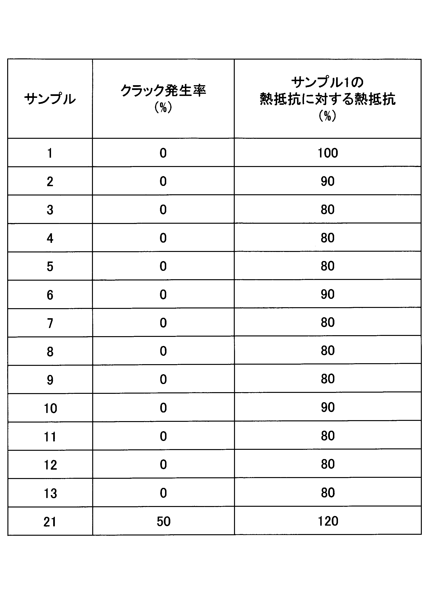
これに対して、作製の際に緩和層を利用したサンプル1~サンプル13では、基体と放熱体との界面でのクラックの発生が有意に抑制されていることが確認された。
また、サンプル1~サンプル13では、熱抵抗が有意に低減されることが確認された。
本願は、2020年7月15日に出願した日本国特許出願第2020-121684号に基づく優先権を主張するものであり、同日本国出願の全内容を本願に参照により援用する。
1 フリップチップボンド型の発光装置
2 発光素子用基板
4 上面
6 下面
10 基体
14 上面
16 下面
18 放熱体
25 上部電極
35 下部導体
60 発光素子
62 底部
65 電極バンプ
100 発光素子用基板(第1の基板)
104 第1の面
106 第2の面
130 基体
134 上面
136 下面
148a、148b 貫通孔
158、158a、158b 放熱体
165 搭載部
210 グリーンシート
214 上面
216 下面
230a、230b 貫通孔
240a、240b 放熱体用ペースト
258a、258b 放熱体
272 第1の緩和ペースト層
274 第2の緩和ペースト層
282 第1の緩和層
284 第2の緩和層
290 組立体
292 焼結基板
310 基体
358 放熱体
365 搭載部
2 発光素子用基板
4 上面
6 下面
10 基体
14 上面
16 下面
18 放熱体
25 上部電極
35 下部導体
60 発光素子
62 底部
65 電極バンプ
100 発光素子用基板(第1の基板)
104 第1の面
106 第2の面
130 基体
134 上面
136 下面
148a、148b 貫通孔
158、158a、158b 放熱体
165 搭載部
210 グリーンシート
214 上面
216 下面
230a、230b 貫通孔
240a、240b 放熱体用ペースト
258a、258b 放熱体
272 第1の緩和ペースト層
274 第2の緩和ペースト層
282 第1の緩和層
284 第2の緩和層
290 組立体
292 焼結基板
310 基体
358 放熱体
365 搭載部
Claims (6)
- 発光素子用基板であって、
相互に対向する第1の面および第2の面を有し、前記第1の面から前記第2の面に至る貫通孔を有する基体と、
前記基体の貫通孔に充填された放熱体と、
を有し、
前記基体の第1の面は、発光素子が設置される搭載部を有し、
当該発光素子用基板は、前記第1の面の側から見たとき、前記放熱体が前記搭載部と重なり合う部分の面積Soが50%以上である、発光素子用基板。 - 前記放熱体は、第1の放熱体および第2の放熱体を有し、
第1の放熱体と第2の放熱体の間の距離は、0.5mm以下である、請求項1に記載の発光素子用基板。 - 前記第1の面および/または前記第2の面は、表面粗さRaが0.5μm以下である、請求項1または2に記載の発光素子用基板。
- 前記基体は、ガラスを含む、請求項1乃至3のいずれか一つに記載の発光素子用基板。
- 前記基体は、セラミックスを含む、請求項4に記載の発光素子用基板。
- 前記放熱体は、金属を含む、請求項1乃至5のいずれか一つに記載の発光素子用基板。
Priority Applications (1)
| Application Number | Priority Date | Filing Date | Title |
|---|---|---|---|
| JP2022536278A JP7697468B2 (ja) | 2020-07-15 | 2021-07-06 | 発光素子用基板、および発光素子用基板の製造方法 |
Applications Claiming Priority (2)
| Application Number | Priority Date | Filing Date | Title |
|---|---|---|---|
| JP2020-121684 | 2020-07-15 | ||
| JP2020121684 | 2020-07-15 |
Publications (1)
| Publication Number | Publication Date |
|---|---|
| WO2022014411A1 true WO2022014411A1 (ja) | 2022-01-20 |
Family
ID=79555382
Family Applications (1)
| Application Number | Title | Priority Date | Filing Date |
|---|---|---|---|
| PCT/JP2021/025474 Ceased WO2022014411A1 (ja) | 2020-07-15 | 2021-07-06 | 発光素子用基板 |
Country Status (3)
| Country | Link |
|---|---|
| JP (1) | JP7697468B2 (ja) |
| TW (1) | TW202205701A (ja) |
| WO (1) | WO2022014411A1 (ja) |
Citations (12)
| Publication number | Priority date | Publication date | Assignee | Title |
|---|---|---|---|---|
| JP2006229151A (ja) * | 2005-02-21 | 2006-08-31 | Kyocera Corp | 発光素子用配線基板ならびに発光装置 |
| JP2010080800A (ja) * | 2008-09-29 | 2010-04-08 | Seiko Instruments Inc | 発光デバイス及びその製造方法 |
| US20100090239A1 (en) * | 2008-10-13 | 2010-04-15 | Advanced Optoelectronic Technology Inc. | Ceramic package structure of high power light emitting diode and manufacturing method thereof |
| JP2011060859A (ja) * | 2009-09-07 | 2011-03-24 | Seiko Instruments Inc | 電子部品の製造方法および電子部品 |
| US20120043576A1 (en) * | 2010-08-17 | 2012-02-23 | Advanced Optoelectronic Technology, Inc. | Led package structure |
| WO2012086724A1 (ja) * | 2010-12-24 | 2012-06-28 | 旭硝子株式会社 | 連結基板およびその製造方法、並びに素子基板、発光装置 |
| WO2013002348A1 (ja) * | 2011-06-30 | 2013-01-03 | 旭硝子株式会社 | 発光素子用基板および発光装置 |
| JP2013065793A (ja) * | 2011-09-20 | 2013-04-11 | Ngk Spark Plug Co Ltd | 配線基板 |
| JP2015115532A (ja) * | 2013-12-13 | 2015-06-22 | 京セラ株式会社 | 発光素子搭載用基板およびそれを備えた発光装置 |
| US20180076370A1 (en) * | 2015-04-10 | 2018-03-15 | Osram Opto Semiconductors Gmbh | Light-emitting component and method of producing a light-emitting component |
| US20190181314A1 (en) * | 2005-10-19 | 2019-06-13 | Lg Innotek Co., Ltd. | Light emitting diode package having frame with bottom surface having two surfaces different in height |
| JP2019114624A (ja) * | 2017-12-22 | 2019-07-11 | スタンレー電気株式会社 | 半導体発光装置及びその製造方法 |
Family Cites Families (3)
| Publication number | Priority date | Publication date | Assignee | Title |
|---|---|---|---|---|
| JP2013127996A (ja) * | 2010-03-29 | 2013-06-27 | Sanyo Electric Co Ltd | 発光装置及び発光装置モジュール |
| JP5124688B2 (ja) * | 2011-03-16 | 2013-01-23 | 有限会社 ナプラ | 照明装置、ディスプレイ、及び信号灯 |
| JP6627495B2 (ja) * | 2015-12-25 | 2020-01-08 | Agc株式会社 | 深紫外発光素子用基板、深紫外発光素子用連結基板、および深紫外発光装置 |
-
2021
- 2021-07-06 JP JP2022536278A patent/JP7697468B2/ja active Active
- 2021-07-06 WO PCT/JP2021/025474 patent/WO2022014411A1/ja not_active Ceased
- 2021-07-09 TW TW110125319A patent/TW202205701A/zh unknown
Patent Citations (12)
| Publication number | Priority date | Publication date | Assignee | Title |
|---|---|---|---|---|
| JP2006229151A (ja) * | 2005-02-21 | 2006-08-31 | Kyocera Corp | 発光素子用配線基板ならびに発光装置 |
| US20190181314A1 (en) * | 2005-10-19 | 2019-06-13 | Lg Innotek Co., Ltd. | Light emitting diode package having frame with bottom surface having two surfaces different in height |
| JP2010080800A (ja) * | 2008-09-29 | 2010-04-08 | Seiko Instruments Inc | 発光デバイス及びその製造方法 |
| US20100090239A1 (en) * | 2008-10-13 | 2010-04-15 | Advanced Optoelectronic Technology Inc. | Ceramic package structure of high power light emitting diode and manufacturing method thereof |
| JP2011060859A (ja) * | 2009-09-07 | 2011-03-24 | Seiko Instruments Inc | 電子部品の製造方法および電子部品 |
| US20120043576A1 (en) * | 2010-08-17 | 2012-02-23 | Advanced Optoelectronic Technology, Inc. | Led package structure |
| WO2012086724A1 (ja) * | 2010-12-24 | 2012-06-28 | 旭硝子株式会社 | 連結基板およびその製造方法、並びに素子基板、発光装置 |
| WO2013002348A1 (ja) * | 2011-06-30 | 2013-01-03 | 旭硝子株式会社 | 発光素子用基板および発光装置 |
| JP2013065793A (ja) * | 2011-09-20 | 2013-04-11 | Ngk Spark Plug Co Ltd | 配線基板 |
| JP2015115532A (ja) * | 2013-12-13 | 2015-06-22 | 京セラ株式会社 | 発光素子搭載用基板およびそれを備えた発光装置 |
| US20180076370A1 (en) * | 2015-04-10 | 2018-03-15 | Osram Opto Semiconductors Gmbh | Light-emitting component and method of producing a light-emitting component |
| JP2019114624A (ja) * | 2017-12-22 | 2019-07-11 | スタンレー電気株式会社 | 半導体発光装置及びその製造方法 |
Also Published As
| Publication number | Publication date |
|---|---|
| JPWO2022014411A1 (ja) | 2022-01-20 |
| TW202205701A (zh) | 2022-02-01 |
| JP7697468B2 (ja) | 2025-06-24 |
Similar Documents
| Publication | Publication Date | Title |
|---|---|---|
| US8319240B2 (en) | Light-emitting device | |
| KR102163532B1 (ko) | 반도체 장치, 세라믹스 회로 기판 및 반도체 장치의 제조 방법 | |
| EP2369903A1 (en) | Substrate for light-emitting element and light-emitting device | |
| CN1815720A (zh) | 半导体器件及其制造方法 | |
| JP6146007B2 (ja) | 接合体の製造方法、パワーモジュールの製造方法、パワーモジュール用基板及びパワーモジュール | |
| CN102770977A (zh) | 发光元件搭载用基板及发光装置 | |
| US11114355B2 (en) | Power module and method for manufacturing power module | |
| JP2011507276A (ja) | サーマルビアを有するセラミック基板 | |
| US20180218974A1 (en) | Wiring board and electronic package | |
| CN102640310A (zh) | 发光元件用基板及发光装置 | |
| CN106489198B (zh) | 具有Ag基底层的功率模块用基板及功率模块 | |
| JP2006100364A (ja) | 発光素子用配線基板および発光装置ならびに発光素子用配線基板の製造方法 | |
| JP7697468B2 (ja) | 発光素子用基板、および発光素子用基板の製造方法 | |
| WO2013141322A1 (ja) | 発光素子用基板の製造方法、発光素子用基板、および発光装置 | |
| JP2004160549A (ja) | セラミックス−金属複合体およびこれを用いた高熱伝導放熱用基板 | |
| JP4459031B2 (ja) | 電子部品収納用パッケージおよび電子装置 | |
| JP6155060B2 (ja) | 放熱基板の製造方法 | |
| TWI648884B (zh) | Substrate for light-emitting element and light-emitting device | |
| US20260114276A1 (en) | Heat dissipation member, heat dissipation member manufacturing method, package, and substrate | |
| JPH0997862A (ja) | 高強度回路基板およびその製造方法 | |
| CN113228258A (zh) | 布线基板、电子装置以及电子模块 | |
| JP4574071B2 (ja) | 放熱部材および半導体素子収納用パッケージ | |
| JP2004006993A (ja) | 多層基板 | |
| JP6492443B2 (ja) | 発光素子用基板および発光装置 | |
| JP4596698B2 (ja) | 放熱部材および半導体素子収納用パッケージ |
Legal Events
| Date | Code | Title | Description |
|---|---|---|---|
| 121 | Ep: the epo has been informed by wipo that ep was designated in this application |
Ref document number: 21842729 Country of ref document: EP Kind code of ref document: A1 |
|
| ENP | Entry into the national phase |
Ref document number: 2022536278 Country of ref document: JP Kind code of ref document: A |
|
| NENP | Non-entry into the national phase |
Ref country code: DE |
|
| 122 | Ep: pct application non-entry in european phase |
Ref document number: 21842729 Country of ref document: EP Kind code of ref document: A1 |