WO2022013946A1 - 半導体装置および電力変換装置 - Google Patents
半導体装置および電力変換装置 Download PDFInfo
- Publication number
- WO2022013946A1 WO2022013946A1 PCT/JP2020/027383 JP2020027383W WO2022013946A1 WO 2022013946 A1 WO2022013946 A1 WO 2022013946A1 JP 2020027383 W JP2020027383 W JP 2020027383W WO 2022013946 A1 WO2022013946 A1 WO 2022013946A1
- Authority
- WO
- WIPO (PCT)
- Prior art keywords
- wiring board
- semiconductor device
- base member
- sealing member
- semiconductor element
- Prior art date
- Legal status (The legal status is an assumption and is not a legal conclusion. Google has not performed a legal analysis and makes no representation as to the accuracy of the status listed.)
- Ceased
Links
Images








Classifications
-
- H—ELECTRICITY
- H10—SEMICONDUCTOR DEVICES; ELECTRIC SOLID-STATE DEVICES NOT OTHERWISE PROVIDED FOR
- H10W—GENERIC PACKAGES, INTERCONNECTIONS, CONNECTORS OR OTHER CONSTRUCTIONAL DETAILS OF DEVICES COVERED BY CLASS H10
- H10W90/00—Package configurations
-
- H—ELECTRICITY
- H02—GENERATION; CONVERSION OR DISTRIBUTION OF ELECTRIC POWER
- H02M—APPARATUS FOR CONVERSION BETWEEN AC AND AC, BETWEEN AC AND DC, OR BETWEEN DC AND DC, AND FOR USE WITH MAINS OR SIMILAR POWER SUPPLY SYSTEMS; CONVERSION OF DC OR AC INPUT POWER INTO SURGE OUTPUT POWER; CONTROL OR REGULATION THEREOF
- H02M7/00—Conversion of AC power input into DC power output; Conversion of DC power input into AC power output
- H02M7/003—Constructional details, e.g. physical layout, assembly, wiring or busbar connections
-
- H—ELECTRICITY
- H05—ELECTRIC TECHNIQUES NOT OTHERWISE PROVIDED FOR
- H05K—PRINTED CIRCUITS; CASINGS OR CONSTRUCTIONAL DETAILS OF ELECTRIC APPARATUS; MANUFACTURE OF ASSEMBLAGES OF ELECTRICAL COMPONENTS
- H05K1/00—Printed circuits
- H05K1/02—Details
- H05K1/14—Structural association of two or more printed circuits
- H05K1/144—Stacked arrangements of planar printed circuit boards
-
- H—ELECTRICITY
- H10—SEMICONDUCTOR DEVICES; ELECTRIC SOLID-STATE DEVICES NOT OTHERWISE PROVIDED FOR
- H10W—GENERIC PACKAGES, INTERCONNECTIONS, CONNECTORS OR OTHER CONSTRUCTIONAL DETAILS OF DEVICES COVERED BY CLASS H10
- H10W40/00—Arrangements for thermal protection or thermal control
- H10W40/20—Arrangements for cooling
- H10W40/25—Arrangements for cooling characterised by their materials
- H10W40/255—Arrangements for cooling characterised by their materials having a laminate or multilayered structure, e.g. direct bond copper [DBC] ceramic substrates
-
- H—ELECTRICITY
- H10—SEMICONDUCTOR DEVICES; ELECTRIC SOLID-STATE DEVICES NOT OTHERWISE PROVIDED FOR
- H10W—GENERIC PACKAGES, INTERCONNECTIONS, CONNECTORS OR OTHER CONSTRUCTIONAL DETAILS OF DEVICES COVERED BY CLASS H10
- H10W76/00—Containers; Fillings or auxiliary members therefor; Seals
- H10W76/10—Containers or parts thereof
- H10W76/12—Containers or parts thereof characterised by their shape
-
- H—ELECTRICITY
- H10—SEMICONDUCTOR DEVICES; ELECTRIC SOLID-STATE DEVICES NOT OTHERWISE PROVIDED FOR
- H10W—GENERIC PACKAGES, INTERCONNECTIONS, CONNECTORS OR OTHER CONSTRUCTIONAL DETAILS OF DEVICES COVERED BY CLASS H10
- H10W76/00—Containers; Fillings or auxiliary members therefor; Seals
- H10W76/10—Containers or parts thereof
- H10W76/12—Containers or parts thereof characterised by their shape
- H10W76/15—Containers comprising an insulating or insulated base
-
- H—ELECTRICITY
- H10—SEMICONDUCTOR DEVICES; ELECTRIC SOLID-STATE DEVICES NOT OTHERWISE PROVIDED FOR
- H10W—GENERIC PACKAGES, INTERCONNECTIONS, CONNECTORS OR OTHER CONSTRUCTIONAL DETAILS OF DEVICES COVERED BY CLASS H10
- H10W76/00—Containers; Fillings or auxiliary members therefor; Seals
- H10W76/40—Fillings or auxiliary members in containers, e.g. centering rings
- H10W76/42—Fillings
- H10W76/47—Solid or gel fillings
-
- H—ELECTRICITY
- H10—SEMICONDUCTOR DEVICES; ELECTRIC SOLID-STATE DEVICES NOT OTHERWISE PROVIDED FOR
- H10W—GENERIC PACKAGES, INTERCONNECTIONS, CONNECTORS OR OTHER CONSTRUCTIONAL DETAILS OF DEVICES COVERED BY CLASS H10
- H10W40/00—Arrangements for thermal protection or thermal control
- H10W40/10—Arrangements for heating
-
- H—ELECTRICITY
- H10—SEMICONDUCTOR DEVICES; ELECTRIC SOLID-STATE DEVICES NOT OTHERWISE PROVIDED FOR
- H10W—GENERIC PACKAGES, INTERCONNECTIONS, CONNECTORS OR OTHER CONSTRUCTIONAL DETAILS OF DEVICES COVERED BY CLASS H10
- H10W70/00—Package substrates; Interposers; Redistribution layers [RDL]
- H10W70/60—Insulating or insulated package substrates; Interposers; Redistribution layers
- H10W70/611—Insulating or insulated package substrates; Interposers; Redistribution layers for connecting multiple chips together
-
- H—ELECTRICITY
- H10—SEMICONDUCTOR DEVICES; ELECTRIC SOLID-STATE DEVICES NOT OTHERWISE PROVIDED FOR
- H10W—GENERIC PACKAGES, INTERCONNECTIONS, CONNECTORS OR OTHER CONSTRUCTIONAL DETAILS OF DEVICES COVERED BY CLASS H10
- H10W72/00—Interconnections or connectors in packages
- H10W72/071—Connecting or disconnecting
- H10W72/075—Connecting or disconnecting of bond wires
- H10W72/07551—Connecting or disconnecting of bond wires characterised by changes in properties of the bond wires during the connecting
- H10W72/07554—Connecting or disconnecting of bond wires characterised by changes in properties of the bond wires during the connecting changes in dispositions
-
- H—ELECTRICITY
- H10—SEMICONDUCTOR DEVICES; ELECTRIC SOLID-STATE DEVICES NOT OTHERWISE PROVIDED FOR
- H10W—GENERIC PACKAGES, INTERCONNECTIONS, CONNECTORS OR OTHER CONSTRUCTIONAL DETAILS OF DEVICES COVERED BY CLASS H10
- H10W72/00—Interconnections or connectors in packages
- H10W72/50—Bond wires
- H10W72/541—Dispositions of bond wires
- H10W72/547—Dispositions of multiple bond wires
- H10W72/5475—Dispositions of multiple bond wires multiple bond wires connected to common bond pads at both ends of the wires
-
- H—ELECTRICITY
- H10—SEMICONDUCTOR DEVICES; ELECTRIC SOLID-STATE DEVICES NOT OTHERWISE PROVIDED FOR
- H10W—GENERIC PACKAGES, INTERCONNECTIONS, CONNECTORS OR OTHER CONSTRUCTIONAL DETAILS OF DEVICES COVERED BY CLASS H10
- H10W72/00—Interconnections or connectors in packages
- H10W72/851—Dispositions of multiple connectors or interconnections
- H10W72/874—On different surfaces
- H10W72/884—Die-attach connectors and bond wires
-
- H—ELECTRICITY
- H10—SEMICONDUCTOR DEVICES; ELECTRIC SOLID-STATE DEVICES NOT OTHERWISE PROVIDED FOR
- H10W—GENERIC PACKAGES, INTERCONNECTIONS, CONNECTORS OR OTHER CONSTRUCTIONAL DETAILS OF DEVICES COVERED BY CLASS H10
- H10W74/00—Encapsulations, e.g. protective coatings
-
- H—ELECTRICITY
- H10—SEMICONDUCTOR DEVICES; ELECTRIC SOLID-STATE DEVICES NOT OTHERWISE PROVIDED FOR
- H10W—GENERIC PACKAGES, INTERCONNECTIONS, CONNECTORS OR OTHER CONSTRUCTIONAL DETAILS OF DEVICES COVERED BY CLASS H10
- H10W90/00—Package configurations
- H10W90/401—Package configurations characterised by multiple insulating or insulated package substrates, interposers or RDLs
-
- H—ELECTRICITY
- H10—SEMICONDUCTOR DEVICES; ELECTRIC SOLID-STATE DEVICES NOT OTHERWISE PROVIDED FOR
- H10W—GENERIC PACKAGES, INTERCONNECTIONS, CONNECTORS OR OTHER CONSTRUCTIONAL DETAILS OF DEVICES COVERED BY CLASS H10
- H10W90/00—Package configurations
- H10W90/701—Package configurations characterised by the relative positions of pads or connectors relative to package parts
- H10W90/731—Package configurations characterised by the relative positions of pads or connectors relative to package parts of die-attach connectors
- H10W90/734—Package configurations characterised by the relative positions of pads or connectors relative to package parts of die-attach connectors between a chip and a stacked insulating package substrate, interposer or RDL
-
- H—ELECTRICITY
- H10—SEMICONDUCTOR DEVICES; ELECTRIC SOLID-STATE DEVICES NOT OTHERWISE PROVIDED FOR
- H10W—GENERIC PACKAGES, INTERCONNECTIONS, CONNECTORS OR OTHER CONSTRUCTIONAL DETAILS OF DEVICES COVERED BY CLASS H10
- H10W90/00—Package configurations
- H10W90/701—Package configurations characterised by the relative positions of pads or connectors relative to package parts
- H10W90/751—Package configurations characterised by the relative positions of pads or connectors relative to package parts of bond wires
- H10W90/754—Package configurations characterised by the relative positions of pads or connectors relative to package parts of bond wires between a chip and a stacked insulating package substrate, interposer or RDL
Definitions
- This disclosure relates to semiconductor devices and power conversion devices.
- a semiconductor device used in a power conversion device a semiconductor device in which a wiring substrate is laminated and arranged on a semiconductor element and the semiconductor element and the wiring substrate are sealed by a sealing member is known (for example, special feature). Kai 2009-81328 (see).
- terminal members such as lead terminals for connecting the wiring board and the outside are arranged so as to extend from the wiring board to the outside of the sealing member.
- moisture may enter the inside of the semiconductor device from the external environment along the interface between the terminal member and the sealing member.
- the moisture may deteriorate or damage the semiconductor element, and the reliability of the semiconductor device may be lowered.
- the present disclosure has been made to solve the above-mentioned problems, and an object of the present disclosure is to provide a highly reliable semiconductor device and power conversion device.
- the semiconductor device includes a base member, a semiconductor element, a case, a wiring board, a sealing member, and a terminal member.
- the base member has a main surface.
- the semiconductor element is mounted on the main surface of the base member.
- the case has a side wall that surrounds the base member.
- a support portion is formed on the inner peripheral surface of the side wall on the base member side.
- the wiring board is arranged at a position overlapping the semiconductor element when viewed from a direction perpendicular to the main surface of the base member.
- Electronic components are mounted on the wiring board. At least a part of the support portion contacts the contact region located inside the outer peripheral end of the wiring board on the surface of the wiring board located on the semiconductor element side.
- the sealing member is arranged inside the case. The sealing member seals the semiconductor element and the wiring board.
- the terminal member is connected to a region on the outer peripheral end side of the contact region on the wiring board.
- the terminal member includes an end projecting from the surface of the sealing member.
- the power conversion device includes a main conversion circuit and a control circuit.
- the main conversion circuit has the above-mentioned semiconductor device, and converts and outputs the input power.
- the control circuit outputs a control signal for controlling the main conversion circuit to the main conversion circuit.
- FIG. 5 is a schematic plan view showing a positional relationship between a sealing member injection port and an insulating member in the semiconductor device shown in FIG.
- FIG. 5 is a schematic cross-sectional view of the line segment VII-VII of FIG. It is a plan view of the semiconductor device which concerns on Embodiment 3.
- FIG. FIG. 5 is a schematic plan view showing a positional relationship between a sealing member injection port and an insulating member in the semiconductor device shown in FIG.
- FIG. 5 is a schematic cross-sectional view of the line segment VII-VII of FIG. It is a plan view of the semiconductor device which concerns on Embodiment 3.
- FIG. 3 is a schematic plan view showing a positional relationship between a sealing member injection port and a semiconductor element in the semiconductor device shown in FIG. It is a plane schematic diagram of the semiconductor device which concerns on Embodiment 4.
- FIG. 3 is a schematic cross-sectional view taken along the line segment XI-XI of FIG. It is sectional drawing which shows the 1st modification of the semiconductor device which concerns on Embodiment 4.
- FIG. It is a plane schematic diagram which shows the 2nd modification of the semiconductor device which concerns on Embodiment 4.
- FIG. It is a plane schematic diagram of the semiconductor device which concerns on Embodiment 5.
- FIG. 14 is sectional drawing in FIG. 14 line segment XV-XV. It is sectional drawing in FIG. 14 line segment XVI-XVI. It is a block diagram which shows the structure of the power conversion system to which the power conversion apparatus which concerns on Embodiment 6 is applied.
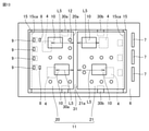
- FIG. 1 is a schematic plan view of the semiconductor device according to the first embodiment.
- FIG. 2 is a schematic cross-sectional view of the line segment II-II of FIG.
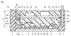
- FIG. 3 is a schematic cross-sectional view taken along the line segments III-III of FIG.
- the semiconductor device shown in FIGS. 1 to 3 mainly includes a base member 3, a semiconductor element 4, a case 6, a wiring board 11, a sealing member 14, and a terminal member 9.
- the base member 3 includes a heat dissipation layer 1, an insulating layer 25, and a conductor layer 24.
- the insulating layer 25 is laminated and arranged on the heat radiating layer 1 made of aluminum, copper, or the like.
- a conductor layer 24 as an upper electrode is arranged on the insulating layer 25.
- the upper surface of the conductor layer 24 constitutes the main surface 3a of the base member 3.
- the insulating layer 25 is formed so as to cover the upper surface of the heat radiating layer 1.
- the insulating layer 25 may be formed only on a part of the upper surface of the heat radiating layer 1 as long as it can insulate between the heat radiating layer 1 and the conductor layer 24.
- the conductor layer 24 is formed so as to cover a part of the upper surface of the insulating layer 25.
- the planar shape of the base member 3 is a quadrangular shape.
- the planar shape of the base member 3 may be a polygonal shape other than a quadrangular shape, or may be a circular shape.
- the material of the insulating layer 25 is not particularly limited, but may be a resin material in which at least one of fine particles and a filler is dispersed. At least one of fine particles and filler, such as alumina (Al 2 O 3), aluminum nitride (AlN), silicon nitride (Si 3 N 4), silicon dioxide (SiO 2), boron nitride (BN), diamond (C ), Silicon carbide (SiC) or boron oxide (B 2 O 3 ) may be formed of an inorganic ceramic material. At least one of the fine particles and the filler may be formed of a resin material such as a silicone resin or an acrylic resin.
- the resin material in which at least one of the fine particles and the filler is dispersed has an electrical insulating property.
- the resin material in which at least one of the fine particles and the filler is dispersed is not particularly limited, and may be an epoxy resin, a polyimide resin, a silicone resin, or an acrylic resin.
- the semiconductor element 4 is mounted on the main surface 3a, which is the upper surface of the conductor layer 24 of the base member 3.
- a plurality of semiconductor elements 4 are mounted on the main surface 3a of the base member 3.
- the semiconductor element 4 may be a power semiconductor element such as an insulated gate bipolar transistor (IGBT) or a metal oxide semiconductor field effect transistor (MOSFET), or may be a diode such as a freewheeling diode.
- the material constituting the semiconductor element 4 may be silicon (Si), or a wide bandgap semiconductor material such as silicon carbide (SiC), gallium nitride (GaN), or diamond.
- a required number of semiconductor elements 4 are fixed to the conductor layer 24 according to the application in which the semiconductor device is used.
- the plurality of semiconductor elements 4 may include the same type of semiconductor element 4 or may include different types of semiconductor elements 4. Regarding the materials constituting the plurality of semiconductor elements 4, the materials may be different for each semiconductor element 4 or may be the same.
- the semiconductor element 4 is bonded to the conductor layer 24 by a bonding material 2 made of solder or the like.
- a bonding material 2 made of solder or the like.
- any conductive material other than the above-mentioned solder can be used, but for example, silver or a silver alloy may be used.
- the case 6 is arranged so as to surround the outer periphery of the base member 3.
- the case 6 is connected to the outer peripheral portion of the base member 3.
- the case 6 surrounds the base member 3 and has a side wall 61 extending in a direction intersecting the main surface 3a of the base member 3.
- An opening is formed on the upper side of the side wall 61, which is located on the side opposite to the lower side connected to the base member 3.
- the size of the opening may be larger than the size of the base member 3.
- the planar shape of the opening may be the same as the planar shape of the base member 3.
- On the lower side of the side wall 61 a part of the case 6 is connected to the base member 3 so as to cover the outer peripheral portion of the base member 3.
- a part of the case 6 is connected to the outer peripheral portion of the insulating layer 25 of the base member 3. Further, a part of the case 6 is connected to the insulating layer 25 of the base member 3 and the outer peripheral end faces of the heat radiating layer 1.
- the case 6 and the base member 3 may be fixed by an adhesive or the like, but may be fixed by other means such as screws.
- a support portion 15 is formed on the inner peripheral surface 61a on the base member 3 side of the side wall 61.
- the support portion 15 is arranged at a distance from the semiconductor element 4 in a direction perpendicular to the main surface 3a of the base member 3.
- a support portion 15 is formed on each of a pair of side walls facing each other in the side wall 61.
- the support portion 15 is preferably formed so as to surround the semiconductor element 4 from at least two directions.
- the support portion 15 is formed so as to surround the semiconductor element 4 from three directions. More preferably, the support portion 15 is formed so as to surround the semiconductor element 4 from all directions.
- a resin having an electrically insulating property such as an epoxy resin, a polyimide resin, an acrylic resin, or a polyphenylene sulfide (PPS) resin may be used.
- the wiring board 11 is arranged at a position overlapping with the semiconductor element 4 when viewed from a direction perpendicular to the main surface 3a of the base member 3. That is, the wiring board 11 is arranged on the base member 3 at a distance from the semiconductor element 4.
- the electronic component 10 is mounted on the wiring board 11.
- the electronic components 10 are arranged on the surface 11a of the wiring board 11 located on the semiconductor element 4 side and the upper surface of the wiring board 11 located on the opposite side of the surface 11a. Further, the wiring board 11 is formed with a through hole 12 reaching the surface 11a from the upper surface.
- a plurality of the through holes 12 are formed on the wiring board 11.
- the diameter of the through hole 12 is, for example, 1 mm or less.
- the wiring board 11 is supported by the support portion 15 so that the surface 11a of the wiring board 11 is parallel to the main surface 3a of the base member 3.
- the size of the surface 11c on which the electronic component 10 is mounted on the wiring board 11 may be larger than the size of the conductor layer 24.
- the terminal member 9 is connected to the wiring board 11.
- the root portion of the terminal member 9 is connected to the outer peripheral portion of the wiring board 11.
- the terminal member 9 is preferably arranged at a position close to the side wall 61 of the case 6.
- the end portion 9a of the terminal member 9 is arranged so as to protrude from the upper surface of the sealing member 14.
- An internal connection terminal 8 is connected to the wiring board 11. As shown in FIGS. 1 and 3, the internal connection terminal 8 is connected to the wiring board 11 inside the terminal member 9 away from the side wall 61 of the case 6.
- the internal connection terminal 8 and the wiring board 11 are electrically connected by a bonding material such as solder. Further, the terminal member 9 and the wiring board 11 are also electrically connected by a bonding material such as solder.
- the joint material may be protected by covering the connection portion between the internal connection terminal 8 and the wiring board 11 and the connection portion between the terminal member 9 and the wiring board 11 with a resin.
- the lower end of the internal connection terminal 8 opposite to the upper end connected to the wiring board 11 is fixed to the case 6.
- the lower end portion of the internal connection terminal 8 is fixed to a portion of the case 6 that covers the outer peripheral portion of the base member 3.
- the wiring board 11 is supported by the case 6 by the outer peripheral portion of the surface 11a of the wiring board 11 coming into contact with the support portion 15.
- the support surface 15c which is the upper surface of the support portion 15, is in contact with the outer peripheral portion of the surface 11a of the wiring board 11.
- the support portion 15 arranged under the region to which the terminal member 9 is connected in the wiring board 11 includes the terminal member 9 and the extending portion extending from the inner peripheral surface 61a of the side wall 61 away from the outer peripheral portion of the wiring board 11. It includes a contact portion extending from the tip of the extending portion to the wiring board 11 side.
- the upper end surface of the contact portion is a support surface 15c.
- the support surface 15c is in contact with the surface 11a of the wiring board 11.
- the region of the wiring board 11 with which the support surface 15c of the support portion 15 contacts is the contact region 11aa. That is, at least a part of the support portion 15 comes into contact with the contact region 11aa located inside the outer peripheral end 11b of the wiring board 11 on the surface 11a located on the semiconductor element 4 side of the wiring board 11. In other words, the terminal member 9 is connected to the region on the outer peripheral end 11b side of the contact region 11aa on the wiring board 11. As a result, the terminal member 9 is in a state of being received by the support portion 15.
- the cross-sectional shape of the support portion 15 located directly below the terminal member 9 may be L-shaped as shown in FIG.
- the support portion 15 located below the terminal member 9 is formed with a concave portion 15b facing the region of the wiring board 11 to which the terminal member 9 is connected.
- the outer peripheral portion of the wiring board 11 to which the terminal member 9 is connected is partitioned from the region on the semiconductor element 4 side by the support portion 15.
- the support portion 15 is in contact with as many parts as possible on the outer peripheral portion of the wiring board 11.
- the support portion 15 may be formed on the entire circumference of the inner peripheral surface 61a of the side wall 61 of the case 6.
- the support portion 15 is preferably formed on at least two side walls 61 facing each other.
- the lower portion of the terminal member 9 penetrates the wiring board 11, but when the terminal member 9 is connected to the wiring board 11 without penetrating the wiring board 11, it is directly below the terminal member 9. It suffices if the support portion 15 is arranged.
- the support portion 15 may be in contact with the surface 11a of the wiring board 11 in a region located directly below the terminal member 9.
- a recess is formed in the support surface 15c of the support portion 15.
- the end portion of the terminal member 9 may be received in the recess.
- the case 6 in the semiconductor device shown in FIG. 3 includes a support portion 15 having an asymmetrical shape depending on the arrangement of the wiring board 11 and the terminal member 9, but the shape of the support portion 15 is symmetrical in FIG. It may have a simple shape.
- One of the semiconductor elements 4 is electrically connected to the internal connection terminal 8 by the conductive wire 5. Further, an external connection terminal 7 is embedded in the case 6. The lower portion of the external connection terminal 7 is exposed on the surface of the case 6 in the region overlapping with the base member 3. The upper part of the external connection terminal 7 protrudes from the top surface of the side wall 61 of the case 6. The conductor layer 24 to which the semiconductor element 4 is fixed and the lower portion of the external connection terminal 7 are connected by a conductive wire 5. The semiconductor element 4 is electrically connected to the external connection terminal 7 by the conductive wire 5.
- the material of the conductive wire 5 is not particularly limited, but a metal material such as copper or aluminum can be used.
- the sealing member 14 is arranged inside the case 6.
- the sealing member 14 seals the conductor layer 24 of the base member 3, the semiconductor element 4, the wiring board 11, the electronic component 10, the internal connection terminal 8, and the conductive wire 5.
- the sealing member 14 has an electrical insulating property and insulates between the sealed members.
- the thickness T1 of the sealing member 14 is large enough to allow both the semiconductor element 4 and the electronic component 10 mounted on the wiring board 11 to be embedded.
- the water vapor transmission rate of the materials constituting the wiring board 11 and the case 6 may be smaller than the water vapor transmission rate of the sealing member 14.
- the region where the semiconductor element 4 is arranged is surrounded by the wiring board 11 and the case 6, the possibility that moisture or the like reaches the semiconductor element 4 can be reduced.
- the contact portion between the support portion 15 and the wiring board 11 serves as a sealing portion, it is preferable that the support portion 15 is arranged so as to surround the region from at least two directions.
- the water vapor transmission rate is measured, for example, by the humidity sensor method specified in JIS standard K7126-1.
- an epoxy resin as the material of the sealing member 14, but the material is not limited to this, and for example, an insulating resin such as a silicone resin, a urethane resin, a polyimide resin, a polyamide resin or an acrylic resin can be used. You may use it.
- the material constituting the sealing member 14 may be an insulating resin material in which fine particles or fillers that improve the strength and thermal conductivity of the sealing member 14 are dispersed.
- the fine particles or fillers that improve the strength and thermal conductivity of the sealing member 14 include, for example, silicon dioxide (SiO 2 ), alumina (Al 2 O 3 ), aluminum nitride (AlN), boron nitride (BN), silicon nitride (BN). It may be formed of an inorganic ceramic material such as Si 3 N 4 ), diamond (C), silicon carbide (SiC) or boron oxide (B2O3).
- the process (S10) of preparing the members constituting the semiconductor device is carried out.
- members constituting the semiconductor device such as the base member 3, the semiconductor element 4, the case 6, the wiring board 11 on which the electronic component 10 is mounted, and the sealing member 14 are prepared.
- a step (S20) of joining the semiconductor element 4 to the base member 3 is performed.
- the solder and the semiconductor element 4 as the bonding material 2 are arranged on the base member 3.
- the semiconductor element 4 is joined to the base member 3 by melting the solder by reflow heating and then solidifying it.
- a step (S30) of joining the case 6 to the base member 3 is performed.
- the adhesive (not shown) is uniformly applied to the outer peripheral portion of the base member 3 to which the semiconductor element 4 is soldered.
- the case 6 is brought into contact with the portion to which the adhesive is applied, and the case 6 and the base member 3 are adhered to each other.
- the case 6 includes an external connection terminal 7 and an internal connection terminal 8 as shown in FIGS. 1 and 3.
- the external connection terminal 7 passes through the case 6 and is led out to the outside of the semiconductor device.
- the internal connection terminal 8 is arranged so as to extend upward (along the side wall 61) from the lower part of the case 6 as shown in FIG.
- step (S40) a circuit is formed by electrically connecting the semiconductor element 4, the conductor layer 24 of the base member 3, the external connection terminal 7, the internal connection terminal 8, and the like using the conductive wire 5. ..
- the step (S50) of arranging the wiring board 11 is carried out.
- the wiring board 11 is placed in the case 6 so that the support surface 15c of the support portion 15 formed on the side wall 61 of the case 6 and the outer peripheral portion of the lower surface 11a of the wiring board 11 come into contact with each other. Place it inside.
- the wiring board 11 is arranged at a position where the wiring board 11 and the tip of the internal connection terminal 8 can be joined. At this time, it is preferable that the contact area between the support surface 15c and the wiring board 11 is as large as possible. It is preferable to make contact with the support surface 15c on the entire circumference of the outer peripheral portion of the wiring board 11. It is preferable that the support surface 15c and the wiring board 11 come into contact with each other at least on two opposite sides of the outer peripheral portion of the wiring board 11 as shown in FIGS. 1 and 3.
- soldering process (S60) is carried out.
- the lower portion of the terminal member 9 for external connection is arranged at a position where it is joined to the wiring board 11. Then, the wiring board 11 and the internal connection terminal 8 are electrically connected by soldering. Further, the wiring board 11 and the terminal member 9 are electrically connected by soldering.
- the sealing step (S70) is carried out.
- the sealing resin as the sealing member 14 is injected into the region under the wiring board 11 from the portion where the wiring board 11 is not supported by the support portion 15. Further, the sealing member 14 is injected into the case 6 so as to embed all the electronic components 10 of the wiring board 11.
- the sealing member 14 includes a bonding material 2 such as solder, a conductor layer 24, a semiconductor element 4, a conductive wire 5, an internal connection terminal 8, an electronic component 10, a wiring board 11, and a case.
- the support portion 15 formed on the inner peripheral surface 61a of the side wall 61 of 6 and the connection portion between the support portion 15 and the wiring board 11 are arranged so as to be embedded. As a result, the semiconductor devices shown in FIGS. 1 to 3 can be obtained.
- a semiconductor device includes a base member 3, a semiconductor element 4, a case 6, a wiring board 11, a sealing member 14, and a terminal member 9.
- the base member 3 has a main surface 3a.
- the semiconductor element 4 is mounted on the main surface 3a of the base member 3.
- the case 6 has a side wall 61 that surrounds the base member 3.
- a support portion 15 is formed on the inner peripheral surface 61a on the side of the base member 3 on the side wall 61.
- the wiring board 11 is arranged at a position overlapping with the semiconductor element 4 when viewed from a direction perpendicular to the main surface 3a of the base member 3.
- the electronic component 10 is mounted on the wiring board 11.
- the sealing member 14 is arranged inside the case 6.
- the sealing member 14 seals the semiconductor element 4 and the wiring board 11.
- the terminal member 9 is connected to a region on the outer peripheral end 11b side of the contact region 11aa on the wiring board 11.
- the terminal member 9 includes an end portion 9a protruding from the surface of the sealing member 14.
- the semiconductor element 4 is seen from the surface of the sealing member 14 as compared with the case where the wiring board 11 does not exist. It is possible to lengthen the path length for substances such as water and sulfur gas to enter from the outside. Further, since the terminal member 9 is connected to the outer peripheral side of the contact region 11aa where the support portion 15 contacts in the wiring board 11, the terminal member 9 seems to extend from the vicinity of the semiconductor element 4 to the outside of the sealing member 14. Therefore, it is possible to reduce the possibility that a substance such as moisture reaches the semiconductor element 4 from the outside through the contact interface between the terminal member 9 and the sealing member 14.
- the contact interface between the wiring board 11 and the support portion 15 and the sealing member 14 is formed. It is formed.
- the contact interface traps a substance such as water that has reached the outer peripheral portion of the wiring board 11, and as a result, the possibility that the substance such as water reaches the semiconductor element 4 can be reduced. As a result, the reliability of the semiconductor device can be improved.
- the water vapor transmission rate of the materials constituting the wiring board 11 and the case 6 may be smaller than the water vapor transmission rate of the sealing member 14.
- the wiring substrate 11 having a relatively low water vapor permeability is embedded in the semiconductor element 4 inside the sealing member 14, the upper surface of the sealing member 14 is directed toward the semiconductor element 4.
- the wiring substrate 11 acts as a member that prevents the infiltration of the water or a member that lengthens the intrusion path length of the water. Therefore, the possibility that a substance such as water reaches the semiconductor element 4 can be reduced.
- the base member 3 may include a conductor layer 24 to which the semiconductor element 4 is connected.
- the size of the surface 11c on which the electronic component 10 is mounted on the wiring board 11 may be larger than the size of the conductor layer 24.
- the wiring board 11 arranged in the sealing member 14 can sufficiently lengthen the intrusion path length of a substance such as water from the upper surface of the sealing member 14.
- the support portion 15 may include a concave portion 15b facing a region to which the terminal member 9 is connected in the wiring board 11.
- the concave portion 15b of the support portion 15 can form a seal portion that surrounds the region to which the terminal member 9 is connected in the wiring board 11. Therefore, the sealing portion can prevent substances such as water from entering the semiconductor element 4 side through the bonding interface between the terminal member 9 and the sealing member 14.
- the base member 3 may include a heat dissipation layer 1.
- the material constituting the heat radiating layer 1 may be metal.
- the base member 3 may include a conductor layer 24 and a heat radiating layer 1.
- the semiconductor element 4 is connected to the conductor layer 24.
- the heat radiating layer 1 is connected to the conductor layer 24 via the insulating layer 25.
- the material constituting the heat radiating layer 1 may be metal.
- the configuration of the semiconductor device can be simplified as compared with the case where the heat radiation layer is connected to the base member 3 as a separate member.
- the support portion 15 may be in contact with the wiring board 11 in at least two directions of the outer peripheral portion of the wiring board 11.
- the contact portion between the support portion 15 and the wiring board 11 acts as a sealing portion, and the possibility that a substance such as water invades the semiconductor element 4 from the upper surface of the sealing member 14 can be reduced.
- components such as electronic components 10 are not exposed on the upper surface of the sealing member 14 inside the support surface end portion 15ca located on the distal end side of the support portion 15. Is preferable.
- the connection interface between the electronic component 10 and the sealing member 14 is not exposed on the upper surface of the sealing member 14 inside the support surface end portion 15ca. Therefore, it is possible to suppress the occurrence of problems such as atmospheric gas such as water vapor and sulfur gas invading the inside of the semiconductor device through the connection interface.
- the wiring board 11 inside the sealing member 14 and above the semiconductor element 4 the intrusion path length of the gas that can be formed from the upper surface of the sealing member 14 to the semiconductor element 4 is lengthened. Can be done. As a result, it is possible to reduce the possibility that moisture or the like reaches the semiconductor element 4 and cause a defect without requiring a special additional member, and a highly reliable semiconductor device can be obtained.
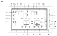
- FIG. 4 is a schematic plan view showing a modified example of the semiconductor device according to the first embodiment.
- FIG. 4 corresponds to FIG.
- the semiconductor device shown in FIG. 4 basically has the same configuration as the semiconductor device shown in FIGS. 1 to 3, but the configuration of the support portion 15 is different from that of the semiconductor device shown in FIGS. 1 to 3. There is. Specifically, in the semiconductor device shown in FIG. 4, a notch portion 15a in which a part of the support portion 15 is missing is formed.
- the distance L1 from the notch portion 15a to the semiconductor element 4 is preferably larger than the thickness T1 of the sealing member 14.
- the sealing member 14 when the sealing member 14 is supplied to the inside of the case 6 in the method of manufacturing a semiconductor device, the sealing member 14 can be supplied to the region between the wiring board 11 and the semiconductor element 4 via the notch portion 15a. Further, the distance L1 from the notch portion 15a to the semiconductor element 4 in a plan view (when viewed from a direction perpendicular to the main surface 3a of the base member 3) is from the thickness T1 of the sealing member 14 (see FIG. 1). Since it is large, it is possible to suppress an increase in the possibility that a substance such as water invades the semiconductor element 4 from the upper surface of the sealing member 14 due to the formation of the notch portion 15a.
- FIG. 5 is a schematic plan view of the semiconductor device according to the second embodiment.
- FIG. 6 is a schematic plan view showing the positional relationship between the sealing member injection port and the insulating member in the semiconductor device shown in FIG.
- FIG. 6 schematically shows the arrangement of the base member 3, the semiconductor element 4, and the conductive wire 5 located under the wiring board 11 in FIG.
- FIG. 7 is a schematic cross-sectional view of the line segment VII-VII of FIG.
- FIG. 5 corresponds to FIG. 1
- FIG. 7 corresponds to FIG.
- the semiconductor device shown in FIGS. 5 to 7 basically has the same configuration as the semiconductor device shown in FIGS. 1 to 3, but the wiring board 11 is formed with a sealing member injection port 13. , And the configuration of the support portion 15 are different from the semiconductor devices shown in FIGS. 1 to 3.
- the hole that penetrates from the back surface 11a on the back surface of the wiring board 11 to the upper surface, does not insert an electronic component, and has a diameter of 1 mm or more is used as the sealing member injection port 13.
- the sealing member injection port 13 is formed at a position overlapping the case 6.
- the sealing member injection port 13 in the wiring board 11 is formed at a position overlapping the case surface 6a, which is the upper surface of the portion extending on the outer peripheral portion of the base member 3 in the case 6. There is. That is, in a plan view, the sealing member injection port 13 is arranged at a position that does not overlap with the conductor layer 24 of the base member 3.
- the sealing member injection port 13 is located at the farthest point from the conductor layer 24, but in the plan view shown in FIG. 6, at least between the sealing member injection port 13 and the conductor layer 24. It is preferable that the distance L2 is equal to or larger than the thickness T1 (see FIG. 1) of the sealing member 14. As described above, the sealing member injection port 13 is installed at a position where there is no sealing member injection port 13 on the conductor layer 24 and the sealing member injection port 13 is at least separated from the conductor layer 24 by a thickness T1 or more of the sealing member 14. , It is possible to prevent gas such as water vapor or sulfur gas from reaching the semiconductor element 4 from the upper surface of the sealing member 14.
- the sealing member injection port 13 is formed in the wiring board 11
- the sealing member 14 can be injected from the sealing member injection port 13 to the lower side of the wiring board 11. Therefore, the support portion 15 is formed so as to surround the entire circumference of the wiring board 11 so as to be in contact with the entire outer circumference of the wiring board 11. That is, the support portion 15 is formed in an annular shape in a plan view so as to orbit the inner peripheral surface of the side wall of the case 6.
- the method for manufacturing the semiconductor device shown in FIGS. 5 to 7 is basically the same as the method for manufacturing the semiconductor device shown in FIGS. 1 to 3, but the configuration of the wiring board 11 and the sealing step (S70).
- the content is different from the manufacturing method of the semiconductor device shown in FIGS. 1 to 3.
- the sealing member injection port 13 is formed on the wiring board 11 prepared in the preparation step (S10).
- the sealing member injection port 13 may be formed at the end of the wiring board 11.
- the steps (S20) to (S60) in the method for manufacturing the semiconductor device shown in FIGS. 1 to 3 are carried out.
- a resin material or the like as a sealing member is injected into the lower side of the wiring board 11 via the sealing member injection port 13. In this way, the semiconductor devices shown in FIGS. 5 to 7 can be obtained.
- the sealing member injection port 13 may be formed on the wiring board 11.
- the sealing member injection port 13 may be formed at a position overlapping the case 6 when viewed from a direction perpendicular to the main surface 3a of the base member 3.
- the sealing member 14 can be easily injected under the wiring board 11 via the sealing member injection port 13. Further, by setting the distance L2 between the conductor layer 24 constituting the base member 3 and the sealing member injection port 13 to be larger than the thickness T1 of the sealing member 14, the sealing member injection port 13 is used. It is possible to prevent substances such as moisture and gas from reaching the conductor layer 24 and the semiconductor element 4 from the upper surface of the sealing member 14.
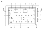
- FIG. 8 is a schematic plan view of the semiconductor device according to the third embodiment.
- FIG. 9 is a schematic plan view showing the positional relationship between the sealing member injection port and the semiconductor element in the semiconductor device shown in FIG. 8 corresponds to FIG. 5, and FIG. 9 corresponds to FIG.
- the semiconductor device shown in FIGS. 8 and 9 basically has the same configuration as the semiconductor device shown in FIGS. 5 to 7, but the position of the sealing member injection port 13 in the wiring board 11 is different. .. Specifically, the sealing member injection port 13 is formed in the central portion of the wiring board 11. In the plan view shown in FIGS. 8 and 9 (when viewed from a direction perpendicular to the main surface 3a of the base member 3), the sealing member injection port 13 is arranged in a region that does not overlap with the semiconductor element 4.
- the sealing member injection port 13 is located at the farthest point from the semiconductor element 4, but in the plan view shown in FIG. 9, at least the distance L3 between the sealing member injection port 13 and the semiconductor element 4 is L3.
- the thickness of the sealing member 14 is T1 or more (see FIG. 1).
- the sealing member injection port 13 is not provided on the semiconductor element 4, and the sealing member injection port 13 is installed at a position at least separated from the semiconductor element 4 by at least the thickness T1 of the sealing member 14 to seal the semiconductor element 4. It is possible to prevent gas such as water vapor or sulfur gas from reaching the semiconductor element 4 from the upper surface of the stopping member 14 via the sealing member injection port 13.
- the method for manufacturing the semiconductor device shown in FIGS. 8 and 9 is basically the same as the method for manufacturing the semiconductor device shown in FIGS. 1 to 3, but the configuration of the wiring board 11 and the sealing step (S70).
- the content is different from the manufacturing method of the semiconductor device shown in FIGS. 1 to 3.
- a sealing member injection port 13 is formed in the central portion of the wiring board 11 prepared in the preparation step (S10).
- the steps (S20) to (S60) in the method for manufacturing the semiconductor device shown in FIGS. 1 to 3 are carried out.
- a resin material or the like as a sealing member is injected into the lower side of the wiring board 11 via the sealing member injection port 13. In this way, the semiconductor devices shown in FIGS. 8 and 9 can be obtained.
- the sealing member injection port 13 may be formed on the wiring board 11.
- the sealing member injection port 13 may be formed at a position that does not overlap with the semiconductor element 4 when viewed from a direction perpendicular to the main surface 3a of the base member 3.
- the sealing member 14 can be easily injected under the wiring board 11 via the sealing member injection port 13. Further, by setting the distance L3 between the semiconductor element 4 and the sealing member injection port 13 to be larger than the thickness T1 of the sealing member 14, the upper surface of the sealing member 14 is passed through the sealing member injection port 13. It is possible to prevent substances such as moisture and gas from reaching the semiconductor element 4.
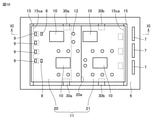
- FIG. 10 is a schematic plan view of the semiconductor device according to the fourth embodiment.
- FIG. 11 is a schematic cross-sectional view of the line segment XI-XI of FIG. 10 corresponds to FIG. 1 and FIG. 11 corresponds to FIG.
- the semiconductor device shown in FIGS. 10 and 11 basically has the same configuration as the semiconductor device shown in FIGS. 1 to 3, but the configuration of the wiring board 11 and the configurations of the support portions 15, 30a and 30b are different. It is different from the semiconductor device shown in FIGS. 1 to 3. That is, in the semiconductor device shown in FIGS. 10 and 11, the wiring board 11 is composed of two boards, a first board 20 and a second board 21. When the wiring board 11 is composed of a plurality of boards, the number of the boards may be three or more.
- the side wall of the case 6 is formed with a support portion 15 and additional support portions 30a and 30b protruding in a direction intersecting the direction of protrusion from the side wall surface of the support portion 15.
- the first substrate 20 is supported by the support portion 15 on the left side of FIG. 10 and the additional support portion 30a.
- the heights of the support portion 15 in contact with the first substrate 20 and the additional support portion 30a in the direction perpendicular to the main surface 3a of the base member 3 are substantially the same.
- the second substrate 21 is supported by the support portion 15 on the right side of FIG. 10 and the additional support portion 30b.
- the heights of the support portion 15 in contact with the second substrate 21 and the additional support portion 30b in the direction perpendicular to the main surface 3a of the base member 3 are substantially the same.
- the additional support portion 30a is arranged at a position away from the base member 3 from the additional support portion 30b in the direction perpendicular to the main surface 3a of the base member 3.
- the end portion 20a of the first substrate 20 is arranged on the second substrate 21 at a distance L4.
- a part of the first substrate 20 and a part of the second substrate 21 overlap each other when viewed from a direction perpendicular to the main surface 3a of the base member 3.
- the distance L4 may be smaller than the width of the overlapping portion between the first substrate 20 and the second substrate 21 in the plan view shown in FIG. 10 (when viewed from a direction perpendicular to the main surface 3a of the base member 3). preferable.
- the plane shape of the first substrate 20 and the second substrate 21 is a quadrangular shape, respectively.
- the direction along the main surface 3a of the base member 3 from the first substrate 20 to the second substrate 21 is the first direction, and the direction perpendicular to the first direction and along the main surface 3a is the first direction.
- the width in the first direction may be smaller or larger than the width in the second direction.
- the width in the first direction may be smaller or larger than the width in the second direction.
- the method for manufacturing the semiconductor device shown in FIGS. 10 and 11 is basically the same as the method for manufacturing the semiconductor device shown in FIGS. 1 to 3, but the configuration of the wiring board 11, the configuration of the case 6, and the wiring are the same.
- the content of the step (S50) for arranging the substrate 11 is different from the method for manufacturing the semiconductor device shown in FIGS. 1 to 3.
- the wiring board 11 prepared in the preparation step (S10) is two boards, the first board 20 and the second board 21. Further, in addition to the support portion 15, additional support portions 30a and 30b are formed on the side wall of the case 6. After that, the steps (S20) to (S40) in the method for manufacturing the semiconductor device shown in FIGS. 1 to 3 are carried out.
- the second substrate 21 is arranged inside the case 6 so that the outer peripheral portion of the second substrate 21 comes into contact with the support portion 15 and the additional support portion 30b. ..
- the first substrate 20 is arranged inside the case 6 so that the outer peripheral portion of the first substrate 20 comes into contact with the support portion 15 and the additional support portion 30a.
- a part of the first substrate 20 on the end portion 20a side is arranged so as to overlap the second substrate 21.
- the first substrate 20 and the second substrate 21 do not come into contact with each other and are arranged at a distance L4.
- the wiring board 11 may include a first board 20 and a second board 21.
- a part of the first substrate 20 and a part of the second substrate 21 may overlap when viewed from a direction perpendicular to the main surface 3a of the base member 3.
- the distance L4 between the first substrate 20 and the second substrate 21 in the overlapping region is the plan view (when viewed from a direction perpendicular to the main surface 3a of the base member 3) shown in FIG. It is preferably smaller than the width of the overlapping portion between the first substrate 20 and the second substrate 21.
- the semiconductor element is formed from the upper surface of the sealing member 14 via the overlapping portion between the first substrate 20 and the second substrate 21. It is possible to reduce the possibility that substances such as water and gas reach 4.
- FIG. 12 is a schematic cross-sectional view showing a first modification of the semiconductor device according to the fourth embodiment.
- FIG. 12 corresponds to FIG.
- the semiconductor device shown in FIG. 12 basically has the same configuration as the semiconductor device shown in FIGS. 10 and 11, but the first substrate 20 and the second substrate 21 are in contact with each other in an overlapping region. It is different from the semiconductor device shown in FIGS. 10 and 11.
- the same effect as that of the semiconductor device shown in FIGS. 10 and 11 can be obtained.
- the semiconductor device shown in FIG. 12 since the first substrate 20 and the second substrate 21 are in contact with each other, moisture, gas, or the like may be applied to the semiconductor element 4 from the upper surface of the sealing member 14 through the overlapped region. The possibility of the substance reaching can be reduced.
- FIG. 13 is a schematic plan view showing a second modification of the semiconductor device according to the fourth embodiment.
- the semiconductor device shown in FIG. 13 basically has the same configuration as the semiconductor device shown in FIGS. 10 and 11, but the first substrate 20 and the second substrate 21 do not overlap each other in a plan view and are spaced apart from each other. It is different from the semiconductor devices shown in FIGS. 10 and 11 in that they are arranged so as to be separated from each other.
- the first substrate 20 and the second substrate 21 are arranged at a distance from each other when viewed from a direction perpendicular to the main surface 3a of the base member 3.
- the end portion 20a of the first substrate 20 and the end portion 21a of the second substrate 21 face each other with a gap.
- the semiconductor element 4 is arranged at a position that does not overlap with the gap 31 between the first substrate 20 and the second substrate 21.
- the distance L5 between the gap 31 and the semiconductor element 4 as viewed from the above direction is preferably larger than the thickness T1 (see FIG. 1) of the sealing member 14 in the above direction.
- the wiring board 11 may include the first board 20 and the second board 21.
- the first substrate 20 and the second substrate 21 may be arranged at a distance from each other when viewed from a direction perpendicular to the main surface 3a of the base member 3.
- the semiconductor element 4 may be arranged at a position that does not overlap with the gap 31 between the first substrate 20 and the second substrate 21.
- the distance L5 between the gap 31 and the semiconductor element 4 as seen from the above direction may be larger than the thickness T1 of the sealing member 14 in the above direction.
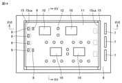
- FIG. 14 is a schematic plan view of the semiconductor device according to the fifth embodiment.
- FIG. 15 is a schematic cross-sectional view of the line segment XV-XV of FIG.
- FIG. 16 is a schematic cross-sectional view of the line segment XVI-XVI of FIG. 14 to 16 correspond to FIGS. 1 to 3, respectively.
- the semiconductor device shown in FIGS. 14 to 16 basically has the same configuration as the semiconductor device shown in FIGS. 1 to 3, but has a configuration of the base member 3 and a heat dissipation layer as a separate member from the base member 3. It is different from the semiconductor device shown in FIGS. 1 to 3 in that the case 6 and the base member 3 are connected to each other via the heat radiation layer 1.
- the base member 3 is composed of an insulating layer made of an inorganic ceramic material and a conductor layer connected to the upper surface and the lower surface of the insulating layer.
- the inorganic ceramic material for example, alumina (Al 2 O 3 ), aluminum nitride (AlN), silicon nitride (Si 3 N 4 ), silicon dioxide (SiO 2 ), boron nitride (BN) or the like can be used.
- the size of the base member 3 is smaller than the size of the wiring board 11.
- the heat radiating layer 1 is connected to the conductor layer constituting the lower surface of the base member 3 via a bonding material 2 such as solder.
- a case 6 is connected to the outer peripheral portion of the heat radiating layer 1 via an adhesive (not shown).
- the manufacturing method of the semiconductor device shown in FIGS. 14 to 16 is basically the same as the manufacturing method of the semiconductor device shown in FIGS. 1 to 3, but the configuration of the base member 3 and the heat dissipation layer 1 and the case 6 are described.
- the content of the step (S30) of joining to the base member 3 is different from the manufacturing method of the semiconductor device shown in FIGS. 1 to 3.
- the base member 3 prepared in the preparation step (S10) a laminate in which an insulating layer made of the above-mentioned inorganic ceramic material and two conductor layers are laminated is prepared. Further, the heat radiating layer 1 is connected to the base member 3 via the bonding material 2.
- step (S20) in the method for manufacturing the semiconductor device shown in FIGS. 1 to 3 is carried out.
- step (S30) in the step (S30) is joined to the outer peripheral portion of the heat radiation layer 1 with an adhesive.
- steps (S40) to (S70) in the method for manufacturing the semiconductor device shown in FIGS. 1 to 3 are carried out. In this way, the semiconductor devices shown in FIGS. 14 to 16 can be obtained.
- the semiconductor device shown in FIGS. 14 to 16 may include a heat dissipation layer 1 connected to the base member 3.
- the same effect as that of the semiconductor device shown in FIGS. 1 to 3 can be obtained, and since the heat dissipation layer 1 and the base member 3 are prepared as separate members, the degree of freedom in selecting the configuration of the semiconductor device is increased. Can be made larger.
- Embodiment 6 the semiconductor device according to the first to fifth embodiments described above is applied to a power conversion device.
- the present disclosure is not limited to a specific power conversion device, the case where the present disclosure is applied to a three-phase inverter will be described below as the sixth embodiment.
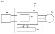
- FIG. 17 is a block diagram showing a configuration of a power conversion system to which the power conversion device according to the present embodiment is applied.
- the power conversion system shown in FIG. 17 is composed of a power supply 100, a power conversion device 200, and a load 300.
- the power supply 100 is a DC power supply, and supplies DC power to the power conversion device 200.
- the power supply 100 can be configured with various things, for example, it can be configured with a DC system, a solar cell, a storage battery, or it can be configured with a rectifier circuit or an AC / DC converter connected to an AC system. May be good.
- the power supply 100 may be configured by a DC / DC converter that converts the DC power output from the DC system into a predetermined power.
- the power conversion device 200 is a three-phase inverter connected between the power supply 100 and the load 300, converts the DC power supplied from the power supply 100 into AC power, and supplies AC power to the load 300. As shown in FIG. 17, the power conversion device 200 has a main conversion circuit 201 that converts DC power into AC power and outputs it, and a control circuit 203 that outputs a control signal for controlling the main conversion circuit 201 to the main conversion circuit 201. And have.
- the load 300 is a three-phase electric motor driven by AC power supplied from the power conversion device 200.
- the load 300 is not limited to a specific application, and is an electric motor mounted on various electric devices.
- the load 300 is used as an electric motor for a hybrid vehicle, an electric vehicle, a railroad vehicle, an elevator, or an air conditioner.
- the main conversion circuit 201 includes a switching element and a freewheeling diode (not shown), and by switching the switching element, the DC power supplied from the power supply 100 is converted into AC power and supplied to the load 300.
- the main conversion circuit 201 is a two-level three-phase full bridge circuit, and has six switching elements and each switching element. It can consist of six anti-parallel freewheeling diodes.
- each switching element and each freewheeling diode of the main conversion circuit 201 is a switching element or a freewheeling diode included in the semiconductor device 202 corresponding to the semiconductor device according to any one of the above-described first to fifth embodiments. ..
- the six switching elements are connected in series for each of the two switching elements to form an upper and lower arm, and each upper and lower arm constitutes each phase (U phase, V phase, W phase) of the full bridge circuit. Then, the output terminals of each upper and lower arm, that is, the three output terminals of the main conversion circuit 201 are connected to the load 300.
- the main conversion circuit 201 includes a drive circuit (not shown) for driving each switching element
- the drive circuit may be built in the semiconductor device 202, or the drive circuit may be provided separately from the semiconductor device 202. It may be provided.
- the drive circuit generates a drive signal for driving the switching element of the main conversion circuit 201 and supplies it to the control electrode of the switching element of the main conversion circuit 201.
- a drive signal for turning on the switching element and a drive signal for turning off the switching element are output to the control electrode of each switching element.
- the drive signal When the switching element is kept on, the drive signal is a voltage signal (on signal) equal to or higher than the threshold voltage of the switching element, and when the switching element is kept off, the drive signal is a voltage equal to or lower than the threshold voltage of the switching element. It becomes a signal (off signal).
- the control circuit 203 controls the switching element of the main conversion circuit 201 so that the desired power is supplied to the load 300. Specifically, the time (on time) in which each switching element of the main conversion circuit 201 should be in the on state is calculated based on the electric power to be supplied to the load 300.
- the main conversion circuit 201 can be controlled by PWM control that modulates the on-time of the switching element according to the voltage to be output. Then, a control command (control signal) is output to the drive circuit provided in the main conversion circuit 201 so that an on signal is output to the switching element that should be turned on at each time point and an off signal is output to the switching element that should be turned off. Is output.
- the drive circuit outputs an on signal or an off signal as a drive signal to the control electrode of each switching element according to this control signal.
- the semiconductor device according to any one of the first to fifth embodiments is applied as the semiconductor device 202 constituting the main conversion circuit 201, so that the reliability can be improved. can.
- the present disclosure is not limited to this, and can be applied to various power conversion devices.
- a two-level power conversion device is used, but a three-level or multi-level power conversion device may be used, and when power is supplied to a single-phase load, the present disclosure is disclosed to a single-phase inverter. You may apply it.
- the present disclosure can be applied to a DC / DC converter or an AC / DC converter.
- the power conversion device to which the present disclosure is applied is not limited to the case where the above-mentioned load is an electric motor, and is, for example, a power supply device of a discharge machine, a laser machine, an induction heating cooker, or a non-contact power supply system. It can also be used as a power conditioner for a photovoltaic power generation system, a power storage system, or the like.
Landscapes
- Engineering & Computer Science (AREA)
- Microelectronics & Electronic Packaging (AREA)
- Power Engineering (AREA)
- Structures Or Materials For Encapsulating Or Coating Semiconductor Devices Or Solid State Devices (AREA)
- Chemical & Material Sciences (AREA)
- Ceramic Engineering (AREA)
Abstract
Description
<半導体装置の構成>
図1は、実施の形態1に係る半導体装置の平面模式図である。図2は、図1の線分II-IIにおける断面模式図である。図3は、図1の線分III-IIIにおける断面模式図である。図1から図3に示す半導体装置は、ベース部材3と、半導体素子4と、ケース6と、配線基板11と、封止部材14と、端子部材9とを主に備える。
図1から図3に示した半導体装置の製造方法を説明する。
本開示に従った半導体装置は、ベース部材3と、半導体素子4と、ケース6と、配線基板11と、封止部材14と、端子部材9とを備える。ベース部材3は主面3aを有する。半導体素子4は、ベース部材3の主面3a上に搭載される。ケース6は、ベース部材3を囲む側壁61を有する。側壁61においてベース部材3側の内周面61aには支持部15が形成される。配線基板11は、ベース部材3の主面3aに対して垂直な方向から見て、半導体素子4と重なる位置に配置される。配線基板11には電子部品10が搭載される。支持部15の少なくとも一部は、配線基板11の半導体素子4側に位置する面11aにおいて、配線基板11の外周端11bより内側に位置する接触領域11aaに接触する。封止部材14は、ケース6の内部に配置される。封止部材14は、半導体素子4と配線基板11とを封止する。端子部材9は、配線基板11において、接触領域11aaより外周端11b側の領域に接続される。端子部材9は、封止部材14の表面から突出する端部9aを含む。
図4は、実施の形態1に係る半導体装置の変形例を示す平面模式図である。図4は図1に対応する。図4に示した半導体装置は、基本的には図1から図3に示した半導体装置と同様の構成を備えるが、支持部15の構成が図1から図3に示した半導体装置と異なっている。具体的には、図4に示した半導体装置では、支持部15の一部が欠けている切欠き部15aが形成されている。切欠き部15aから半導体素子4までの距離L1は、好ましくは封止部材14の厚みT1より大きい。
<半導体装置の構成>
図5は、実施の形態2に係る半導体装置の平面模式図である。図6は、図5に示した半導体装置における封止部材注入口と絶縁部材との位置関係を示す平面模式図である。図6は、図5において配線基板11下に位置するベース部材3と半導体素子4と導電ワイヤ5との配置を模式的に示している。図7は、図5の線分VII-VIIにおける断面模式図である。図5は図1に対応し、図7は図3に対応する。
図5から図7に示した半導体装置の製造方法は、基本的には図1から図3示した半導体装置の製造方法と同様であるが、配線基板11の構成および封止工程(S70)の内容が図1から図3に示した半導体装置の製造方法と異なっている。具体的には、準備する工程(S10)において準備される配線基板11には、封止部材注入口13が形成されている。配線基板11の端部に封止部材注入口13が形成されていてもよい。その後、図1から図3に示した半導体装置の製造方法における工程(S20)から工程(S60)を実施する。そして、封止工程(S70)において、封止部材注入口13を介して配線基板11の下側に封止部材としての樹脂材料などを注入する。このようにして、図5から図7に示した半導体装置を得ることができる。
上記半導体装置において、配線基板11には封止部材注入口13が形成されてもよい。ベース部材3の主面3aに対して垂直な方向から見て、封止部材注入口13は、ケース6と重なる位置に形成されていてもよい。
<半導体装置の構成>
図8は、実施の形態3に係る半導体装置の平面模式図である。図9は、図8に示した半導体装置における封止部材注入口と半導体素子との位置関係を示す平面模式図である。図8は図5に対応し、図9は図6に対応する。図8および図9に示した半導体装置は、基本的には図5から図7に示した半導体装置と同様の構成を備えるが、配線基板11における封止部材注入口13に位置が異なっている。具体的には、配線基板11の中央部に封止部材注入口13が形成されている。図8および図9に示す平面視(ベース部材3の主面3aに対して垂直な方向から見た場合)において、封止部材注入口13は半導体素子4と重ならない領域に配置されている。
図8および図9に示した半導体装置の製造方法は、基本的には図1から図3示した半導体装置の製造方法と同様であるが、配線基板11の構成および封止工程(S70)の内容が図1から図3に示した半導体装置の製造方法と異なっている。具体的には、準備する工程(S10)において準備される配線基板11の中央部には、封止部材注入口13が形成されている。その後、図1から図3に示した半導体装置の製造方法における工程(S20)から工程(S60)を実施する。そして、封止工程(S70)において、封止部材注入口13を介して配線基板11の下側に封止部材としての樹脂材料などを注入する。このようにして、図8および図9に示した半導体装置を得ることができる。
上記半導体装置において、配線基板11には封止部材注入口13が形成されてもよい。ベース部材3の主面3aに対して垂直な方向から見て、封止部材注入口13は、半導体素子4と重ならない位置に形成されていてもよい。
<半導体装置の構成>
図10は、実施の形態4に係る半導体装置の平面模式図である。図11は、図10の線分XI-XIにおける断面模式図である。図10は図1に対応し、図11は図3に対応する。図10および図11に示した半導体装置は、基本的には図1から図3に示した半導体装置と同様の構成を備えるが、配線基板11の構成および支持部15,30a,30bの構成が図1から図3に示した半導体装置と異なっている。すなわち、図10および図11に示した半導体装置では、配線基板11が第1基板20と第2基板21との2枚の基板によって構成されている。配線基板11を複数枚の基板により構成する場合、当該基板の枚数を3枚以上としてもよい。
図10および図11に示した半導体装置の製造方法は、基本的には図1から図3示した半導体装置の製造方法と同様であるが、配線基板11の構成およびケース6の構成と、配線基板11を配置する工程(S50)の内容が図1から図3に示した半導体装置の製造方法と異なっている。具体的には、準備する工程(S10)において準備される配線基板11が第1基板20と第2基板21という2枚の基板である。また、ケース6の側壁には支持部15に加えて追加の支持部30a、30bが形成されている。その後、図1から図3に示した半導体装置の製造方法における工程(S20)から工程(S40)を実施する。そして、配線基板11を配置する工程(S50)において、まず第2基板21の外周部が支持部15と追加の支持部30bとに接触するように、ケース6内部に第2基板21を配置する。次に、第1基板20の外周部が支持部15と追加の支持部30aとに接触するように、ケース6内部に第1基板20を配置する。このとき、第1基板20の端部20a側の一部が第2基板21上に重なるように配置される。第1基板20と第2基板21とは接触せず、距離L4を隔てて配置される。その後、図1から図3に示した半導体装置の製造方法における工程(S60)および工程(S70)を実施することで、図10および図11に示した半導体装置を得ることができる。
上記半導体装置において、配線基板11は、第1基板20と、第2基板21とを含んでいてもよい。ベース部材3の主面3aに対して垂直な方向から見て、第1基板20の一部と第2基板21の一部とは重なっていてもよい。互いに重なっている領域における第1基板20と第2基板21との間の距離L4は、図10に示す平面視(ベース部材3の主面3aに対して垂直な方向から見た場合)での第1基板20と第2基板21との重なり部分の幅より小さいことが好ましい。
図12は、実施の形態4に係る半導体装置の第1変形例を示す断面模式図である。図12は図11に対応する。図12に示した半導体装置は、基本的には図10および図11に示した半導体装置と同様の構成を備えるが、第1基板20と第2基板21とが互いに重なった領域で接触している点が図10および図11に示した半導体装置と異なっている。
<半導体装置の構成>
図14は、実施の形態5に係る半導体装置の平面模式図である。図15は、図14の線分XV-XVにおける断面模式図である。図16は、図14の線分XVI-XVIにおける断面模式図である。図14から図16は、それぞれ図1から図3に対応する。図14から図16に示した半導体装置は、基本的には図1から図3に示した半導体装置と同様の構成を備えるが、ベース部材3の構成、ベース部材3とは別部材として放熱層1を備える点、ケース6とベース部材3とが放熱層1を介して接続されている点が図1から図3に示した半導体装置と異なっている。すなわち、図14から図16に示した半導体装置では、ベース部材3が無機セラミックス材料からなる絶縁層と、当該絶縁層の上面および下面に接続された導電体層とから構成される。無機セラミックス材料としては、たとえばアルミナ(Al2O3)、窒化アルミニウム(AlN)、窒化珪素(Si3N4)、二酸化珪素(SiO2)または窒化ホウ素(BN)などを用いることができる。ベース部材3のサイズは配線基板11のサイズより小さい。
図14から図16に示した半導体装置の製造方法は、基本的には図1から図3示した半導体装置の製造方法と同様であるが、ベース部材3および放熱層1の構成およびケース6をベース部材3に接合する工程(S30)の内容が図1から図3に示した半導体装置の製造方法と異なっている。具体的には、準備する工程(S10)において準備されるベース部材3として、上述のような無機セラミックス材料からなる絶縁層と、2つの導電体層とが積層された積層体を準備する。また、当該ベース部材3に接合材2を介して放熱層1を接続する。
図14から図16に示した半導体装置では、ベース部材3に接続された放熱層1を備えてもよい。この場合、図1から図3に示した半導体装置と同様の効果を得ることができるとともに、放熱層1とベース部材3とを別部材として準備するので、半導体装置の構成の選択について自由度を大きくすることができる。
本実施の形態は、上述した実施の形態1から実施の形態5に係る半導体装置を電力変換装置に適用したものである。本開示は特定の電力変換装置に限定されるものではないが、以下、実施の形態6として、三相のインバータに本開示を適用した場合について説明する。
Claims (11)
- 主面を有するベース部材と、
前記ベース部材の前記主面上に搭載された半導体素子と、
前記ベース部材を囲む側壁を有するケースとを備え、
前記側壁において前記ベース部材側の内周面には支持部が形成され、さらに、
前記ベース部材の前記主面に対して垂直な方向から見て、前記半導体素子と重なる位置に配置され、電子部品が搭載された配線基板を備え、
前記支持部の少なくとも一部は、前記配線基板の前記半導体素子側に位置する面において、前記配線基板の外周端より内側に位置する接触領域に接触し、さらに、
前記ケースの内部に配置され、前記半導体素子と前記配線基板とを封止する封止部材と、
前記配線基板において、前記接触領域より前記外周端側の領域に接続されるとともに、前記封止部材の表面から突出する端部を含む端子部材とを備える、半導体装置。 - 前記封止部材の水蒸気透過度より、前記配線基板および前記ケースを構成する材料の水蒸気透過度は小さい、請求項1に記載の半導体装置。
- 前記ベース部材は、前記半導体素子が接続される導体層を含み、
前記配線基板において前記電子部品が搭載された面のサイズは、前記導体層のサイズより大きい、請求項1または請求項2に記載の半導体装置。 - 前記支持部の少なくとも一部は、前記配線基板において前記端子部材が接続された領域に面する凹形状部を含む、請求項1から請求項3のいずれか1項に記載の半導体装置。
- 前記配線基板には封止部材注入口が形成され、
前記ベース部材の前記主面に対して垂直な前記方向から見て、前記封止部材注入口は、前記ケースと重なる位置に形成されている、請求項1から請求項4のいずれか1項に記載の半導体装置。 - 前記配線基板には封止部材注入口が形成され、
前記ベース部材の前記主面に対して垂直な前記方向から見て、前記封止部材注入口は、前記半導体素子と重ならない位置に形成されている、請求項1から請求項4のいずれか1項に記載の半導体装置。 - 前記配線基板は、第1基板と、第2基板とを含み、
前記ベース部材の前記主面に対して垂直な前記方向から見て、前記第1基板の一部と前記第2基板の一部とは重なっている、請求項1から請求項6のいずれか1項に記載の半導体装置。 - 前記配線基板は、第1基板と、第2基板とを含み、
前記ベース部材の前記主面に対して垂直な前記方向から見て、前記第1基板と前記第2基板とは間隔を隔てて配置されており、
前記方向から見て、前記半導体素子は、前記第1基板と前記第2基板との間の隙間と重ならない位置に配置され、
前記方向から見た、前記隙間と前記半導体素子との間の距離は、前記方向における前記封止部材の厚みより大きい、請求項1から請求項6のいずれか1項に記載の半導体装置。 - 前記ベース部材は放熱層を含み、
前記放熱層を構成する材料は金属である、請求項1から請求項8のいずれか1項に記載の半導体装置。 - 前記ベース部材に接続された放熱層を備える、請求項1から請求項8のいずれか1項に記載の半導体装置。
- 請求項1記載の半導体装置を有し、入力される電力を変換して出力する主変換回路と、
前記主変換回路を制御する制御信号を前記主変換回路に出力する制御回路と、
を備えた電力変換装置。
Priority Applications (5)
| Application Number | Priority Date | Filing Date | Title |
|---|---|---|---|
| DE112020007426.9T DE112020007426T5 (de) | 2020-07-14 | 2020-07-14 | Halbleitereinrichtung und stromrichtereinrichtung |
| CN202080102775.3A CN115777145B (zh) | 2020-07-14 | 2020-07-14 | 半导体装置以及电力变换装置 |
| JP2021505795A JP6918270B1 (ja) | 2020-07-14 | 2020-07-14 | 半導体装置および電力変換装置 |
| PCT/JP2020/027383 WO2022013946A1 (ja) | 2020-07-14 | 2020-07-14 | 半導体装置および電力変換装置 |
| US18/008,190 US12417951B2 (en) | 2020-07-14 | 2020-07-14 | Semiconductor device and power conversion device |
Applications Claiming Priority (1)
| Application Number | Priority Date | Filing Date | Title |
|---|---|---|---|
| PCT/JP2020/027383 WO2022013946A1 (ja) | 2020-07-14 | 2020-07-14 | 半導体装置および電力変換装置 |
Publications (1)
| Publication Number | Publication Date |
|---|---|
| WO2022013946A1 true WO2022013946A1 (ja) | 2022-01-20 |
Family
ID=77172713
Family Applications (1)
| Application Number | Title | Priority Date | Filing Date |
|---|---|---|---|
| PCT/JP2020/027383 Ceased WO2022013946A1 (ja) | 2020-07-14 | 2020-07-14 | 半導体装置および電力変換装置 |
Country Status (5)
| Country | Link |
|---|---|
| US (1) | US12417951B2 (ja) |
| JP (1) | JP6918270B1 (ja) |
| CN (1) | CN115777145B (ja) |
| DE (1) | DE112020007426T5 (ja) |
| WO (1) | WO2022013946A1 (ja) |
Families Citing this family (2)
| Publication number | Priority date | Publication date | Assignee | Title |
|---|---|---|---|---|
| US20230326912A1 (en) * | 2022-04-12 | 2023-10-12 | Shandong Hanture Technology Co., Ltd | Multi-chip 3d stacking packaging structure and packaging method with high heat dissipation efficiency |
| EP4604176A1 (en) * | 2024-02-19 | 2025-08-20 | Infineon Technologies AG | Semiconductor module arrangement, electronics carrier for a semiconductor module arrangement, and method for producing a semiconductor module arrangement |
Citations (4)
| Publication number | Priority date | Publication date | Assignee | Title |
|---|---|---|---|---|
| JP2004063604A (ja) * | 2002-07-26 | 2004-02-26 | Hitachi Home & Life Solutions Inc | パワーモジュール及びこのパワーモジュールを用いた冷蔵庫 |
| JP2016157819A (ja) * | 2015-02-24 | 2016-09-01 | 株式会社東芝 | 半導体装置及び半導体モジュール |
| JP2018181959A (ja) * | 2017-04-06 | 2018-11-15 | 三菱電機株式会社 | 電力用半導体装置およびその製造方法、ならびに電力変換装置 |
| JP2019121719A (ja) * | 2018-01-09 | 2019-07-22 | 住友ベークライト株式会社 | 封止用フィルムおよび封止用フィルム被覆電子部品搭載基板 |
Family Cites Families (12)
| Publication number | Priority date | Publication date | Assignee | Title |
|---|---|---|---|---|
| JP3223835B2 (ja) | 1997-03-28 | 2001-10-29 | 三菱電機株式会社 | パワー半導体装置及びその製造方法 |
| JP2001189416A (ja) * | 1999-12-28 | 2001-07-10 | Mitsubishi Electric Corp | パワーモジュール |
| JP2006121861A (ja) | 2004-10-25 | 2006-05-11 | Fuji Electric Fa Components & Systems Co Ltd | 電力変換装置 |
| TWI402952B (zh) * | 2007-09-27 | 2013-07-21 | 三洋電機股份有限公司 | 電路裝置及其製造方法 |
| JP4934559B2 (ja) | 2007-09-27 | 2012-05-16 | オンセミコンダクター・トレーディング・リミテッド | 回路装置およびその製造方法 |
| JP5138714B2 (ja) | 2010-02-24 | 2013-02-06 | 三菱電機株式会社 | 電力用半導体装置 |
| CN103430307B (zh) * | 2012-02-13 | 2016-04-27 | 松下知识产权经营株式会社 | 半导体装置及其制造方法 |
| JP6552450B2 (ja) | 2016-04-19 | 2019-07-31 | 三菱電機株式会社 | 半導体装置 |
| JP6559093B2 (ja) * | 2016-05-16 | 2019-08-14 | 三菱電機株式会社 | 半導体装置 |
| DE112017007415B4 (de) * | 2017-04-06 | 2023-01-12 | Mitsubishi Electric Corporation | Halbleiterbauelement, Verfahren zur Herstellung desselben und Leistungswandlervorrichtung |
| JP7036687B2 (ja) * | 2018-07-25 | 2022-03-15 | 京セラ株式会社 | 配線基板、電子部品用パッケージおよび電子装置 |
| JP7026823B2 (ja) * | 2018-11-21 | 2022-02-28 | 三菱電機株式会社 | 半導体装置、電力変換装置及び半導体装置の製造方法 |
-
2020
- 2020-07-14 US US18/008,190 patent/US12417951B2/en active Active
- 2020-07-14 CN CN202080102775.3A patent/CN115777145B/zh active Active
- 2020-07-14 DE DE112020007426.9T patent/DE112020007426T5/de not_active Withdrawn
- 2020-07-14 WO PCT/JP2020/027383 patent/WO2022013946A1/ja not_active Ceased
- 2020-07-14 JP JP2021505795A patent/JP6918270B1/ja active Active
Patent Citations (4)
| Publication number | Priority date | Publication date | Assignee | Title |
|---|---|---|---|---|
| JP2004063604A (ja) * | 2002-07-26 | 2004-02-26 | Hitachi Home & Life Solutions Inc | パワーモジュール及びこのパワーモジュールを用いた冷蔵庫 |
| JP2016157819A (ja) * | 2015-02-24 | 2016-09-01 | 株式会社東芝 | 半導体装置及び半導体モジュール |
| JP2018181959A (ja) * | 2017-04-06 | 2018-11-15 | 三菱電機株式会社 | 電力用半導体装置およびその製造方法、ならびに電力変換装置 |
| JP2019121719A (ja) * | 2018-01-09 | 2019-07-22 | 住友ベークライト株式会社 | 封止用フィルムおよび封止用フィルム被覆電子部品搭載基板 |
Also Published As
| Publication number | Publication date |
|---|---|
| CN115777145A (zh) | 2023-03-10 |
| JP6918270B1 (ja) | 2021-08-11 |
| US20230282530A1 (en) | 2023-09-07 |
| US12417951B2 (en) | 2025-09-16 |
| DE112020007426T5 (de) | 2023-04-27 |
| JPWO2022013946A1 (ja) | 2022-01-20 |
| CN115777145B (zh) | 2024-10-22 |
Similar Documents
| Publication | Publication Date | Title |
|---|---|---|
| US11107756B2 (en) | Semiconductor device and method for manufacturing the same, and power conversion device | |
| JP3168901B2 (ja) | パワー半導体モジュール | |
| CN104285294B (zh) | 半导体装置及该半导体装置的制造方法 | |
| CN109743882B (zh) | 半导体装置以及电力变换装置 | |
| JP7091878B2 (ja) | パワーモジュール、電力変換装置、及びパワーモジュールの製造方法 | |
| JP6881238B2 (ja) | 半導体モジュール、その製造方法及び電力変換装置 | |
| US12136582B2 (en) | Power module and power conversion device | |
| JP6952889B2 (ja) | パワー半導体モジュール及びその製造方法並びに電力変換装置 | |
| WO2012039114A1 (ja) | 回路装置 | |
| JP6826665B2 (ja) | 半導体装置、半導体装置の製造方法及び電力変換装置 | |
| CN115223977B (zh) | 电力半导体装置、电力半导体装置的制造方法及电力变换装置 | |
| US11037844B2 (en) | Power semiconductor device and method of manufacturing the same, and power conversion device | |
| JP6680414B1 (ja) | 半導体装置及び電力変換装置 | |
| JP6918270B1 (ja) | 半導体装置および電力変換装置 | |
| CN104798194B (zh) | 半导体器件 | |
| WO2020148879A1 (ja) | 半導体装置、半導体装置の製造方法及び電力変換装置 | |
| JP2021141237A (ja) | 半導体装置 | |
| WO2020067059A1 (ja) | 半導体装置、電力変換装置、及び半導体装置の製造方法 | |
| JP2021019139A (ja) | 電力用半導体装置及び電力変換装置 | |
| JP7851410B2 (ja) | 半導体装置、電力変換装置および半導体装置の製造方法 | |
| JP7781340B2 (ja) | パワー半導体装置、パワーモジュール及び電力変換装置 | |
| CN118553692A (zh) | 半导体装置及电力转换装置 | |
| JP2025133524A (ja) | 半導体装置 | |
| CN117894776A (zh) | 半导体装置、电力变换装置 | |
| JP2024165654A (ja) | 半導体装置、電力変換装置および半導体装置の製造方法 |
Legal Events
| Date | Code | Title | Description |
|---|---|---|---|
| ENP | Entry into the national phase |
Ref document number: 2021505795 Country of ref document: JP Kind code of ref document: A |
|
| 121 | Ep: the epo has been informed by wipo that ep was designated in this application |
Ref document number: 20945220 Country of ref document: EP Kind code of ref document: A1 |
|
| 122 | Ep: pct application non-entry in european phase |
Ref document number: 20945220 Country of ref document: EP Kind code of ref document: A1 |
|
| WWG | Wipo information: grant in national office |
Ref document number: 18008190 Country of ref document: US |