WO2022009265A1 - 光給電コンバータ - Google Patents
光給電コンバータ Download PDFInfo
- Publication number
- WO2022009265A1 WO2022009265A1 PCT/JP2020/026395 JP2020026395W WO2022009265A1 WO 2022009265 A1 WO2022009265 A1 WO 2022009265A1 JP 2020026395 W JP2020026395 W JP 2020026395W WO 2022009265 A1 WO2022009265 A1 WO 2022009265A1
- Authority
- WO
- WIPO (PCT)
- Prior art keywords
- light
- incident
- optical power
- main surface
- power supply
- Prior art date
- Legal status (The legal status is an assumption and is not a legal conclusion. Google has not performed a legal analysis and makes no representation as to the accuracy of the status listed.)
- Ceased
Links
Images

Classifications
-
- H—ELECTRICITY
- H02—GENERATION; CONVERSION OR DISTRIBUTION OF ELECTRIC POWER
- H02S—GENERATION OF ELECTRIC POWER BY CONVERSION OF INFRARED RADIATION, VISIBLE LIGHT OR ULTRAVIOLET LIGHT, e.g. USING PHOTOVOLTAIC [PV] MODULES
- H02S40/00—Components or accessories in combination with PV modules, not provided for in groups H02S10/00 - H02S30/00
- H02S40/20—Optical components
- H02S40/22—Light-reflecting or light-concentrating means
-
- G—PHYSICS
- G02—OPTICS
- G02B—OPTICAL ELEMENTS, SYSTEMS OR APPARATUS
- G02B6/00—Light guides; Structural details of arrangements comprising light guides and other optical elements, e.g. couplings
- G02B6/24—Coupling light guides
- G02B6/42—Coupling light guides with opto-electronic elements
- G02B6/4201—Packages, e.g. shape, construction, internal or external details
- G02B6/4204—Packages, e.g. shape, construction, internal or external details the coupling comprising intermediate optical elements, e.g. lenses, holograms
- G02B6/4214—Packages, e.g. shape, construction, internal or external details the coupling comprising intermediate optical elements, e.g. lenses, holograms the intermediate optical element having redirecting reflective means, e.g. mirrors, prisms for deflecting the radiation from horizontal to down- or upward direction toward a device
-
- H—ELECTRICITY
- H02—GENERATION; CONVERSION OR DISTRIBUTION OF ELECTRIC POWER
- H02J—ELECTRIC POWER NETWORKS; CIRCUIT ARRANGEMENTS OR SYSTEMS FOR SUPPLYING OR DISTRIBUTING ELECTRIC POWER; SYSTEMS FOR STORING ELECTRIC ENERGY
- H02J50/00—Circuit arrangements or systems for wireless supply or distribution of electric power
- H02J50/30—Circuit arrangements or systems for wireless supply or distribution of electric power using light, e.g. lasers
-
- H—ELECTRICITY
- H10—SEMICONDUCTOR DEVICES; ELECTRIC SOLID-STATE DEVICES NOT OTHERWISE PROVIDED FOR
- H10F—INORGANIC SEMICONDUCTOR DEVICES SENSITIVE TO INFRARED RADIATION, LIGHT, ELECTROMAGNETIC RADIATION OF SHORTER WAVELENGTH OR CORPUSCULAR RADIATION
- H10F77/00—Constructional details of devices covered by this subclass
- H10F77/10—Semiconductor bodies
- H10F77/14—Shape of semiconductor bodies; Shapes, relative sizes or dispositions of semiconductor regions within semiconductor bodies
- H10F77/147—Shapes of bodies
-
- H—ELECTRICITY
- H10—SEMICONDUCTOR DEVICES; ELECTRIC SOLID-STATE DEVICES NOT OTHERWISE PROVIDED FOR
- H10F—INORGANIC SEMICONDUCTOR DEVICES SENSITIVE TO INFRARED RADIATION, LIGHT, ELECTROMAGNETIC RADIATION OF SHORTER WAVELENGTH OR CORPUSCULAR RADIATION
- H10F77/00—Constructional details of devices covered by this subclass
- H10F77/40—Optical elements or arrangements
-
- H—ELECTRICITY
- H10—SEMICONDUCTOR DEVICES; ELECTRIC SOLID-STATE DEVICES NOT OTHERWISE PROVIDED FOR
- H10F—INORGANIC SEMICONDUCTOR DEVICES SENSITIVE TO INFRARED RADIATION, LIGHT, ELECTROMAGNETIC RADIATION OF SHORTER WAVELENGTH OR CORPUSCULAR RADIATION
- H10F77/00—Constructional details of devices covered by this subclass
- H10F77/40—Optical elements or arrangements
- H10F77/407—Optical elements or arrangements indirectly associated with the devices
-
- H—ELECTRICITY
- H10—SEMICONDUCTOR DEVICES; ELECTRIC SOLID-STATE DEVICES NOT OTHERWISE PROVIDED FOR
- H10F—INORGANIC SEMICONDUCTOR DEVICES SENSITIVE TO INFRARED RADIATION, LIGHT, ELECTROMAGNETIC RADIATION OF SHORTER WAVELENGTH OR CORPUSCULAR RADIATION
- H10F77/00—Constructional details of devices covered by this subclass
- H10F77/40—Optical elements or arrangements
- H10F77/413—Optical elements or arrangements directly associated or integrated with the devices, e.g. back reflectors
Definitions
- the present invention relates to an optical power supply converter that converts light input via an optical fiber cable into an electric current and outputs it.
- Patent Document 1 In order to increase the output of the optical power supply converter, for example, as in Patent Document 1, a technique for improving the photoelectric conversion efficiency of the optical power supply converter by providing a plurality of light absorption regions having different bandgap energies is known. Further, for example, as in Patent Document 2, there is known an optical power supply converter in which light receiving units divided in an array are connected in series in order to increase the output voltage.
- An object of the present invention is to provide an optical power supply converter capable of receiving light from a plurality of optical fiber cables and supplying light without increasing the size.
- the optical power supply converter according to claim 1 has a semiconductor light receiving element provided with a light receiving portion on the main surface side of the semiconductor substrate, and the light incident perpendicularly to the main surface converts the current converted by the light receiving portion to the outside.
- the semiconductor substrate has at least one inclined end face that intersects the main surface at a sharp angle, and is placed on the main surface so as to overlap light incident perpendicularly to the main surface. It is characterized in that the light incident on the inclined end surface is refracted from a parallel direction or an oblique direction so as to be incident on the light receiving portion.
- the light vertically incident on the main surface and the light incident on the inclined end surface are superimposed on the light receiving portion and incident, and the light receiving portion converts the light into a current and supplies the light to the outside. Therefore, it is possible to receive and supply light emitted from a plurality of optical fiber cables without increasing the size of the optical power supply converter.
- the optical power supply converter according to the second aspect of the present invention has a support substrate that supports the semiconductor light receiving element, the support substrate includes a reflection portion facing the inclined end face, and the reflection portion has the reflection portion. It is characterized in that the light incident parallel to the light incident perpendicular to the main surface is reflected and incident on the inclined end surface. According to the above configuration, the light is parallel to the light vertically incident on the main surface, and the light incident on the reflecting portion is reflected by the reflecting portion toward the inclined end face.
- a plurality of optical fiber cables can be arranged so as to be emitted in a direction perpendicular to the main surface, and since bending of the optical fiber cables is not required, the optical fiber cables can be easily connected and can be connected compactly. Can be done.
- the optical power supply converter of the third aspect of the present invention is characterized in that, in the second aspect of the present invention, the support substrate is a silicon substrate and the reflection portion is formed on the (111) surface of the silicon substrate.
- the reflective portion can be formed flat at a constant tilt angle, it is possible to secure a high incident position accuracy on the tilted end face and to form a reflective portion having a high reflectance. Therefore, since the light reflected by the high-reflectance reflecting section can be incident on the light receiving section with high accuracy, the light emitted from a plurality of optical fiber cables is received and fed without increasing the size of the optical feeding converter. be able to.
- optical power supply converter of the present invention it is possible to receive light from a plurality of optical fiber cables and supply power without increasing the size.
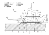
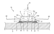
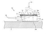
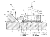
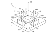
- FIG. 1 It is a main part plan view of the optical power supply converter which concerns on Example 1 of this invention. It is sectional drawing of the main part of the line II-II of FIG. It is a figure which shows the example of the optical power-feeding converter with a plurality of inclined end faces. It is a figure which shows the example of the optical power transfer converter which fixed the semiconductor light receiving element in the direction different from FIG. It is a figure which shows the optical power feed converter which provided the reflection part which concerns on Example 2.
- FIG. It is a figure which shows the optical power-feeding converter provided with the plurality of reflection parts which concerns on Example 2.
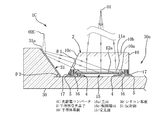
- FIG. It is a figure which shows the optical power feed converter which provided the reflection part which concerns on Example 3.
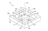
- FIG. It is a figure which shows the optical power-feeding converter provided with the plurality of reflection parts which concerns on Example 3.
- FIG. 1 It is a figure which shows the optical power-feeding converter provided with the plurality of reflection parts which concerns on Example 3.
- the optical power supply converter 1A has a semiconductor light receiving element 2 and a support substrate 3 that supports the semiconductor light receiving element 2.
- a pair of wirings 4 and 5 are formed on the support substrate 3.
- the semiconductor light receiving element 2 currents light (for example, infrared light in a wavelength region of 1 to 1.6 ⁇ m) emitted from emission points O1 and O2 corresponding to the positions of their emission ends via an optical fiber cable 6 or the like. Is converted to, and power is supplied to the outside via a pair of wires 4 and 5.
- the semiconductor light receiving element 2 is formed on the light absorption region 11a in the InGaAs layer 11 formed on the main surface 10a side and the InGaAs layer 11 with the (100) surface of the semiconductor substrate 10 which is an n-InP substrate as the main surface 10a.
- a light receiving unit 15 (photodiode) having a p-type diffusion region 12a in the formed n-InP layer 12 is provided.
- the n-InP layer 12 is covered with a dielectric film 13 (for example, a SiN film, a SiO2 film, etc.).
- the p-type diffusion region 12a is formed by doping a predetermined region of the n-InP layer 12 with Zn, for example, and the region of the InGaAs layer 11 in contact with the p-type diffusion region 12a corresponds to the light absorption region 11a.
- the p-type diffusion region 12a is formed, for example, in a regular octagon shape when viewed from the main surface 10a side, but may be formed in a polygonal shape including a rectangle or a circle.
- the semiconductor light receiving element 2 has an annular electrode 16 formed so as to border the p-type diffusion region 12a and connected to the p-type diffusion region 1a, and a substrate electrode 17 connected to the semiconductor substrate 10 outside the annular electrode 16.
- the annular electrode 16 is connected to the wiring 4, and the substrate electrode 17 is connected to the wiring 5. Then, a part of the light traveling in the semiconductor substrate 10 and incident on the light absorption region 11a of the light receiving portion 15 is converted into an electric current and supplied to the outside from the wirings 4 and 5 via the annular electrode 16 and the substrate electrode 17. Will be done.
- the semiconductor light receiving element 2 is fixed with the main surface 10a side facing the support substrate 2. Then, light is incident on the main surface 10a perpendicularly from the emission point O1 on the back surface 10b side of the semiconductor substrate 10 facing the main surface 10a, and reaches the light absorption region 11a.
- the semiconductor substrate 10 has an inclined end surface 10c formed so as to intersect the main surface 10a at an acute angle.
- the intersection angle ⁇ 1 with respect to the main surface 10a of the inclined end surface 10c can be set to an arbitrary acute angle, and here, for example, 62 °.
- the inclined end face 10c is formed by tilting the dicing blade in a posture usually perpendicular to the main surface 10a when dicing the semiconductor substrate 10 in the wafer state with the dicing blade.
- Light is incident on the inclined end surface 10c in parallel with the main surface 10a, and the light is refracted by the inclined end surface 10c to reach the light absorption region 11a.
- the inclined end face 10a is formed on a rough surface having fine irregularities having a height (depth) equal to or higher than the wavelength of the incident light by dicing, and the reflection of the incident light is reduced.
- the emission point O1 of the optical fiber cable that emits light perpendicularly incident on the main surface 10a is a semiconductor light receiving element 2 so that the entire light is incident on the light absorption region 11a in consideration of the emission angle of the emitted light.
- An appropriate separation distance is set from.
- the position of the emission point O2 of the optical fiber cable that emits the light incident on the inclined end surface 10c is such that the entire light is absorbed in the light absorption region 11a in consideration of the divergence angle of the emitted light and the refraction angle at the inclined end surface 10c. Is set appropriately to reach.
- the refraction angle on the optical axis is 8.4 °
- the position is 150 ⁇ m away from the semiconductor light receiving element 2 so as to be incident on the light absorption region 11a.
- the emission point O2 is set. In this way, the light incident on the inclined end surface 10c is made to reach the light absorption region 11a so as to overlap the light vertically incident on the main surface 10a, and the amount of light received by the light receiving unit 15 is increased, thereby increasing the optical power supply converter 1A. Increase the output current without increasing the output current.
- the semiconductor substrate 10 may include not only the inclined end surface 10c but also a plurality of inclined end surfaces such as an inclined end surface 10d for incident light from the emission point O3.
- the amount of light received by the light receiving unit 15 can be further increased to further increase the output current without increasing the optical power supply converter 1A.
- the rectangular semiconductor light receiving element 2 can have four inclined end faces corresponding to the four sides at the maximum, but it is made into a polygon shape such as a hexagon or an octagon and is inclined corresponding to each side of the polygon. It can also be configured so that light is incident on each end face.
- the semiconductor light receiving element 2 may be fixed to the support substrate 3 on the back surface 10b side with, for example, an epoxy-based adhesive 18.
- the light vertically incident on the main surface 10a from the emission point O1 is incident on the inside of the annular electrode 16 from the dielectric film 13 side and reaches the light absorption region 11a.
- the light incident parallel to the main surface 10a from the emission point O2 is refracted by the inclined end surface 10c and reaches the light absorption region 11a.
- the amount of light received by the light receiving unit 15 can be increased to increase the output current without increasing the optical power supply converter 1A. Further, as in FIG. 3, it is also possible to further increase the output current of the optical power supply converter 1A by injecting light from a plurality of inclined end faces 10c, 10d and the like. Although not shown, the annular electrode 16 and the substrate electrode 17 are connected to the wiring terminals corresponding to the wirings 4 and 5 by wire bonding.
- the optical power supply converter 1B obtained by modifying a part of the first embodiment will be described.
- the same reference numerals are given to the parts common to those in the first embodiment, and the description thereof will be omitted.
- a plurality of optical fiber cables are usually routed in a bundled state and connected to an optical power supply converter, but in the first embodiment, since the incident directions are different, the plurality of optical fiber cables are connected separately.
- optical fiber cables fixed to the emission points O1 and O2 are routed in a bundled state, one of them is fixed in a posture perpendicular to the main surface 10a at the emission point O1, and the other is fixed to the main surface 10a at the emission point O2. Fix in a posture parallel to.
- the optical fiber cable that incidents light perpendicularly to the main surface 10a from the emission point O1 and the other optical fiber cables in parallel without bending.
- the optical power supply converter 1B is provided with a reflecting portion 21 facing the inclined end surface 10c on the support substrate 3.
- the reflective portion 21 includes a reflective film 21b formed of a metal film containing, for example, Au, Al, etc. on the reflective surface of the base material 21a.
- the reflective surface of the base material 21a is tilted by 45 ° with respect to the support substrate 3 at a predetermined angle ⁇ 2.
- the position of the emission point O2B is set so that the incident region on the inclined end surface 10c is the same as in the case of FIG. Is arranged at the emission point O2B.
- the light incident on the inclined end surface 10c so as to overlap the light vertically incident on the main surface 10a reaches the light absorption region 11a, and the amount of light received by the light receiving unit 15 is increased, thereby increasing the optical power supply converter 1A. Increase the output current without doing. Since the light feeding converter 1B has parallel incident directions of light from a plurality of optical fiber cables, it is not necessary to bend the optical fiber cables and can be connected compactly.
- the light receiving amount of the light receiving unit 15 is increased and the optical power supply converter 1B is output without increasing.
- the current can be increased. Since the incident directions of light from the plurality of optical fiber cables are parallel, the plurality of optical fiber cables can be connected compactly without bending. Further, it is easy to arrange a plurality of reflecting portions so as to correspond to each side of the semiconductor light receiving element 2 having a polygonal shape other than the rectangle.
- the predetermined angle ⁇ 2 may be appropriately set according to the incident direction of the light.
- the optical power supply converter 1C obtained by modifying a part of the second embodiment will be described.
- the same reference numerals are given to the parts common to those of the second embodiment, and the description thereof will be omitted.
- the support substrate 3 of the second embodiment is, for example, a ceramic substrate, but the optical power supply converter 1C has a silicon (Si) substrate 30 instead of the support substrate 3.
- the surface of the silicon substrate 30 is the (100) plane, and as shown in FIG. 7, etching is performed from the surface by anisotropic etching using a known alkaline etching solution (KOH aqueous solution or the like) to (111).
- KOH aqueous solution or the like etching is performed from the surface by anisotropic etching using a known alkaline etching solution (KOH aqueous solution or the like) to (111).
- KOH aqueous solution or the like known alkaline etching solution
- the (111) surface of the silicon substrate 30 exposed by anisotropic etching is a smooth surface having an inclination of 54.7 ° with respect to the (100) surface as a predetermined angle ⁇ 3.
- a reflective portion 31 having a reflective film 31a formed on the (111) surface by a metal film containing, for example, Au, Al, or the like reflects the light emitted from the emission point O2C toward the inclined end surface 10c.
- the (111) surface inclined by 45 ° with respect to the surface is exposed by anisotropic etching on the silicon substrate 30 whose surface is angled from the (100) surface, and the same as in FIG. 4, although only one surface is used.
- the reflective portion 31 can also be formed.
- An appropriate position of the emission point O2C is set, and the optical fiber cable is arranged at the emission point O2C in parallel with the optical fiber cable that incidents light perpendicularly to the main surface 10a from the emission point O1.
- the light emitted from the emission point O2C is parallel to the light emitted from the emission point O1 and vertically incident on the main surface 10a, and the light reflected by the reflecting unit 31 is in a direction parallel to the main surface 10a. It tilts 19.4 ° and travels diagonally. Then, the light incident on the inclined end surface 10c is refracted by the inclined end surface 10c and reaches the light absorption region 11a.
- the light incident on the inclined end surface 10c so as to overlap the light vertically incident on the main surface 10a reaches the light absorption region 11a, and the amount of light received by the light receiving unit 15 is increased, thereby increasing the optical power supply converter 1C. Increase the output current without doing. Since the light feeding converter 1C has parallel incident directions of light from a plurality of optical fiber cables, it can be connected compactly without bending the optical fiber cables.
- the actions and effects of the optical power supply converters 1A to 1C will be described.
- the optical power transfer converters 1A to 1C superimpose the light incident on the main surface 10a and the light incident on the inclined end surface 10c and the like on the light receiving unit 15, convert the light into a current by the light receiving unit 15, and supply the light to the outside. Therefore, it is possible to receive and supply light emitted from a plurality of optical fiber cables without increasing the optical power supply converters 1A to 1C.
- the optical power supply converters 1B and 1C each include reflection portions 21, 31 and the like facing the inclined end face 10c and the like. Then, the light parallel to the light perpendicularly incident on the main surface 10a and incident on the reflecting portions 21, 31 and the like is reflected by the reflecting portions 21, 31 and the like toward the corresponding inclined end faces 10c and the like. Therefore, the emission points O1, O2B, O2C, etc. of the plurality of optical fiber cables can be arranged so as to emit in the direction perpendicular to the main surface 10a, and the optical fiber cables do not need to be bent. The optical fiber cable can be easily connected to 1C and can be connected compactly.
- the support substrate of the optical power supply converter 1C is a silicon substrate 30, and the reflecting portion 31 and the like are formed on the (111) surface of the silicon substrate 30. Since the reflecting portion 31 or the like can be formed flat at a constant inclination angle, it is possible to form the reflecting portion 31 or the like having high accuracy of the incident angle on the inclined end surface 10c or the like and having a high reflectance. Therefore, the light reflected by the reflecting unit 31 or the like having a high reflectance can be superimposed on the light perpendicularly incident on the main surface 10a and incident on the light receiving unit 15, so that the light feeding converter 1C does not need to be enlarged. It can receive light from multiple optical fiber cables and supply power.
- optical power supply converters 1A to 1C formed on the n-InP substrate as the semiconductor substrate 10 has been described, but the configuration of the present invention is not limited to this, and for example, light formed on a silicon substrate, a GaAs substrate, or the like. It can also be applied to a power supply converter.
- a person skilled in the art can carry out the embodiment in a form in which various modifications are added to the above embodiment without departing from the spirit of the present invention, and the present invention also includes such modified embodiments.
- Optical power supply converter 2 Semiconductor light receiving element 3: Supporting substrate 4, 5: Wiring 6: Optical fiber cable 10: Semiconductor substrate 10a: Main surface 10b: Back surface 10c to 10f: Inclined end surface 11: InGaAs layer 11a: Optical Absorption region 12: n-InP layer 12a: p-type diffusion region 13: Dielectric film 15: Light receiving part 16: Circular electrode 17: Substrate electrode 21 to 24: Reflection part 30: Silicon substrate 31 to 34: Reflection part O1 to O5 , O2B to O5B, O2C to O5C: Emission point
Landscapes
- Physics & Mathematics (AREA)
- Optics & Photonics (AREA)
- Engineering & Computer Science (AREA)
- General Physics & Mathematics (AREA)
- Computer Networks & Wireless Communication (AREA)
- Power Engineering (AREA)
- Optical Couplings Of Light Guides (AREA)
- Light Receiving Elements (AREA)
Priority Applications (3)
| Application Number | Priority Date | Filing Date | Title |
|---|---|---|---|
| US17/046,252 US11356054B2 (en) | 2020-07-06 | 2020-07-06 | Optical power supply converter |
| PCT/JP2020/026395 WO2022009265A1 (ja) | 2020-07-06 | 2020-07-06 | 光給電コンバータ |
| JP2020549716A JP6795870B1 (ja) | 2020-07-06 | 2020-07-06 | 光給電コンバータ |
Applications Claiming Priority (1)
| Application Number | Priority Date | Filing Date | Title |
|---|---|---|---|
| PCT/JP2020/026395 WO2022009265A1 (ja) | 2020-07-06 | 2020-07-06 | 光給電コンバータ |
Publications (1)
| Publication Number | Publication Date |
|---|---|
| WO2022009265A1 true WO2022009265A1 (ja) | 2022-01-13 |
Family
ID=73544751
Family Applications (1)
| Application Number | Title | Priority Date | Filing Date |
|---|---|---|---|
| PCT/JP2020/026395 Ceased WO2022009265A1 (ja) | 2020-07-06 | 2020-07-06 | 光給電コンバータ |
Country Status (3)
| Country | Link |
|---|---|
| US (1) | US11356054B2 (cg-RX-API-DMAC7.html) |
| JP (1) | JP6795870B1 (cg-RX-API-DMAC7.html) |
| WO (1) | WO2022009265A1 (cg-RX-API-DMAC7.html) |
Families Citing this family (6)
| Publication number | Priority date | Publication date | Assignee | Title |
|---|---|---|---|---|
| WO2022168201A1 (ja) | 2021-02-03 | 2022-08-11 | 株式会社京都セミコンダクター | 光給電コンバータ |
| JP7212983B1 (ja) * | 2022-03-04 | 2023-01-26 | 株式会社京都セミコンダクター | 半導体受光素子 |
| WO2024013781A1 (ja) * | 2022-07-11 | 2024-01-18 | 株式会社京都セミコンダクター | 光給電コンバータ |
| JP7201287B1 (ja) * | 2022-07-25 | 2023-01-10 | 株式会社京都セミコンダクター | 光給電コンバータ |
| WO2024095405A1 (ja) * | 2022-11-02 | 2024-05-10 | デクセリアルズ株式会社 | 光給電コンバータ |
| US20250231350A1 (en) * | 2024-01-12 | 2025-07-17 | Taiwan Semiconductor Manufacturing Company Limited | Fiber array unit including front side mirror and method of making the same |
Citations (10)
| Publication number | Priority date | Publication date | Assignee | Title |
|---|---|---|---|---|
| JPH1041536A (ja) * | 1996-07-19 | 1998-02-13 | Terumo Corp | 光電変換装置およびその製造方法 |
| JPH11163390A (ja) * | 1997-11-28 | 1999-06-18 | Fujitsu Ltd | 光モジュール |
| JP2002151668A (ja) * | 2000-11-10 | 2002-05-24 | Denso Corp | 光集積回路およびその製造方法 |
| JP2005294669A (ja) * | 2004-04-02 | 2005-10-20 | Nippon Telegr & Teleph Corp <Ntt> | 表面入射型受光素子 |
| JP2010114235A (ja) * | 2008-11-06 | 2010-05-20 | Nec Corp | 光電変換素子、光給電装置、及び光電変換素子の製造方法 |
| CN102201482A (zh) * | 2010-03-22 | 2011-09-28 | 无锡沃浦光电传感科技有限公司 | 量子阱红外探测器 |
| JP2013229513A (ja) * | 2012-04-26 | 2013-11-07 | Kyocera Corp | 太陽電池モジュールシステム |
| JP2018056382A (ja) * | 2016-09-29 | 2018-04-05 | 日産自動車株式会社 | 光給電システム |
| WO2019021362A1 (ja) * | 2017-07-25 | 2019-01-31 | 株式会社京都セミコンダクター | 端面入射型受光素子 |
| US20190348549A1 (en) * | 2017-02-21 | 2019-11-14 | Newport Corporation | High responsivity high bandwidth photodiode and method of manufacture |
Family Cites Families (3)
| Publication number | Priority date | Publication date | Assignee | Title |
|---|---|---|---|---|
| US4358676A (en) * | 1980-09-22 | 1982-11-09 | Optical Information Systems, Inc. | High speed edge illumination photodetector |
| JP2005150393A (ja) * | 2003-11-14 | 2005-06-09 | Sharp Corp | 受発光素子用サブマウント |
| US8742251B2 (en) | 2006-12-20 | 2014-06-03 | Jds Uniphase Corporation | Multi-segment photovoltaic power converter with a center portion |
-
2020
- 2020-07-06 US US17/046,252 patent/US11356054B2/en active Active
- 2020-07-06 JP JP2020549716A patent/JP6795870B1/ja active Active
- 2020-07-06 WO PCT/JP2020/026395 patent/WO2022009265A1/ja not_active Ceased
Patent Citations (10)
| Publication number | Priority date | Publication date | Assignee | Title |
|---|---|---|---|---|
| JPH1041536A (ja) * | 1996-07-19 | 1998-02-13 | Terumo Corp | 光電変換装置およびその製造方法 |
| JPH11163390A (ja) * | 1997-11-28 | 1999-06-18 | Fujitsu Ltd | 光モジュール |
| JP2002151668A (ja) * | 2000-11-10 | 2002-05-24 | Denso Corp | 光集積回路およびその製造方法 |
| JP2005294669A (ja) * | 2004-04-02 | 2005-10-20 | Nippon Telegr & Teleph Corp <Ntt> | 表面入射型受光素子 |
| JP2010114235A (ja) * | 2008-11-06 | 2010-05-20 | Nec Corp | 光電変換素子、光給電装置、及び光電変換素子の製造方法 |
| CN102201482A (zh) * | 2010-03-22 | 2011-09-28 | 无锡沃浦光电传感科技有限公司 | 量子阱红外探测器 |
| JP2013229513A (ja) * | 2012-04-26 | 2013-11-07 | Kyocera Corp | 太陽電池モジュールシステム |
| JP2018056382A (ja) * | 2016-09-29 | 2018-04-05 | 日産自動車株式会社 | 光給電システム |
| US20190348549A1 (en) * | 2017-02-21 | 2019-11-14 | Newport Corporation | High responsivity high bandwidth photodiode and method of manufacture |
| WO2019021362A1 (ja) * | 2017-07-25 | 2019-01-31 | 株式会社京都セミコンダクター | 端面入射型受光素子 |
Also Published As
| Publication number | Publication date |
|---|---|
| US20220006423A1 (en) | 2022-01-06 |
| JPWO2022009265A1 (cg-RX-API-DMAC7.html) | 2022-01-13 |
| US11356054B2 (en) | 2022-06-07 |
| JP6795870B1 (ja) | 2020-12-02 |
Similar Documents
| Publication | Publication Date | Title |
|---|---|---|
| JP6795870B1 (ja) | 光給電コンバータ | |
| US6924510B2 (en) | Silicon and silicon/germanium light-emitting device, methods and systems | |
| US5617439A (en) | Semiconductor laser device and semiconductor laser array device | |
| US12464854B2 (en) | Optical power supply converter | |
| US11843262B2 (en) | Optical power supply converter | |
| US11067761B2 (en) | Optical receptacle and optical module | |
| US20250237829A1 (en) | Optoelectronic component | |
| JP6205001B2 (ja) | 光電変換モジュール、及び、アクティブ光ケーブル | |
| JP6829923B1 (ja) | 受光素子ユニット | |
| JP7017829B1 (ja) | 光給電コンバータ | |
| JP7246808B1 (ja) | 光給電コンバータ | |
| JP7178153B1 (ja) | 光給電コンバータ | |
| JP7201287B1 (ja) | 光給電コンバータ | |
| CN118103996A (zh) | 光电器件 | |
| JP7178152B1 (ja) | 光給電コンバータ | |
| TWI858408B (zh) | 光電裝置 | |
| JP7178151B1 (ja) | 光給電コンバータ | |
| TWI667506B (zh) | 具有高輸出功率的光源裝置 | |
| JP4906545B2 (ja) | 発光装置および光伝送モジュール | |
| JP6652982B2 (ja) | 光モジュール | |
| CN117999658A (zh) | 光电装置 | |
| JP2019179171A (ja) | 光モジュール | |
| WO2024095405A1 (ja) | 光給電コンバータ | |
| JPS6032008A (ja) | 光ファイバ光電変換装置 |
Legal Events
| Date | Code | Title | Description |
|---|---|---|---|
| ENP | Entry into the national phase |
Ref document number: 2020549716 Country of ref document: JP Kind code of ref document: A |
|
| 121 | Ep: the epo has been informed by wipo that ep was designated in this application |
Ref document number: 20944041 Country of ref document: EP Kind code of ref document: A1 |
|
| NENP | Non-entry into the national phase |
Ref country code: DE |
|
| 122 | Ep: pct application non-entry in european phase |
Ref document number: 20944041 Country of ref document: EP Kind code of ref document: A1 |