WO2021256410A1 - 電子部品及び電子部品の製造方法 - Google Patents
電子部品及び電子部品の製造方法 Download PDFInfo
- Publication number
- WO2021256410A1 WO2021256410A1 PCT/JP2021/022437 JP2021022437W WO2021256410A1 WO 2021256410 A1 WO2021256410 A1 WO 2021256410A1 JP 2021022437 W JP2021022437 W JP 2021022437W WO 2021256410 A1 WO2021256410 A1 WO 2021256410A1
- Authority
- WO
- WIPO (PCT)
- Prior art keywords
- layer
- resin
- electrode layer
- external electrode
- end surface
- Prior art date
- Legal status (The legal status is an assumption and is not a legal conclusion. Google has not performed a legal analysis and makes no representation as to the accuracy of the status listed.)
- Ceased
Links
Images


Classifications
-
- H—ELECTRICITY
- H01—ELECTRIC ELEMENTS
- H01G—CAPACITORS; CAPACITORS, RECTIFIERS, DETECTORS, SWITCHING DEVICES, LIGHT-SENSITIVE OR TEMPERATURE-SENSITIVE DEVICES OF THE ELECTROLYTIC TYPE
- H01G9/00—Electrolytic capacitors, rectifiers, detectors, switching devices, light-sensitive or temperature-sensitive devices; Processes of their manufacture
- H01G9/004—Details
- H01G9/008—Terminals
- H01G9/012—Terminals specially adapted for solid capacitors
-
- H—ELECTRICITY
- H01—ELECTRIC ELEMENTS
- H01F—MAGNETS; INDUCTANCES; TRANSFORMERS; SELECTION OF MATERIALS FOR THEIR MAGNETIC PROPERTIES
- H01F27/00—Details of transformers or inductances, in general
- H01F27/28—Coils; Windings; Conductive connections
- H01F27/29—Terminals; Tapping arrangements for signal inductances
-
- H—ELECTRICITY
- H01—ELECTRIC ELEMENTS
- H01G—CAPACITORS; CAPACITORS, RECTIFIERS, DETECTORS, SWITCHING DEVICES, LIGHT-SENSITIVE OR TEMPERATURE-SENSITIVE DEVICES OF THE ELECTROLYTIC TYPE
- H01G4/00—Fixed capacitors; Processes of their manufacture
- H01G4/002—Details
- H01G4/228—Terminals
- H01G4/232—Terminals electrically connecting two or more layers of a stacked or rolled capacitor
-
- H—ELECTRICITY
- H01—ELECTRIC ELEMENTS
- H01G—CAPACITORS; CAPACITORS, RECTIFIERS, DETECTORS, SWITCHING DEVICES, LIGHT-SENSITIVE OR TEMPERATURE-SENSITIVE DEVICES OF THE ELECTROLYTIC TYPE
- H01G9/00—Electrolytic capacitors, rectifiers, detectors, switching devices, light-sensitive or temperature-sensitive devices; Processes of their manufacture
- H01G9/0029—Processes of manufacture
-
- H—ELECTRICITY
- H01—ELECTRIC ELEMENTS
- H01G—CAPACITORS; CAPACITORS, RECTIFIERS, DETECTORS, SWITCHING DEVICES, LIGHT-SENSITIVE OR TEMPERATURE-SENSITIVE DEVICES OF THE ELECTROLYTIC TYPE
- H01G4/00—Fixed capacitors; Processes of their manufacture
- H01G4/002—Details
- H01G4/018—Dielectrics
- H01G4/06—Solid dielectrics
- H01G4/08—Inorganic dielectrics
- H01G4/12—Ceramic dielectrics
-
- H—ELECTRICITY
- H01—ELECTRIC ELEMENTS
- H01G—CAPACITORS; CAPACITORS, RECTIFIERS, DETECTORS, SWITCHING DEVICES, LIGHT-SENSITIVE OR TEMPERATURE-SENSITIVE DEVICES OF THE ELECTROLYTIC TYPE
- H01G4/00—Fixed capacitors; Processes of their manufacture
- H01G4/002—Details
- H01G4/228—Terminals
- H01G4/232—Terminals electrically connecting two or more layers of a stacked or rolled capacitor
- H01G4/2325—Terminals electrically connecting two or more layers of a stacked or rolled capacitor characterised by the material of the terminals
-
- H—ELECTRICITY
- H01—ELECTRIC ELEMENTS
- H01G—CAPACITORS; CAPACITORS, RECTIFIERS, DETECTORS, SWITCHING DEVICES, LIGHT-SENSITIVE OR TEMPERATURE-SENSITIVE DEVICES OF THE ELECTROLYTIC TYPE
- H01G4/00—Fixed capacitors; Processes of their manufacture
- H01G4/30—Stacked capacitors
Definitions
- the present invention relates to an electronic component and a method for manufacturing the electronic component.
- a component having an external electrode provided on the surface of a body having an internal electrode is used.
- an external electrode of an electronic component for printing a conductive paste on a printed matter is formed via a metal mask composed of a hole portion and a mesh portion arranged so as to surround the outer periphery of the hole portion.
- a method for forming an external electrode of an electronic component wherein the outer periphery of the hole portion of the metal mask is inside the printed area of the printed matter and the outer periphery of the mesh portion is outside the printed area of the printed matter. Has been done.
- Patent Document 2 a pair of end faces facing each other, a pair of main surfaces extending so as to connect between the pair of end faces and facing each other, and a pair of main surfaces extending so as to connect the pair of main faces and facing each other.
- a method for manufacturing an electronic component including an element body having a pair of side surfaces and an external electrode formed on the end surface side of the element body, wherein the corner portion between the end surface and the main surface and the side surface is curved.
- It has a second paste layer forming step of forming a second paste layer by screen-printing a second conductive paste on one side or both sides of any one of the surfaces and a curved surface, and has a first paste layer.
- a method for manufacturing an electronic component in which a first paste layer or a second paste layer is formed so that the first paste layer and the second paste layer are joined on a curved surface in the forming step or the second paste layer forming step. Is disclosed.
- the first baking electrode and the second baking electrode formed by baking the first paste layer and the second paste layer are formed. Unevenness is generated on the surface of the electrode due to sintering of conductive metal particles.
- the first seizure electrode and the second It fills the minute irregularities of the baking electrode.
- the surface of the external electrode is smoothed in both the method for forming the external electrode of the electronic component described in Patent Document 1 and the method for manufacturing the electronic component described in Patent Document 2.
- the contact area between the external electrode and the conductive bonding material is unlikely to increase when the electronic component is mounted on the wiring board via the conductive bonding material such as solder. Therefore, there is a problem that the adhesion between the two is difficult to increase.
- the present invention has been made to solve the above problems, and when mounted on a wiring board via a conductive bonding material such as solder, the adhesion between the external electrode and the conductive bonding material is enhanced.
- the purpose is to provide electronic components.
- Another object of the present invention is to provide a method for manufacturing the above electronic components.
- the electronic component of the present invention includes a first end surface and a second end surface facing in the length direction, a first main surface and a second main surface facing in a thickness direction orthogonal to the length direction, and the length direction and the second main surface.
- a body having a first side surface and a second side surface facing each other in the width direction orthogonal to the thickness direction and having an internal electrode, and connected to the internal electrode exposed from the first end surface of the body.
- a second external electrode connected to the first external electrode provided on the first end surface and the internal electrode exposed from the second end surface of the element body, and provided on the second end surface.
- the first external electrode includes an external electrode, the first external electrode has a resin electrode layer containing a conductive component and a resin component, and the resin electrode layer of the first external electrode is the first end surface of the element body.
- a plurality of periodically arranged first portions having a first portion facing the entire surface and opposite to the first end surface of the element body in the first portion of the resin electrode layer of the first external electrode. It is characterized in that the convex portion of is provided.
- the method for manufacturing an electronic component of the present invention includes a first end surface and a second end surface facing in the length direction, a first main surface and a second main surface facing in the thickness direction orthogonal to the length direction, and the length.
- a second external electrode forming step of forming a second external electrode connected to the internal electrode exposed from the end face is provided, and in the first external electrode forming step, a conductive paste containing a conductive component and a resin component is provided. Is applied by a screen printing method to have a first portion facing the entire surface of the first end surface of the element body, and the side of the first part opposite to the first end surface of the element body. It is characterized in that a resin electrode layer is formed so that a plurality of convex portions are periodically arranged on the surface of the surface.
- an electronic component that enhances the adhesion between an external electrode and a conductive bonding material when it is mounted on a wiring board via a conductive bonding material such as solder. Further, according to the present invention, it is possible to provide a method for manufacturing the above electronic component.
- FIG. 3 is a schematic cross-sectional view showing a state in which the electrolytic capacitor shown in FIG. 2 is mounted on a wiring board via a conductive bonding material.
- FIG. 3 is a schematic cross-sectional view showing an enlarged region in the vicinity of the first external electrode in the electrolytic capacitor shown in FIG. 2.
- FIG. 3 is a schematic cross-sectional view showing an enlarged region in the vicinity of the second external electrode in the electrolytic capacitor shown in FIG. 2.
- the electronic component of the present invention and the method for manufacturing the electronic component of the present invention will be described.
- the present invention is not limited to the following configuration, and may be appropriately modified without departing from the gist of the present invention.
- a combination of a plurality of individual preferred configurations described below is also the present invention.
- the electronic component of the present invention has a first end surface and a second end surface facing in the length direction, a first main surface and a second main surface facing in a thickness direction orthogonal to the length direction, and the length direction and the second main surface.
- a body having a first side surface and a second side surface facing each other in the width direction orthogonal to the thickness direction and having an internal electrode, and connected to the internal electrode exposed from the first end surface of the body.
- a second external electrode connected to the first external electrode provided on the first end surface and the internal electrode exposed from the second end surface of the element body, and provided on the second end surface.
- the first external electrode includes an external electrode, the first external electrode has a resin electrode layer containing a conductive component and a resin component, and the resin electrode layer of the first external electrode is the first end surface of the element body.
- a plurality of periodically arranged first portions having a first portion facing the entire surface and opposite to the first end surface of the element body in the first portion of the resin electrode layer of the first external electrode. It is characterized in that the convex portion of is provided.
- the anode may be composed of a resin molded body having an electrolytic capacitor element and a sealing resin that seals the periphery of the electrolytic capacitor element
- the electrolytic capacitor element may be composed of a resin molded body.
- the internal electrode may include an anode, a dielectric layer provided on the surface of the anode, and a cathode facing the anode via the anode layer and having an electrolyte layer.
- the anode and the cathode may be used.
- Such electronic components correspond to electrolytic capacitors.
- an electrolytic capacitor will be described as an electronic component according to the first embodiment of the present invention.
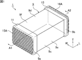
- FIG. 1 is a schematic perspective view showing an electronic component according to the first embodiment of the present invention.
- the electrolytic capacitor 1 has a resin molded body 9, a first external electrode 11, and a second external electrode 13.
- the length direction, the thickness direction, and the width direction are the directions defined by L, T, and W, respectively, as shown in FIG. 1 and the like.
- the length direction L, the thickness direction T, and the width direction W are orthogonal to each other.
- the resin molded body 9 corresponds to the element body in the electronic component of the present invention.
- the resin molded body 9 has a substantially rectangular parallelepiped shape, and has a width of a first end surface 9a and a second end surface 9b facing the length direction L, a first main surface 9c and a second main surface 9d facing the thickness direction T, and the like. It has a first side surface 9e and a second side surface 9f facing the direction W.
- the first end surface 9a and the second end surface 9b of the resin molded body 9 do not have to be exactly orthogonal to the length direction L. Further, the first main surface 9c and the second main surface 9d of the resin molded body 9 do not have to be exactly orthogonal to the thickness direction T. Further, the first side surface 9e and the second side surface 9f of the resin molded body 9 do not need to be exactly orthogonal to the width direction W.
- the first external electrode 11 is provided on the first end surface 9a of the resin molded body 9.
- the first external electrode 11 is one of each surface of the resin molded body 9 from the first end surface 9a to at least one surface of the first main surface 9c, the second main surface 9d, the first side surface 9e, and the second side surface 9f. It may extend over the department.
- the second external electrode 13 is provided on the second end surface 9b of the resin molded body 9.
- the second external electrode 13 is one of each of the first main surface 9c, the second main surface 9d, the first side surface 9e, and at least one surface of the second side surface 9f from the second end surface 9b of the resin molded body 9. It may extend over the department.
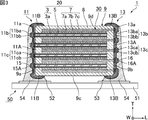
- FIG. 2 is a schematic cross-sectional view showing a portion corresponding to the line segments A1-A2 in FIG.
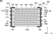
- the resin molded body 9 has a plurality of electrolytic capacitor elements 20 and a sealing resin 8 that seals the periphery of the plurality of electrolytic capacitor elements 20. More specifically, the resin molded body 9 has a laminated body 30 in which a plurality of electrolytic capacitor elements 20 are laminated in the thickness direction T, and a sealing resin 8 that seals the periphery of the laminated body 30. ing.
- the electrolytic capacitor elements 20 may be bonded to each other via, for example, a conductive adhesive called adhesive silver.
- the resin molded body 9 preferably has a plurality of electrolytic capacitor elements 20, but may have one electrolytic capacitor element 20.
- a support substrate such as a glass epoxy substrate may be provided on the bottom of the resin molded body 9.
- the bottom surface of the support substrate constitutes the first main surface 9c of the resin molded body 9.
- the electrolytic capacitor element 20 includes an anode 3, a dielectric layer 5, and a cathode 7.
- the anode 3 corresponds to the internal electrode in the electronic component of the present invention.
- the anode 3 has a valve acting metal substrate 3a at the center, and has a porous portion (not shown) on the surface.
- valve acting metal constituting the valve acting metal substrate 3a examples include simple metals such as aluminum, tantalum, niobium, titanium, zirconium, magnesium and silicon, or alloys containing at least one of these metals. Be done. Of these, aluminum or an aluminum alloy is preferable.
- the shape of the valve acting metal substrate 3a is preferably a flat plate shape, and more preferably a foil shape.
- the porous portion is preferably an etching layer in which the valve acting metal substrate 3a is etched with hydrochloric acid or the like.
- the thickness of the valve acting metal substrate 3a before the etching treatment is preferably 60 ⁇ m or more, and preferably 180 ⁇ m or less.
- the thickness of the core portion of the non-etched valve acting metal substrate 3a is preferably 10 ⁇ m or more, and preferably 70 ⁇ m or less.
- the thickness of the porous portion is designed according to the withstand voltage, capacitance, etc. required for the electrolytic capacitor 1, but in the cross section shown in FIG. 2, the porous portions provided on both sides of the valve acting metal substrate 3a.
- the total thickness of the portions is preferably 10 ⁇ m or more, and preferably 120 ⁇ m or less.
- the porous portion may be provided on one main surface of the valve acting metal substrate 3a.
- the anode 3 is exposed from the first end surface 9a of the resin molded body 9 and is connected to the first external electrode 11.
- the dielectric layer 5 is provided on the surface of the anode 3. More specifically, the dielectric layer 5 is provided on the surface of the porous portion.
- the dielectric layer 5 is preferably made of the oxide film of the valve acting metal described above.
- the valve acting metal substrate 3a is an aluminum foil
- the valve acting metal substrate 3a is anodized in an aqueous solution containing boric acid, phosphoric acid, adipic acid, or a sodium salt or ammonium salt thereof.
- an oxide film to be the dielectric layer 5 is formed. Since the dielectric layer 5 is formed along the surface of the porous portion, as a result, the dielectric layer 5 is provided with pores (recesses).
- the thickness of the dielectric layer 5 is designed according to the withstand voltage, capacitance, etc. required for the electrolytic capacitor 1, but is preferably 10 nm or more, and preferably 100 nm or less.
- the cathode 7 corresponds to an internal electrode in the electronic component of the present invention.
- the cathode 7 faces the anode 3 via the dielectric layer 5.
- the cathode 7 has an electrolyte layer. More specifically, the cathode 7 has a solid electrolyte layer 7a provided on the surface of the dielectric layer 5 as an electrolyte layer. Since the electrolytic capacitor 1 has the solid electrolyte layer 7a, it can be said that the electrolytic capacitor 1 is a solid electrolytic capacitor.
- the electrolytic capacitor 1 may be an electrolytic capacitor having an electrolytic solution instead of the solid electrolyte, or may be an electrolytic capacitor having both a solid electrolyte and an electrolytic solution.
- Examples of the constituent material of the solid electrolyte layer 7a include conductive polymers having pyrroles, thiophenes, anilines and the like as skeletons.
- Examples of the conductive polymer having a thiophene as a skeleton include poly (3,4-ethylenedioxythiophene) (PEDOT), and PEDOT: PSS complexed with polystyrene sulfonic acid (PSS) as a dopant. May be.
- the solid electrolyte layer 7a is a polymer film such as poly (3,4-ethylenedioxythiophene) on the surface of the dielectric layer 5 using, for example, a treatment liquid containing a monomer such as 3,4-ethylenedioxythiophene.
- a treatment liquid containing a monomer such as 3,4-ethylenedioxythiophene.
- the solid electrolyte layer 7a is formed by applying the above-mentioned treatment liquid or dispersion liquid to the surface of the dielectric layer 5 by a method such as a screen printing method, a sponge transfer method, an inkjet printing method, a dip coating method, a dispenser coating method, or a spray coating method. By working, it is formed in a predetermined area.
- a solid electrolyte layer for the inner layer that fills the pores (recesses) of the dielectric layer 5 is formed, and then a solid electrolyte layer for the outer layer that covers the entire dielectric layer 5 is formed. Is preferable.
- the thickness of the solid electrolyte layer 7a is preferably 2 ⁇ m or more, and preferably 20 ⁇ m or less.
- the cathode 7 further has a conductive layer 7b provided on the surface of the solid electrolyte layer 7a.
- the conductive layer 7b may be a conductive paste such as a carbon paste, a graphene paste, or a silver paste, which may be used in a screen printing method, a sponge transfer method, an inkjet printing method, a dip coating method, a dispenser coating method, a spray coating method, or the like. It is formed by coating the surface of the solid electrolyte layer 7a by the method.
- the conductive layer 7b is preferably a carbon layer, a graphene layer, or a silver layer formed by the above-mentioned method. Further, the conductive layer 7b may be a carbon layer or a composite layer in which a silver layer is provided on the graphene layer, or may be a carbon paste or a mixed layer in which graphene paste and silver paste are mixed.
- the thickness of the conductive layer 7b is preferably 2 ⁇ m or more, and preferably 20 ⁇ m or less.
- the cathode 7 may further have a cathode extraction layer 7c provided on the surface of the conductive layer 7b.
- the cathode extraction layer 7c is composed of, for example, a metal foil, a resin electrode layer, or the like.
- the metal foil is at least one metal selected from the group consisting of aluminum, copper, silver, and an alloy containing at least one of these metals as a main component. It is preferably composed of.
- the metal foil is made of the above-mentioned metal, the resistance of the metal foil is low, so that the ESR (equivalent series resistance) of the electrolytic capacitor 1 tends to be low.
- metal foil for example, a metal foil having a carbon coat, a titanium coat or the like applied to the surface by a film forming method such as sputtering or vapor deposition may be used. Of these, carbon-coated aluminum foil is preferably used.
- the thickness of the metal foil is preferably 20 ⁇ m or more, and preferably 50 ⁇ m or less, from the viewpoint of improving handleability in the manufacturing process, downsizing, and reducing ESR.
- the resin electrode layer may, for example, apply a conductive paste containing a conductive component and a resin component by a screen printing method, a sponge transfer method, an inkjet printing method, a dip coating method, or a dispenser. It is formed by coating the surface of the conductive layer 7b by a coating method, a spray coating method, or the like.
- the conductive paste used when forming the cathode extraction layer 7c preferably contains silver, copper, or nickel as the main component of the conductive component.
- the cathode drawer layer 7c When the cathode drawer layer 7c is formed by the printing method as described above, it can be made thinner than the metal foil.
- the thickness can be 20 ⁇ m or less.
- the cathode extraction layer 7c is preferably formed on the surface of the conductive layer 7b in a viscous state before the conductive layer 7b is dried.
- the cathode 7, here the cathode extraction layer 7c, is exposed from the second end surface 9b of the resin molded body 9 and is connected to the second external electrode 13.
- the conductive layer 7b may be exposed from the second end surface 9b of the resin molded body 9 and connected to the second external electrode 13.
- the sealing resin 8 contains at least a resin, and preferably contains a resin and a filler.
- epoxy resin epoxy resin, phenol resin, polyimide resin, silicone resin, polyamide resin, liquid crystal polymer and the like are preferably used.
- silica particles, alumina particles, metal particles and the like are preferably used.
- sealing resin 8 a material containing a solid epoxy resin, a phenol resin, and silica particles is preferably used.
- a resin mold such as a compression mold or a transfer mold is preferably used, and a compression mold is more preferably used.
- a molding method such as a dispensing method or a printing method is preferably used. Above all, it is preferable to seal the periphery of the laminated body 30 with the sealing resin 8 by the compression mold to obtain the resin molded body 9.
- the corners may be rounded.
- a method of rounding the corners of the resin molded body 9 for example, barrel polishing or the like is used.
- the first external electrode 11 is connected to the anode 3 exposed from the first end surface 9a of the resin molded body 9.
- the first external electrode 11 has a resin electrode layer 11a containing a conductive component and a resin component. Since the first external electrode 11 has the resin electrode layer 11a containing the resin component, in the region where the resin electrode layer 11a and the sealing resin 8 are in contact with each other, the adhesion between the two is improved, so that the reliability is improved. ..
- the resin electrode layer 11a has a first portion 11A facing the entire surface of the first end surface 9a of the resin molded body 9. That is, the first end surface 9a of the resin molded body 9 is not exposed from the first portion 11A of the resin electrode layer 11a.
- a plurality of periodically arranged convex portions 15 are provided on the surface of the first portion 11A of the resin electrode layer 11a on the side opposite to the first end surface 9a of the resin molded body 9.
- these convex portions are randomly arranged, whereas the plurality of convex portions 15 are periodic. Lined up in. Since the plurality of convex portions 15 are provided on the first portion 11A of the resin electrode layer 11a, the surface of the first external electrode 11 on the side opposite to the first end surface 9a of the resin molded body 9 becomes uneven.
- the resin electrode layer 11a is further formed from the first portion 11A on at least one surface of the first main surface 9c, the second main surface 9d, the first side surface 9e, and the second side surface 9f of the resin molded body 9. It may have a second portion 11B extending so as to face a part. More specifically, in the resin electrode layer 11a, the second portion 11B is the first main surface 9c, the second main surface 9d, the first side surface 9e, and the second side surface 9e of the resin molded body 9 from the first portion 11A. It may extend so as to face each part of all the surfaces of the side surface 9f, or the first main surface 9c, the second main surface 9d, the first side surface 9e, and the second side surface 9 of the resin molded body 9. It may extend so as to face a part of a part of the side surface 9f.
- the second portion 15 When the resin electrode layer 11a has the second portion 11B, when the plurality of convex portions 15 are provided on the surface of the second portion 11B of the resin electrode layer 11a opposite to the resin molded body 9, the second portion 15 is provided. 1
- the length of the external electrode 11 in the thickness direction T or the width direction W tends to be large. Therefore, when the electrolytic capacitor 1 is specified to have a predetermined size, the length of the resin molded body 9 in the thickness direction T or the width direction W tends to be small, and as a result, the thickness direction of the effective region of the electrolytic capacitor element 20. Since the length in T or the width direction W tends to be small, the capacitance tends to be small. From such a viewpoint, it is preferable that the surface of the second portion 11B of the resin electrode layer 11a opposite to the resin molded body 9 is not provided with the plurality of convex portions 15.
- the length of the portion of the resin molded body 9 facing the first main surface 9c in the length direction L and the length of the portion of the resin molded body 9 facing the second main surface 9d may be the same or different.
- the length in the length direction L of the portion facing the first side surface 9e of the resin molded body 9 and the length direction of the portion facing the second side surface 9f of the resin molded body 9 may be the same or different.
- the length of the portion of the resin molded body 9 facing the first main surface 9c and the second main surface 9d in the length direction L, and the first side surface 9e of the resin molded body 9 and The length of the portion facing the second side surface 9f in the length direction L may be the same or different.
- the conductive component of the resin electrode layer 11a preferably contains a simple substance of a metal such as silver, copper, nickel, or tin, or an alloy containing at least one of these metals as a main component.
- the resin component of the resin electrode layer 11a preferably contains an epoxy resin, a phenol resin, or the like as a main component.
- the resin electrode layer 11a preferably contains a conductive component of 80% by weight or more and 97% by weight or less, and a resin component of 3% by weight or more and 20% by weight or less. It is more preferable that the resin electrode layer 11a contains the conductive component in an amount of 85% by weight or more and 95% by weight or less, and the resin component in an amount of 5% by weight or more and 15% by weight or less. It is more preferable that the resin electrode layer 11a contains 90% by weight or more and 95% by weight or less of the conductive component and 5% by weight or more and 10% by weight or less of the resin component. It is particularly preferable that the resin electrode layer 11a contains a conductive component of 92% by weight or more and 95% by weight or less, and a resin component of 5% by weight or more and 8% by weight or less.
- the composition ratio of the conductive component and the resin component in the resin electrode layer is obtained as follows. First, in the cross section shown in FIG. 2, the resin electrode layer is observed by a scanning electron microscope / energy dispersive X-ray analysis (SEM / EDX), and a cross section image is acquired. Then, the area ratio of the conductive component and the resin component is calculated in the range of a square having a side of 100 ⁇ m in the cross-sectional image, for example. The area ratio of the conductive component and the resin component thus obtained is defined as the composition ratio of the conductive component and the resin component.
- SEM / EDX scanning electron microscope / energy dispersive X-ray analysis
- the resin electrode layer 11a is preferably formed by applying a conductive paste containing a conductive component and a resin component to a position facing the entire surface of the first end surface 9a of the resin molded body 9 by a screen printing method. Ru. At this time, so-called mesh marks due to the mesh shape of the screen printing plate are made to appear on the surface of the first portion 11A of the resin electrode layer 11a on the opposite side of the first end surface 9a of the resin molded body 9. As a result, a plurality of periodically arranged convex portions 15 can be formed on the surface of the first portion 11A of the resin electrode layer 11a on the side opposite to the first end surface 9a of the resin molded body 9.
- the resin electrode layer 11a may be formed by applying a conductive paste to a position facing the entire surface of the first end surface 9a of the resin molded body 9 by a sponge transfer method.
- the first external electrode 11 may further have an outer layer plating layer 11b provided along the surface of a plurality of convex portions 15 of the first portion 11A of the resin electrode layer 11a.
- each gap of the plurality of convex portions 15 is not completely filled with the outer layer plating layer 11b, and the surface of the outer layer plating layer 11b on the opposite side of the first end surface 9a of the resin molded body 9 is uneven.
- the surface of the first external electrode 11 on the side opposite to the first end surface 9a of the resin molded body 9 becomes uneven.
- a plurality of convex portions 15A exist in the uneven portion of the first external electrode 11, but the plurality of convex portions 15A have the plurality of convex portions 15 and the surfaces of the plurality of convex portions 15. It is composed of an outer layer plating layer 11b provided above. That is, the plurality of convex portions 15A are also periodically arranged in the same manner as the plurality of convex portions 15.
- the outer layer plating layer 11b may be provided on the surface of the second portion 11B of the resin electrode layer 11a.
- the outer layer plating layer 11b may have a single layer structure or a multi-layer structure.
- the outer layer plating layer 11b has a single layer structure, it is preferable that the outer layer plating layer 11b contains copper, nickel, or tin as a main component. As a result, the ESR of the electrolytic capacitor 1 tends to be low.
- the outer layer plating layer 11b may have a first outer layer plating layer 11ba and a second outer layer plating layer 11bb in this order from the resin electrode layer 11a side.
- the surfaces of the first outer layer plating layer 11ba and the second outer layer plating layer 11bb on the opposite side of the first end surface 9a of the resin molded body 9 become uneven.
- the first outer layer plating layer 11ba is preferably a nickel plating layer containing nickel as a main component.
- the nickel plating layer as the first outer layer plating layer 11ba is formed, for example, by performing electrolytic nickel plating on the resin electrode layer 11a.
- the second outer layer plating layer 11bb is preferably a tin plating layer containing tin as a main component.
- the tin-plated layer as the second outer layer plating layer 11bb is formed, for example, by immediately performing electrolytic tin plating so that the first outer layer plating layer 11ba does not come into contact with air after the formation of the first outer layer plating layer 11ba. ..
- the first external electrode 11 does not have to have the outer layer plating layer 11b.
- the first portion 11A of the resin electrode layer 11a is located on the surface of the first external electrode 11 opposite to the first end surface 9a of the resin molded body 9, and the plurality of convex portions 15A are the plurality of convex portions 15. Will consist of.
- the first external electrode 11 may further have an inner plating layer 11c provided between the anode 3 and the first portion 11A of the resin electrode layer 11a.
- the inner layer plating layer 11c is connected to the anode 3, and the first portion 11A of the resin electrode layer 11a is provided so as to cover the inner layer plating layer 11c.
- the anode 3 and the first portion 11A of the resin electrode layer 11a may be connected in a state where the inner layer plating layer 11c is not provided, but the contact resistance between the anode 3 and the first portion 11A of the resin electrode layer 11a.
- the value is high, the resistance between the anode 3 and the first portion 11A of the resin electrode layer 11a becomes low due to the provision of the inner layer plating layer 11c, so that the ESR of the electrolytic capacitor 1 tends to be low.
- the inner layer plating layer 11c may have a single layer structure or a multi-layer structure.
- the inner layer plating layer 11c has a single layer structure, it is preferable that the inner layer plating layer 11c contains copper, nickel, or silver as a main component. As a result, the ESR of the electrolytic capacitor 1 tends to be low.
- the inner layer plating layer 11c may have a first inner layer plating layer 11ca and a second inner layer plating layer 11cc in order from the anode 3 side.
- the first inner layer plating layer 11ca is preferably a nickel plating layer containing nickel as a main component.
- the nickel plating layer as the first inner layer plating layer 11ca is formed, for example, by subjecting the first end surface 9a of the resin molded body 9 to a zincate treatment and then performing a substitution plating treatment by electroless nickel plating.
- the zincate treatment is a treatment for removing oxides on the surface of a metal to be plated and forming a zinc film on the surface of the metal.
- the second inner layer plating layer 11cc is preferably a silver plating layer containing silver as a main component.
- the silver plating layer as the second inner layer plating layer 11cab is formed, for example, by immediately performing electrolytic silver plating so that the first inner layer plating layer 11ca does not come into contact with air after the formation of the first inner layer plating layer 11ca. ..
- the first external electrode 11 does not have to have the inner plating layer 11c.
- the first portion 11A of the resin electrode layer 11a is connected to the anode 3.
- the second external electrode 13 is connected to the cathode 7 exposed from the second end surface 9b of the resin molded body 9, here, the cathode extraction layer 7c.
- the second external electrode 13 preferably has a resin electrode layer 13a containing a conductive component and a resin component. Since the second external electrode 13 has the resin electrode layer 13a containing the resin component, in the region where the resin electrode layer 13a and the sealing resin 8 are in contact with each other, the adhesion between the two is improved, so that the reliability is improved. ..
- the resin electrode layer 13a preferably has a first portion 13A facing the entire surface of the second end surface 9b of the resin molded body 9. In this case, the second end surface 9b of the resin molded body 9 is not exposed from the first portion 13A of the resin electrode layer 13a.
- a plurality of periodically arranged convex portions 16 are provided on the surface of the first portion 13A of the resin electrode layer 13a on the side opposite to the second end surface 9b of the resin molded body 9. Since the plurality of convex portions 16 are provided on the first portion 13A of the resin electrode layer 13a, the surface of the second external electrode 13 on the side opposite to the second end surface 9b of the resin molded body 9 becomes uneven.
- the resin electrode layer 13a is further formed from the first portion 13A on at least one surface of the first main surface 9c, the second main surface 9d, the first side surface 9e, and the second side surface 9f of the resin molded body 9. It may have a second portion 13B extending so as to face a part. More specifically, in the resin electrode layer 13a, the second portion 13B is the first main surface 9c, the second main surface 9d, the first side surface 9e, and the second side surface 9e of the resin molded body 9 from the first portion 13A. It may extend so as to face each part of all the surfaces of the side surface 9f, or the first main surface 9c, the second main surface 9d, the first side surface 9e, and the second side surface 9 of the resin molded body 9. It may extend so as to face a part of a part of the side surface 9f.
- the second portion 16 When the resin electrode layer 13a has the second portion 13B, when the plurality of convex portions 16 are provided on the surface of the second portion 13B of the resin electrode layer 13a opposite to the resin molded body 9, the second portion 16 is provided. 2
- the length of the external electrode 13 in the thickness direction T or the width direction W tends to be large. Therefore, when the electrolytic capacitor 1 is specified to have a predetermined size, the length of the resin molded body 9 in the thickness direction T or the width direction W tends to be small, and as a result, the thickness direction of the effective region of the electrolytic capacitor element 20. Since the length in T or the width direction W tends to be small, the capacitance tends to be small. From such a viewpoint, it is preferable that the surface of the second portion 13B of the resin electrode layer 13a on the opposite side of the resin molded body 9 is not provided with the plurality of convex portions 16.
- the length of the portion of the resin molded body 9 facing the first main surface 9c in the length direction L and the length of the portion of the resin molded body 9 facing the second main surface 9d may be the same or different.
- the length in L may be the same or different.
- the length of the portion of the resin molded body 9 facing the first main surface 9c and the second main surface 9d in the length direction L, and the first side surface 9e of the resin molded body 9 and The length of the portion facing the second side surface 9f in the length direction L may be the same or different.
- the conductive component of the resin electrode layer 13a preferably contains a simple substance of a metal such as silver, copper, nickel, or tin, or an alloy containing at least one of these metals as a main component.
- the resin component of the resin electrode layer 13a preferably contains an epoxy resin, a phenol resin, or the like as a main component.
- the resin electrode layer 13a preferably contains a conductive component of 80% by weight or more and 97% by weight or less, and a resin component of 3% by weight or more and 20% by weight or less. It is more preferable that the resin electrode layer 13a contains the conductive component in an amount of 85% by weight or more and 95% by weight or less, and the resin component in an amount of 5% by weight or more and 15% by weight or less. It is more preferable that the resin electrode layer 13a contains 90% by weight or more and 95% by weight or less of the conductive component and 5% by weight or more and 10% by weight or less of the resin component. It is particularly preferable that the resin electrode layer 13a contains a conductive component of 92% by weight or more and 95% by weight or less, and a resin component of 5% by weight or more and 8% by weight or less.
- the resin electrode layer 13a is preferably formed by applying a conductive paste containing a conductive component and a resin component to a position facing the entire surface of the second end surface 9b of the resin molded body 9 by a screen printing method. Ru.
- the mesh marks at the time of screen printing are made to appear on the surface of the first portion 13A of the resin electrode layer 13a on the opposite side of the second end surface 9b of the resin molded body 9.
- a plurality of periodically arranged convex portions 16 can be formed on the surface of the first portion 13A of the resin electrode layer 13a on the side opposite to the second end surface 9b of the resin molded body 9.
- the resin electrode layer 13a may be formed by applying a conductive paste to a position facing the entire surface of the second end surface 9b of the resin molded body 9 by a sponge transfer method.
- the second external electrode 13 may further have an outer layer plating layer 13b provided along the surface of a plurality of convex portions 16 of the first portion 13A of the resin electrode layer 13a.
- each gap of the plurality of convex portions 16 is not completely filled with the outer layer plating layer 13b, and the surface of the outer layer plating layer 13b on the opposite side of the second end surface 9b of the resin molded body 9 is uneven.
- the surface of the second external electrode 13 on the side opposite to the second end surface 9b of the resin molded body 9 becomes uneven.
- a plurality of convex portions 16A exist in the uneven portion of the second external electrode 13, but the plurality of convex portions 16A have the plurality of convex portions 16 and the surfaces of the plurality of convex portions 16. It is composed of an outer layer plating layer 13b provided above. That is, the plurality of convex portions 16A are also periodically arranged in the same manner as the plurality of convex portions 16.
- the outer layer plating layer 13b may be provided on the surface of the second portion 13B of the resin electrode layer 13a.
- the outer layer plating layer 13b may have a single layer structure or a multi-layer structure.
- the outer layer plating layer 13b has a single layer structure, it is preferable that the outer layer plating layer 13b contains copper, nickel, or tin as a main component. As a result, the ESR of the electrolytic capacitor 1 tends to be low.
- the outer layer plating layer 13b may have a first outer layer plating layer 13ba and a second outer layer plating layer 13bb in this order from the resin electrode layer 13a side.
- the surfaces of the first outer layer plating layer 13ba and the second outer layer plating layer 13bb on the opposite side of the second end surface 9b of the resin molded body 9 become uneven.
- the first outer layer plating layer 13ba is preferably a nickel plating layer containing nickel as a main component.
- the nickel plating layer as the first outer layer plating layer 13ba is formed, for example, by performing electrolytic nickel plating on the resin electrode layer 13a.
- the second outer layer plating layer 13bb is preferably a tin plating layer containing tin as a main component.
- the tin-plated layer as the second outer layer plating layer 13bb is formed, for example, by immediately performing electrolytic tin plating so that the first outer layer plating layer 13ba does not come into contact with air after the formation of the first outer layer plating layer 13ba. ..
- the second external electrode 13 does not have to have the outer layer plating layer 13b.
- the first portion 13A of the resin electrode layer 13a is located on the surface of the second external electrode 13 opposite to the second end surface 9b of the resin molded body 9, and the plurality of convex portions 16A are the plurality of convex portions 16. Will consist of.
- the second external electrode 13 may further have an inner plating layer 13c provided between the cathode 7 and the first portion 13A of the resin electrode layer 13a.
- the inner layer plating layer 13c is connected to the cathode 7, and the first portion 13A of the resin electrode layer 13a is provided so as to cover the inner layer plating layer 13c.
- the cathode 7 and the first portion 13A of the resin electrode layer 13a may be connected in a state where the inner layer plating layer 13c is not provided, but the contact resistance between the cathode 7 and the first portion 13A of the resin electrode layer 13a.
- the value is high, the resistance between the cathode 7 and the first portion 13A of the resin electrode layer 13a becomes low due to the provision of the inner layer plating layer 13c, so that the ESR of the electrolytic capacitor 1 tends to be low.
- the inner layer plating layer 13c may have a single layer structure or a multi-layer structure.
- the inner layer plating layer 13c has a single layer structure, it is preferable that the inner layer plating layer 13c contains copper, nickel, or silver as a main component. As a result, the ESR of the electrolytic capacitor 1 tends to be low.
- the inner layer plating layer 13c may have a first inner layer plating layer 13ca and a second inner layer plating layer 13cc in order from the cathode 7 side.
- the first inner layer plating layer 13ca is preferably a nickel plating layer containing nickel as a main component.
- the nickel plating layer as the first inner layer plating layer 13ca is formed on the second end surface 9b of the resin molded body 9 in the same manner as the nickel plating layer as the first inner layer plating layer 11ca, but is zincated. It is not necessary to perform the processing. However, when the cathode 7, here the cathode extraction layer 7c, contains aluminum as a main component, it is preferable to perform a zincate treatment.
- the second inner layer plating layer 13cc is preferably a silver plating layer containing silver as a main component.
- the silver plating layer as the second inner layer plating layer 13cab is formed, for example, by immediately performing electrolytic silver plating so that the first inner layer plating layer 13ca does not come into contact with air after the formation of the first inner layer plating layer 13ca. ..
- the second external electrode 13 does not have to have the inner plating layer 13c.
- the first portion 13A of the resin electrode layer 13a is connected to the cathode 7.
- FIG. 3 is a schematic cross-sectional view showing a state in which the electrolytic capacitor shown in FIG. 2 is mounted on a wiring board via a conductive bonding material.
- the electrolytic capacitor 1 is mounted on the wiring board 50 via a conductive bonding material 54 such as solder.
- the wiring board 50 includes a printed circuit board 51, a land electrode 52 provided on the surface of the printed circuit board 51, and a land electrode 53 provided on the surface of the printed circuit board 51 at a position different from the land electrode 52. is doing.
- the first external electrode 11 and the land electrode 52 are electrically connected via the conductive bonding material 54
- the second external electrode is electrically connected.
- the electrode 13 and the land electrode 53 are electrically connected via the conductive bonding material 54.
- a plurality of convex portions 15 are provided on the surface of the first portion 11A of the resin electrode layer 11a of the first external electrode 11 on the side opposite to the first end surface 9a of the resin molded body 9. 1
- the surface of the external electrode 11, here, the outer layer plating layer 11b, on the side opposite to the first end surface 9a of the resin molded body 9, is uneven. Therefore, when the electrolytic capacitor 1 is mounted on the wiring board 50 via the conductive bonding material 54, the contact area between the first external electrode 11 and the conductive bonding material 54 becomes large, and the anchor effect is exhibited. Therefore, the adhesion between the first external electrode 11 and the conductive bonding material 54 is enhanced. Further, when measuring the electrical characteristics of the electrolytic capacitor 1, the measuring probe can be brought into contact with the plurality of convex portions 15A existing in the uneven portion of the first external electrode 11, so that the measurement is stabilized.
- a plurality of convex portions 16 are provided on the surface of the first portion 13A of the resin electrode layer 13a of the second external electrode 13 on the side opposite to the second end surface 9b of the resin molded body 9. 2
- the surface of the external electrode 13, here, the outer layer plating layer 13b, on the side opposite to the second end surface 9b of the resin molded body 9, is uneven. Therefore, when the electrolytic capacitor 1 is mounted on the wiring board 50 via the conductive bonding material 54, the contact area between the second external electrode 13 and the conductive bonding material 54 becomes large, and the anchor effect is exhibited. Therefore, the adhesion between the second external electrode 13 and the conductive bonding material 54 is enhanced. Further, when measuring the electrical characteristics of the electrolytic capacitor 1, the measuring probe can be brought into contact with the plurality of convex portions 16A existing in the uneven portion of the second external electrode 13, so that the measurement is stabilized.
- the form of the first external electrode 11, particularly the form of the resin electrode layer 11a will be described.
- the plurality of convex portions 15 are preferably arranged periodically in at least one direction and intersect with each other. It is more preferable that they are arranged periodically in a plurality of directions.
- the plurality of convex portions 15 are periodically arranged in a plurality of intersecting directions, for example, an embodiment in which the plurality of convex portions 15 are arranged in a matrix can be mentioned.
- the plurality of convex portions 15 may be arranged in a matrix along the thickness direction T and the width direction W.
- the plurality of convex portions 15A are preferably arranged periodically in at least one direction, and a plurality of intersecting portions thereof are preferable. It is more preferable that they are arranged periodically in the direction of.
- the plurality of convex portions 15A are periodically arranged in a plurality of intersecting directions, for example, an embodiment in which the plurality of convex portions 15A are arranged in a matrix can be mentioned. In this case, the plurality of convex portions 15A may be arranged in a matrix along the thickness direction T and the width direction W.
- the plurality of convex portions 15 are provided in a region of 80 area% or more of the surface of the first portion 11A of the resin electrode layer 11a opposite to the first end surface 9a of the resin molded body 9. Further, it is more preferable that the plurality of convex portions 15 are provided on the entire surface of the first portion 11A of the resin electrode layer 11a on the side opposite to the first end surface 9a of the resin molded body 9.
- the plurality of convex portions 15A are provided in a region of 80 area% or more of the surface of the first external electrode 11 opposite to the first end surface 9a of the resin molded body 9. Further, it is more preferable that the plurality of convex portions 15A are provided on the entire surface of the first external electrode 11 on the side opposite to the first end surface 9a of the resin molded body 9.
- the cross-sectional shape of the plurality of convex portions 15 may be a polygonal shape or a circular shape.
- the cross-sectional shape of the plurality of convex portions 15A may be a polygonal shape or a circular shape.
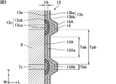
- FIG. 4 is a schematic cross-sectional view showing an enlarged region in the vicinity of the first external electrode in the electrolytic capacitor shown in FIG.
- the cross-sectional shapes of the plurality of convex portions 15 are from the first end surface 9a side to the opposite side to the first end surface 9a of the resin molded body 9. It is preferable to have a so-called tapered shape in which the length in the thickness direction T becomes smaller toward the surface.
- the ridgeline of the plurality of convex portions 15 may be a curved line or a straight line.
- the cross-sectional shapes of the plurality of convex portions 15 are from the first end surface 9a side to the opposite side to the first end surface 9a of the resin molded body 9. It may have a shape in which the length in the thickness direction T is constant toward.
- the cross-sectional shapes of the plurality of convex portions 15A are different from the first end surface 9a side of the resin molded body 9 to the first end surface 9a. It is preferable to have a tapered shape in which the length in the thickness direction T decreases toward the opposite side.
- the ridgeline of the plurality of convex portions 15A may be a curved line or a straight line.
- the cross-sectional shapes of the plurality of convex portions 15A are from the first end surface 9a side to the opposite side to the first end surface 9a of the resin molded body 9. It may have a shape in which the length in the thickness direction T is constant toward.
- the surface of the first portion 11A of the resin electrode layer 11a has an arithmetic average roughness Ra defined by JIS B 0601: 2013. It is preferably 20 ⁇ m or more and 100 ⁇ m or less.
- Ra arithmetic average roughness defined by JIS B 0601: 2013. It is preferably 20 ⁇ m or more and 100 ⁇ m or less.
- the lengths of the plurality of convex portions 15 in the length direction L become relatively large. Therefore, when the electrolytic capacitor 1 is mounted on the wiring board 50 via the conductive bonding material 54, the contact area between the first external electrode 11 and the conductive bonding material 54 becomes sufficiently large, and the anchor effect is sufficient. Therefore, the adhesion between the first external electrode 11 and the conductive bonding material 54 is sufficiently enhanced. Further, when the outer layer plating layer 11b is formed, it becomes easy to form along the surface of the plurality of convex portions 15.
- the surface of the first portion 11A of the resin electrode layer 11a has a bottom surface 11Aa located between each of the plurality of convex portions 15. , It is preferable that the top surface 11Ab of the plurality of convex portions 15 is present.
- the contact area between the first external electrode 11 and the conductive bonding material 54 becomes sufficiently large, and the anchor effect is obtained. Since it is sufficiently exhibited, the adhesion between the first external electrode 11 and the conductive bonding material 54 is sufficiently enhanced.
- the bottom surface 11Aa is a surface located between each of the plurality of convex portions 15 when the cross section shown in FIG. 4 is viewed, and the length of each surface is long. It includes a point located most on the first end surface 9a side of the resin molded body 9 in the vertical direction L, and indicates a range in which the arithmetic average roughness Ra defined by JIS B 0601: 2013 is 5 ⁇ m or less.
- the top surface 11Ab is the most resin molded body 9 in the length direction L in each of the plurality of convex portions 15 when the cross section shown in FIG. 4 is viewed. It includes a point located on the opposite side of the first end surface 9a, and refers to a range in which the arithmetic mean roughness Ra defined by JIS B 0601: 2013 is 5 ⁇ m or less.
- the length Taa of the bottom surface 11Aa in the thickness direction T is preferably 50 ⁇ m or more and 200 ⁇ m or less.
- the distance between the plurality of convex portions 15 in the thickness direction T becomes relatively large. Therefore, when the electrolytic capacitor 1 is mounted on the wiring board 50 via the conductive bonding material 54, the conductive bonding material 54 is provided between each of the plurality of convex portions 15A existing in the uneven portion of the first external electrode 11. Is easy to get in. Further, when the outer layer plating layer 11b is formed, it becomes easy to form along the surface of the plurality of convex portions 15.
- the length Taa of the bottom surface 11Aa in the thickness direction T is for the bottom surface 11Aa at 20 of the bottom surfaces 11Aa when there are 20 or more locations, and for all the bottom surfaces 11Aa when the bottom surface 11Aa is not present at 20 or more locations. , Is determined by the average value of the lengths of the bottom surface 11Aa in the thickness direction T.
- the shortest distance Tpa in the thickness direction T between the top surfaces 11Abs of two adjacent convex portions 15 among the plurality of convex portions 15 is preferably 50 ⁇ m or more and 100 ⁇ m or less.
- the distance between the plurality of convex portions 15 in the thickness direction T becomes relatively large. Therefore, when the electrolytic capacitor 1 is mounted on the wiring board 50 via the conductive bonding material 54, the conductive bonding material 54 is provided between each of the plurality of convex portions 15A existing in the uneven portion of the first external electrode 11. Is easy to get in. Further, when the outer layer plating layer 11b is formed, it becomes easy to form along the surface of the plurality of convex portions 15.
- the shortest distance Tpa in the thickness direction T between the apex surfaces 11Ab is such that when there are 20 or more regions between the apex surfaces 11Ab, there are no more than 20 regions between the apex surfaces 11Ab with respect to 20 or more regions. In the case, it is determined by the average value of the shortest distances in the thickness direction T between the top surfaces 11Ab for all regions.
- the shortest distance Tpa in the thickness direction T between the top surfaces 11Ab is larger than the length Taa in the thickness direction T of the bottom surface 11Aa.
- the conductive bonding material is provided between each of the plurality of convex portions 15A existing in the uneven portion of the first external electrode 11. 54 is easy to enter. Further, when the outer layer plating layer 11b is formed, it becomes easy to form along the surface of the plurality of convex portions 15.
- the shortest distance Tpa in the thickness direction T between the top surfaces 11Ab may be the same as the length Taa in the thickness direction T of the bottom surface 11Aa, or may be smaller than the length Taa in the thickness direction T of the bottom surface 11Aa.
- the length Tba of the top surface 11Ab in the thickness direction T is preferably 10 ⁇ m or more and 100 ⁇ m or less.
- the contact area between the first external electrode 11 and the conductive bonding material 54 becomes sufficiently large, and the anchor effect is obtained. Since it is sufficiently exhibited, the adhesion between the first external electrode 11 and the conductive bonding material 54 is sufficiently enhanced. Further, when the outer layer plating layer 11b is formed, it becomes easy to form along the surface of the plurality of convex portions 15.
- the length Tba of the apex surface 11Ab in the thickness direction T is such that when the apex surface 11Ab is present at 20 or more locations, the apex surface 11Ab is 20 or more, and when the apex surface 11Ab is not present at 20 or more locations, all the apexes are apex. It is determined by the average value of the lengths of the top surface 11Ab in the thickness direction T with respect to the surface 11Ab.
- the length Taa of the bottom surface 11Aa in the thickness direction T is larger than the length Tba of the top surface 11Ab in the thickness direction T.
- the conductive bonding material is provided between each of the plurality of convex portions 15A existing in the uneven portion of the first external electrode 11. 54 is easy to enter. Further, when the outer layer plating layer 11b is formed, it becomes easy to form along the surface of the plurality of convex portions 15.
- the length Taa of the bottom surface 11Aa in the thickness direction T may be the same as the length Tba of the top surface 11Ab in the thickness direction T, or may be smaller than the length Tba of the top surface 11Ab in the thickness direction T.
- the shortest distance La in the length direction L between the bottom surface 11Aa and the first end surface 9a is preferably 10 ⁇ m or more and 50 ⁇ m or less.
- each of the plurality of convex portions 15 is provided at a position facing the anode 3 in the length direction L, but may not be provided at a position facing the anode 3 in the length direction L. ..
- each of the plurality of convex portions 15 may be provided at a position facing the region between the anodes 3 in the length direction L.
- each of the plurality of convex portions 15 is provided at a position facing the inner layer plating layer 11c in the length direction L, but is provided at a position facing the inner layer plating layer 11c in the length direction L. It does not have to be.
- each of the plurality of convex portions 15 may be provided at a position facing the region between the inner layer plating layers 11c and the length direction L.
- the cross-sectional shapes of the plurality of convex portions 15 are directed from the first end surface 9a side of the resin molded body 9 to the opposite side to the first end surface 9a. It is preferable that the shape is tapered so that the length in the width direction W is small.
- the ridgeline of the plurality of convex portions 15 may be a curved line or a straight line.
- the cross-sectional shape of the plurality of convex portions 15 is the width direction W from the first end surface 9a side of the resin molded body 9 toward the side opposite to the first end surface 9a. It may have a shape in which the length is constant.
- the cross-sectional shapes of the plurality of convex portions 15A are from the first end surface 9a side of the resin molded body 9 toward the opposite side to the first end surface 9a. It is preferable to have a tapered shape in which the length in the width direction W becomes small.
- the ridgeline of the plurality of convex portions 15A may be a curved line or a straight line.
- the cross-sectional shape of the plurality of convex portions 15A is the width direction W from the first end surface 9a side of the resin molded body 9 toward the side opposite to the first end surface 9a. It may have a shape in which the length is constant.
- the surface of the first portion 11A of the resin electrode layer 11a When looking at the cross section along the length direction L and the width direction W, the surface of the first portion 11A of the resin electrode layer 11a has an arithmetic average roughness Ra defined by JIS B 0601: 2013 of 20 ⁇ m or more and 100 ⁇ m or less. It is preferable to have.
- the arithmetic average roughness Ra of the surface of the first portion 11A of the resin electrode layer 11a is seen when the cross section along the length direction L and the thickness direction T is seen, and when the cross section along the length direction L and the width direction W is seen. It may be the same or different from time to time.
- the length of the bottom surface in the width direction W is preferably 50 ⁇ m or more and 200 ⁇ m or less.
- the length of the bottom surface in the width direction W may be the same as or different from the length Taa of the bottom surface 11Aa in the thickness direction T.
- the shortest distance in the width direction W between the top surfaces of two adjacent convex portions 15 among the plurality of convex portions 15 is preferably 50 ⁇ m or more and 100 ⁇ m or less.
- the shortest distance between the top surfaces in the width direction W is larger than the length in the width direction W of the bottom surface.
- the shortest distance between the top surfaces in the width direction W may be the same as the length in the width direction W of the bottom surface, or may be smaller than the length in the width direction W of the bottom surface.
- the shortest distance in the width direction W between the top surfaces may be the same as or different from the shortest distance Tpa in the thickness direction T between the top surfaces 11Ab.
- the length of the top surface in the width direction W is preferably 10 ⁇ m or more and 100 ⁇ m or less.
- the length of the top surface in the width direction W may be the same as or different from the length Tba of the top surface 11Ab in the thickness direction T.
- the length of the bottom surface in the width direction W is larger than the length of the top surface in the width direction W.
- the length of the bottom surface in the width direction W may be the same as the length of the top surface in the width direction W, or may be smaller than the length of the top surface in the width direction W.
- the cross section along the length direction L and the thickness direction T, the cross section along the length direction L and the width direction W, and the cross section along the thickness direction T and the width direction W are scanning electron microscopes. Observed by (SEM). Then, various parameters of the resin electrode layer 11a such as the arithmetic mean roughness Ra of the surface of the first portion 11A of the resin electrode layer 11a as described above are measured from the cross-sectional image taken by the scanning electron microscope.
- the plurality of convex portions 16 are preferably arranged periodically in at least one direction and intersect with each other. It is more preferable that they are arranged periodically in a plurality of directions.
- the plurality of convex portions 16 are periodically arranged in a plurality of intersecting directions, for example, an embodiment in which the plurality of convex portions 16 are arranged in a matrix can be mentioned. In this case, the plurality of convex portions 16 may be arranged in a matrix along the thickness direction T and the width direction W.
- the plurality of convex portions 16A are preferably arranged periodically in at least one direction, and a plurality of intersecting portions thereof are preferable. It is more preferable that they are arranged periodically in the direction of.
- the plurality of convex portions 16A are periodically arranged in a plurality of intersecting directions, for example, an embodiment in which the plurality of convex portions 16A are arranged in a matrix can be mentioned. In this case, the plurality of convex portions 16A may be arranged in a matrix along the thickness direction T and the width direction W.
- the plurality of convex portions 16 are provided in a region of 80 area% or more of the surface of the first portion 13A of the resin electrode layer 13a opposite to the second end surface 9b of the resin molded body 9. Further, it is more preferable that the plurality of convex portions 16 are provided on the entire surface of the first portion 13A of the resin electrode layer 13a on the side opposite to the second end surface 9b of the resin molded body 9.
- the plurality of convex portions 16A are provided in a region of 80 area% or more of the surface of the second external electrode 13 opposite to the second end surface 9b of the resin molded body 9. Further, it is more preferable that the plurality of convex portions 16A are provided on the entire surface of the second external electrode 13 on the side opposite to the second end surface 9b of the resin molded body 9.
- the cross-sectional shape of the plurality of convex portions 16 may be a polygonal shape or a circular shape.
- the cross-sectional shape of the plurality of convex portions 16A may be a polygonal shape or a circular shape.
- FIG. 5 is a schematic cross-sectional view showing an enlarged region in the vicinity of the second external electrode in the electrolytic capacitor shown in FIG.
- the cross-sectional shapes of the plurality of convex portions 16 are from the second end surface 9b side to the second end surface 9b side of the resin molded body 9. It is preferable to have a so-called tapered shape in which the length in the thickness direction T becomes smaller toward the surface.
- the ridgeline of the plurality of convex portions 16 may be a curved line or a straight line.
- the cross-sectional shapes of the plurality of convex portions 16 are from the second end surface 9b side to the second end surface 9b side of the resin molded body 9. It may have a shape in which the length in the thickness direction T is constant toward.
- the cross-sectional shapes of the plurality of convex portions 16A are from the second end surface 9b side to the second end surface 9b of the resin molded body 9. It is preferable to have a tapered shape in which the length in the thickness direction T decreases toward the opposite side.
- the ridgeline of the plurality of convex portions 16A may be a curved line or a straight line.
- the cross-sectional shapes of the plurality of convex portions 16A are from the second end surface 9b side to the opposite side to the second end surface 9b of the resin molded body 9. It may have a shape in which the length in the thickness direction T is constant toward.
- the surface of the first portion 13A of the resin electrode layer 13a has an arithmetic average roughness Ra defined by JIS B 0601: 2013. It is preferably 20 ⁇ m or more and 100 ⁇ m or less.
- Ra arithmetic average roughness defined by JIS B 0601: 2013. It is preferably 20 ⁇ m or more and 100 ⁇ m or less.
- the lengths of the plurality of convex portions 16 in the length direction L become relatively large. Therefore, when the electrolytic capacitor 1 is mounted on the wiring board 50 via the conductive bonding material 54, the contact area between the second external electrode 13 and the conductive bonding material 54 becomes sufficiently large, and the anchor effect is sufficient. Therefore, the adhesion between the second external electrode 13 and the conductive bonding material 54 is sufficiently enhanced. Further, when the outer layer plating layer 13b is formed, it becomes easy to form along the surface of the plurality of convex portions 16.
- the surface of the first portion 13A of the resin electrode layer 13a has a bottom surface 13Aa located between each of the plurality of convex portions 16.
- the top surface 13Ab of the plurality of convex portions 16 are preferably present.
- the contact area between the second external electrode 13 and the conductive bonding material 54 becomes sufficiently large, and the anchor effect is obtained. Since it is sufficiently exhibited, the adhesion between the second external electrode 13 and the conductive bonding material 54 is sufficiently enhanced.
- the bottom surface 13Aa is a surface located between each of the plurality of convex portions 16 when the cross section shown in FIG. 5 is viewed, and the length of each surface is long. It includes a point located most on the second end surface 9b side of the resin molded body 9 in the vertical direction L, and indicates a range in which the arithmetic average roughness Ra defined by JIS B 0601: 2013 is 5 ⁇ m or less.
- the top surface 13Ab is the most resin molded body 9 in the length direction L in each of the plurality of convex portions 16 when the cross section shown in FIG. 5 is viewed. It includes a point located on the opposite side of the second end surface 9b, and refers to a range in which the arithmetic mean roughness Ra defined by JIS B 0601: 2013 is 5 ⁇ m or less.
- the length Tab of the bottom surface 13Aa in the thickness direction T is preferably 50 ⁇ m or more and 200 ⁇ m or less.
- the distance between the plurality of convex portions 16 in the thickness direction T becomes relatively large. Therefore, when the electrolytic capacitor 1 is mounted on the wiring board 50 via the conductive bonding material 54, the conductive bonding material 54 is provided between each of the plurality of convex portions 16A existing in the uneven portion of the second external electrode 13. Is easy to get in. Further, when the outer layer plating layer 13b is formed, it becomes easy to form along the surface of the plurality of convex portions 16.
- the length Tab of the bottom surface 13Aa in the thickness direction T is for the bottom surface 13Aa at 20 of the bottom surfaces 13Aa when there are 20 or more locations, and for all the bottom surfaces 13Aa when the bottom surface 13Aa is not present at 20 or more locations. , It is determined by the average value of the lengths of the bottom surface 13Aa in the thickness direction T.
- the shortest distance Tpb in the thickness direction T between the top surfaces 13Ab of two adjacent convex portions 16 among the plurality of convex portions 16 is preferably 50 ⁇ m or more and 100 ⁇ m or less.
- the distance between the plurality of convex portions 16 in the thickness direction T becomes relatively large. Therefore, when the electrolytic capacitor 1 is mounted on the wiring board 50 via the conductive bonding material 54, the conductive bonding material 54 is provided between each of the plurality of convex portions 16A existing in the uneven portion of the second external electrode 13. Is easy to get in. Further, when the outer layer plating layer 13b is formed, it becomes easy to form along the surface of the plurality of convex portions 16.
- the shortest distance Tpb in the thickness direction T between the apex surfaces 13Ab is such that when there are 20 or more regions between the apex surfaces 13Ab, there are no more than 20 regions between the apex surfaces 13Ab with respect to 20 or more regions. In the case, it is determined by the average value of the shortest distances in the thickness direction T between the top surfaces 13Ab for all regions.
- the shortest distance Tpb between the top surfaces 13Ab in the thickness direction T is larger than the length Tab in the thickness direction T of the bottom surface 13Aa.
- the conductive bonding material is provided between each of the plurality of convex portions 16A existing in the uneven portion of the second external electrode 13. 54 is easy to enter. Further, when the outer layer plating layer 13b is formed, it becomes easy to form along the surface of the plurality of convex portions 16.
- the shortest distance Tpb between the top surfaces 13Ab in the thickness direction T may be the same as the length Tab in the thickness direction T of the bottom surface 13Aa, or may be smaller than the length Tab in the thickness direction T of the bottom surface 13Aa.
- the length Tbb of the top surface 13Ab in the thickness direction T is preferably 10 ⁇ m or more and 100 ⁇ m or less.
- the contact area between the second external electrode 13 and the conductive bonding material 54 becomes sufficiently large, and the anchor effect is obtained. Since it is sufficiently exhibited, the adhesion between the second external electrode 13 and the conductive bonding material 54 is sufficiently enhanced. Further, when the outer layer plating layer 13b is formed, it becomes easy to form along the surface of the plurality of convex portions 16.
- the length Tbb of the top surface 13Ab in the thickness direction T is such that when there are 20 or more top surfaces 13Ab, there are 20 top surfaces 13Ab, and when there are no 20 or more top surfaces 13Ab, all the tops. It is determined by the average value of the lengths of the top surface 13Ab in the thickness direction T with respect to the surface 13Ab.
- the length Tab of the bottom surface 13Aa in the thickness direction T is larger than the length Tbb of the top surface 13Ab in the thickness direction T.
- the conductive bonding material is provided between each of the plurality of convex portions 16A existing in the uneven portion of the second external electrode 13. 54 is easy to enter. Further, when the outer layer plating layer 13b is formed, it becomes easy to form along the surface of the plurality of convex portions 16.
- the length Tab of the bottom surface 13Aa in the thickness direction T may be the same as the length Tbb of the top surface 13Ab in the thickness direction T, or may be smaller than the length Tbb of the top surface 13Ab in the thickness direction T.
- the shortest distance Lb in the length direction L between the bottom surface 13Aa and the second end surface 9b is preferably 10 ⁇ m or more and 50 ⁇ m or less.
- each of the plurality of convex portions 16 is provided at a position facing the cathode 7, here the cathode drawing layer 7c in the length direction L, but at a position facing the cathode 7 in the length direction L. It does not have to be provided in.
- each of the plurality of convex portions 16 may be provided at a position facing the region between the cathodes 7 in the length direction L.
- each of the plurality of convex portions 16 is provided at a position facing the inner layer plating layer 13c in the length direction L, but is provided at a position facing the inner layer plating layer 13c in the length direction L. It does not have to be.
- each of the plurality of convex portions 16 may be provided at a position facing the region between the inner layer plating layers 13c and the length direction L.
- the cross-sectional shapes of the plurality of convex portions 16 are directed from the second end surface 9b side of the resin molded body 9 to the opposite side to the second end surface 9b. It is preferable that the shape is tapered so that the length in the width direction W is small.
- the ridgeline of the plurality of convex portions 16 may be a curved line or a straight line.
- the cross-sectional shape of the plurality of convex portions 16 is the width direction W from the second end surface 9b side of the resin molded body 9 toward the side opposite to the second end surface 9b. It may have a shape in which the length is constant.
- the cross-sectional shapes of the plurality of convex portions 16A are from the second end surface 9b side of the resin molded body 9 toward the side opposite to the second end surface 9b. It is preferable to have a tapered shape in which the length in the width direction W becomes small.
- the ridgeline of the plurality of convex portions 16A may be a curved line or a straight line.
- the cross-sectional shape of the plurality of convex portions 16A is the width direction W from the second end surface 9b side of the resin molded body 9 toward the side opposite to the second end surface 9b. It may have a shape in which the length is constant.
- the surface of the first portion 13A of the resin electrode layer 13a has an arithmetic average roughness Ra defined by JIS B 0601: 2013 of 20 ⁇ m or more and 100 ⁇ m or less. It is preferable to have.
- the arithmetic average roughness Ra of the surface of the first portion 13A of the resin electrode layer 13a is seen when the cross section along the length direction L and the thickness direction T is seen, and when the cross section along the length direction L and the width direction W is seen. It may be the same or different from time to time.
- the length of the bottom surface in the width direction W is preferably 50 ⁇ m or more and 200 ⁇ m or less.
- the length of the bottom surface in the width direction W may be the same as or different from the length Tab in the thickness direction T of the bottom surface 13Aa.
- the shortest distance in the width direction W between the top surfaces of two adjacent convex portions 16 among the plurality of convex portions 16 is preferably 50 ⁇ m or more and 100 ⁇ m or less.
- the shortest distance between the top surfaces in the width direction W is larger than the length in the width direction W of the bottom surface.
- the shortest distance between the top surfaces in the width direction W may be the same as the length in the width direction W of the bottom surface, or may be smaller than the length in the width direction W of the bottom surface.
- the shortest distance in the width direction W between the top surfaces may be the same as or different from the shortest distance Tpb in the thickness direction T between the top surfaces 13Ab.
- the length of the top surface in the width direction W is preferably 10 ⁇ m or more and 100 ⁇ m or less.
- the length of the top surface in the width direction W may be the same as or different from the length Tbb of the top surface 13Ab in the thickness direction T.
- the length of the bottom surface in the width direction W is larger than the length of the top surface in the width direction W.
- the length of the bottom surface in the width direction W may be the same as the length of the top surface in the width direction W, or may be smaller than the length of the top surface in the width direction W.
- the cross section along the length direction L and the thickness direction T, the cross section along the length direction L and the width direction W, and the cross section along the thickness direction T and the width direction W are scanning electron microscopes. Observed at. Then, various parameters of the resin electrode layer 13a such as the arithmetic mean roughness Ra of the surface of the first portion 13A of the resin electrode layer 13a as described above are measured from the cross-sectional image taken by the scanning electron microscope.
- the method for manufacturing an electronic component of the present invention includes a first end surface and a second end surface facing in the length direction, a first main surface and a second main surface facing in the thickness direction orthogonal to the length direction, and the length.
- a second external electrode forming step of forming a second external electrode connected to the internal electrode exposed from the end face is provided, and in the first external electrode forming step, a conductive paste containing a conductive component and a resin component is provided. Is applied by a screen printing method to have a first portion facing the entire surface of the first end surface of the element body, and the side of the first part opposite to the first end surface of the element body. It is characterized in that a resin electrode layer is formed so that a plurality of convex portions are periodically arranged on the surface of the surface.
- the method for manufacturing the electronic component according to the first embodiment of the present invention that is, the method for manufacturing the electrolytic capacitor 1 shown in FIGS. 1, 2 and the like will be described.
- the resin molded body forming step for forming the resin molded body 9 corresponds to the element body forming step in the method for manufacturing an electronic component of the present invention.
- valve acting metal substrate 3a having a porous portion on the surface, that is, an anode 3 is prepared.
- the dielectric layer 5 is formed on the surface of the porous portion by performing anodizing treatment on the surface of the porous portion.
- the solid electrolyte layer 7a is formed on the surface of the dielectric layer 5 by a screen printing method or the like.
- the conductive layer 7b is formed on the surface of the solid electrolyte layer 7a by a screen printing method or the like.
- the cathode extraction layer 7c is formed on the surface of the conductive layer 7b by a method of laminating metal foils, a screen printing method, or the like. As a result, a cathode 7 having a solid electrolyte layer 7a, a conductive layer 7b, and a cathode extraction layer 7c is formed.
- the electrolysis includes the anode 3, the dielectric layer 5 provided on the surface of the anode 3, and the cathode 7 facing the anode 3 via the dielectric layer 5 and having the solid electrolyte layer 7a.
- the capacitor element 20 is manufactured.
- the laminated body 30 is manufactured by laminating a plurality of electrolytic capacitor elements 20. Then, the resin molded body 9 is formed by sealing the periphery of the laminated body 30 with the sealing resin 8 with a compression mold or the like.
- the resin molded body 9 has a substantially rectangular parallelepiped shape, and has a width of a first end surface 9a and a second end surface 9b facing the length direction L, a first main surface 9c and a second main surface 9d facing the thickness direction T, and the like. It has a first side surface 9e and a second side surface 9f facing the direction W.
- the anode 3 is exposed from the first end surface 9a, and the cathode 7, here, the cathode extraction layer 7c is exposed from the second end surface 9b.
- First end surface 9a of the resin molded body 9 is plated to form the inner layer plating layer 11c connected to the anode 3. More specifically, as the inner layer plating layer 11c, the first inner layer plating layer 11ca and the second inner layer plating layer 11cc are formed in order from the anode 3 side.
- a nickel plating layer is formed by subjecting the first end surface 9a of the resin molded body 9 to a zincate treatment and then performing a substitution plating treatment by electroless nickel plating. It is preferable to do so.
- valve acting metal substrate 3a is an aluminum foil
- the surface of the valve acting metal substrate 3a exposed from the first end surface 9a of the resin molded body 9 is etched with an acid containing nitric acid as a main component, and then the surface thereof is etched.
- the zincate treatment is performed by forming a zinc film on the surface.
- the zincate treatment it is preferable to perform both single zincate (pickling) and double zincate (peeling).
- the nickel plating layer as the first inner layer plating layer 11ca is formed by performing the substitution plating treatment by electroless nickel plating.
- the silver plating layer 11cc When forming the second inner layer plating layer 11cc, after the formation of the first inner layer plating layer 11ca, the silver plating layer is formed by immediately performing electrolytic silver plating so that the first inner layer plating layer 11ca does not come into contact with air. It is preferable to do so.
- the conductive paste containing the conductive component and the resin component is applied to the first end surface 9a of the resin molded body 9 by a screen printing method so as to face the entire surface of the first end surface 9a of the resin molded body 9.
- the resin electrode layer 11a is formed so as to have the first portion 11A.
- the first portion 11A of the resin electrode layer 11a is formed so as to cover the inner layer plating layer 11c.
- mesh marks during screen printing are made to appear on the surface of the first portion 11A of the resin electrode layer 11a opposite to the first end surface 9a of the resin molded body 9.
- a plurality of periodically arranged convex portions 15 can be formed on the surface of the first portion 11A of the resin electrode layer 11a on the side opposite to the first end surface 9a of the resin molded body 9.
- Examples of the method for causing the mesh marks during screen printing to appear on the surface of the first portion 11A of the resin electrode layer 11a opposite to the first end surface 9a of the resin molded body 9 include the following methods. ..
- the coated conductive paste is thermally cured.
- the drying time including the natural standing time
- the thermosetting is shortened or the drying temperature is raised, mesh marks are formed on the first end surface of the resin molded body 9 in the first portion 11A of the resin electrode layer 11a. It tends to appear on the surface opposite to 9a.
- the coated conductive paste is less likely to be leveled, so that the mesh marks are the first of the resin electrode layer 11a. It tends to appear on the surface of the portion 11A opposite to the first end surface 9a of the resin molded body 9.
- the chixo index of the conductive paste for forming the resin electrode layer 11a is preferably 1.5 or more and 10.0 or less, more preferably 1.5 or more and 7.0 or less, still more preferably 2. It is 0.0 or more and 7.0 or less, particularly preferably 3.0 or more and 7.0 or less.
- the Chixo index of the conductive paste is determined as follows. First, using an HB type viscometer manufactured by Brookfield, the viscosity V1 of the conductive paste when the No. 14 spindle is rotated at 10 rpm at 25 ° C. is measured. Next, using the same viscometer, the viscosity V2 of the conductive paste when the No. 14 spindle is rotated at 100 rpm is measured at 25 ° C. Then, the ratio V1 / V2 of the viscosity V1 and the viscosity V2 is calculated, and the obtained calculated value is defined as the Chixo index of the conductive paste.
- the coated conductive paste is less likely to be leveled, so that the mesh marks are the first portion of the resin electrode layer 11a. In 11A, it tends to appear on the surface of the resin molded body 9 on the side opposite to the first end surface 9a.
- the viscosity of the conductive paste for forming the resin electrode layer 11a is preferably 25 Pa ⁇ s or more, 400 Pa ⁇ s or less, more preferably 30 Pa ⁇ s or more, 400 Pa ⁇ s or less, still more preferably 50 Pa ⁇ s. It is s or more and 400 Pa ⁇ s or less, particularly preferably 100 Pa ⁇ s or more and 400 Pa ⁇ s or less.
- the viscosity of the conductive paste is measured as the viscosity when the No. 14 spindle is rotated at 10 rpm at 25 ° C. using an HB type viscometer manufactured by Brookfield.
- the resin electrode layer 11a When forming the resin electrode layer 11a, by adjusting the mesh pitch, wire diameter, mesh opening, etc. of the screen printing plate, the arithmetic average roughness Ra of the surface of the first portion 11A of the resin electrode layer 11a as described above, etc. Various parameters of the resin electrode layer 11a can be controlled.
- the resin electrode layer 11a When forming the resin electrode layer 11a, in addition to the first portion 11A, from the first portion 11A, the first main surface 9c, the second main surface 9d, the first side surface 9e, and the second side surface of the resin molded body 9 are formed. A second portion 11B extending so as to face each part of all the surfaces of 9f is formed.
- a conductive paste coated so as to face the entire surface of the first end surface 9a of the resin molded body 9 is a first main surface 9c and a second main surface of the resin molded body 9. It is formed by hanging so as to face each part of all the surfaces of the surface 9d, the first side surface 9e, and the second side surface 9f.
- a plurality of convex portions 15 are not formed on the surface of the second portion 11B of the resin electrode layer 11a thus formed, which is opposite to the resin molded body 9.
- the squeegee When the conductive paste is applied by the screen printing method, when the squeegee is moved along the thickness direction T, in the second portion 11B of the resin electrode layer 11a formed, the first main surface 9c of the resin molded body 9 and The length of the portion facing the second main surface 9d in the length direction L tends to be larger than the length of the portion facing the first side surface 9e and the second side surface 9f of the resin molded body 9 in the length direction L. Further, when the squeegee is moved along the width direction W, in the second portion 11B of the resin electrode layer 11a formed, the length direction of the portions facing the first side surface 9e and the second side surface 9f of the resin molded body 9. The length in L tends to be larger than the length in the length direction L of the portion of the resin molded body 9 facing the first main surface 9c and the second main surface 9d.
- the conductive component of the conductive paste for forming the resin electrode layer 11a is preferably a simple substance of a metal such as silver, copper, nickel or tin, or an alloy containing at least one of these metals as a main component.
- the resin component of the conductive paste for forming the resin electrode layer 11a preferably contains an epoxy resin, a phenol resin, or the like as a main component.
- the conductive paste for forming the resin electrode layer 11a preferably contains 80% by weight or more and 97% by weight or less of the conductive component, and 3% by weight or more and 20% by weight or less of the resin component.
- the conductive paste for forming the resin electrode layer 11a preferably contains 85% by weight or more and 95% by weight or less of the conductive component, and 5% by weight or more and 15% by weight or less of the resin component. It is more preferable that the conductive paste for forming the resin electrode layer 11a contains 90% by weight or more and 95% by weight or less of the conductive component and 5% by weight or more and 10% by weight or less of the resin component. It is particularly preferable that the conductive paste for forming the resin electrode layer 11a contains 92% by weight or more and 95% by weight or less of the conductive component and 5% by weight or more and 8% by weight or less of the resin component.
- the conductive paste for forming the resin electrode layer 11a may contain an organic solvent.
- an organic solvent a glycol ether-based organic solvent is preferably used.
- examples of the glycol ether-based organic solvent include diethylene glycol monobutyl ether and diethylene glycol monophenyl ether.
- the conductive paste for forming the resin electrode layer 11a may contain an additive of less than 5% by weight. Additives are useful for adjusting the rheology of conductive pastes, especially the chixiness.
- the conductive paste may be applied by a sponge transfer method to form the first portion 11A facing the entire surface of the first end surface 9a of the resin molded body 9.
- the outer layer plating layer 11b is formed along the surface of the plurality of convex portions 15 of the first portion 11A of the resin electrode layer 11a. More specifically, as the outer layer plating layer 11b, the first outer layer plating layer 11ba and the second outer layer plating layer 11bb are formed in this order from the resin electrode layer 11a side.
- the nickel plating layer 11ba When forming the first outer layer plating layer 11ba, it is preferable to form the nickel plating layer by performing electrolytic nickel plating on the resin electrode layer 11a.
- the tin plating layer is formed by immediately performing electrolytic tin plating so that the first outer layer plating layer 11ba does not come into contact with air after the formation of the first outer layer plating layer 11ba. It is preferable to do so.
- the first external electrode 11 connected to the anode 3 exposed from the first end surface 9a is formed on the first end surface 9a of the resin molded body 9. More specifically, the first external electrode 11 having the inner layer plating layer 11c, the resin electrode layer 11a, and the outer layer plating layer 11b is formed in order from the anode 3 side.
- the second end surface 9b of the resin molded body 9 is plated to form the cathode 7, here the inner layer plating layer 13c connected to the cathode lead-out layer 7c. More specifically, as the inner layer plating layer 13c, the first inner layer plating layer 13ca and the second inner layer plating layer 13cc are formed in order from the cathode 7 side.
- the first inner layer plating layer 13ca When forming the first inner layer plating layer 13ca, it is preferable to form a nickel plating layer on the second end surface 9b of the resin molded body 9 by the same method as that of the first inner layer plating layer 11ca. It is not necessary to perform the processing. However, when the cathode extraction layer 7c contains aluminum as a main component, it is preferable to perform a zincate treatment.
- the silver plating layer is formed by immediately performing electrolytic silver plating so that the first inner layer plating layer 13ca does not come into contact with air. It is preferable to do so.
- the conductive paste containing the conductive component and the resin component is applied to the second end surface 9b of the resin molded body 9 by a screen printing method so as to face the entire surface of the second end surface 9b of the resin molded body 9.
- the resin electrode layer 13a is formed so as to have the first portion 13A.
- the first portion 13A of the resin electrode layer 13a is formed so as to cover the inner layer plating layer 13c.
- mesh marks during screen printing are made to appear on the surface of the first portion 13A of the resin electrode layer 13a opposite to the second end surface 9b of the resin molded body 9.
- a plurality of periodically arranged convex portions 16 can be formed on the surface of the first portion 13A of the resin electrode layer 13a on the side opposite to the second end surface 9b of the resin molded body 9.
- Examples of the method for causing the mesh marks during screen printing to appear on the surface of the first portion 13A of the resin electrode layer 13a opposite to the second end surface 9b of the resin molded body 9 include the following methods. ..
- the coated conductive paste is thermally cured.
- the drying time including the natural standing time
- the thermosetting is shortened or the drying temperature is raised, mesh marks are formed on the second end surface of the resin molded body 9 in the first portion 13A of the resin electrode layer 13a. It tends to appear on the surface opposite to 9b.
- the coated conductive paste is less likely to be leveled, so that the mesh marks are the first of the resin electrode layer 13a. It tends to appear on the surface of the portion 13A opposite to the second end surface 9b of the resin molded body 9.
- the chixo index of the conductive paste for forming the resin electrode layer 13a is preferably 1.5 or more and 10.0 or less, more preferably 1.5 or more and 7.0 or less, still more preferably 2. It is 0.0 or more and 7.0 or less, particularly preferably 3.0 or more and 7.0 or less.
- the coated conductive paste is less likely to be leveled, so that the mesh marks are the first portion of the resin electrode layer 13a. In 13A, it tends to appear on the surface of the resin molded body 9 on the side opposite to the second end surface 9b.
- the viscosity of the conductive paste for forming the resin electrode layer 13a is preferably 25 Pa ⁇ s or more, 400 Pa ⁇ s or less, more preferably 30 Pa ⁇ s or more, 400 Pa ⁇ s or less, still more preferably 50 Pa ⁇ s. It is s or more and 400 Pa ⁇ s or less, particularly preferably 100 Pa ⁇ s or more and 400 Pa ⁇ s or less.
- the resin electrode layer 13a When forming the resin electrode layer 13a, by adjusting the mesh pitch, wire diameter, mesh opening, etc. of the screen printing plate, the arithmetic average roughness Ra of the surface of the first portion 13A of the resin electrode layer 13a as described above, etc. Various parameters of the resin electrode layer 13a can be controlled.
- the resin electrode layer 13a When forming the resin electrode layer 13a, in addition to the first portion 13A, the first main surface 9c, the second main surface 9d, the first side surface 9e, and the second side surface of the resin molded body 9 are formed from the first portion 13A. A second portion 13B extending so as to face each part of all the surfaces of 9f is formed.
- a conductive paste coated so as to face the entire surface of the second end surface 9b of the resin molded body 9 is a first main surface 9c and a second main surface of the resin molded body 9. It is formed by hanging so as to face each part of all the surfaces of the surface 9d, the first side surface 9e, and the second side surface 9f.
- a plurality of convex portions 16 are not formed on the surface of the second portion 13B of the resin electrode layer 13a thus formed, which is opposite to the resin molded body 9.
- the squeegee When the conductive paste is applied by the screen printing method, when the squeegee is moved along the thickness direction T, in the second portion 13B of the resin electrode layer 13a formed, the first main surface 9c of the resin molded body 9 and The length of the portion facing the second main surface 9d in the length direction L tends to be larger than the length of the portion facing the first side surface 9e and the second side surface 9f of the resin molded body 9 in the length direction L. Further, when the squeegee is moved along the width direction W, in the second portion 13B of the resin electrode layer 13a formed, the length direction of the portions facing the first side surface 9e and the second side surface 9f of the resin molded body 9. The length in L tends to be larger than the length in the length direction L of the portion of the resin molded body 9 facing the first main surface 9c and the second main surface 9d.
- the conductive component of the conductive paste for forming the resin electrode layer 13a is preferably a simple substance of a metal such as silver, copper, nickel or tin, or an alloy containing at least one of these metals as a main component.
- the resin component of the conductive paste for forming the resin electrode layer 13a preferably contains an epoxy resin, a phenol resin, or the like as a main component.
- the conductive paste for forming the resin electrode layer 13a preferably contains 80% by weight or more and 97% by weight or less of the conductive component, and 3% by weight or more and 20% by weight or less of the resin component.
- the conductive paste for forming the resin electrode layer 13a preferably contains 85% by weight or more and 95% by weight or less of the conductive component, and 5% by weight or more and 15% by weight or less of the resin component. It is more preferable that the conductive paste for forming the resin electrode layer 13a contains 90% by weight or more and 95% by weight or less of the conductive component and 5% by weight or more and 10% by weight or less of the resin component. It is particularly preferable that the conductive paste for forming the resin electrode layer 13a contains 92% by weight or more and 95% by weight or less of the conductive component and 5% by weight or more and 8% by weight or less of the resin component.
- the conductive paste for forming the resin electrode layer 13a may contain an organic solvent.
- an organic solvent a glycol ether-based organic solvent is preferably used.
- examples of the glycol ether-based organic solvent include diethylene glycol monobutyl ether and diethylene glycol monophenyl ether.
- the conductive paste for forming the resin electrode layer 13a may contain an additive of less than 5% by weight.
- the conductive paste may be applied by a sponge transfer method to form the first portion 13A facing the entire surface of the second end surface 9b of the resin molded body 9.
- the outer layer plating layer 13b is formed along the surface of the plurality of convex portions 16 of the first portion 13A of the resin electrode layer 13a. More specifically, as the outer layer plating layer 13b, the first outer layer plating layer 13ba and the second outer layer plating layer 13bb are formed in this order from the resin electrode layer 13a side.
- the nickel plating layer When forming the first outer layer plating layer 13ba, it is preferable to form the nickel plating layer by performing electrolytic nickel plating on the resin electrode layer 13a.
- the tin plating layer is formed by immediately performing electrolytic tin plating so that the first outer layer plating layer 13ba does not come into contact with air after the formation of the first outer layer plating layer 13ba. It is preferable to do so.
- the second external electrode 13 connected to the cathode 7 exposed from the second end surface 9b is formed on the second end surface 9b of the resin molded body 9. More specifically, the second outer electrode 13 having the inner layer plating layer 13c, the resin electrode layer 13a, and the outer layer plating layer 13b is formed in order from the cathode 7 side.
- the first external electrode forming step and the second external electrode forming step may be performed at different timings or at the same timing. When both steps are performed at different timings, the order thereof is not particularly limited.
- the electrolytic capacitor 1 shown in FIGS. 1, 2, etc. is manufactured.
- the first external electrode 11 was connected to the anode 3 and the second external electrode 13 was connected to the cathode 7, but as a modification, the first external electrode 11 was connected to the cathode 7 and the second.
- the external electrode 13 may be connected to the anode 3.
- the anode 3 may be exposed from the second end surface 9b of the resin molded body 9
- the cathode 7 may be exposed from the first end surface 9a of the resin molded body 9.
- the element body includes at least one ceramic layer selected from the group consisting of a dielectric ceramic layer, a magnetic ceramic layer, a piezoelectric ceramic layer, and a semiconductor ceramic layer, and a first inner portion. It may be composed of a laminated body of an electrode layer and a second internal electrode layer, and the internal electrode may be the first internal electrode layer and the second internal electrode layer.
- Such electronic components correspond to laminated ceramic electronic components such as laminated ceramic capacitors, laminated coils, laminated thermistors, laminated varistor, laminated LC filters, and laminated piezoelectric filters.
- the monolithic ceramic capacitor will be described as the electronic component of the second embodiment of the present invention.
- the electronic component of the second embodiment of the present invention is the same as the electronic component of the first embodiment of the present invention except that the configurations of the element body and the internal electrode are different.
- FIG. 6 is a schematic cross-sectional view showing the electronic component of the second embodiment of the present invention.
- the laminated ceramic capacitor 101 has a laminated body 109, a first external electrode 111, and a second external electrode 113.
- the laminated body 109 corresponds to the element body in the electronic component of the present invention.
- the laminated body 109 has a substantially rectangular parallelepiped shape, and has a first end surface 109a and a second end surface 109b facing the length direction L, a first main surface 109c and a second main surface 109d facing the thickness direction T, and a width direction. It has a first side surface and a second side surface (not shown) facing W.
- the first end surface 109a and the second end surface 109b of the laminated body 109 do not need to be exactly orthogonal to the length direction L. Further, the first main surface 109c and the second main surface 109d of the laminated body 109 do not need to be exactly orthogonal to the thickness direction T. Further, the first side surface and the second side surface of the laminated body 109 do not have to be exactly orthogonal to the width direction W.
- the laminated body 109 is composed of a laminated body of a first internal electrode layer 103, a second internal electrode layer 107, and a dielectric ceramic layer 108.
- the first internal electrode layer 103 and the second internal electrode layer 107 correspond to the internal electrodes in the electronic component of the present invention, respectively.
- the first internal electrode layer 103 and the second internal electrode layer 107 are nickel electrode layers containing nickel as a main component of the conductive component, respectively.
- the first internal electrode layer 103 and the second internal electrode layer 107 may be a silver electrode layer containing silver as the main component of the conductive component, or may be a copper electrode layer containing copper as the main component of the conductive component. It may be a palladium electrode layer containing palladium as a main component of a conductive component.
- the first internal electrode layer 103 and the second internal electrode layer 107 are each coated with a conductive paste containing a conductive component containing nickel, silver, copper, palladium or the like as main components by a screen printing method or the like. Is formed by.
- the first internal electrode layer 103 is exposed from the first end surface 109a of the laminated body 109 and is connected to the first external electrode 111.
- the second internal electrode layer 107 is exposed from the second end surface 109b of the laminated body 109 and is connected to the second external electrode 113.
- the dielectric ceramic layer 108 contains, for example, a dielectric ceramic such as barium titanate.
- the dielectric ceramic layer 108 is formed, for example, by forming a sheet of a dielectric slurry containing a dielectric ceramic and an organic solvent.
- the first external electrode 111 is provided on the first end surface 109a of the laminated body 109.
- the first external electrode 111 extends from the first end surface 109a of the laminated body 109 over a part of each surface of the first main surface 109c, the second main surface 109d, the first side surface, and at least one surface of the second side surface. It may be present.
- the first external electrode 111 is connected to the first internal electrode layer 103 exposed from the first end surface 109a of the laminated body 109.
- the first external electrode 111 has the same configuration as the first external electrode 11 except that it does not have the inner plating layer 11c.
- the form of the first external electrode 111, particularly the form of the resin electrode layer 11a, is also as described above.
- the second external electrode 113 is provided on the second end surface 109b of the laminated body 109.
- the second external electrode 113 extends from the second end surface 109b of the laminated body 109 over a part of each surface of the first main surface 109c, the second main surface 109d, the first side surface, and at least one surface of the second side surface. It may be present.
- the second external electrode 113 is connected to the second internal electrode layer 107 exposed from the second end surface 109b of the laminated body 109.
- the second external electrode 113 has the same configuration as the second external electrode 13 except that it does not have the inner plating layer 13c.
- the form of the second external electrode 113, particularly the form of the resin electrode layer 13a, is also as described above.
- the method for manufacturing electronic components according to the second embodiment of the present invention is to form a laminated body 109 instead of the resin molded body 9, and to form a first external electrode.
- the method is the same as that of the electronic component manufacturing method of the first embodiment of the present invention, except that the inner layer plating layer 11c is not formed and the inner layer plating layer 13c is not formed in the second external electrode forming step.
- the laminate forming step of forming the laminate 109 a method known in the field of multilayer ceramic capacitors can be used.
- the first external electrode 111 is connected to the first internal electrode layer 103, and the second external electrode 113 is connected to the second internal electrode layer 107.
- the first external electrode 111 is connected. May be connected to the second internal electrode layer 107, and the second external electrode 113 may be connected to the first internal electrode layer 103.
- the first internal electrode layer 103 may be exposed from the second end surface 109b of the laminated body 109, and the second internal electrode layer 107 may be exposed from the first end surface 109a of the laminated body 109.
- the first external electrode may further have a baked electrode layer provided between the element body and the resin electrode layer.
- the second external electrode may further have a baked electrode layer provided between the element body and the resin electrode layer.
- the laminated ceramic capacitor will be described as the electronic component of the third embodiment of the present invention.
- the electronic component of the third embodiment of the present invention is the same as the electronic component of the second embodiment of the present invention except that it has a baked electrode layer.
- FIG. 7 is a schematic cross-sectional view showing an electronic component according to the third embodiment of the present invention.
- the laminated ceramic capacitor 201 has a laminated body 109, a first external electrode 211, and a second external electrode 213.
- the first external electrode 211 is provided on the first end surface 109a of the laminated body 109.
- the first external electrode 211 extends from the first end surface 109a of the laminated body 109 over a part of each surface of the first main surface 109c, the second main surface 109d, the first side surface, and at least one surface of the second side surface. It may be present.
- the first external electrode 211 is connected to the first internal electrode layer 103 exposed from the first end surface 109a of the laminated body 109.
- the first external electrode 211 further has a baked electrode layer 11d provided between the laminated body 109 and the resin electrode layer 11a.
- the baked electrode layer 11d may be provided not only between the laminated body 109 and the first portion 11A of the resin electrode layer 11a, but also between the laminated body 109 and the second portion 11B of the resin electrode layer 11a. ..
- the second external electrode 213 is provided on the second end surface 109b of the laminated body 109.
- the second external electrode 213 extends from the second end surface 109b of the laminated body 109 over a part of each surface of the first main surface 109c, the second main surface 109d, the first side surface, and at least one surface of the second side surface. It may be present.
- the second external electrode 213 is connected to the second internal electrode layer 107 exposed from the second end surface 109b of the laminated body 109.
- the second external electrode 213 further has a baked electrode layer 13d provided between the laminated body 109 and the resin electrode layer 13a.
- the baked electrode layer 13d may be provided not only between the laminated body 109 and the first portion 13A of the resin electrode layer 13a, but also between the laminated body 109 and the second portion 13B of the resin electrode layer 13a. ..
- the baked electrode layer 11d and the baked electrode layer 13d are copper baked electrode layers containing copper as a main component of the conductive component, respectively.
- the baked electrode layer 11d and the baked electrode layer 13d may be a silver baked electrode layer containing silver as the main component of the conductive component, or may be a nickel baked electrode layer containing nickel as the main component of the conductive component. good.
- the baked electrode layer 11d and the baked electrode layer 13d may each contain glass.
- the baked electrode layer 11d and the baked electrode layer 13d are each formed by applying and baking a conductive paste containing a conductive component containing, for example, copper, silver, nickel and the like as main components by a screen printing method or the like. ..
- the method for manufacturing electronic components according to the third embodiment of the present invention is to form the baked electrode layer 11d in the first external electrode forming step and to form the second external electrode layer 11d. It is the same as the method for manufacturing an electronic component of the second embodiment of the present invention except that the baked electrode layer 13d is formed in the electrode forming step.
- the baked electrode layer 11d is formed by applying a conductive paste to the first end surface 109a of the laminated body 109 by a screen printing method or the like and baking the resin electrode layer 11a before forming the resin electrode layer 11a. do.
- the baking temperature is preferably 700 ° C. or higher and 900 ° C. or lower. Further, it is preferable to perform baking in a non-oxidizing atmosphere.
- the conductive component of the conductive paste for forming the baked electrode layer 11d contains copper as a main component.
- the conductive component of the conductive paste for forming the baked electrode layer 11d may contain silver, nickel or the like as a main component.
- the baked electrode layer 13d is formed by applying a conductive paste to the second end surface 109b of the laminated body 109 by a screen printing method or the like and baking the resin electrode layer 13a before forming the resin electrode layer 13a. do.
- the baking temperature is 700 ° C. or higher and 900 ° C. or lower. Further, it is preferable to perform baking in a non-oxidizing atmosphere.
- the conductive component of the conductive paste for forming the baked electrode layer 13d contains copper as a main component.
- the conductive component of the conductive paste for forming the baked electrode layer 13d may contain silver, nickel or the like as a main component.
- the first external electrode 211 is connected to the first internal electrode layer 103, and the second external electrode 213 is connected to the second internal electrode layer 107.
- the first external electrode 211 is connected. May be connected to the second internal electrode layer 107, and the second external electrode 213 may be connected to the first internal electrode layer 103.
- the first internal electrode layer 103 may be exposed from the second end surface 109b of the laminated body 109, and the second internal electrode layer 107 may be exposed from the first end surface 109a of the laminated body 109.
- an electrolytic capacitor is shown as an electronic component of the present invention.
- the present invention is not limited to these examples.
- Example 1 The electrolytic capacitor of Example 1 was manufactured by the following method.
- the silver paste is applied by a screen printing method and then heat-cured at a heat treatment temperature corresponding to the silver paste (for example, 150 ° C. or higher and 200 ° C. or lower) to cover the inner plating layer and to cover the resin molded body.
- the resin electrode layer was formed so as to have the first portion facing the entire surface of the first end surface of the above.
- a plurality of convex portions were periodically arranged due to mesh marks during screen printing.
- the silver paste for forming the resin electrode layer had a ticko index of 1.5 and a viscosity of 31 Pa ⁇ s.
- a plurality of outer layer plating layers having a two-layer structure of a nickel plating layer and a tin plating layer are formed on a plurality of first portions of the resin electrode layer. It was formed along the surface of the convex part of.
- the first outer electrode having the inner layer plating layer, the resin electrode layer, and the outer layer plating layer was formed in order from the anode side.
- ⁇ Second external electrode forming process> First, the surface of the cathode extraction layer exposed from the second end surface of the resin molded product was etched with an acid containing nitric acid as a main component, and then a zinc film was formed on the surface to perform a zincate treatment. Then, electroless nickel plating and electrolytic silver plating were sequentially performed on the second end surface of the resin molded body to form an inner plating layer having a two-layer structure of a nickel plating layer and a silver plating layer.
- the silver paste is applied by a screen printing method and then heat-cured at a heat treatment temperature corresponding to the silver paste (for example, 150 ° C. or higher and 200 ° C. or lower) to cover the inner plating layer and to cover the resin molded body.
- the resin electrode layer was formed so as to have the first portion facing the entire surface of the second end surface of the above.
- a plurality of convex portions were periodically arranged due to mesh marks during screen printing.
- the silver paste for forming the resin electrode layer had a ticko index of 1.5 and a viscosity of 31 Pa ⁇ s.
- a plurality of outer layer plating layers having a two-layer structure of a nickel plating layer and a tin plating layer are formed on a plurality of first portions of the resin electrode layer. It was formed along the surface of the convex part of.
- the second outer electrode having the inner layer plating layer, the resin electrode layer, and the outer layer plating layer was formed in order from the cathode side.
- Example 2 to 13 The silver paste for forming the resin electrode layer used in the first external electrode forming step and the second external electrode forming step is the same as the electrolytic capacitor of Example 1 except that the ticko index and the viscosity are changed as shown in Table 1.
- the electrolytic capacitors of Examples 2 to 13 were manufactured.
- Comparative Example 1 In Comparative Example 1 in the same manner as the electrolytic capacitor of Example 2, except that the resin electrode layer was formed by applying the silver paste by the dip coating method in the first external electrode forming step and the second external electrode forming step. Manufactured electrolytic capacitors.
- ⁇ Appearance> For the electrolytic capacitors of each example, the appearances of the first external electrode and the second external electrode were visually confirmed.
- the evaluation criteria are as follows. ⁇ (Yu): It was very clear that multiple convex parts were lined up periodically. ⁇ (Good): It was possible to clearly confirm that multiple convex parts were lined up periodically. ⁇ (possible): It was confirmed that a plurality of convex portions were arranged periodically. ⁇ (Defective): It was not possible to confirm the existence of a plurality of convex portions, or it was not possible to confirm that the protrusions were arranged periodically even if the plurality of convex portions were present.
- ⁇ Fixing strength> The electrolytic capacitors of each example were mounted on the wiring board via solder. Then, using a bond tester "DAGE 4000 Optima" manufactured by Nordson, the adhesive strength of the solder to the first external electrode and the second external electrode was measured. Regarding the measurement conditions of the adhesion strength, the tool speed was 100.0 ⁇ m / s, the tool movement amount was 100 ⁇ m, and the test height was 500 ⁇ m.
- the mesh at the time of screen printing was applied to the first external electrode and the second external electrode.
- Multiple protrusions due to the scars were lined up periodically. Therefore, in the electrolytic capacitors of Examples 1 to 13, the adhesive strength of the solder to the first external electrode and the second external electrode was high. That is, in the electrolytic capacitors of Examples 1 to 13, when mounted on the wiring board via solder, the adhesion between the first external electrode and the solder and the adhesion between the second external electrode and the solder are enhanced. It turned out.
- the electrolytic capacitors for forming the resin electrode layer are used. As the Chixo index of the silver paste increases, mesh marks are more likely to appear on the first external electrode and the second external electrode during screen printing, and the adhesive strength of the solder to the first external electrode and the second external electrode also increases. I understood.
- the electrolytic capacitors of Examples 1 to 13 are focused on the resin electrode layer formation.
- the viscosity of the silver paste for use is significantly increased, mesh marks are likely to appear on the first external electrode and the second external electrode during screen printing, and the adhesive strength of the solder to the first external electrode and the second external electrode is also increased. It turned out.
- Electrode capacitor 3 Electrode 3a Valve acting metal substrate 5 Electrode layer 7 Cathode 7a Solid electrolyte layer 7b Conductive layer 7c Cathode extraction layer 8 Encapsulating resin 9 Resin molded body 9a, 109a First end surface 9b, 109b Second end surface 9c, 109c 1st main surface 9d, 109d 2nd main surface 9e 1st side surface 9f 2nd side surface 11, 111, 211 1st external electrode 11a, 13a Resin electrode layer 11b, 13b outer layer plating layer 11ba, 13ba 1st outer layer plating layer 11bb, 13bb 2nd outer layer plating layer 11c, 13c inner layer plating layer 11ca, 13ca 1st inner layer plating layer 11cc, 13cab 2nd inner layer plating layer 11d, 13d baking electrode layer 11A, 13A 1st part 11Aa, 13Aa bottom surface 11Ab, 13Ab top surface 11B , 13B 2nd part 13, 113, 213 2nd external electrode 15,
Landscapes
- Engineering & Computer Science (AREA)
- Power Engineering (AREA)
- Microelectronics & Electronic Packaging (AREA)
- Manufacturing & Machinery (AREA)
- Fixed Capacitors And Capacitor Manufacturing Machines (AREA)
- Ceramic Capacitors (AREA)
Priority Applications (2)
| Application Number | Priority Date | Filing Date | Title |
|---|---|---|---|
| JP2022531784A JP7435775B2 (ja) | 2020-06-16 | 2021-06-14 | 電子部品及び電子部品の製造方法 |
| US18/065,917 US12217916B2 (en) | 2020-06-16 | 2022-12-14 | Electronic component and method for manufacturing electronic component |
Applications Claiming Priority (2)
| Application Number | Priority Date | Filing Date | Title |
|---|---|---|---|
| JP2020-103933 | 2020-06-16 | ||
| JP2020103933 | 2020-06-16 |
Related Child Applications (1)
| Application Number | Title | Priority Date | Filing Date |
|---|---|---|---|
| US18/065,917 Continuation US12217916B2 (en) | 2020-06-16 | 2022-12-14 | Electronic component and method for manufacturing electronic component |
Publications (1)
| Publication Number | Publication Date |
|---|---|
| WO2021256410A1 true WO2021256410A1 (ja) | 2021-12-23 |
Family
ID=79268004
Family Applications (1)
| Application Number | Title | Priority Date | Filing Date |
|---|---|---|---|
| PCT/JP2021/022437 Ceased WO2021256410A1 (ja) | 2020-06-16 | 2021-06-14 | 電子部品及び電子部品の製造方法 |
Country Status (3)
| Country | Link |
|---|---|
| US (1) | US12217916B2 (https=) |
| JP (1) | JP7435775B2 (https=) |
| WO (1) | WO2021256410A1 (https=) |
Cited By (3)
| Publication number | Priority date | Publication date | Assignee | Title |
|---|---|---|---|---|
| WO2023190050A1 (ja) * | 2022-03-29 | 2023-10-05 | 株式会社村田製作所 | 固体電解コンデンサ |
| WO2025164005A1 (ja) * | 2024-02-01 | 2025-08-07 | 株式会社村田製作所 | 積層セラミックコンデンサ |
| WO2025203502A1 (ja) * | 2024-03-28 | 2025-10-02 | 株式会社村田製作所 | 積層セラミックコンデンサ |
Families Citing this family (2)
| Publication number | Priority date | Publication date | Assignee | Title |
|---|---|---|---|---|
| TWI863370B (zh) * | 2023-06-20 | 2024-11-21 | 鈺邦科技股份有限公司 | 堆疊型電容器組件及其製作方法以及堆疊型電容器封裝結構 |
| KR20250049742A (ko) * | 2023-10-05 | 2025-04-14 | 삼성전기주식회사 | 적층형 전자 부품 |
Citations (5)
| Publication number | Priority date | Publication date | Assignee | Title |
|---|---|---|---|---|
| JPS6477916A (en) * | 1987-09-18 | 1989-03-23 | Matsushita Electric Industrial Co Ltd | Manufacture of capacitor |
| WO2015037394A1 (ja) * | 2013-09-11 | 2015-03-19 | 株式会社村田製作所 | 電子部品の外部電極形成方法 |
| JP2015097248A (ja) * | 2013-11-15 | 2015-05-21 | サムソン エレクトロ−メカニックス カンパニーリミテッド. | 積層セラミック電子部品及びその実装基板 |
| WO2018074408A1 (ja) * | 2016-10-17 | 2018-04-26 | 株式会社村田製作所 | 固体電解コンデンサ |
| JP2018182039A (ja) * | 2017-04-12 | 2018-11-15 | 太陽誘電株式会社 | 積層セラミックコンデンサ及びその製造方法 |
Family Cites Families (7)
| Publication number | Priority date | Publication date | Assignee | Title |
|---|---|---|---|---|
| JP2873345B2 (ja) * | 1990-02-26 | 1999-03-24 | 株式会社トーキン | セラミック部品の外部電極の製造方法 |
| JPH07201686A (ja) * | 1993-12-28 | 1995-08-04 | Matsushita Electric Ind Co Ltd | 面実装型電子部品の端面電極形成方法 |
| US6563693B2 (en) * | 2001-07-02 | 2003-05-13 | Matsushita Electric Industrial Co., Ltd. | Solid electrolytic capacitor |
| JP2006147901A (ja) * | 2004-11-22 | 2006-06-08 | Murata Mfg Co Ltd | 積層電子部品、その製造方法およびその特性測定方法 |
| JP5206440B2 (ja) * | 2009-01-16 | 2013-06-12 | Tdk株式会社 | セラミック電子部品 |
| JP2012004480A (ja) | 2010-06-21 | 2012-01-05 | Tdk Corp | 電子部品の製造方法及び電子部品 |
| US10347425B2 (en) * | 2017-05-04 | 2019-07-09 | Samsung Electro-Mechanics Co., Ltd. | Multilayer electronic component and board having the same |
-
2021
- 2021-06-14 JP JP2022531784A patent/JP7435775B2/ja active Active
- 2021-06-14 WO PCT/JP2021/022437 patent/WO2021256410A1/ja not_active Ceased
-
2022
- 2022-12-14 US US18/065,917 patent/US12217916B2/en active Active
Patent Citations (5)
| Publication number | Priority date | Publication date | Assignee | Title |
|---|---|---|---|---|
| JPS6477916A (en) * | 1987-09-18 | 1989-03-23 | Matsushita Electric Industrial Co Ltd | Manufacture of capacitor |
| WO2015037394A1 (ja) * | 2013-09-11 | 2015-03-19 | 株式会社村田製作所 | 電子部品の外部電極形成方法 |
| JP2015097248A (ja) * | 2013-11-15 | 2015-05-21 | サムソン エレクトロ−メカニックス カンパニーリミテッド. | 積層セラミック電子部品及びその実装基板 |
| WO2018074408A1 (ja) * | 2016-10-17 | 2018-04-26 | 株式会社村田製作所 | 固体電解コンデンサ |
| JP2018182039A (ja) * | 2017-04-12 | 2018-11-15 | 太陽誘電株式会社 | 積層セラミックコンデンサ及びその製造方法 |
Cited By (3)
| Publication number | Priority date | Publication date | Assignee | Title |
|---|---|---|---|---|
| WO2023190050A1 (ja) * | 2022-03-29 | 2023-10-05 | 株式会社村田製作所 | 固体電解コンデンサ |
| WO2025164005A1 (ja) * | 2024-02-01 | 2025-08-07 | 株式会社村田製作所 | 積層セラミックコンデンサ |
| WO2025203502A1 (ja) * | 2024-03-28 | 2025-10-02 | 株式会社村田製作所 | 積層セラミックコンデンサ |
Also Published As
| Publication number | Publication date |
|---|---|
| JP7435775B2 (ja) | 2024-02-21 |
| JPWO2021256410A1 (https=) | 2021-12-23 |
| US20230119320A1 (en) | 2023-04-20 |
| US12217916B2 (en) | 2025-02-04 |
Similar Documents
| Publication | Publication Date | Title |
|---|---|---|
| JP7435775B2 (ja) | 電子部品及び電子部品の製造方法 | |
| CN111383844B (zh) | 电解电容器 | |
| JP7647776B2 (ja) | 電子部品の製造方法 | |
| US12131871B2 (en) | Electronic component and method for manufacturing electronic component | |
| JP7259407B2 (ja) | 電解コンデンサ及び電解コンデンサの実装構造 | |
| JP7424384B2 (ja) | 電解コンデンサ | |
| US12308183B2 (en) | Solid electrolytic capacitor | |
| CN112242247A (zh) | 多层陶瓷电子组件 | |
| JP7677354B2 (ja) | 電解コンデンサ及び電解コンデンサの製造方法 | |
| US20220223349A1 (en) | Electrolytic capacitor, and method for manufacturing electrolytic capacitor | |
| WO2021210367A1 (ja) | 電解コンデンサ及び電解コンデンサの製造方法 | |
| JP7565949B2 (ja) | 電解コンデンサ及び電解コンデンサの製造方法 | |
| JP7427014B2 (ja) | 電解コンデンサ | |
| JP7200912B2 (ja) | 電解コンデンサ |
Legal Events
| Date | Code | Title | Description |
|---|---|---|---|
| 121 | Ep: the epo has been informed by wipo that ep was designated in this application |
Ref document number: 21825768 Country of ref document: EP Kind code of ref document: A1 |
|
| ENP | Entry into the national phase |
Ref document number: 2022531784 Country of ref document: JP Kind code of ref document: A |
|
| NENP | Non-entry into the national phase |
Ref country code: DE |
|
| 122 | Ep: pct application non-entry in european phase |
Ref document number: 21825768 Country of ref document: EP Kind code of ref document: A1 |