WO2021241184A1 - 表示装置および複合型表示装置 - Google Patents
表示装置および複合型表示装置 Download PDFInfo
- Publication number
- WO2021241184A1 WO2021241184A1 PCT/JP2021/017672 JP2021017672W WO2021241184A1 WO 2021241184 A1 WO2021241184 A1 WO 2021241184A1 JP 2021017672 W JP2021017672 W JP 2021017672W WO 2021241184 A1 WO2021241184 A1 WO 2021241184A1
- Authority
- WO
- WIPO (PCT)
- Prior art keywords
- display device
- wiring pad
- pixel
- wiring
- pad
- Prior art date
- Legal status (The legal status is an assumption and is not a legal conclusion. Google has not performed a legal analysis and makes no representation as to the accuracy of the status listed.)
- Ceased
Links
Images


Classifications
-
- G—PHYSICS
- G02—OPTICS
- G02F—OPTICAL DEVICES OR ARRANGEMENTS FOR THE CONTROL OF LIGHT BY MODIFICATION OF THE OPTICAL PROPERTIES OF THE MEDIA OF THE ELEMENTS INVOLVED THEREIN; NON-LINEAR OPTICS; FREQUENCY-CHANGING OF LIGHT; OPTICAL LOGIC ELEMENTS; OPTICAL ANALOGUE/DIGITAL CONVERTERS
- G02F1/00—Devices or arrangements for the control of the intensity, colour, phase, polarisation or direction of light arriving from an independent light source, e.g. switching, gating or modulating; Non-linear optics
- G02F1/01—Devices or arrangements for the control of the intensity, colour, phase, polarisation or direction of light arriving from an independent light source, e.g. switching, gating or modulating; Non-linear optics for the control of the intensity, phase, polarisation or colour
- G02F1/13—Devices or arrangements for the control of the intensity, colour, phase, polarisation or direction of light arriving from an independent light source, e.g. switching, gating or modulating; Non-linear optics for the control of the intensity, phase, polarisation or colour based on liquid crystals, e.g. single liquid crystal display cells
- G02F1/133—Constructional arrangements; Operation of liquid crystal cells; Circuit arrangements
- G02F1/136—Liquid crystal cells structurally associated with a semi-conducting layer or substrate, e.g. cells forming part of an integrated circuit
- G02F1/1362—Active matrix addressed cells
- G02F1/136286—Wiring, e.g. gate line, drain line
-
- G—PHYSICS
- G02—OPTICS
- G02F—OPTICAL DEVICES OR ARRANGEMENTS FOR THE CONTROL OF LIGHT BY MODIFICATION OF THE OPTICAL PROPERTIES OF THE MEDIA OF THE ELEMENTS INVOLVED THEREIN; NON-LINEAR OPTICS; FREQUENCY-CHANGING OF LIGHT; OPTICAL LOGIC ELEMENTS; OPTICAL ANALOGUE/DIGITAL CONVERTERS
- G02F1/00—Devices or arrangements for the control of the intensity, colour, phase, polarisation or direction of light arriving from an independent light source, e.g. switching, gating or modulating; Non-linear optics
- G02F1/01—Devices or arrangements for the control of the intensity, colour, phase, polarisation or direction of light arriving from an independent light source, e.g. switching, gating or modulating; Non-linear optics for the control of the intensity, phase, polarisation or colour
- G02F1/13—Devices or arrangements for the control of the intensity, colour, phase, polarisation or direction of light arriving from an independent light source, e.g. switching, gating or modulating; Non-linear optics for the control of the intensity, phase, polarisation or colour based on liquid crystals, e.g. single liquid crystal display cells
- G02F1/133—Constructional arrangements; Operation of liquid crystal cells; Circuit arrangements
- G02F1/1333—Constructional arrangements; Manufacturing methods
- G02F1/13336—Combining plural substrates to produce large-area displays, e.g. tiled displays
-
- G—PHYSICS
- G02—OPTICS
- G02F—OPTICAL DEVICES OR ARRANGEMENTS FOR THE CONTROL OF LIGHT BY MODIFICATION OF THE OPTICAL PROPERTIES OF THE MEDIA OF THE ELEMENTS INVOLVED THEREIN; NON-LINEAR OPTICS; FREQUENCY-CHANGING OF LIGHT; OPTICAL LOGIC ELEMENTS; OPTICAL ANALOGUE/DIGITAL CONVERTERS
- G02F1/00—Devices or arrangements for the control of the intensity, colour, phase, polarisation or direction of light arriving from an independent light source, e.g. switching, gating or modulating; Non-linear optics
- G02F1/01—Devices or arrangements for the control of the intensity, colour, phase, polarisation or direction of light arriving from an independent light source, e.g. switching, gating or modulating; Non-linear optics for the control of the intensity, phase, polarisation or colour
- G02F1/13—Devices or arrangements for the control of the intensity, colour, phase, polarisation or direction of light arriving from an independent light source, e.g. switching, gating or modulating; Non-linear optics for the control of the intensity, phase, polarisation or colour based on liquid crystals, e.g. single liquid crystal display cells
- G02F1/133—Constructional arrangements; Operation of liquid crystal cells; Circuit arrangements
- G02F1/1333—Constructional arrangements; Manufacturing methods
- G02F1/1345—Conductors connecting electrodes to cell terminals
- G02F1/13452—Conductors connecting driver circuitry and terminals of panels
-
- G—PHYSICS
- G09—EDUCATION; CRYPTOGRAPHY; DISPLAY; ADVERTISING; SEALS
- G09F—DISPLAYING; ADVERTISING; SIGNS; LABELS OR NAME-PLATES; SEALS
- G09F9/00—Indicating arrangements for variable information in which the information is built-up on a support by selection or combination of individual elements
- G09F9/30—Indicating arrangements for variable information in which the information is built-up on a support by selection or combination of individual elements in which the desired character or characters are formed by combining individual elements
- G09F9/33—Indicating arrangements for variable information in which the information is built-up on a support by selection or combination of individual elements in which the desired character or characters are formed by combining individual elements being semiconductor devices, e.g. diodes
-
- G—PHYSICS
- G09—EDUCATION; CRYPTOGRAPHY; DISPLAY; ADVERTISING; SEALS
- G09F—DISPLAYING; ADVERTISING; SIGNS; LABELS OR NAME-PLATES; SEALS
- G09F9/00—Indicating arrangements for variable information in which the information is built-up on a support by selection or combination of individual elements
- G09F9/40—Indicating arrangements for variable information in which the information is built-up on a support by selection or combination of individual elements in which the desired character is selected from a number of characters arranged one beside the other, e.g. on a common carrier plate
-
- H—ELECTRICITY
- H10—SEMICONDUCTOR DEVICES; ELECTRIC SOLID-STATE DEVICES NOT OTHERWISE PROVIDED FOR
- H10H—INORGANIC LIGHT-EMITTING SEMICONDUCTOR DEVICES HAVING POTENTIAL BARRIERS
- H10H20/00—Individual inorganic light-emitting semiconductor devices having potential barriers, e.g. light-emitting diodes [LED]
- H10H20/80—Constructional details
- H10H20/85—Packages
- H10H20/857—Interconnections, e.g. lead-frames, bond wires or solder balls
-
- G—PHYSICS
- G02—OPTICS
- G02F—OPTICAL DEVICES OR ARRANGEMENTS FOR THE CONTROL OF LIGHT BY MODIFICATION OF THE OPTICAL PROPERTIES OF THE MEDIA OF THE ELEMENTS INVOLVED THEREIN; NON-LINEAR OPTICS; FREQUENCY-CHANGING OF LIGHT; OPTICAL LOGIC ELEMENTS; OPTICAL ANALOGUE/DIGITAL CONVERTERS
- G02F2201/00—Constructional arrangements not provided for in groups G02F1/00 - G02F7/00
- G02F2201/12—Constructional arrangements not provided for in groups G02F1/00 - G02F7/00 electrode
- G02F2201/123—Constructional arrangements not provided for in groups G02F1/00 - G02F7/00 electrode pixel
Definitions
- the display device of the present disclosure has the first side in a substrate having a display surface, a plurality of pixel portions located on the display surface, and a first outermost array portion on the side of the first side on the display surface. It is configured to include a first side surface wiring pad located between the pixel portions adjacent to each other in the direction along the above.
- the light emitting element is electrically connected to the electrode pad via a conductive bonding material such as a conductive adhesive or solder.
- the electrode pad has an anode pad and a cathode pad, the anode terminal of the light emitting element is electrically connected to the anode pad, and the cathode terminal of the light emitting element is electrically connected to the cathode pad.
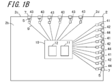
- the power supply circuit 11 is located on the second surface 2b, for example, as shown in FIG. 1B.
- the power supply circuit 11 generates a first power supply voltage VDD and a second power supply voltage VSS applied to the plurality of pixel units 4.
- the power supply circuit 11 is electrically connected to a VDD terminal 41 that outputs the first power supply voltage VDD and a VSS terminal 42 that outputs the second power supply voltage VSS.
- the first power supply voltage VDD is, for example, an anode voltage of about 10V to 15V.
- the second power supply voltage VSS is lower than the first power supply voltage VDD, and is, for example, a cathode voltage of about 0V to 3V.
- the VDD terminal 41 is led out to the first surface 2a side via the side surface wiring pad 5 and the side surface wiring 7 on the back surface side, and is electrically connected to the anode terminal of the light emitting element of the pixel portion 4 via the side surface wiring pad 5 on the front surface side.
- the VSS terminal 42 is led out to the first surface 2a side via the side surface wiring pad 5 and the side surface wiring 7 on the back surface side, and is electrically connected to the cathode terminal of the light emitting element of the pixel portion 4 via the side surface wiring pad 5 on the front surface side. Connected to.
- the scanning signal terminal 44 is arranged in the same terminal arrangement portion as the VDD terminal 41 and the VSS terminal 42.
- the scanning signal terminal 44 is electrically connected to the drive control circuit 12, is led out to the first surface 2a side via the side surface wiring pad 5 and the side surface wiring 7 on the back surface side, and is led to the first surface 2a side via the side surface wiring pad 5 on the front surface side. It is electrically connected to the gate electrode of the driving TFT of the pixel unit 4.
- FIG. 1B shows a configuration in which the VDD terminal 41, the VSS terminal 42, and the scanning signal terminal 44 form one group, and the groups are arranged in the terminal arrangement section, but the group is composed of a plurality of VDD terminals 41.
- a group consisting of a plurality of VSS terminals 42 and a group consisting of a plurality of scanning signal terminals 44 may be arranged in the terminal arrangement portion.
- the source signal terminal 43 is electrically connected to the drive control circuit 12, is led out to the first surface 2a side via the side surface wiring pad 5 and the side surface wiring 7 on the back surface side, and is led to the first surface 2a side via the side surface wiring pad 5 on the front surface side. It is electrically connected to the source electrode of the driving TFT of the pixel unit 4.
- the above-mentioned back surface drive unit 10 may include a drive control circuit 12 for controlling light emission, non-light emission, light emission intensity, and the like of the light emitting element.
- the back surface driving unit 10 may be realized by, for example, a thin film circuit formed on the second surface 2b of the substrate 2.
- the semiconductor layer constituting the thin film circuit is, for example, a semiconductor layer made of LTPS (Low Temperature Poly Silicon) directly formed on the second surface 2b by a thin film forming method such as CVD (Chemical Vapor Deposition). You may.
- the power supply circuit 11 may have an IC chip as a control circuit.
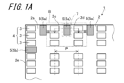
- the display device 1 includes a first side surface wiring pad 5a as a first wiring pad.
- the first side surface wiring pad 5a is connected to the side surface wiring 7 (described in FIG. 3) arranged on the side surface 2c of the substrate 2.
- the first side surface wiring pad 5a is connected to the extending portion extending to the first surface 2a of the side surface wiring 7.
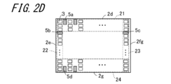
- the substrate 2 may have a rectangular shape as shown in FIGS. 1A, 1B, 2A to 2D, for example, in which case, the first side 2d and the second side 2e adjacent to the first side 2d are used.
- the first side surface wiring pad 5a is arranged on the first side 2d
- the second side surface wiring pad 5b is arranged on the second side 2e
- the third side surface wiring pad 5c is arranged on the third side 2f
- the third side surface wiring pad 5c is arranged on the fourth side 2g.
- the fourth side surface wiring pad 5d may be arranged. Therefore, when the first side surface wiring pad 5a and the like are generically referred to, they are referred to as the side surface wiring pad 5.
- the wiring pad does not necessarily have to be connected to the side wiring 7, and may be connected to a through conductor such as a through hole arranged at the edge portion of the substrate 2. Therefore, the side wiring pad 5 is one embodiment of the wiring pad. Further, the wiring pad may be a mixture of those connected to the side wiring 7 and those connected to the through conductor.
- the first side surface wiring pad 5a is located between the pixel portions 4 adjacent to each other in the direction along the first side 2d in the first outermost array portion 21 on the side of the first side 2d on the first surface 2a as the display surface. Is located in.
- a composite display device configured by connecting at least two display devices 1 by forming a portion of the side surface 2c adjacent to the first side 2d of the substrate 2 as a connecting portion to be connected to another display device 1.
- the first side surface wiring pad 5a can be used as a relay unit for a signal transmitted from the other display device 1 or a signal transmitted to the other display device 1.
- the signal may be a gate signal (scanning signal), a source signal (image signal), a power supply signal (VDD signal, VSS signal), or the like.
- the direction along the first side 2d includes a direction parallel to the first side 2d. Therefore, the direction along the first side 2d does not have to be exactly parallel to the first side 2d, and is slightly inclined with respect to the direction parallel to the first side 2d (for example, ⁇ 1 °). It may be tilted by about ⁇ 5 °).
- the distance between the first side surface wiring pad 5a and the first side 2d is 1 ⁇ 2 or less of the pixel pitch P of the plurality of pixel portions 3, and the distance from the first side surface wiring pad 5a is larger than that of the pixel portion 3 located in the first outermost array portion 21.
- the configuration may be close to the first side 2d. In the case of this configuration, when the side wiring formed by applying and firing the conductive paste is arranged on the side surface 2c adjacent to the first side 2d of the substrate 2, the conductive paste comes into contact with the pixel portion 3. It is easy to be introduced into the first side surface wiring pad 5a.
- the first side surface wiring pad 5a is provided, and the second side surface wiring pad 5b is in the second outermost array portion 22 on the side of the second side 2e in the direction along the second side 2e. It may be located between adjacent pixel portions 4.
- the portion of the side surface 2c adjacent to the first side 2d of the substrate 2 is used as a coupling portion to be coupled to the other display device 1, and the portion of the side surface 2c adjacent to the second side 2e of the substrate 2 is further used as another display device.
- a coupling portion to be coupled to 1 a composite display device configured by coupling at least three display devices 1 can be manufactured. Further, when producing a rectangular composite display device, at least four display devices 1 may be combined.
- At least four display devices 1 are coupled and configured by forming a coupling portion to be coupled to 1 and a portion of the side surface 2c adjacent to the third side 2f of the substrate 2 to be further coupled to another display device 1. It is possible to manufacture a composite display device to be used. Further, when producing a rectangular composite display device, at least six display devices 1 may be combined.
- a composite display device can be manufactured by combining at least five display devices 1 by forming a coupling portion that further combines the display device 1 with another display device 1. Further, when producing a rectangular composite display device, at least nine display devices 1 may be combined.
- the second side surface wiring pad 5b and the third side surface wiring pad 5c may not be provided.
- the portion of the side surface 2c adjacent to the first side 2d of the substrate 2 is used as a coupling portion to be coupled to the other display device 1
- the portion of the side surface 2c adjacent to the fourth side 2g of the substrate 2 is further used as another display device.
- a coupling portion to be coupled to 1 a composite display device configured by coupling at least three display devices 1 can be manufactured.
- the distance between the first side surface wiring pad 5a and the end of the substrate 2 may be 1 ⁇ 2 or less of the pixel pitch of the plurality of pixel portions 4.
- the same configuration as the above configuration of the first side surface wiring pad 5a can be adopted.
- a wall portion, a step portion, or the like made of an insulating layer higher than the upper surface of the side surface wiring pad 5a may be arranged.
- the length of the first side surface wiring pad 5a in the direction orthogonal to the first side 2d is set to the pixel portion 4 in the second outermost array portion arranged inside the first outermost array portion 21. It may be as long as it can be reached.
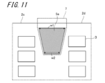
- the plan view shape of the first side surface wiring pad 5a may be a rectangular shape, a trapezoidal shape, an elliptical shape, an oval shape, or the like.
- the purpose is to prevent the conductive paste from invading the central portion side (depth direction) of the first surface 2a beyond the first side surface wiring pad 5a.
- the first side surface wiring pad 5a may be located at a position lower than the electrode pads (anode pad and cathode pad) in the pixel portion 4 (position close to the first surface 2a).
- the electrode pad in the pixel portion 4 may be located on the insulating layer on the first surface 2a, and the first side surface wiring pad 5a may not be located on the insulating layer.
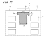
- the configuration shown in FIG. 10 is a configuration in which an extension portion 5ae extending along the first side 2d is provided at an end portion of the first side surface wiring pad 5a on the first side 2d side.
- the extending portions 5ae are provided on both sides of the end portion of the first side surface wiring pad 5a on the first side 2d side in the direction along the first side 2d, but are provided on only one side. May be good.
- FIG. 4 is a partial plan view showing a part of the display device of the other embodiments of the present disclosure in a simplified manner
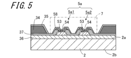
- FIG. 5 is an enlarged cross-sectional view seen from the cut plane line VV of FIG.
- the first side surface wiring pad 5a may be composed of a plurality of side surface wiring pad portions, and as shown in FIGS. 4 and 5, as the side surface wiring pad portion. It may be composed of the divided side surface wiring pad 5a1 and the divided side surface wiring pad 5a2.
- the divided side surface wiring pads 5a1 and the divided side surface wiring pads 5a2 may be arranged so as to be arranged in a direction along the first side 2d in a plan view.
- the first side surface wiring pad 5a is composed of the divided side surface wiring pad 5a1 and the divided side surface wiring pad 5a2 as in the display devices 1a of FIGS. 4 and 5, the second surface of the substrate 2 corresponds to them.
- the split side surface wiring pad on the back surface side is arranged on 2b, and the split side surface wiring pad 5a1 on the front surface side and the corresponding split side surface wiring pad on the back surface side are connected by one side surface wiring 7 and are connected to the front surface side.
- the divided side surface wiring pad 5a2 and the corresponding divided side surface wiring pad on the back surface side may be connected by another side surface wiring 7.
- the insulating layers 34 to 37 are arranged on the first surface 2a.
- the insulating layers 34 to 37 are made of, for example, an inorganic insulating layer made of SiO 2 , Si 3 N 4, or the like, or an organic insulating layer made of acrylic resin, polycarbonate, or the like.
- a switching element for controlling light emission / non-light emission of a light emitting element is not shown inside the insulating layer 36 located closest to the substrate 2 or between the substrate 2 and the insulating layer 36 among the insulating layers 34 to 37.
- a TFT or the like which is a control element for controlling the brightness, is arranged.
- the anode terminal of the ⁇ LED is electrically connected to an anode pad (not shown) which is a part of the first wiring pattern
- the cathode terminal of the ⁇ LED is an opening of the first wiring pattern. It is electrically connected to a cathode pad (not shown) formed in the portion.
- the anode pad and the cathode pad are electrically isolated from each other by an opening of a first wiring pattern formed around the anode pad.
- the cathode pad is routed around the surface of the insulating layers 34, 35 and the inner wall surface of the opening formed in the insulating layers 34, 35, and is electrically connected to the second wiring pattern.
- the surface of the anode pad and the surface of the cathode pad may be each coated with a transparent conductive layer made of indium tin oxide (ITO), indium zinc oxide (IZO), or the like.
- a conductive paste containing conductive particles such as Ag, Cu, Al, and stainless steel, an uncured resin component, an alcohol solvent, water, and the like is applied from the side surface 2c to the first surface 2a and the second surface 2b. It can be formed by a method such as a heating method, a photo-curing method in which the material is cured by irradiation with light such as ultraviolet rays, or a photo-curing heating method after the coating is applied to a desired portion of the above.
- the side wiring 7 can also be formed by a thin film forming method such as a plating method, a vapor deposition method, or a CVD method.
- a groove may be formed in advance in the portion of the side surface 2c where the side surface wiring 7 is formed. This makes it easier for the conductive paste to be the side wiring 7 to be placed at a desired portion on the side surface 2c. Further, a coating layer (overcoat layer) made of a resin material or the like may be provided to cover and protect the side wiring 7.
- the first side surface wiring pad 5 is close to the first side 2d between two pixel portions 4 adjacent to each other in the direction in which the first side 2d, which is one side of the substrate 2, extends in a plan view.
- the pixel portion 4 located in the first outermost array portion 21 is arranged, and the combined portion pixel pitch is set to the pixel pitch (non-coupling portion pixel pitch) P.
- the plurality of first side surface wiring pads 5a may all be arranged so as to be equidistant from the first side 2d.
- the frame portion around the display unit since at least a part of each first side surface wiring pad 5a is arranged inside the display unit composed of the plurality of pixel units 4 arranged in a matrix, the frame portion around the display unit. It becomes easy to make the size smaller and eliminate the frame part. As a result, when the multi-display is manufactured, it is possible to suppress the joint portion between the display devices 1 from being conspicuous, and it is possible to improve the display quality of the multi-display.
- the first side surface wiring pad 5 may be arranged at a portion close to the first side 2d and a predetermined distance from the first side 2d.
- the display device 1 has a plurality of gate signal lines and a plurality of source signal lines intersecting with the plurality of gate signal lines arranged on the first surface 2a. Further, in each pixel unit 4, a first electrode pad connected to each of a plurality of gate signal lines, a second electrode pad connected to each of a plurality of source signal lines, a first electrode pad, and a second electrode pad are provided. A thin film transistor (TFT) for driving a light emitting element, which is connected to an electrode pad, is provided. Further, although not shown, the display device 1 is electrically connected to a plurality of third electrode pads and a plurality of second electrode pads, which are electrically connected to the plurality of first electrode pads, respectively, on the second surface 2b. It has a plurality of fourth electrode pads connected to.
- TFT thin film transistor
- the plurality of first electrode pads and the plurality of third electrode pads may be electrically connected to each other via, for example, the side wiring 7.
- the plurality of second electrode pads and the plurality of fourth electrode pads may be electrically connected to each other via, for example, the side wiring 7.
- the third electrode pad is connected to a gate signal line drive circuit (gate driver) arranged on the second surface 2b via backside wiring and the like, and the fourth electrode pad is a source arranged on the second surface 2b. It may be connected to a signal line drive circuit (source driver) via backside wiring or the like.
- the gate signal line drive circuit and the source signal line drive circuit may be provided in the back surface drive unit.
- the first electrode pad and the second electrode pad provided in the pixel portions 4 in the outermost array portions 21 to 24 on the first surface 2a are at the same distance from the first side 2d to the fourth side 2g in a plan view. It may be arranged at a site separated by.
- FIG. 6 is a partial plan view showing a partially simplified display device of another embodiment of the present disclosure
- FIG. 7 is an enlarged cross-sectional view seen from the cut plane line VII-VII of FIG.
- the same reference numerals are given to the parts corresponding to the above-described embodiments.
- the portion between the first side surface wiring pad 5a and the pixel portion 4 located around the first side surface wiring pad 5a may be covered with the insulating layers 34, 35, 37. In this case, it is possible to effectively prevent the first side surface wiring pad 5a and the pixel portion 4 located around the first side surface wiring pad 5a from being short-circuited.
- the display device 1b of the present embodiment may have a recess 60 in the insulating layers 34 and 35 between the insulating layers 34 and 35 and the pixel portion 4 located around the first side surface wiring pad 5a.
- the amount of the conductive paste and the resin paste is desired. Even if the amount is larger than the amount, it is possible to prevent the recess 60 from spreading from the recess 60 to the surroundings by accumulating an excess amount in the recess 60. As a result, it is possible to prevent the conductive paste from coming into contact with the electrode pad or the like of the light emitting element.
- first side surface wiring pad 5a described above can also be applied to the second side surface wiring pad 5b, the third side surface wiring pad 5c, and the fourth side surface wiring pad 5d.
- the composite display device of the present disclosure is a composite display device configured by connecting a plurality of display devices 1 and the side surfaces of the plurality of display devices 1, and the plurality of display devices 1 are the first display devices.
- the structure may be such that the light absorber is located.
- the light absorber is formed, for example, by applying a photo-curable or thermosetting resin material containing a light-absorbing material to the first binding site and the second binding site and curing the light absorber.
- the light absorbing material may be, for example, an inorganic pigment.
- a method may be used in which a frame body having four openings is prepared, and the display device 1 is fitted and adhered to each opening.
- the composite display device 71 has a configuration in which the display devices having the configuration shown in FIG. 2 are moved in parallel, arranged at four positions, and combined.
- the pixel portions 4 arranged in the outermost array portion on the side (also referred to as the coupling side) to be coupled to the display device 1d on the first surface 2a of the substrate 2 in the display device 1c have a non-distance from the coupling side. It may be about 1/2 of the pixel pitch of the coupling portion.
- FIG. 9 is a plan view of another embodiment of the composite display device 72 of the present disclosure, and has a configuration in which four display devices 1g, 1h, 1i, and 1j (display devices having the configuration shown in FIG. 2B) are combined. be.
- the composite display device 72 arranges and connects the display devices having the configuration of FIG. 2B so that the side surfaces of the substrate 2 adjacent to the sides on the first surface 2a where the side wiring pads 5 are arranged are connected to each other. It is a configuration. In this case, it becomes easy to set the pixel pitch of the coupling portion of the pixel portions 4 arranged in the outermost array portion on the coupling side of each display device 1g to 1j to be about the same as the pixel pitch of the non-coupling portion.
- the continuity of the display image at the joint portion can be ensured, and it is possible to prevent the viewer from feeling uncomfortable with the displayed image and making it easier for the joint portion to be visually recognized.
Landscapes
- Physics & Mathematics (AREA)
- General Physics & Mathematics (AREA)
- Nonlinear Science (AREA)
- Engineering & Computer Science (AREA)
- Theoretical Computer Science (AREA)
- Chemical & Material Sciences (AREA)
- Mathematical Physics (AREA)
- Crystallography & Structural Chemistry (AREA)
- Optics & Photonics (AREA)
- Microelectronics & Electronic Packaging (AREA)
- Devices For Indicating Variable Information By Combining Individual Elements (AREA)
- Led Device Packages (AREA)
- Electroluminescent Light Sources (AREA)
Priority Applications (3)
| Application Number | Priority Date | Filing Date | Title |
|---|---|---|---|
| US17/927,633 US20230168554A1 (en) | 2020-05-26 | 2021-05-10 | Display device and composite display device |
| JP2022527638A JP7418568B2 (ja) | 2020-05-26 | 2021-05-10 | 表示装置および複合型表示装置 |
| CN202180035317.7A CN115605935A (zh) | 2020-05-26 | 2021-05-10 | 显示装置以及复合型显示装置 |
Applications Claiming Priority (2)
| Application Number | Priority Date | Filing Date | Title |
|---|---|---|---|
| JP2020091576 | 2020-05-26 | ||
| JP2020-091576 | 2020-05-26 |
Publications (1)
| Publication Number | Publication Date |
|---|---|
| WO2021241184A1 true WO2021241184A1 (ja) | 2021-12-02 |
Family
ID=78723387
Family Applications (1)
| Application Number | Title | Priority Date | Filing Date |
|---|---|---|---|
| PCT/JP2021/017672 Ceased WO2021241184A1 (ja) | 2020-05-26 | 2021-05-10 | 表示装置および複合型表示装置 |
Country Status (4)
| Country | Link |
|---|---|
| US (1) | US20230168554A1 (https=) |
| JP (1) | JP7418568B2 (https=) |
| CN (1) | CN115605935A (https=) |
| WO (1) | WO2021241184A1 (https=) |
Cited By (3)
| Publication number | Priority date | Publication date | Assignee | Title |
|---|---|---|---|---|
| CN114447183A (zh) * | 2021-12-08 | 2022-05-06 | 友达光电股份有限公司 | 显示模块 |
| CN116387321A (zh) * | 2021-12-31 | 2023-07-04 | 乐金显示有限公司 | 发光显示设备 |
| JP2024095958A (ja) * | 2022-12-30 | 2024-07-11 | エルジー ディスプレイ カンパニー リミテッド | 表示装置 |
Families Citing this family (4)
| Publication number | Priority date | Publication date | Assignee | Title |
|---|---|---|---|---|
| KR102943784B1 (ko) * | 2020-09-28 | 2026-03-24 | 엘지디스플레이 주식회사 | 표시 장치 및 다중 패널 표시 장치 |
| KR20220096921A (ko) * | 2020-12-31 | 2022-07-07 | 엘지디스플레이 주식회사 | 발광 표시 장치와 이를 이용한 멀티 스크린 발광 표시 장치 |
| JP7594196B2 (ja) * | 2022-08-01 | 2024-12-04 | 日亜化学工業株式会社 | 発光装置 |
| US20260023284A1 (en) * | 2023-11-15 | 2026-01-22 | BOE MLED Technology Co., Ltd. | Wiring Substrate, Mask Assembly, Backplane, and Display Device |
Citations (6)
| Publication number | Priority date | Publication date | Assignee | Title |
|---|---|---|---|---|
| US20080030124A1 (en) * | 2006-08-03 | 2008-02-07 | Kyung-Sun Ryu | Light emission device and display device |
| JP2009042758A (ja) * | 2007-08-06 | 2009-02-26 | Barco Nv | タイル状ディスプレイ、タイル状ディスプレイシステム、ディスプレイタイル、ならびに、タイル状ディスプレイを組立てるため、および調節するための方法 |
| US20180190631A1 (en) * | 2016-12-30 | 2018-07-05 | Lg Display Co., Ltd. | Display device and multi-screen display device using the same |
| US20180323180A1 (en) * | 2017-05-05 | 2018-11-08 | X-Celeprint Limited | Matrix-addressed tiles and arrays |
| WO2019045549A1 (ko) * | 2017-09-04 | 2019-03-07 | 서울반도체주식회사 | 표시 장치 및 그의 제조 방법 |
| US20190122592A1 (en) * | 2017-10-25 | 2019-04-25 | Samsung Electronics Co., Ltd. | Led panel and display apparatus having the same |
Family Cites Families (7)
| Publication number | Priority date | Publication date | Assignee | Title |
|---|---|---|---|---|
| WO2005031450A1 (en) * | 2003-09-29 | 2005-04-07 | Koninklijke Philips Electronics, N.V. | Electronic paint with charge memory |
| JP2010231931A (ja) * | 2009-03-26 | 2010-10-14 | Casio Computer Co Ltd | 発光装置及びその製造方法 |
| JP2010278318A (ja) * | 2009-05-29 | 2010-12-09 | Renesas Electronics Corp | 半導体装置 |
| KR102379591B1 (ko) * | 2014-04-10 | 2022-03-30 | 삼성디스플레이 주식회사 | 전자부품, 이를 포함하는 전자기기 및 전자기기의 본딩 방법 |
| US9477438B1 (en) * | 2015-09-25 | 2016-10-25 | Revolution Display, Llc | Devices for creating mosaicked display systems, and display mosaic systems comprising same |
| JP6856472B2 (ja) * | 2017-07-31 | 2021-04-07 | 京セラ株式会社 | 表示装置 |
| CN107809843B (zh) * | 2017-11-30 | 2019-12-20 | 武汉天马微电子有限公司 | 一种绑定部件、显示基板及显示面板 |
-
2021
- 2021-05-10 WO PCT/JP2021/017672 patent/WO2021241184A1/ja not_active Ceased
- 2021-05-10 US US17/927,633 patent/US20230168554A1/en not_active Abandoned
- 2021-05-10 JP JP2022527638A patent/JP7418568B2/ja active Active
- 2021-05-10 CN CN202180035317.7A patent/CN115605935A/zh active Pending
Patent Citations (6)
| Publication number | Priority date | Publication date | Assignee | Title |
|---|---|---|---|---|
| US20080030124A1 (en) * | 2006-08-03 | 2008-02-07 | Kyung-Sun Ryu | Light emission device and display device |
| JP2009042758A (ja) * | 2007-08-06 | 2009-02-26 | Barco Nv | タイル状ディスプレイ、タイル状ディスプレイシステム、ディスプレイタイル、ならびに、タイル状ディスプレイを組立てるため、および調節するための方法 |
| US20180190631A1 (en) * | 2016-12-30 | 2018-07-05 | Lg Display Co., Ltd. | Display device and multi-screen display device using the same |
| US20180323180A1 (en) * | 2017-05-05 | 2018-11-08 | X-Celeprint Limited | Matrix-addressed tiles and arrays |
| WO2019045549A1 (ko) * | 2017-09-04 | 2019-03-07 | 서울반도체주식회사 | 표시 장치 및 그의 제조 방법 |
| US20190122592A1 (en) * | 2017-10-25 | 2019-04-25 | Samsung Electronics Co., Ltd. | Led panel and display apparatus having the same |
Cited By (4)
| Publication number | Priority date | Publication date | Assignee | Title |
|---|---|---|---|---|
| CN114447183A (zh) * | 2021-12-08 | 2022-05-06 | 友达光电股份有限公司 | 显示模块 |
| CN116387321A (zh) * | 2021-12-31 | 2023-07-04 | 乐金显示有限公司 | 发光显示设备 |
| JP2024095958A (ja) * | 2022-12-30 | 2024-07-11 | エルジー ディスプレイ カンパニー リミテッド | 表示装置 |
| JP7542699B2 (ja) | 2022-12-30 | 2024-08-30 | エルジー ディスプレイ カンパニー リミテッド | 表示装置 |
Also Published As
| Publication number | Publication date |
|---|---|
| JPWO2021241184A1 (https=) | 2021-12-02 |
| CN115605935A (zh) | 2023-01-13 |
| US20230168554A1 (en) | 2023-06-01 |
| JP7418568B2 (ja) | 2024-01-19 |
Similar Documents
| Publication | Publication Date | Title |
|---|---|---|
| JP7418568B2 (ja) | 表示装置および複合型表示装置 | |
| US10943969B2 (en) | Multi-panel organic light emitting display device | |
| JP7047889B2 (ja) | 表示装置及び電子機器 | |
| KR102151099B1 (ko) | 디스플레이 패널 및 이를 이용한 대형 디스플레이 장치 | |
| TWI707326B (zh) | 顯示裝置 | |
| CN113661580B (zh) | 微型led元件基板以及显示装置 | |
| EP3343628B1 (en) | Organic light emitting display device and method of manufacturing thereof | |
| CN114746928B (zh) | 显示装置 | |
| WO2017169268A1 (ja) | 表示装置及び電子機器 | |
| JP7311595B2 (ja) | 発光素子基板および表示装置、ならびに表示装置の製造方法 | |
| JP7466701B2 (ja) | 表示装置および表示装置の製造方法 | |
| WO2020189131A1 (ja) | 表示装置 | |
| JP7326470B2 (ja) | 表示装置 | |
| CN114267683B (zh) | 一种显示背板及其制备方法、显示装置 | |
| JP7325547B2 (ja) | 表示装置および表示装置の製造方法 | |
| JP7418590B2 (ja) | 表示装置 | |
| US20220165812A1 (en) | Light emitting display panel and light emitting display device including the same | |
| US20240038954A1 (en) | Display device and composite display device | |
| JP2022098894A (ja) | 表示装置及びその製造方法 | |
| JP2022098885A (ja) | 表示装置及びその製造方法 | |
| JP2022098887A (ja) | マルチディスプレイ | |
| JP2022038445A (ja) | 遮光層積層型基板 | |
| KR102428392B1 (ko) | 유기발광 표시장치 | |
| WO2023008243A1 (ja) | 画素構造体および表示装置 | |
| WO2024232324A1 (ja) | 合わせ透明板及びその製造方法 |
Legal Events
| Date | Code | Title | Description |
|---|---|---|---|
| 121 | Ep: the epo has been informed by wipo that ep was designated in this application |
Ref document number: 21813141 Country of ref document: EP Kind code of ref document: A1 |
|
| ENP | Entry into the national phase |
Ref document number: 2022527638 Country of ref document: JP Kind code of ref document: A |
|
| NENP | Non-entry into the national phase |
Ref country code: DE |
|
| 122 | Ep: pct application non-entry in european phase |
Ref document number: 21813141 Country of ref document: EP Kind code of ref document: A1 |