WO2021234983A1 - 光学装置 - Google Patents
光学装置 Download PDFInfo
- Publication number
- WO2021234983A1 WO2021234983A1 PCT/JP2020/044344 JP2020044344W WO2021234983A1 WO 2021234983 A1 WO2021234983 A1 WO 2021234983A1 JP 2020044344 W JP2020044344 W JP 2020044344W WO 2021234983 A1 WO2021234983 A1 WO 2021234983A1
- Authority
- WO
- WIPO (PCT)
- Prior art keywords
- light
- light emitting
- emitting element
- scanning
- scanning element
- Prior art date
- Legal status (The legal status is an assumption and is not a legal conclusion. Google has not performed a legal analysis and makes no representation as to the accuracy of the status listed.)
- Ceased
Links
Images


Classifications
-
- G—PHYSICS
- G02—OPTICS
- G02B—OPTICAL ELEMENTS, SYSTEMS OR APPARATUS
- G02B26/00—Optical devices or arrangements for the control of light using movable or deformable optical elements
- G02B26/08—Optical devices or arrangements for the control of light using movable or deformable optical elements for controlling the direction of light
- G02B26/0816—Optical devices or arrangements for the control of light using movable or deformable optical elements for controlling the direction of light by means of one or more reflecting elements
-
- G—PHYSICS
- G02—OPTICS
- G02B—OPTICAL ELEMENTS, SYSTEMS OR APPARATUS
- G02B17/00—Systems with reflecting surfaces, with or without refracting elements
- G02B17/08—Catadioptric systems
- G02B17/0856—Catadioptric systems comprising a refractive element with a reflective surface, the reflection taking place inside the element, e.g. Mangin mirrors
- G02B17/086—Catadioptric systems comprising a refractive element with a reflective surface, the reflection taking place inside the element, e.g. Mangin mirrors wherein the system is made of a single block of optical material, e.g. solid catadioptric systems
-
- G—PHYSICS
- G02—OPTICS
- G02B—OPTICAL ELEMENTS, SYSTEMS OR APPARATUS
- G02B26/00—Optical devices or arrangements for the control of light using movable or deformable optical elements
- G02B26/08—Optical devices or arrangements for the control of light using movable or deformable optical elements for controlling the direction of light
- G02B26/10—Scanning systems
- G02B26/101—Scanning systems with both horizontal and vertical deflecting means, e.g. raster or XY scanners
-
- G—PHYSICS
- G02—OPTICS
- G02B—OPTICAL ELEMENTS, SYSTEMS OR APPARATUS
- G02B27/00—Optical systems or apparatus not provided for by any of the groups G02B1/00 - G02B26/00, G02B30/00
- G02B27/10—Beam splitting or combining systems
-
- G—PHYSICS
- G02—OPTICS
- G02B—OPTICAL ELEMENTS, SYSTEMS OR APPARATUS
- G02B5/00—Optical elements other than lenses
- G02B5/04—Prisms
-
- G—PHYSICS
- G02—OPTICS
- G02B—OPTICAL ELEMENTS, SYSTEMS OR APPARATUS
- G02B5/00—Optical elements other than lenses
- G02B5/08—Mirrors
- G02B5/10—Mirrors with curved faces
Definitions
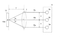
- FIG. 1 is a configuration diagram showing the configuration of the optical device 1 according to the present disclosure.
- the optical device 1 includes an optical system 3 and a control unit 21.
- the optical system 3 includes a light emitting element group 5, a lens element 7, a first scanning element 13, a prism 15, and a second scanning element 17.
- the prism 15 is a form of a relay optical system that collects the light R scanned by the first scanning element 13 in the second scanning element 17 between the optical paths from the first scanning element 13 to the second scanning element 17.
- the prism 15 has an incident surface 15a and an emitting surface 15d, and further has one or more reflecting surfaces between the optical paths from the incident surface 15a to the emitting surface 15d. In this embodiment, for example, it has a first reflecting surface 15b and a second reflecting surface 15c.
- the entrance surface 15a and the exit surface 15d have a flat plate shape, a convex shape, or a concave shape.
- the prism 15 is made of, for example, resin or glass.
- the relay optical system may be composed of a plurality of reflection mirrors, but by adopting a prism as the relay optical system, the size of the relay optical system can be reduced.
- the lens element 7, the first scanning element 13, the incident surface 15a of the prism 15, the first reflecting surface 15b of the prism 15, and the prism are arranged in the order of the optical path from the light emitting element group 5.
- the second reflecting surface 15c of 15, the exit surface 15d of the prism 15, and the second scanning element 17 are arranged. Therefore, the prism 15 is arranged between the optical paths from the first scanning element 13 to the second scanning element 17.
- the first scanning element 13 is driven by the control unit 21 with the time of returning from t0 through t8 to t0 as one cycle. Therefore, in the drawing area Ap, an image in which blue, green, and red colors are combined can be displayed, in the red area Aa, only a red image can be displayed, and in the green + red area Aba, green and red are displayed. It is possible to display an image that combines the respective colored lights of. Further, in the blue region Ac, only a blue image can be displayed, and in the green + blue region Abc, an image in which the respective colored lights of green and blue are combined can be displayed.
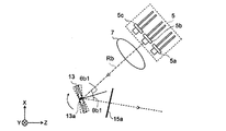
- the light emitting elements 5a to 5c are emitted at the timings at which they can be combined, and the light Ra, Rb, and Rc are reflected by the first scanning element 13 in the same direction with a time lag, so that the light is apparently matched. Be waved.
- Each light Ra, Rb, and Rc reflected in the same direction travels in the prism 15, is scanned by the second scanning element 17, and is incident on the same position on the projection surface 19.
- the same direction includes a deviation in a direction in which each light projected on the projection surface 19 can be recognized by a person as being synthesized.
- the first scanning element 13 rotates clockwise, the light emitting element 5b emits light at the timing of t4, and the green light Rb is second incident on the first scanning element 13. It is incident at the incident angle ⁇ b1 as an angle, is reflected at the reflected angle ⁇ b1, and is directed toward the incident surface 15a in the same direction as the blue light Rc is reflected.
- each light Ra, Rb, Rc can be reflected in the same direction, and each light Ra, Rb, Rc can be synthesized.
- the light emitting elements 5a, 5b, and 5c are arranged at equal intervals, but they may be arranged at different intervals.
- FIGS. 4 to 6 the incident angles of the light emitting element group 5 and the first scanning element 13 when correcting the incident angle of the projection surface 19 to a predetermined position are shown by ⁇ a1, ⁇ b1, and ⁇ c1, but the projection surface. ⁇ a1, ⁇ b1, and ⁇ c1 change according to the predetermined position of.
- the optical device 1 of the first embodiment includes a light emitting element group 5 having a light emitting element 5a and a light emitting element 5b, a red light Ra emitted from the light emitting element 5a, and a green light Rb emitted from the light emitting element 5b.
- a lens element 7 for condensing light at a predetermined position is provided.
- the optical device 1 is arranged at a predetermined position, and the light Ra and the light Rb emitted from the lens element 7 emit light from the first scanning element 13, the light emitting element 5a, and the light emitting element 5b, respectively, in which the light Ra and the light Rb are incident at different angles.
- a control unit 21 for controlling light emission by shifting the timing is provided.
- the incident angle ⁇ a1 of the red light Ra to the first scanning element 13 is smaller than the incident angle ⁇ b2 of the green light Rb.
- the first scanning element 13A rotates around a scanning axis 13Aa that intersects the plane PL2, and scans the incident light in the plane PL2 in the Y direction.
- the first scanning element 13A is, for example, a mirror that is rotationally driven with the X direction as a rotation axis (scanning axis 13Aa) by piezoelectric drive.
- the first scanning element 13A is, for example, a horizontal scanner.
- the light reflected by the first scanning element 13A is diffused in the Y direction. Since each light incident on the first scanning element 13A from the light emitting elements 5a to 5c has an incident angle with respect to the X direction, the light incident on the first scanning element 13A is reflected in the negative direction of X. It is incident on the prism 15.
- the light emitting elements 5a, 5b, and 5c are arranged side by side in the Y direction, for example. As long as it is in the plane PL2, it may be arranged so as to be displaced in the front-rear direction with respect to the light emission direction.
- the light emitting element 5c emits light at the timing of t3, the blue light Rc is incident on the first scanning element 13A at the incident angle ⁇ c2, and is reflected at the reflection angle ⁇ c2 to be reflected on the incident surface. Head to 15a.
- one lens element 7 is arranged for the three light emitting elements 5a, 5b, and 5c, but the present invention is not limited to this.
- the optical system 3 may have a plurality of lens elements 7a, and one lens element 7a may be arranged for one light emitting element.
- the lens element 7a is, for example, a collimating lens.
- the light emitting element group has a third light emitting element, and the lens element is incident with the third light emitted from the third light emitting element.
- the control unit includes the first light emitting element, the second light emitting element, and the third light emitting element.
- the light emission control is performed by shifting the light emission timing of each, and the first light emitting element and the second light emitting element are included in the same plane so that the optical axis of the first light, the optical axis of the second light, and the optical axis of the third light are included in the same plane.
- the optical device of (8) includes a relay optical system that collects the light scanned by the first scanning element in the second scanning element between the optical paths from the first scanning element to the second scanning element. ..
Landscapes
- Physics & Mathematics (AREA)
- General Physics & Mathematics (AREA)
- Optics & Photonics (AREA)
- Mechanical Optical Scanning Systems (AREA)
Priority Applications (2)
| Application Number | Priority Date | Filing Date | Title |
|---|---|---|---|
| JP2022524867A JP7634188B2 (ja) | 2020-05-19 | 2020-11-27 | 光学装置 |
| US17/988,968 US20230085385A1 (en) | 2020-05-19 | 2022-11-17 | Optical device |
Applications Claiming Priority (2)
| Application Number | Priority Date | Filing Date | Title |
|---|---|---|---|
| JP2020-087487 | 2020-05-19 | ||
| JP2020087487 | 2020-05-19 |
Related Child Applications (1)
| Application Number | Title | Priority Date | Filing Date |
|---|---|---|---|
| US17/988,968 Continuation US20230085385A1 (en) | 2020-05-19 | 2022-11-17 | Optical device |
Publications (1)
| Publication Number | Publication Date |
|---|---|
| WO2021234983A1 true WO2021234983A1 (ja) | 2021-11-25 |
Family
ID=78708371
Family Applications (1)
| Application Number | Title | Priority Date | Filing Date |
|---|---|---|---|
| PCT/JP2020/044344 Ceased WO2021234983A1 (ja) | 2020-05-19 | 2020-11-27 | 光学装置 |
Country Status (3)
| Country | Link |
|---|---|
| US (1) | US20230085385A1 (https=) |
| JP (1) | JP7634188B2 (https=) |
| WO (1) | WO2021234983A1 (https=) |
Citations (1)
| Publication number | Priority date | Publication date | Assignee | Title |
|---|---|---|---|---|
| JP2015215443A (ja) * | 2014-05-09 | 2015-12-03 | シチズンホールディングス株式会社 | 投影装置 |
Family Cites Families (5)
| Publication number | Priority date | Publication date | Assignee | Title |
|---|---|---|---|---|
| US7273281B2 (en) | 2003-12-31 | 2007-09-25 | Symbol Technologies, Inc. | Method and apparatus for aligning a plurality of lasers in an electronic display device |
| JP4857582B2 (ja) * | 2005-03-30 | 2012-01-18 | ブラザー工業株式会社 | 光走査装置および光走査装置の制御方法 |
| JP2007178942A (ja) | 2005-12-28 | 2007-07-12 | Brother Ind Ltd | 光走査装置、画像表示装置及び網膜走査型画像表示装置 |
| JP2007140010A (ja) | 2005-11-17 | 2007-06-07 | Seiko Epson Corp | 画像表示装置 |
| US9438871B2 (en) | 2012-12-26 | 2016-09-06 | Citizen Holdings Co., Ltd. | Laser projection apparatus with bundled fibers |
-
2020
- 2020-11-27 WO PCT/JP2020/044344 patent/WO2021234983A1/ja not_active Ceased
- 2020-11-27 JP JP2022524867A patent/JP7634188B2/ja active Active
-
2022
- 2022-11-17 US US17/988,968 patent/US20230085385A1/en active Pending
Patent Citations (1)
| Publication number | Priority date | Publication date | Assignee | Title |
|---|---|---|---|---|
| JP2015215443A (ja) * | 2014-05-09 | 2015-12-03 | シチズンホールディングス株式会社 | 投影装置 |
Also Published As
| Publication number | Publication date |
|---|---|
| JPWO2021234983A1 (https=) | 2021-11-25 |
| US20230085385A1 (en) | 2023-03-16 |
| JP7634188B2 (ja) | 2025-02-21 |
Similar Documents
| Publication | Publication Date | Title |
|---|---|---|
| US12088970B2 (en) | Light source device and projection display apparatus | |
| JP5954845B2 (ja) | 照明光学系、照明光学系の色むら改善方法、プロジェクターおよびプロジェクターシステム | |
| US8746892B2 (en) | Illuminating optical system and projector device | |
| US10914876B2 (en) | Light source device and projection display apparatus | |
| CN107436528A (zh) | 光源装置和投影仪 | |
| CN101874221B (zh) | 光学扫描装置和图像输出设备 | |
| JP2013041236A (ja) | 走査型画像表示装置及び走査型投影装置 | |
| CN112731749B (zh) | 激光投影设备 | |
| US10690931B2 (en) | Light source device and projection display apparatus | |
| JP4353287B2 (ja) | プロジェクタ | |
| WO2020218035A1 (ja) | 光学系 | |
| JP2018159837A (ja) | 光源装置および投射型表示装置 | |
| JP7236642B2 (ja) | 光源装置及び投写型映像表示装置 | |
| JP2007047245A (ja) | 光源装置、光走査装置及び画像表示装置 | |
| JP2019207394A (ja) | 光源装置及び投写型映像表示装置 | |
| JP4166493B2 (ja) | マルチビーム走査装置および光源装置 | |
| WO2021234983A1 (ja) | 光学装置 | |
| JP2016180818A (ja) | 照明光学系及びこれを用いた投射型表示装置 | |
| CN113260899B (zh) | 光学系统 | |
| CN103576313A (zh) | 光束扫描装置以及光束扫描型图像放映装置 | |
| US12541142B2 (en) | Light source device and projection device | |
| US20250271738A1 (en) | Light source system and projection device | |
| CN112738484B (zh) | 激光投影设备 | |
| JP2019101200A (ja) | 光源装置および投写型映像表示装置 | |
| JP2006292792A (ja) | 光投射装置及びプロジェクタ |
Legal Events
| Date | Code | Title | Description |
|---|---|---|---|
| 121 | Ep: the epo has been informed by wipo that ep was designated in this application |
Ref document number: 20936083 Country of ref document: EP Kind code of ref document: A1 |
|
| ENP | Entry into the national phase |
Ref document number: 2022524867 Country of ref document: JP Kind code of ref document: A |
|
| NENP | Non-entry into the national phase |
Ref country code: DE |
|
| 122 | Ep: pct application non-entry in european phase |
Ref document number: 20936083 Country of ref document: EP Kind code of ref document: A1 |