WO2021234983A1 - Optical device - Google Patents
Optical device Download PDFInfo
- Publication number
- WO2021234983A1 WO2021234983A1 PCT/JP2020/044344 JP2020044344W WO2021234983A1 WO 2021234983 A1 WO2021234983 A1 WO 2021234983A1 JP 2020044344 W JP2020044344 W JP 2020044344W WO 2021234983 A1 WO2021234983 A1 WO 2021234983A1
- Authority
- WO
- WIPO (PCT)
- Prior art keywords
- light
- light emitting
- emitting element
- scanning
- scanning element
- Prior art date
Links
Images


Classifications
-
- G—PHYSICS
- G02—OPTICS
- G02B—OPTICAL ELEMENTS, SYSTEMS OR APPARATUS
- G02B26/00—Optical devices or arrangements for the control of light using movable or deformable optical elements
- G02B26/08—Optical devices or arrangements for the control of light using movable or deformable optical elements for controlling the direction of light
- G02B26/0816—Optical devices or arrangements for the control of light using movable or deformable optical elements for controlling the direction of light by means of one or more reflecting elements
-
- G—PHYSICS
- G02—OPTICS
- G02B—OPTICAL ELEMENTS, SYSTEMS OR APPARATUS
- G02B17/00—Systems with reflecting surfaces, with or without refracting elements
- G02B17/08—Catadioptric systems
- G02B17/0856—Catadioptric systems comprising a refractive element with a reflective surface, the reflection taking place inside the element, e.g. Mangin mirrors
- G02B17/086—Catadioptric systems comprising a refractive element with a reflective surface, the reflection taking place inside the element, e.g. Mangin mirrors wherein the system is made of a single block of optical material, e.g. solid catadioptric systems
-
- G—PHYSICS
- G02—OPTICS
- G02B—OPTICAL ELEMENTS, SYSTEMS OR APPARATUS
- G02B26/00—Optical devices or arrangements for the control of light using movable or deformable optical elements
- G02B26/08—Optical devices or arrangements for the control of light using movable or deformable optical elements for controlling the direction of light
- G02B26/10—Scanning systems
- G02B26/101—Scanning systems with both horizontal and vertical deflecting means, e.g. raster or XY scanners
-
- G—PHYSICS
- G02—OPTICS
- G02B—OPTICAL ELEMENTS, SYSTEMS OR APPARATUS
- G02B27/00—Optical systems or apparatus not provided for by any of the groups G02B1/00 - G02B26/00, G02B30/00
- G02B27/10—Beam splitting or combining systems
-
- G—PHYSICS
- G02—OPTICS
- G02B—OPTICAL ELEMENTS, SYSTEMS OR APPARATUS
- G02B5/00—Optical elements other than lenses
- G02B5/04—Prisms
-
- G—PHYSICS
- G02—OPTICS
- G02B—OPTICAL ELEMENTS, SYSTEMS OR APPARATUS
- G02B5/00—Optical elements other than lenses
- G02B5/08—Mirrors
- G02B5/10—Mirrors with curved faces
Definitions
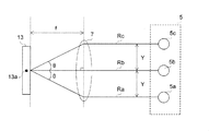
- FIG. 1 is a configuration diagram showing the configuration of the optical device 1 according to the present disclosure.
- the optical device 1 includes an optical system 3 and a control unit 21.
- the optical system 3 includes a light emitting element group 5, a lens element 7, a first scanning element 13, a prism 15, and a second scanning element 17.
- the prism 15 is a form of a relay optical system that collects the light R scanned by the first scanning element 13 in the second scanning element 17 between the optical paths from the first scanning element 13 to the second scanning element 17.
- the prism 15 has an incident surface 15a and an emitting surface 15d, and further has one or more reflecting surfaces between the optical paths from the incident surface 15a to the emitting surface 15d. In this embodiment, for example, it has a first reflecting surface 15b and a second reflecting surface 15c.
- the entrance surface 15a and the exit surface 15d have a flat plate shape, a convex shape, or a concave shape.
- the prism 15 is made of, for example, resin or glass.
- the relay optical system may be composed of a plurality of reflection mirrors, but by adopting a prism as the relay optical system, the size of the relay optical system can be reduced.
- the lens element 7, the first scanning element 13, the incident surface 15a of the prism 15, the first reflecting surface 15b of the prism 15, and the prism are arranged in the order of the optical path from the light emitting element group 5.
- the second reflecting surface 15c of 15, the exit surface 15d of the prism 15, and the second scanning element 17 are arranged. Therefore, the prism 15 is arranged between the optical paths from the first scanning element 13 to the second scanning element 17.
- the first scanning element 13 is driven by the control unit 21 with the time of returning from t0 through t8 to t0 as one cycle. Therefore, in the drawing area Ap, an image in which blue, green, and red colors are combined can be displayed, in the red area Aa, only a red image can be displayed, and in the green + red area Aba, green and red are displayed. It is possible to display an image that combines the respective colored lights of. Further, in the blue region Ac, only a blue image can be displayed, and in the green + blue region Abc, an image in which the respective colored lights of green and blue are combined can be displayed.
- the light emitting elements 5a to 5c are emitted at the timings at which they can be combined, and the light Ra, Rb, and Rc are reflected by the first scanning element 13 in the same direction with a time lag, so that the light is apparently matched. Be waved.
- Each light Ra, Rb, and Rc reflected in the same direction travels in the prism 15, is scanned by the second scanning element 17, and is incident on the same position on the projection surface 19.
- the same direction includes a deviation in a direction in which each light projected on the projection surface 19 can be recognized by a person as being synthesized.
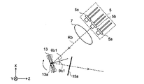
- the first scanning element 13 rotates clockwise, the light emitting element 5b emits light at the timing of t4, and the green light Rb is second incident on the first scanning element 13. It is incident at the incident angle ⁇ b1 as an angle, is reflected at the reflected angle ⁇ b1, and is directed toward the incident surface 15a in the same direction as the blue light Rc is reflected.
- each light Ra, Rb, Rc can be reflected in the same direction, and each light Ra, Rb, Rc can be synthesized.
- the light emitting elements 5a, 5b, and 5c are arranged at equal intervals, but they may be arranged at different intervals.
- FIGS. 4 to 6 the incident angles of the light emitting element group 5 and the first scanning element 13 when correcting the incident angle of the projection surface 19 to a predetermined position are shown by ⁇ a1, ⁇ b1, and ⁇ c1, but the projection surface. ⁇ a1, ⁇ b1, and ⁇ c1 change according to the predetermined position of.
- the optical device 1 of the first embodiment includes a light emitting element group 5 having a light emitting element 5a and a light emitting element 5b, a red light Ra emitted from the light emitting element 5a, and a green light Rb emitted from the light emitting element 5b.
- a lens element 7 for condensing light at a predetermined position is provided.
- the optical device 1 is arranged at a predetermined position, and the light Ra and the light Rb emitted from the lens element 7 emit light from the first scanning element 13, the light emitting element 5a, and the light emitting element 5b, respectively, in which the light Ra and the light Rb are incident at different angles.
- a control unit 21 for controlling light emission by shifting the timing is provided.
- the incident angle ⁇ a1 of the red light Ra to the first scanning element 13 is smaller than the incident angle ⁇ b2 of the green light Rb.
- the first scanning element 13A rotates around a scanning axis 13Aa that intersects the plane PL2, and scans the incident light in the plane PL2 in the Y direction.
- the first scanning element 13A is, for example, a mirror that is rotationally driven with the X direction as a rotation axis (scanning axis 13Aa) by piezoelectric drive.
- the first scanning element 13A is, for example, a horizontal scanner.
- the light reflected by the first scanning element 13A is diffused in the Y direction. Since each light incident on the first scanning element 13A from the light emitting elements 5a to 5c has an incident angle with respect to the X direction, the light incident on the first scanning element 13A is reflected in the negative direction of X. It is incident on the prism 15.
- the light emitting elements 5a, 5b, and 5c are arranged side by side in the Y direction, for example. As long as it is in the plane PL2, it may be arranged so as to be displaced in the front-rear direction with respect to the light emission direction.
- the light emitting element 5c emits light at the timing of t3, the blue light Rc is incident on the first scanning element 13A at the incident angle ⁇ c2, and is reflected at the reflection angle ⁇ c2 to be reflected on the incident surface. Head to 15a.
- one lens element 7 is arranged for the three light emitting elements 5a, 5b, and 5c, but the present invention is not limited to this.
- the optical system 3 may have a plurality of lens elements 7a, and one lens element 7a may be arranged for one light emitting element.
- the lens element 7a is, for example, a collimating lens.
- the light emitting element group has a third light emitting element, and the lens element is incident with the third light emitted from the third light emitting element.
- the control unit includes the first light emitting element, the second light emitting element, and the third light emitting element.
- the light emission control is performed by shifting the light emission timing of each, and the first light emitting element and the second light emitting element are included in the same plane so that the optical axis of the first light, the optical axis of the second light, and the optical axis of the third light are included in the same plane.
- the optical device of (8) includes a relay optical system that collects the light scanned by the first scanning element in the second scanning element between the optical paths from the first scanning element to the second scanning element. ..
Abstract
The present invention provides an optical device comprising a lens element that condenses first light emitted from a first light-emitting element and second light emitted from a second light-emitting element onto a predetermined position, a first scanning element that is disposed at the predetermined position and causes the first light and the second light emitted from the lens element to enter at respectively different angles, and a control unit that controls light emission by shifting the light emission timing of the first light-emitting element and the light emission timing of the second light-emitting element from each other, wherein the first light-emitting element and the second light-emitting element are arranged such that the optical axis of the first light and the optical axis of the second light lie in the same plane, and the control unit controls the light emission timings of the first light-emitting element and the second light-emitting element in correspondence with the rotation of the first scanning element such that the first light and the second light are reflected in the same direction by the first scanning element, respectively.
Description
本開示は、複数の光を合波する光学装置に関する。
The present disclosure relates to an optical device that combines a plurality of lights.
特許文献1は、レーザ光を2方向にそれぞれ走査する走査装置を有する光学系を開示する。この光学系は、走査されたレーザ光をミラーを用いて伝送することが記載されている。また、光源から1つの光が伝送されている。
Patent Document 1 discloses an optical system having a scanning device that scans a laser beam in two directions, respectively. It is described that this optical system transmits a scanned laser beam using a mirror. Further, one light is transmitted from the light source.
しかしながら、特許文献1の光源は1つであり、複数の光源からの光を合波する場合、合波素子が必要になる。例えば、ダイクロイックミラーのような合波素子を光学系が備える必要があり、この場合、光学系が大型化する問題がある。
However, the light source of Patent Document 1 is one, and when light from a plurality of light sources is combined, a wave combining element is required. For example, it is necessary for the optical system to include a combiner element such as a dichroic mirror, and in this case, there is a problem that the optical system becomes large.
本開示は、光学系の大型化を抑制し、複数の光源からの光を合波する光学装置を提供する。
The present disclosure provides an optical device that suppresses an increase in the size of an optical system and combines light from a plurality of light sources.
本開示の光学装置は、第1発光素子と第2発光素子とを有する発光素子群と、第1発光素子から出射された第1光と第2発光素子から出射された第2光とを所定の位置に導くレンズ素子と、所定の位置に配置され、レンズ素子から出射した第1光および第2光が、それぞれ、互いに異なる角度で入射する第1走査素子と、第1発光素子と第2発光素子との発光タイミングをずらして発光制御する制御部と、第1光の光軸と第2光の光軸とが同一平面内に含まれるように第1発光素子と第2発光素子とが配列されており、第1走査素子は、平面と直交する方向の走査軸を有し、走査軸を中心に回転し、制御部は、第1光及び第2光がそれぞれ第1走査素子により同じ方向へ反射されるように、第1走査素子の回転に対応して第1発光素子と第2発光素子との発光タイミングを制御する。
The optical device of the present disclosure defines a group of light emitting elements having a first light emitting element and a second light emitting element, and a first light emitted from the first light emitting element and a second light emitted from the second light emitting element. The first scanning element, the first light emitting element, and the second light emitting element, which are arranged at a predetermined position and the first light and the second light emitted from the lens element are incident at different angles from each other. The control unit that controls light emission by shifting the light emission timing from the light emitting element, and the first light emitting element and the second light emitting element so that the optical axis of the first light and the optical axis of the second light are included in the same plane. The first scanning element has a scanning axis in a direction orthogonal to the plane and rotates about the scanning axis, and the control unit has the same first light and second light by the first scanning element, respectively. The light emission timing between the first light emitting element and the second light emitting element is controlled in response to the rotation of the first scanning element so that the light is reflected in the direction.
本開示における光学装置によれば、光学系の大型化を抑制し、複数の光源からの光を合波することが可能である。
According to the optical device in the present disclosure, it is possible to suppress the enlargement of the optical system and combine the light from a plurality of light sources.
以下、適宜図面を参照しながら、実施の形態を詳細に説明する。但し、必要以上に詳細な説明は省略する場合がある。例えば、既によく知られた事項の詳細説明や実質的に同一の構成に対する重複説明を省略する場合がある。これは、以下の説明が不必要に冗長になるのを避け、当業者の理解を容易にするためである。
なお、発明者(ら)は、当業者が本開示を十分に理解するために添付図面および以下の説明を提供するのであって、これらによって特許請求の範囲に記載の主題を限定することを意図するものではない。 Hereinafter, embodiments will be described in detail with reference to the drawings as appropriate. However, more detailed explanation than necessary may be omitted. For example, detailed explanations of already well-known matters and duplicate explanations for substantially the same configuration may be omitted. This is to avoid unnecessary redundancy of the following description and to facilitate the understanding of those skilled in the art.
It should be noted that the inventor (or others) intends to limit the subject matter described in the claims by those skilled in the art by providing the accompanying drawings and the following description in order to fully understand the present disclosure. It's not something to do.
(第1実施形態)
以下、図1~図6を用いて、第1実施形態を説明する。なお、本実施形態において、図1に示すように、例えば、X方向は、第2走査素子17が回転する走査軸17aの方向である。Y方向は、第1走査素子13が回転する走査軸13aの方向である。Z方向は、XY平面に直交する方向である。X、Y、およびZ方向はそれぞれ互いに直交する。第1走査素子13及び第2走査素子17は、それぞれの走査軸13a及び17aを中心に、例えば、±10°程度の回転を周期的に行う。
[1-1.構成]
図1は、本開示に係る光学装置1の構成示す構成図である。光学装置1は、光学系3と制御部21とを備える。光学系3は、発光素子群5と、レンズ素子7と、第1走査素子13と、プリズム15と、第2走査素子17とを備える。 (First Embodiment)
Hereinafter, the first embodiment will be described with reference to FIGS. 1 to 6. In this embodiment, as shown in FIG. 1, for example, the X direction is the direction of thescanning axis 17a on which the second scanning element 17 rotates. The Y direction is the direction of the scanning shaft 13a on which the first scanning element 13 rotates. The Z direction is a direction orthogonal to the XY plane. The X, Y, and Z directions are orthogonal to each other. The first scanning element 13 and the second scanning element 17 periodically rotate, for example, about ± 10 ° around the respective scanning axes 13a and 17a.
[1-1. composition]
FIG. 1 is a configuration diagram showing the configuration of theoptical device 1 according to the present disclosure. The optical device 1 includes an optical system 3 and a control unit 21. The optical system 3 includes a light emitting element group 5, a lens element 7, a first scanning element 13, a prism 15, and a second scanning element 17.
以下、図1~図6を用いて、第1実施形態を説明する。なお、本実施形態において、図1に示すように、例えば、X方向は、第2走査素子17が回転する走査軸17aの方向である。Y方向は、第1走査素子13が回転する走査軸13aの方向である。Z方向は、XY平面に直交する方向である。X、Y、およびZ方向はそれぞれ互いに直交する。第1走査素子13及び第2走査素子17は、それぞれの走査軸13a及び17aを中心に、例えば、±10°程度の回転を周期的に行う。
[1-1.構成]
図1は、本開示に係る光学装置1の構成示す構成図である。光学装置1は、光学系3と制御部21とを備える。光学系3は、発光素子群5と、レンズ素子7と、第1走査素子13と、プリズム15と、第2走査素子17とを備える。 (First Embodiment)
Hereinafter, the first embodiment will be described with reference to FIGS. 1 to 6. In this embodiment, as shown in FIG. 1, for example, the X direction is the direction of the
[1-1. composition]
FIG. 1 is a configuration diagram showing the configuration of the
発光素子群5は、光源として2つ以上の色の異なる発光素子を備える。発光素子は、例えば、半導体レーザである。実施形態1では、発光素子群5は、赤色の光Raを出射する発光素子5aと、緑色の光Rbを出射する発光素子5bと、青色の光Rcを出射する発光素子5cと、備える。このように、光Ra、Rb、Rcは、例えばレーザ光であり、それぞれ、互いに異なる波長ピークを有するので、異なる色である。なお、光Ra、Rb、Rcを総称する場合は、光Rとして説明する。
The light emitting element group 5 includes two or more light emitting elements having different colors as a light source. The light emitting element is, for example, a semiconductor laser. In the first embodiment, the light emitting element group 5 includes a light emitting element 5a that emits red light Ra, a light emitting element 5b that emits green light Rb, and a light emitting element 5c that emits blue light Rc. As described above, the light Ra, Rb, and Rc are, for example, laser light, and each has a different wavelength peak from each other, so that they have different colors. In addition, when optical Ra, Rb, and Rc are generically referred to, it will be described as optical R.
発光素子5aの光Raの光軸と、発光素子5bの光Rbの光軸と、発光素子5cの光Rcの光軸とが同一平面PL1内に含まれるように、発光素子5a、発光素子5b、発光素子5cとが配列されている。平面PL1内であれば、発光素子5a、発光素子5b、発光素子5cは、光軸に沿う方向にずれて配置されてもよい。図1において、平面PL1はXZ平面である。そして、図1に示すように、第1走査素子13が実線で示した位置のとき、各発光素子から第1走査素子13に向かう光の光軸と、第1走査素子13からプリズム15に向かう光の光軸との角度は、発光素子5c、5b、5aの順に大きい。
The light emitting element 5a and the light emitting element 5b so that the optical axis of the light Ra of the light emitting element 5a, the optical axis of the light Rb of the light emitting element 5b, and the optical axis of the light Rc of the light emitting element 5c are included in the same plane PL1. , The light emitting element 5c and the light emitting element 5c are arranged. As long as it is in the plane PL1, the light emitting element 5a, the light emitting element 5b, and the light emitting element 5c may be arranged so as to be offset in the direction along the optical axis. In FIG. 1, the plane PL1 is an XZ plane. Then, as shown in FIG. 1, when the first scanning element 13 is at the position shown by the solid line, the optical axis of the light from each light emitting element toward the first scanning element 13 and the optical axis from the first scanning element 13 toward the prism 15. The angle of the light with the optical axis increases in the order of the light emitting elements 5c, 5b, and 5a.
レンズ素子7は、発光素子群5から出射される各光を焦点位置である所定の位置に導く。所定の位置には第1走査素子13の中心が配置されている。レンズ素子7は、例えば、コリメートレンズである。レンズ素子7の中心を通りレンズ面に垂直なレンズ素子7の中心線が、例えば、発光素子5bの光軸上に位置するように、レンズ素子7が配置されている。
The lens element 7 guides each light emitted from the light emitting element group 5 to a predetermined position which is a focal position. The center of the first scanning element 13 is arranged at a predetermined position. The lens element 7 is, for example, a collimating lens. The lens element 7 is arranged so that the center line of the lens element 7 passing through the center of the lens element 7 and perpendicular to the lens surface is located, for example, on the optical axis of the light emitting element 5b.
第1走査素子13は、入射した光を平面PL1と直交する走査軸13a周りに平面PL1内で走査する。第1走査素子13は、入射した光を、例えば、第1方向としてのX方向に走査する。第1走査素子13は、例えば、圧電駆動によりY方向を回転軸(走査軸13a)として回転駆動されるミラーである。第1走査素子13は、例えば、垂直方向のスキャナである。これにより、第1走査素子13で反射する光がX方向に拡散される。
The first scanning element 13 scans the incident light in the plane PL1 around the scanning axis 13a orthogonal to the plane PL1. The first scanning element 13 scans the incident light in, for example, the X direction as the first direction. The first scanning element 13 is, for example, a mirror that is rotationally driven with the Y direction as the rotation axis (scanning axis 13a) by piezoelectric drive. The first scanning element 13 is, for example, a vertical scanner. As a result, the light reflected by the first scanning element 13 is diffused in the X direction.
プリズム15は、第1走査素子13から第2走査素子17までの光路の間に、第1走査素子13により走査された光Rを第2走査素子17に集めるリレー光学系の一形態である。プリズム15は、入射面15aと、出射面15dとを有し、入射面15aから出射面15dまでの光路間に、さらに、1面以上の反射面を有する。本実施形態では、例えば、第1反射面15bと、第2反射面15cとを有する。入射面15aおよび出射面15dは、平板形状、凸面形状、または凹面形状を有する。プリズム15は、例えば、樹脂製またはガラス製である。リレー光学系は複数の反射ミラーで構成してもよいが、リレー光学系としてプリズムを採用することで、リレー光学系のサイズを小型化することができる。
The prism 15 is a form of a relay optical system that collects the light R scanned by the first scanning element 13 in the second scanning element 17 between the optical paths from the first scanning element 13 to the second scanning element 17. The prism 15 has an incident surface 15a and an emitting surface 15d, and further has one or more reflecting surfaces between the optical paths from the incident surface 15a to the emitting surface 15d. In this embodiment, for example, it has a first reflecting surface 15b and a second reflecting surface 15c. The entrance surface 15a and the exit surface 15d have a flat plate shape, a convex shape, or a concave shape. The prism 15 is made of, for example, resin or glass. The relay optical system may be composed of a plurality of reflection mirrors, but by adopting a prism as the relay optical system, the size of the relay optical system can be reduced.
入射面15aは、第1走査素子13と対向しており、第1走査素子13によりX方向に走査された光Rが入射面15aを通ってプリズム15内へ入射される。入射面15aと第1反射面15bとは対向しており、入射面15aから入射した光は、第1反射面15bでプリズム15内に反射される。
The incident surface 15a faces the first scanning element 13, and the light R scanned in the X direction by the first scanning element 13 is incident on the prism 15 through the incident surface 15a. The incident surface 15a and the first reflecting surface 15b face each other, and the light incident from the incident surface 15a is reflected in the prism 15 by the first reflecting surface 15b.
第1反射面15bで反射された光は、出射面15dに対向して配置された第2反射面15cで再びプリズム15内に反射される。第2反射面15cで反射された光は、出射面15dに進行し、出射面15dからプリズム15外へ出射される。
The light reflected by the first reflecting surface 15b is reflected again in the prism 15 by the second reflecting surface 15c arranged to face the emitting surface 15d. The light reflected by the second reflecting surface 15c travels to the emitting surface 15d and is emitted from the emitting surface 15d to the outside of the prism 15.
第1反射面15bおよび第2反射面15cは、それぞれ、入射光に対して凹面形状である。
The first reflecting surface 15b and the second reflecting surface 15c each have a concave shape with respect to the incident light.
第2走査素子17は、プリズム15から出射された光をY方向に走査して投射面19に投射する。第2走査素子17は、例えば、圧電駆動によりX方向を回転軸として回転駆動されるミラーである。第2走査素子17は、例えば、水平スキャナである。また、第2走査素子17は第1走査素子13と同期して走査しており、これにより二次元画像を投射面19に投射することが出来る。
The second scanning element 17 scans the light emitted from the prism 15 in the Y direction and projects it onto the projection surface 19. The second scanning element 17 is, for example, a mirror that is rotationally driven with the X direction as a rotation axis by piezoelectric drive. The second scanning element 17 is, for example, a horizontal scanner. Further, the second scanning element 17 scans in synchronization with the first scanning element 13, whereby a two-dimensional image can be projected on the projection surface 19.
本実施形態における光学装置1は、発光素子群5からの光路の順に、レンズ素子7と、第1走査素子13と、プリズム15の入射面15aと、プリズム15の第1反射面15bと、プリズム15の第2反射面15cと、プリズム15の出射面15dと、第2走査素子17が配置されている。したがって、プリズム15は、第1走査素子13から第2走査素子17への光路の間に配置されている。
In the optical device 1 of the present embodiment, the lens element 7, the first scanning element 13, the incident surface 15a of the prism 15, the first reflecting surface 15b of the prism 15, and the prism are arranged in the order of the optical path from the light emitting element group 5. The second reflecting surface 15c of 15, the exit surface 15d of the prism 15, and the second scanning element 17 are arranged. Therefore, the prism 15 is arranged between the optical paths from the first scanning element 13 to the second scanning element 17.
制御部21は、第1走査素子13と第2走査素子17の走査タイミングに同期して、各色の光Ra、Rb、Rcの出射タイミングを制御する。発光素子5a、5b、5cは、それぞれ、制御部21からの制御信号にしたがって、赤、緑、青の光束の光Ra、Rb、Rcをそれぞれタイミングをずらして順次出射する。タイミングをずらす時間は、第1走査素子の回転周期よりも十分小さく、ユーザがそのタイミングのずれに気付かないレベルである。
The control unit 21 controls the emission timings of the light Ra, Rb, and Rc of each color in synchronization with the scanning timings of the first scanning element 13 and the second scanning element 17. The light emitting elements 5a, 5b, and 5c sequentially emit the red, green, and blue luminous fluxes Ra, Rb, and Rc at different timings according to the control signal from the control unit 21, respectively. The time for shifting the timing is sufficiently smaller than the rotation cycle of the first scanning element, and the user does not notice the timing shift.
制御部21は、半導体素子などで実現可能である。制御部21は、例えば、マイコン、CPU、MPU、GPU、DSP、FPGA、ASICで構成することができる。制御部21の機能は、ハードウェアのみで構成してもよいし、ハードウェアとソフトウェアとを組み合わせることにより実現してもよい。制御部21は、ハードディスク(HDD)、SSD、メモリ等の記憶部を有しており、記憶部に格納されたデータやプログラムを読み出して種々の演算処理を行うことで、所定の機能を実現する。
The control unit 21 can be realized by a semiconductor element or the like. The control unit 21 can be composed of, for example, a microcomputer, a CPU, an MPU, a GPU, a DSP, an FPGA, and an ASIC. The function of the control unit 21 may be configured only by hardware, or may be realized by combining hardware and software. The control unit 21 has a storage unit such as a hard disk (HDD), SSD, and memory, and realizes a predetermined function by reading data and programs stored in the storage unit and performing various arithmetic processes. ..
図2に示すように、第1走査素子13の駆動周期と各発光素子の発光タイミングとが調整されている。投射面19で「描画領域Ap」として用いられるのは、青色、緑色、赤色それぞれの光Ra、Rb、Rcを合成可能な走査領域である。赤色の光Raだけが走査可能な領域が「赤色領域Aa」であり、赤色の光Raと緑色の光Rbだけが走査可能な領域「緑色+赤色領域Aba」である。また、青色の光Rcだけが走査可能な領域が「青色領域Ac」であり、青色の光Rcと緑色の光Rbだけが走査可能な領域が「緑色+青色領域Abc」である。第1走査素子13は、t0からt8を経てt0へ戻る時間を1周期として制御部21に駆動される。したがって、描画領域Apでは、青色、緑色、赤色のそれぞれの色光を合成した映像が表示可能であり、赤色領域Aaでは赤色の映像だけが表示可能であり、緑色+赤色領域Abaでは、緑色と赤色のそれぞれの色光を合成した映像が表示可能である。また、青色領域Acでは青色の映像だけが表示可能であり、緑色+青色領域Abcでは、緑色と青色のそれぞれの色光を合成した映像が表示可能である。
As shown in FIG. 2, the drive cycle of the first scanning element 13 and the light emission timing of each light emitting element are adjusted. What is used as the "drawing region Ap" on the projection surface 19 is a scanning region in which blue, green, and red light Ra, Rb, and Rc can be combined. The region where only the red light Ra can be scanned is the “red region Aa”, and the region where only the red light Ra and the green light Rb can be scanned is the region “green + red region Aba”. Further, the region where only the blue light Rc can be scanned is the "blue region Ac", and the region where only the blue light Rc and the green light Rb can be scanned is the "green + blue region Abc". The first scanning element 13 is driven by the control unit 21 with the time of returning from t0 through t8 to t0 as one cycle. Therefore, in the drawing area Ap, an image in which blue, green, and red colors are combined can be displayed, in the red area Aa, only a red image can be displayed, and in the green + red area Aba, green and red are displayed. It is possible to display an image that combines the respective colored lights of. Further, in the blue region Ac, only a blue image can be displayed, and in the green + blue region Abc, an image in which the respective colored lights of green and blue are combined can be displayed.
第1走査素子は、例えば、-π/2~+π/2の周期で回転しており、t0ではマイナス方向の最大回転量であり、t8ではプラス方向の最大回転量である。各色の光の合成可能な駆動周期について、青色の光Rcの発光タイミングtmcはt0~t6であり、緑色の光Rbの発光タイミングtmbはt1~t7であり、赤色の光Raの発光タイミングtmaはt2~t8である。
The first scanning element rotates in a cycle of, for example, −π / 2 to + π / 2, and is the maximum rotation amount in the minus direction at t0 and the maximum rotation amount in the plus direction at t8. Regarding the drive cycle in which the light of each color can be synthesized, the emission timing tmc of the blue light Rc is t0 to t6, the emission timing tmb of the green light Rb is t1 to t7, and the emission timing tma of the red light Ra is. It is t2 to t8.
同じタイミングで発光素子5a~5cを発光させても、第1走査素子13へのそれぞれの光Ra、Rb、Rcの入射角度が異なるので、それぞれの光Ra、Rb、Rcは異なる方向へ反射される。したがって、それぞれの光Ra、Rb、Rcを同一の方向へ反射させるために、発光素子5a~5cの発光タイミングをずらす必要がある。
Even if the light emitting elements 5a to 5c are made to emit light at the same timing, the incident angles of the respective lights Ra, Rb, and Rc on the first scanning element 13 are different, so that the respective lights Ra, Rb, and Rc are reflected in different directions. NS. Therefore, in order to reflect the respective lights Ra, Rb, and Rc in the same direction, it is necessary to shift the light emission timings of the light emitting elements 5a to 5c.
例えば、t0のタイミングで発光素子5cで発光した青色の光Rcと同一の方向へ反射させることができる発光素子5bにおける緑色の光Rbの発光タイミングはt1であり、発光素子5aにおける赤色の光Raの発光タイミングはt2である。これらのタイミングが、青色、緑色、及び赤色の光Rc、Rb、Raを合成させることができる一端のタイミングである。
For example, the emission timing of the green light Rb in the light emitting element 5b that can be reflected in the same direction as the blue light Rc emitted by the light emitting element 5c at the timing of t0 is t1, and the red light Ra in the light emitting element 5a. The light emission timing of is t2. These timings are the timings at one end where blue, green, and red light Rc, Rb, and Ra can be synthesized.
また、t8のタイミングで発光素子5aで発光した赤色の光Raと同一の方向へ反射させることができる発光素子5bにおける緑色の光Rbの発光タイミングはt7であり、発光素子5cにおける青色の光Rcの発光タイミングはt6である。これらのタイミングが、青色、緑色、及び赤色の光Rc、Rb、Raを合成させることができる他端のタイミングである。
Further, the emission timing of the green light Rb in the light emitting element 5b capable of reflecting in the same direction as the red light Ra emitted by the light emitting element 5a at the timing of t8 is t7, and the emission timing of the blue light Rc in the light emitting element 5c. The light emission timing of is t6. These timings are the timings of the other ends at which blue, green, and red light Rc, Rb, and Ra can be combined.
したがって、発光素子5a~5cは、それぞれの合波可能なタイミングで発光され、各光Ra、Rb、Rcが第1走査素子13で時間差を置いて同じ方向へ反射されることで、見かけ上合波される。同じ方向へ反射された各光Ra、Rb、Rcは、プリズム15内を進行して、第2走査素子17で走査されて、投射面19の同一の位置に入射する。ここで同じ方向とは、投射面19に投射される各光を人が見て合成されていると認識できる程度の方向のズレは含まれる。
Therefore, the light emitting elements 5a to 5c are emitted at the timings at which they can be combined, and the light Ra, Rb, and Rc are reflected by the first scanning element 13 in the same direction with a time lag, so that the light is apparently matched. Be waved. Each light Ra, Rb, and Rc reflected in the same direction travels in the prism 15, is scanned by the second scanning element 17, and is incident on the same position on the projection surface 19. Here, the same direction includes a deviation in a direction in which each light projected on the projection surface 19 can be recognized by a person as being synthesized.
図3に示すように、発光素子5aと5b及び5bと5c間のそれぞれの距離Yが等しくなるように各発光素子5a~5cが配置されており、レンズ素子7の焦点距離fと、隣り合う発光素子5a~5c間の距離Yと、隣り合う発光素子5a~5cから照射されるそれぞれの光の光軸間の角度θは以下の式の条件を満たしてもよい。
θ=|arctan(Y/f)・180/π|<10° ・・・(1)式
なお、レンズ素子7に歪曲収差が発生する場合は、(1)式のθは近似の値となる。 As shown in FIG. 3, thelight emitting elements 5a to 5c are arranged so that the respective distances Y between the light emitting elements 5a and 5b and 5b and 5c are equal, and are adjacent to the focal length f of the lens element 7. The distance Y between the light emitting elements 5a to 5c and the angle θ between the optical axes of the respective lights emitted from the adjacent light emitting elements 5a to 5c may satisfy the conditions of the following equation.
θ = | arctan (Y / f) · 180 / π | <10 ° ・ ・ ・ Equation (1) If distortion occurs in thelens element 7, θ in equation (1) is an approximate value. ..
θ=|arctan(Y/f)・180/π|<10° ・・・(1)式
なお、レンズ素子7に歪曲収差が発生する場合は、(1)式のθは近似の値となる。 As shown in FIG. 3, the
θ = | arctan (Y / f) · 180 / π | <10 ° ・ ・ ・ Equation (1) If distortion occurs in the
レンズ素子7の焦点距離fと、各発光素子5a~5c間の距離Yとが(1)式を満たすことで、第1走査素子13の最大走査角度を抑制することができる。
When the focal length f of the lens element 7 and the distance Y between the light emitting elements 5a to 5c satisfy the equation (1), the maximum scanning angle of the first scanning element 13 can be suppressed.
次に、投射面19への入射角度を補正する際の、発光素子群5の発光動作と第1走査素子13の走査とを図4~図6を参照して説明する。
Next, the light emitting operation of the light emitting element group 5 and the scanning of the first scanning element 13 when correcting the incident angle to the projection surface 19 will be described with reference to FIGS. 4 to 6.
図4に示すように、例えば、発光素子5cがt3のタイミングで発光して、青色の光Rcが第1走査素子13に対して第3入射角としての入射角θc1で入射し、反射角θc1で反射して入射面15aに向かう。
As shown in FIG. 4, for example, the light emitting element 5c emits light at the timing of t3, the blue light Rc is incident on the first scanning element 13 at the incident angle θc1 as the third incident angle, and the reflection angle θc1. Reflects at and heads toward the incident surface 15a.
次に、図5に示すように、第1走査素子13が時計回りに回転し、発光素子5bがt4のタイミングで発光して、緑色の光Rbが第1走査素子13に対して第2入射角としての入射角θb1で入射し、反射角θb1で反射して、青色の光Rcが反射した方向と同じ方向で入射面15aに向かう。
Next, as shown in FIG. 5, the first scanning element 13 rotates clockwise, the light emitting element 5b emits light at the timing of t4, and the green light Rb is second incident on the first scanning element 13. It is incident at the incident angle θb1 as an angle, is reflected at the reflected angle θb1, and is directed toward the incident surface 15a in the same direction as the blue light Rc is reflected.
次に、図6に示すように、第1走査素子13がさらに時計回りに回転し、発光素子5aがt5のタイミングで発光して、赤色の光Raが第1走査素子13に対して第1入射角としての入射角θa1で入射し、反射角θa1で反射して、青色の光Rcおよび緑色の光Rbが反射した方向と同じ方向で入射面15aに向かう。このようにして、青色の光Rcと、緑色の光Rbと、赤色の光Raとを合波することができる。入射角θa1~θc1の関係は、θa1<θb1<θc1である。また、図3に示すように、発光素子5aと発光素子5cとの間でレンズ素子7の中心線上に発光素子5bが配置され、発光素子5aと発光素子5cとがレンズ素子7の中心線を対称に配置されている場合、理想的には|θc1-θb1|=|θb1-θa1|=θ/2であり、例えば、1分以内のズレに抑えることで、投射される各光を人が見て合成されていると認識できる。
Next, as shown in FIG. 6, the first scanning element 13 further rotates clockwise, the light emitting element 5a emits light at the timing of t5, and the red light Ra is the first with respect to the first scanning element 13. It is incident at the incident angle θa1 as the incident angle, is reflected at the reflection angle θa1, and is directed toward the incident surface 15a in the same direction as the blue light Rc and the green light Rb are reflected. In this way, the blue light Rc, the green light Rb, and the red light Ra can be combined. The relationship between the incident angles θa1 to θc1 is θa1 <θb1 <θc1. Further, as shown in FIG. 3, the light emitting element 5b is arranged on the center line of the lens element 7 between the light emitting element 5a and the light emitting element 5c, and the light emitting element 5a and the light emitting element 5c form the center line of the lens element 7. When arranged symmetrically, ideally | θc1-θb1 | = | θb1-θa1 | = θ / 2, for example, by suppressing the deviation within 1 minute, a person can make each projected light. It can be recognized that it is synthesized by looking at it.
なお、第1走査素子13が反時計回りに回転するときは、赤色の光Raから緑色の光Rb、青色の光Rcが順に発光することで、各光を合波することができる。
When the first scanning element 13 rotates counterclockwise, the red light Ra, the green light Rb, and the blue light Rc are emitted in order, so that each light can be combined.
このように、緑色の発光素子5bの発光タイミングに対して、青色の発光素子5c及び赤色の発光素子5aの発光タイミングをずらし、第1走査素子13へ入射角及び反射角を異ならせることで、それぞれの光Ra、Rb、Rcを同一の方向へ反射することができ、それぞれの光Ra、Rb、Rcを合成することができる。
In this way, the light emitting timings of the blue light emitting element 5c and the red light emitting element 5a are shifted from the light emitting timing of the green light emitting element 5b, and the incident angle and the reflection angle are different from those of the first scanning element 13. Each light Ra, Rb, Rc can be reflected in the same direction, and each light Ra, Rb, Rc can be synthesized.
ここで、図3では説明を簡単にするため、発光素子5a、5b、5cは等間隔に配置されているが、それぞれ異なる間隔で配列されても良い。
Here, in FIG. 3, for the sake of simplicity, the light emitting elements 5a, 5b, and 5c are arranged at equal intervals, but they may be arranged at different intervals.
また、図4~図6では、投射面19の所定位置への入射角を補正する際の発光素子群5と第1走査素子13の入射角度をθa1、θb1、θc1で示したが、投射面の所定位置に応じてθa1、θb1、θc1は変化する。
Further, in FIGS. 4 to 6, the incident angles of the light emitting element group 5 and the first scanning element 13 when correcting the incident angle of the projection surface 19 to a predetermined position are shown by θa1, θb1, and θc1, but the projection surface. Θa1, θb1, and θc1 change according to the predetermined position of.
[1-2.効果等]
第1実施形態の光学装置1は、発光素子5aと発光素子5bとを有する発光素子群5と、発光素子5aから出射された赤色の光Raと発光素子5bから出射された緑色の光Rbとを所定の位置に集光させるレンズ素子7と、を備える。光学装置1は、所定の位置に配置され、レンズ素子7から出射した光Raおよび光Rbが、それぞれ、互いに異なる角度で入射する第1走査素子13と、発光素子5aと発光素子5bとの発光タイミングをずらして発光制御する制御部21とを備える。光Raの光軸と光Rbの光軸とが同一平面PL1内に含まれるように発光素子5aと発光素子5bとが配列されている。第1走査素子13は、平面PL1と直交する方向の走査軸13aを有し、走査軸13aを中心に回転する。制御部21は、光Ra及び光Rbがそれぞれ第1走査素子13により同じ方向へ反射されるように、第1走査素子13の回転に対応して発光素子5aと発光素子5bとの発光タイミングを制御する。 [1-2. Effect, etc.]
Theoptical device 1 of the first embodiment includes a light emitting element group 5 having a light emitting element 5a and a light emitting element 5b, a red light Ra emitted from the light emitting element 5a, and a green light Rb emitted from the light emitting element 5b. A lens element 7 for condensing light at a predetermined position is provided. The optical device 1 is arranged at a predetermined position, and the light Ra and the light Rb emitted from the lens element 7 emit light from the first scanning element 13, the light emitting element 5a, and the light emitting element 5b, respectively, in which the light Ra and the light Rb are incident at different angles. A control unit 21 for controlling light emission by shifting the timing is provided. The light emitting element 5a and the light emitting element 5b are arranged so that the optical axis of the light Ra and the optical axis of the light Rb are included in the same plane PL1. The first scanning element 13 has a scanning axis 13a in a direction orthogonal to the plane PL1 and rotates about the scanning axis 13a. The control unit 21 determines the light emission timing of the light emitting element 5a and the light emitting element 5b in response to the rotation of the first scanning element 13 so that the light Ra and the light Rb are each reflected in the same direction by the first scanning element 13. Control.
第1実施形態の光学装置1は、発光素子5aと発光素子5bとを有する発光素子群5と、発光素子5aから出射された赤色の光Raと発光素子5bから出射された緑色の光Rbとを所定の位置に集光させるレンズ素子7と、を備える。光学装置1は、所定の位置に配置され、レンズ素子7から出射した光Raおよび光Rbが、それぞれ、互いに異なる角度で入射する第1走査素子13と、発光素子5aと発光素子5bとの発光タイミングをずらして発光制御する制御部21とを備える。光Raの光軸と光Rbの光軸とが同一平面PL1内に含まれるように発光素子5aと発光素子5bとが配列されている。第1走査素子13は、平面PL1と直交する方向の走査軸13aを有し、走査軸13aを中心に回転する。制御部21は、光Ra及び光Rbがそれぞれ第1走査素子13により同じ方向へ反射されるように、第1走査素子13の回転に対応して発光素子5aと発光素子5bとの発光タイミングを制御する。 [1-2. Effect, etc.]
The
これにより、光学装置1は、第1走査素子13の走査タイミングに応じて、各色の光Ra、Rbの出射タイミングを制御するので、各色の光を合波することができる。この光の合波において、ダイクロイックミラーなどの合波素子を必要としないので、光学系3を小型化することができる。
As a result, the optical device 1 controls the emission timing of the light Ra and Rb of each color according to the scanning timing of the first scanning element 13, so that the light of each color can be combined. Since this light wave does not require a wave wave element such as a dichroic mirror, the optical system 3 can be miniaturized.
また、各発光素子5a、5bから出射される光がそれぞれ互いに異なる波長ピークを有するので、各発光素子5a、5bから出射される光の色と異なる色の光を生成することができる。
Further, since the light emitted from each of the light emitting elements 5a and 5b has different wavelength peaks, it is possible to generate light having a color different from the color of the light emitted from each of the light emitting elements 5a and 5b.
また第1走査素子13への赤色の光Raの入射角θa1は、緑色の光Rbの入射角θb2よりも小さい。
Further, the incident angle θa1 of the red light Ra to the first scanning element 13 is smaller than the incident angle θb2 of the green light Rb.
また、発光素子群5は、発光素子5cを有し、レンズ素子7は、発光素子5cから出射された青色の光Rcが入射される。第1走査素子13は、レンズ素子7から出射した光Raおよび光Rbと光Rcが、それぞれ、互いに異なる角度で入射される。制御部21は、発光素子5aと発光素子5bと発光素子5cとのそれぞれの発光タイミングをずらして発光制御する。発光素子5aの光軸と発光素子5bの光軸と発光素子5cの光軸とが同一の平面PL1内に含まれるように発光素子5aと発光素子5bと発光素子5cとが配列されている。制御部21は、光Ra、光Rb、及び光Rcがそれぞれ第1走査素子13により同じ方向へ反射されるように、第1走査素子13の回転に対応して第1発光素子5aと第2発光素子5bと第3発光素子5cとの発光タイミングを制御する。これにより、光学装置1は、第1走査素子13の走査タイミングに応じて、3色の光Ra、Rb、Rcの出射タイミングを制御するので、3色の光を合波することができる。この光の合波において、ダイクロイックミラーなどの合波素子を必要としないので、光学系3を小型化することができる。
Further, the light emitting element group 5 has a light emitting element 5c, and the lens element 7 is incident with blue light Rc emitted from the light emitting element 5c. In the first scanning element 13, the light Ra, the light Rb, and the light Rc emitted from the lens element 7 are incident on each other at different angles. The control unit 21 controls the light emission by shifting the light emission timings of the light emitting element 5a, the light emitting element 5b, and the light emitting element 5c. The light emitting element 5a, the light emitting element 5b, and the light emitting element 5c are arranged so that the optical axis of the light emitting element 5a, the optical axis of the light emitting element 5b, and the optical axis of the light emitting element 5c are included in the same plane PL1. The control unit 21 corresponds to the rotation of the first scanning element 13 so that the light Ra, the light Rb, and the light Rc are reflected in the same direction by the first scanning element 13, respectively, and the first light emitting element 5a and the second light emitting element 5a and the second. The light emission timing of the light emitting element 5b and the third light emitting element 5c is controlled. As a result, the optical device 1 controls the emission timings of the three colors of light Ra, Rb, and Rc according to the scanning timing of the first scanning element 13, so that the three colors of light can be combined. Since this light wave does not require a wave wave element such as a dichroic mirror, the optical system 3 can be miniaturized.
なお、本実施形態において、第1走査素子13を垂直方向のスキャナ、第2走査素子17を水平方向のスキャナの組合せとしたが、第1走査素子13を水平方向のスキャナ、第2走査素子17を垂直方向のスキャナの組合せとしてもよい。
In the present embodiment, the first scanning element 13 is a combination of a vertical scanner and the second scanning element 17 is a horizontal scanner, but the first scanning element 13 is a horizontal scanner and the second scanning element 17. May be a combination of vertical scanners.
なお、本実施形態において、プリズム15は、第1反射面15b、第2反射面15cの2面の反射面を有しているが、第1反射面15bだけを有していてもよいし、少なくとも2面以上の反射面を有していてもよい。
In the present embodiment, the prism 15 has two reflecting surfaces, a first reflecting surface 15b and a second reflecting surface 15c, but may have only the first reflecting surface 15b. It may have at least two or more reflective surfaces.
(第2実施形態)
次に、図8A及び図8Bを参照して第2実施形態を説明する。図8Aは、第2実施形態における光学装置1Aの構成を示す断面図である。図8Bは、発光素子5a、5b、5cの配置を示す説明図である。 (Second Embodiment)
Next, a second embodiment will be described with reference to FIGS. 8A and 8B. FIG. 8A is a cross-sectional view showing the configuration of theoptical device 1A according to the second embodiment. FIG. 8B is an explanatory diagram showing the arrangement of the light emitting elements 5a, 5b, and 5c.
次に、図8A及び図8Bを参照して第2実施形態を説明する。図8Aは、第2実施形態における光学装置1Aの構成を示す断面図である。図8Bは、発光素子5a、5b、5cの配置を示す説明図である。 (Second Embodiment)
Next, a second embodiment will be described with reference to FIGS. 8A and 8B. FIG. 8A is a cross-sectional view showing the configuration of the
上述した第1実施形態では、第1走査素子13の走査軸13aは図1におけるY方向に延びており、第2走査素子17の走査軸17aが図1におけるX方向に延びていた。第2実施形態では、図8Aに示すように、第1走査素子13の走査軸はX方向に延び、第2走査素子17の走査軸はY方向に延びている。また、この場合、発光素子5aの光Raの光軸と、発光素子5bの光Rbの光軸と、発光素子5cの光Rcの光軸とを含む平面PL2はY方向の軸を含む平面である。この点及び以下に説明する点以外の構成について、第2実施形態の光学装置1Aと第1実施形態の光学装置1とは共通である。
In the first embodiment described above, the scanning axis 13a of the first scanning element 13 extends in the Y direction in FIG. 1, and the scanning axis 17a of the second scanning element 17 extends in the X direction in FIG. 1. In the second embodiment, as shown in FIG. 8A, the scanning axis of the first scanning element 13 extends in the X direction, and the scanning axis of the second scanning element 17 extends in the Y direction. Further, in this case, the plane PL2 including the optical axis of the light Ra of the light emitting element 5a, the optical axis of the light Rb of the light emitting element 5b, and the optical axis of the light Rc of the light emitting element 5c is a plane including the axis in the Y direction. be. Regarding the configuration other than this point and the points described below, the optical device 1A of the second embodiment and the optical device 1 of the first embodiment are common.
第1走査素子13Aは、平面PL2と交差する走査軸13Aa周りに回転し、入射した光をY方向について平面PL2内で走査する。第1走査素子13Aは、例えば、圧電駆動によりX方向を回転軸(走査軸13Aa)として回転駆動されるミラーである。第1走査素子13Aは、例えば、水平方向のスキャナである。これにより、第1走査素子13Aで反射する光がY方向に拡散される。なお、各発光素子5a~5cから第1走査素子13Aに入射するそれぞれの光は、X方向に対して入射角を有するので、第1走査素子13Aに入射した光はXの負の方向に反射されてプリズム15へ入射する。
The first scanning element 13A rotates around a scanning axis 13Aa that intersects the plane PL2, and scans the incident light in the plane PL2 in the Y direction. The first scanning element 13A is, for example, a mirror that is rotationally driven with the X direction as a rotation axis (scanning axis 13Aa) by piezoelectric drive. The first scanning element 13A is, for example, a horizontal scanner. As a result, the light reflected by the first scanning element 13A is diffused in the Y direction. Since each light incident on the first scanning element 13A from the light emitting elements 5a to 5c has an incident angle with respect to the X direction, the light incident on the first scanning element 13A is reflected in the negative direction of X. It is incident on the prism 15.
発光素子5a、5b、5cはそれぞれ、例えば、Y方向に並べて配置されている。なお、平面PL2内であれば、光の出射方向に対して前後方向にずれて配置されてもよい。
The light emitting elements 5a, 5b, and 5c are arranged side by side in the Y direction, for example. As long as it is in the plane PL2, it may be arranged so as to be displaced in the front-rear direction with respect to the light emission direction.
次に、投射面19への入射角度を補正する際の、発光素子群5の発光動作と第1走査素子13の走査とを図9~図11を参照して説明する。図9~図11は、発光素子5a~5cのそれぞれの発光タイミングと第1走査素子13Aの回転動作を示す説明図である。
Next, the light emitting operation of the light emitting element group 5 and the scanning of the first scanning element 13 when correcting the incident angle to the projection surface 19 will be described with reference to FIGS. 9 to 11. 9 to 11 are explanatory views showing the light emission timings of the light emitting elements 5a to 5c and the rotational operation of the first scanning element 13A.
図9に示すように、例えば、発光素子5cがt3のタイミングで発光して、青色の光Rcが第1走査素子13Aに対して入射角θc2で入射し、反射角θc2で反射して入射面15aに向かう。
As shown in FIG. 9, for example, the light emitting element 5c emits light at the timing of t3, the blue light Rc is incident on the first scanning element 13A at the incident angle θc2, and is reflected at the reflection angle θc2 to be reflected on the incident surface. Head to 15a.
次に、図10に示すように、第1走査素子13Aが走査軸13Aaを中心に時計回りに回転し、発光素子5bがt4のタイミングで発光して、緑色の光Rbが第1走査素子13に対して第2入射角としての入射角θb2で入射し、反射角θb2で反射して、青色の光Rcが反射した方向と同じ方向で入射面15aに向かう。第2実施形態では、発光素子5bがレンズ素子7の中心線上に配置されているので、Y方向に対する入射角θb2及び反射角θb2は0°である。
Next, as shown in FIG. 10, the first scanning element 13A rotates clockwise around the scanning axis 13Aa, the light emitting element 5b emits light at the timing of t4, and the green light Rb is the first scanning element 13. On the other hand, the light is incident at the incident angle θb2 as the second incident angle, is reflected at the reflected angle θb2, and is directed toward the incident surface 15a in the same direction as the blue light Rc is reflected. In the second embodiment, since the light emitting element 5b is arranged on the center line of the lens element 7, the incident angle θb2 and the reflection angle θb2 with respect to the Y direction are 0 °.
次に、図11に示すように、第1走査素子13Aが走査軸13Aaを中心にさらに時計回りに回転し、発光素子5aがt5のタイミングで発光して、赤色の光Raが第1走査素子13Aに対して入射角θa2で入射し、反射角θa2で反射して、青色の光Rcおよび緑色の光Rbが反射した方向と同じ方向で入射面15aに向かう。このようにして、青色の光Rcと、緑色の光Rbと、赤色の光Raとを合波することができる。入射角θa2と入射角θc2との関係は、図8bに示すように、レンズ素子7と発光素子5a及び5cがレンズ素子7の中心線に対して対称に配置されている場合、理想的にはθa2=-θc2であり、例えば、1分以内のズレに抑えることで、投射される各光を人が見て合成されていると認識できる。
Next, as shown in FIG. 11, the first scanning element 13A further rotates clockwise around the scanning axis 13Aa, the light emitting element 5a emits light at the timing of t5, and the red light Ra is the first scanning element. It is incident on 13A at an incident angle θa2, is reflected at a reflection angle θa2, and is directed toward the incident surface 15a in the same direction as the blue light Rc and the green light Rb are reflected. In this way, the blue light Rc, the green light Rb, and the red light Ra can be combined. The relationship between the incident angle θa2 and the incident angle θc2 is ideally when the lens element 7 and the light emitting elements 5a and 5c are arranged symmetrically with respect to the center line of the lens element 7, as shown in FIG. 8b. θa2 = −θc2. For example, by suppressing the deviation within 1 minute, it can be recognized that each projected light is viewed and synthesized by a person.
なお、第1走査素子13が反時計回りに回転するときは、赤色の光Raから緑色の光Rb、青色の光Rcが順に発光することで、各光を合波することができる。
When the first scanning element 13 rotates counterclockwise, the red light Ra, the green light Rb, and the blue light Rc are emitted in order, so that each light can be combined.
このように、緑色の発光素子5bの発光タイミングに対して、青色の発光素子5c及び赤色の発光素子5aの発光タイミングをずらし、第1走査素子13Aに対する入射角及び反射角をそれぞれ異ならせることで、それぞれの光Ra、Rb、Rcを同一の方向へ反射することができ、それぞれの光Ra、Rb、Rcを合成することができる。
In this way, the light emitting timings of the blue light emitting element 5c and the red light emitting element 5a are shifted from the light emitting timing of the green light emitting element 5b, and the incident angle and the reflection angle with respect to the first scanning element 13A are different from each other. , Each light Ra, Rb, Rc can be reflected in the same direction, and each light Ra, Rb, Rc can be synthesized.
(他の実施形態)
以上のように、本出願において開示する技術の例示として、第1実施形態および第2実施形態を説明した。しかしながら、本開示における技術は、これに限定されず、変更、置き換え、付加、省略などを行った実施形態にも適用できる。また、上記第1実施形態および第2実施形態で説明した各構成要素を組み合わせて、新たな実施形態とすることも可能である。 (Other embodiments)
As described above, the first embodiment and the second embodiment have been described as examples of the techniques disclosed in the present application. However, the technique in the present disclosure is not limited to this, and can be applied to embodiments in which changes, replacements, additions, omissions, etc. have been made. Further, it is also possible to combine the components described in the first embodiment and the second embodiment to form a new embodiment.
上述した実施の形態では、3つの発光素子5a、5b、5cに対して1つのレンズ素子7が配置されていたがこれに限らない。図7に示すように、光学系3は、複数のレンズ素子7aを有し、1つの発光素子に対して1つのレンズ素子7aを配置してもよい。レンズ素子7aは、例えば、コリメートレンズである。
In the above-described embodiment, one lens element 7 is arranged for the three light emitting elements 5a, 5b, and 5c, but the present invention is not limited to this. As shown in FIG. 7, the optical system 3 may have a plurality of lens elements 7a, and one lens element 7a may be arranged for one light emitting element. The lens element 7a is, for example, a collimating lens.
上述した実施の形態では、発光素子群5は、3つの発光素子5a、5b、5cを備えていたが、2つ又は4つ以上の発光素子を備えてもよい。例えば、発光素子群5が、2つの発光素子(発光素子5aと発光素子5bのみ)を備えることで、赤色の光Raと緑色の光Rbとを合波して黄色の光を生成してもよい。また、赤色、緑色、青色を発光素子5a、5b、5cのどの位置に配置するかは任意である。例えば、図3において、緑色の発光素子と青色の発光素子の位置とを入れ替えて配置してもよい。また、発光素子群5は、輝度を向上させる目的で、同じ色の発光素子を複数個備えてもよい。また、発光素子群5は、偏光特性を制御する目的で、同じ色(波長)で互いに異なる偏光軸をもつ発光素子を複数個備えてもよい。
In the above-described embodiment, the light emitting element group 5 includes three light emitting elements 5a, 5b, and 5c, but may include two or four or more light emitting elements. For example, even if the light emitting element group 5 includes two light emitting elements (only the light emitting element 5a and the light emitting element 5b), the red light Ra and the green light Rb are combined to generate yellow light. good. Further, it is arbitrary at which position of the light emitting elements 5a, 5b, and 5c the red, green, and blue are arranged. For example, in FIG. 3, the positions of the green light emitting element and the blue light emitting element may be interchanged and arranged. Further, the light emitting element group 5 may be provided with a plurality of light emitting elements of the same color for the purpose of improving the brightness. Further, the light emitting element group 5 may include a plurality of light emitting elements having the same color (wavelength) and different polarization axes for the purpose of controlling the polarization characteristics.
上述した実施の形態では、第1走査素子13から第2走査素子17までのリレー光学系としてプリズム15だけで構成されていたが、これに限らない。リレー光学系は、プリズム15に加えて非点収差補正素子または視度補正素子を含んでもよい。
In the above-described embodiment, the relay optical system from the first scanning element 13 to the second scanning element 17 is composed of only the prism 15, but the present invention is not limited to this. The relay optical system may include an astigmatism correction element or a diopter correction element in addition to the prism 15.
以上のように、本開示における技術の例示として、実施形態を説明した。そのために、添付図面および詳細な説明を提供した。したがって、添付図面および詳細な説明に記載された構成要素の中には、課題解決のために必須な構成要素だけでなく、上記技術を例示するために、課題解決のためには必須でない構成要素も含まれ得る。そのため、それらの必須ではない構成要素が添付図面や詳細な説明に記載されていることをもって、直ちに、それらの必須ではない構成要素が必須であるとの認定をするべきではない。
As described above, an embodiment has been described as an example of the technology in the present disclosure. To that end, the accompanying drawings and detailed description are provided. Therefore, among the components described in the attached drawings and the detailed description, not only the components essential for problem solving but also the components not essential for problem solving in order to illustrate the above-mentioned technology. Can also be included. Therefore, the fact that those non-essential components are described in the accompanying drawings or detailed description should not immediately determine that those non-essential components are essential.
また、上述の実施形態は、本開示における技術を例示するためのものであるから、特許請求の範囲またはその均等の範囲において種々の変更、置き換え、付加、省略などを行うことができる。
Further, since the above-described embodiment is for exemplifying the technique in the present disclosure, various changes, replacements, additions, omissions, etc. can be made within the scope of claims or the equivalent thereof.
(実施形態の概要)
(1)本開示の光学装置は、第1発光素子と第2発光素子とを有する発光素子群と、第1発光素子から出射された第1光と第2発光素子から出射された第2光とを所定の位置に導くレンズ素子と、所定の位置に配置され、レンズ素子から出射した第1光および第2光が、それぞれ、互いに異なる角度で入射する第1走査素子と、第1発光素子と第2発光素子との発光タイミングをずらして発光制御する制御部と、第1光の光軸と第2光の光軸とが同一平面内に含まれるように第1発光素子と第2発光素子とが配列されており、第1走査素子は、平面と直交する方向の走査軸を有し、走査軸を中心に回転し、制御部は、第1光及び第2光がそれぞれ第1走査素子により同じ方向へ反射されるように、第1走査素子の回転に対応して第1発光素子と第2発光素子との発光タイミングを制御する。 (Outline of Embodiment)
(1) The optical device of the present disclosure includes a light emitting element group having a first light emitting element and a second light emitting element, and first light emitted from the first light emitting element and second light emitted from the second light emitting element. A lens element that guides the light to a predetermined position, a first scanning element and a first light emitting element that are arranged at a predetermined position and in which the first light and the second light emitted from the lens element are incident at different angles, respectively. The control unit that controls light emission by shifting the light emission timing between the light emitting element and the second light emitting element, and the first light emitting element and the second light emitting element so that the optical axis of the first light and the optical axis of the second light are included in the same plane. The elements are arranged, the first scanning element has a scanning axis in a direction orthogonal to the plane, and rotates about the scanning axis, and the control unit has the first scan of the first light and the second light, respectively. The light emission timing between the first light emitting element and the second light emitting element is controlled in response to the rotation of the first scanning element so that the light is reflected in the same direction by the element.
このように、第1光と第2光とを合波させる合波素子を必要としないので、光学装置のコストダウンをすることができる。また、合波素子が光学系に含まれないので、光学系の小型化をすることができる。
As described above, since a wave combining element that combines the first light and the second light is not required, the cost of the optical device can be reduced. Further, since the combiner element is not included in the optical system, the optical system can be miniaturized.
(2)(1)の光学装置において、第1光と第2光とはそれぞれが互いに異なる色である。これにより、第1光および第2光とそれぞれ異なる色の光を合成することができる。
(2) In the optical device of (1), the first light and the second light are different colors from each other. As a result, it is possible to synthesize light having a color different from that of the first light and the second light.
(3)(1)または(2)の光学装置において、第1走査素子により同じ方向へ反射された第1光及び第2光は、投射面の同一の位置に入射する。
(3) In the optical device of (1) or (2), the first light and the second light reflected in the same direction by the first scanning element are incident on the same position on the projection surface.
(4)(1)ないし(3)のいずれか1つの光学装置において、発光素子群は、第3発光素子を有し、レンズ素子は、第3発光素子から出射された第3光が入射され、第1走査素子は、レンズ素子から出射した第1光および第2光が、それぞれ、互いに異なる角度で入射され、制御部は、第1発光素子と第2発光素子と第3発光素子とのそれぞれの発光タイミングをずらして発光制御し、第1光の光軸と第2光の光軸と第3光の光軸とが同一平面内に含まれるように第1発光素子と第2発光素子と第3発光素子とが配列され、制御部は、第1光、第2光、及び第3光がそれぞれ第1走査素子により同じ方向へ反射されるように、第1走査素子の回転に対応して第1発光素子と第2発光素子と第3発光素子との発光タイミングを制御する。
(4) In any one of the optical devices (1) to (3), the light emitting element group has a third light emitting element, and the lens element is incident with the third light emitted from the third light emitting element. In the first scanning element, the first light and the second light emitted from the lens element are incident on each other at different angles, and the control unit includes the first light emitting element, the second light emitting element, and the third light emitting element. The light emission control is performed by shifting the light emission timing of each, and the first light emitting element and the second light emitting element are included in the same plane so that the optical axis of the first light, the optical axis of the second light, and the optical axis of the third light are included in the same plane. And the third light emitting element are arranged, and the control unit corresponds to the rotation of the first scanning element so that the first light, the second light, and the third light are each reflected in the same direction by the first scanning element. Then, the light emission timing of the first light emitting element, the second light emitting element, and the third light emitting element is controlled.
(5)(4)の光学装置において、第1光と第2光と第3光とはそれぞれが互いに異なる色である。これにより、第1光、第2光および第3光とそれぞれ異なる色の光を合成することができ、合成できる色の種類を増やすことができる。
In the optical devices of (5) and (4), the first light, the second light, and the third light are different colors from each other. As a result, it is possible to synthesize light having different colors from the first light, the second light, and the third light, and it is possible to increase the types of colors that can be combined.
(6)(1)ないし(5)のいずれか1つの光学装置において、第1光と第2光との間の距離Yと、レンズ素子の焦点距離fとにおいて、
|arctan(Y/f)・180/π| < 10°
の関係を満たす。 (6) In any one of the optical devices (1) to (5), the distance Y between the first light and the second light and the focal length f of the lens element f.
| arctan (Y / f) ・ 180 / π | <10 °
Satisfy the relationship.
|arctan(Y/f)・180/π| < 10°
の関係を満たす。 (6) In any one of the optical devices (1) to (5), the distance Y between the first light and the second light and the focal length f of the lens element f.
| arctan (Y / f) ・ 180 / π | <10 °
Satisfy the relationship.
(7)(4)または(5)の光学装置において、第2発光素子は、第1発光素子と第3発光素子との間で、レンズ素子の中心線上に配置され、第1発光素子と第3発光素子とがレンズ素子の中心線に対して対称に配置され、第1発光素子の第1走査素子への入射角θaと、第2発光素子の第1走査素子への入射角をθbと、第3発光素子の第1走査素子への入射角をθcとにおいて、|θc-θb|=|θb-θa|の関係を満たす。
(7) In the optical device of (4) or (5), the second light emitting element is arranged between the first light emitting element and the third light emitting element on the center line of the lens element, and the first light emitting element and the first light emitting element are arranged. The three light emitting elements are arranged symmetrically with respect to the center line of the lens element, and the incident angle θa of the first light emitting element to the first scanning element and the incident angle of the second light emitting element to the first scanning element are θb. The angle of incidence of the third light emitting element on the first scanning element is θc, and the relationship of | θc-θb | = | θb-θa | is satisfied.
(8)(1)ないし(7)のいずれか1つの光学装置において、第1走査素子の走査軸と直交する方向の走査軸を有する第2走査素子を備える。
(8) In any one of the optical devices (1) to (7), a second scanning element having a scanning axis in a direction orthogonal to the scanning axis of the first scanning element is provided.
(9)(8)の光学装置において、第1走査素子から第2走査素子までの光路の間に、第1走査素子により走査された光を、第2走査素子に集める、リレー光学系を備える。
(9) The optical device of (8) includes a relay optical system that collects the light scanned by the first scanning element in the second scanning element between the optical paths from the first scanning element to the second scanning element. ..
(10)(9)の光学装置において、リレー光学系は、入射面と出射面と1面以上の反射面とを有するプリズムを備える。
In the optical devices of (10) and (9), the relay optical system includes a prism having an entrance surface, an emission surface, and one or more reflection surfaces.
本開示は、複数の光を合波する光学装置に適用可能である。
The present disclosure is applicable to an optical device that combines a plurality of lights.
1 光学装置
3 光学系
5 発光素子群
5a、5b、5c 発光素子
7 レンズ素子
13 第1走査素子
13a 走査軸
15 プリズム
15a 入射面
15b 第1反射面
15c 第2反射面
15d 出射面
17 第2走査素子
19 投射面
21 制御部
PL1、PL2 平面
Ra、Rb、Rc 光 1 Optical device 3Optical system 5 Light emitting element group 5a, 5b, 5c Light emitting element 7 Lens element 13 First scanning element 13a Scan axis 15 Prism 15a Incident surface 15b First reflecting surface 15c Second reflecting surface 15d Emitting surface 17 Second scanning Element 19 Projection surface 21 Control unit PL1, PL2 Plane Ra, Rb, Rc Optical
3 光学系
5 発光素子群
5a、5b、5c 発光素子
7 レンズ素子
13 第1走査素子
13a 走査軸
15 プリズム
15a 入射面
15b 第1反射面
15c 第2反射面
15d 出射面
17 第2走査素子
19 投射面
21 制御部
PL1、PL2 平面
Ra、Rb、Rc 光 1 Optical device 3
Claims (10)
- 第1発光素子と第2発光素子とを有する発光素子群と、
前記第1発光素子から出射された第1光と前記第2発光素子から出射された第2光とを所定の位置に導くレンズ素子と、
前記所定の位置に配置され、前記レンズ素子から出射した前記第1光および前記第2光が、それぞれ、互いに異なる角度で入射する第1走査素子と、
前記第1発光素子と前記第2発光素子との発光タイミングをずらして発光制御する制御部と、
前記第1光の光軸と前記第2光の光軸とが同一平面内に含まれるように前記第1発光素子と前記第2発光素子とが配列されており、
前記第1走査素子は、前記平面と直交する方向の走査軸を有し、前記走査軸を中心に回転し、
前記制御部は、前記第1光及び前記第2光がそれぞれ前記第1走査素子により同じ方向へ反射されるように、前記第1走査素子の回転に対応して前記第1発光素子と前記第2発光素子との発光タイミングを制御する、
光学装置。 A group of light emitting elements having a first light emitting element and a second light emitting element,
A lens element that guides the first light emitted from the first light emitting element and the second light emitted from the second light emitting element to a predetermined position.
The first scanning element, which is arranged at the predetermined position and emits the first light and the second light from the lens element, are incident at different angles from each other.
A control unit that controls light emission by shifting the light emission timing between the first light emitting element and the second light emitting element.
The first light emitting element and the second light emitting element are arranged so that the optical axis of the first light and the optical axis of the second light are included in the same plane.
The first scanning element has a scanning axis in a direction orthogonal to the plane, and rotates about the scanning axis.
The control unit has the first light emitting element and the first light emitting element corresponding to the rotation of the first scanning element so that the first light and the second light are each reflected in the same direction by the first scanning element. 2 Control the light emission timing with the light emitting element,
Optical device. - 前記第1光と前記第2光とはそれぞれが互いに異なる色である、
請求項1に記載の光学装置。 The first light and the second light are different colors from each other.
The optical device according to claim 1. - 前記第1走査素子により同じ方向へ反射された前記第1光及び前記第2光は、投射面の同一の位置に入射する、
請求項1または2に記載の光学装置。 The first light and the second light reflected in the same direction by the first scanning element are incident on the same position on the projection surface.
The optical device according to claim 1 or 2. - 前記発光素子群は、第3発光素子を有し、
前記レンズ素子は、前記第3発光素子から出射された第3光が入射され、
前記第1走査素子は、前記レンズ素子から出射した前記第1光および前記第2光と前記第3光が、それぞれ、互いに異なる角度で入射され、
前記制御部は、前記第1発光素子と前記第2発光素子と前記第3発光素子とのそれぞれの発光タイミングをずらして発光制御し、
前記第1光の光軸と前記第2光の光軸と前記第3光の光軸とが同一平面内に含まれるように前記第1発光素子と前記第2発光素子と前記第3発光素子とが配列され、
前記制御部は、前記第1光、前記第2光、及び前記第3光がそれぞれ前記第1走査素子により同じ方向へ反射されるように、前記第1走査素子の回転に対応して前記第1発光素子と前記第2発光素子と前記第3発光素子との発光タイミングを制御する、
請求項1から3のいずれか1つに記載の光学装置。 The light emitting element group has a third light emitting element.
The lens element is incident with the third light emitted from the third light emitting element.
In the first scanning element, the first light, the second light, and the third light emitted from the lens element are incident on each other at different angles.
The control unit controls light emission by shifting the light emission timings of the first light emitting element, the second light emitting element, and the third light emitting element.
The first light emitting element, the second light emitting element, and the third light emitting element so that the optical axis of the first light, the optical axis of the second light, and the optical axis of the third light are included in the same plane. And are arranged,
The control unit responds to the rotation of the first scanning element so that the first light, the second light, and the third light are each reflected in the same direction by the first scanning element. 1 Controlling the light emission timing of the light emitting element, the second light emitting element, and the third light emitting element.
The optical device according to any one of claims 1 to 3. - 前記第1光と前記第2光と前記第3光とはそれぞれが互いに異なる色である、
請求項4に記載の光学装置。 The first light, the second light, and the third light are different colors from each other.
The optical device according to claim 4. - 第1光と第2光との間の距離Yと、前記レンズ素子の焦点距離fとにおいて、
|arctan(Y/f)・180/π| < 10°
の関係を満たす、
請求項1から5のいずれか1つに記載の光学装置。 At the distance Y between the first light and the second light and the focal length f of the lens element,
| arctan (Y / f) ・ 180 / π | <10 °
Satisfy the relationship,
The optical device according to any one of claims 1 to 5. - 前記第2発光素子は、前記第1発光素子と前記第3発光素子との間で、前記レンズ素子の中心線上に配置され、
前記第1発光素子と前記第3発光素子とが前記レンズ素子の中心線に対して対称に配置され、
前記第1発光素子の前記第1走査素子への入射角θaと、前記第2発光素子の前記第1走査素子への入射角をθbと、前記第3発光素子の前記第1走査素子への入射角をθcとにおいて、
|θc-θb|=|θb-θa|
の関係を満たす、
請求項4または5に記載の光学装置。 The second light emitting element is arranged between the first light emitting element and the third light emitting element on the center line of the lens element.
The first light emitting element and the third light emitting element are arranged symmetrically with respect to the center line of the lens element.
The angle of incidence θa of the first light emitting element on the first scanning element, the angle of incidence of the second light emitting element on the first scanning element is θb, and the angle of incidence of the third light emitting element on the first scanning element. With an incident angle of θc,
| Θc-θb | = | θb-θa |
Satisfy the relationship,
The optical device according to claim 4 or 5. - 前記第1走査素子の走査軸と直交する方向の走査軸を有する第2走査素子を備える、
請求項1から7のいずれか1つに記載の光学装置。 A second scanning element having a scanning axis in a direction orthogonal to the scanning axis of the first scanning element is provided.
The optical device according to any one of claims 1 to 7. - 前記第1走査素子から前記第2走査素子までの光路の間に、前記第1走査素子により走査された光を、前記第2走査素子に集める、リレー光学系を備える、
請求項8に記載の光学装置。 A relay optical system is provided between the optical path from the first scanning element to the second scanning element to collect the light scanned by the first scanning element in the second scanning element.
The optical device according to claim 8. - 前記リレー光学系は、入射面と出射面と1面以上の反射面とを有するプリズムを備える、
請求項9に記載の光学装置。 The relay optical system includes a prism having an incident surface, an emitted surface, and one or more reflective surfaces.
The optical device according to claim 9.
Priority Applications (2)
| Application Number | Priority Date | Filing Date | Title |
|---|---|---|---|
| JP2022524867A JPWO2021234983A1 (en) | 2020-05-19 | 2020-11-27 | |
| US17/988,968 US20230085385A1 (en) | 2020-05-19 | 2022-11-17 | Optical device |
Applications Claiming Priority (2)
| Application Number | Priority Date | Filing Date | Title |
|---|---|---|---|
| JP2020087487 | 2020-05-19 | ||
| JP2020-087487 | 2020-05-19 |
Related Child Applications (1)
| Application Number | Title | Priority Date | Filing Date |
|---|---|---|---|
| US17/988,968 Continuation US20230085385A1 (en) | 2020-05-19 | 2022-11-17 | Optical device |
Publications (1)
| Publication Number | Publication Date |
|---|---|
| WO2021234983A1 true WO2021234983A1 (en) | 2021-11-25 |
Family
ID=78708371
Family Applications (1)
| Application Number | Title | Priority Date | Filing Date |
|---|---|---|---|
| PCT/JP2020/044344 WO2021234983A1 (en) | 2020-05-19 | 2020-11-27 | Optical device |
Country Status (3)
| Country | Link |
|---|---|
| US (1) | US20230085385A1 (en) |
| JP (1) | JPWO2021234983A1 (en) |
| WO (1) | WO2021234983A1 (en) |
Citations (1)
| Publication number | Priority date | Publication date | Assignee | Title |
|---|---|---|---|---|
| JP2015215443A (en) * | 2014-05-09 | 2015-12-03 | シチズンホールディングス株式会社 | Projection device |
-
2020
- 2020-11-27 JP JP2022524867A patent/JPWO2021234983A1/ja active Pending
- 2020-11-27 WO PCT/JP2020/044344 patent/WO2021234983A1/en active Application Filing
-
2022
- 2022-11-17 US US17/988,968 patent/US20230085385A1/en active Pending
Patent Citations (1)
| Publication number | Priority date | Publication date | Assignee | Title |
|---|---|---|---|---|
| JP2015215443A (en) * | 2014-05-09 | 2015-12-03 | シチズンホールディングス株式会社 | Projection device |
Also Published As
| Publication number | Publication date |
|---|---|
| JPWO2021234983A1 (en) | 2021-11-25 |
| US20230085385A1 (en) | 2023-03-16 |
Similar Documents
| Publication | Publication Date | Title |
|---|---|---|
| JP5954845B2 (en) | Illumination optical system, method for improving color unevenness of illumination optical system, projector and projector system | |
| US8746892B2 (en) | Illuminating optical system and projector device | |
| TWI258054B (en) | Illumination system for videoprojector utilizing a plurality of DMD devices | |
| US8740394B2 (en) | Illumination optical system for a projector apparatus | |
| US20210321066A1 (en) | Light source device and projection display apparatus | |
| US10914876B2 (en) | Light source device and projection display apparatus | |
| JP2007047245A (en) | Light source apparatus, optical scanner and image display apparatus | |
| CN110412817B (en) | Projection device and illumination system | |
| JP4353287B2 (en) | projector | |
| JP2018159837A (en) | Light source device and projection type display device | |
| JPH09274152A (en) | Multibeam writing optical system | |
| US11537035B2 (en) | Light source apparatus and projection-type image display apparatus | |
| CN112731749B (en) | Laser projection device | |
| US10690931B2 (en) | Light source device and projection display apparatus | |
| WO2021234983A1 (en) | Optical device | |
| JP4166493B2 (en) | Multi-beam scanning device and light source device | |
| WO2020218036A1 (en) | Optical system | |
| JP2016180818A (en) | Illumination optical system and projection type display device using the same | |
| CN111522191B (en) | Light source device and projection type image display device | |
| JP4650227B2 (en) | Optical scanning device and image display device | |
| JP2014029395A (en) | Luminous flux scanning device and luminous flux scanning type image projection device | |
| WO2020218035A1 (en) | Optical system | |
| JP2006292792A (en) | Optical projection apparatus and projector | |
| JP2019101200A (en) | Light source device and projection type video display device | |
| US20230296973A1 (en) | Light source device and projection device |
Legal Events
| Date | Code | Title | Description |
|---|---|---|---|
| 121 | Ep: the epo has been informed by wipo that ep was designated in this application |
Ref document number: 20936083 Country of ref document: EP Kind code of ref document: A1 |
|
| ENP | Entry into the national phase |
Ref document number: 2022524867 Country of ref document: JP Kind code of ref document: A |
|
| NENP | Non-entry into the national phase |
Ref country code: DE |
|
| 122 | Ep: pct application non-entry in european phase |
Ref document number: 20936083 Country of ref document: EP Kind code of ref document: A1 |