WO2021234883A1 - 半導体装置 - Google Patents
半導体装置 Download PDFInfo
- Publication number
- WO2021234883A1 WO2021234883A1 PCT/JP2020/020031 JP2020020031W WO2021234883A1 WO 2021234883 A1 WO2021234883 A1 WO 2021234883A1 JP 2020020031 W JP2020020031 W JP 2020020031W WO 2021234883 A1 WO2021234883 A1 WO 2021234883A1
- Authority
- WO
- WIPO (PCT)
- Prior art keywords
- chip
- sense
- igbt
- semiconductor device
- region
- Prior art date
- Legal status (The legal status is an assumption and is not a legal conclusion. Google has not performed a legal analysis and makes no representation as to the accuracy of the status listed.)
- Ceased
Links
Images






Classifications
-
- H—ELECTRICITY
- H10—SEMICONDUCTOR DEVICES; ELECTRIC SOLID-STATE DEVICES NOT OTHERWISE PROVIDED FOR
- H10W—GENERIC PACKAGES, INTERCONNECTIONS, CONNECTORS OR OTHER CONSTRUCTIONAL DETAILS OF DEVICES COVERED BY CLASS H10
- H10W72/00—Interconnections or connectors in packages
- H10W72/90—Bond pads, in general
-
- H—ELECTRICITY
- H10—SEMICONDUCTOR DEVICES; ELECTRIC SOLID-STATE DEVICES NOT OTHERWISE PROVIDED FOR
- H10D—INORGANIC ELECTRIC SEMICONDUCTOR DEVICES
- H10D12/00—Bipolar devices controlled by the field effect, e.g. insulated-gate bipolar transistors [IGBT]
- H10D12/411—Insulated-gate bipolar transistors [IGBT]
-
- H—ELECTRICITY
- H10—SEMICONDUCTOR DEVICES; ELECTRIC SOLID-STATE DEVICES NOT OTHERWISE PROVIDED FOR
- H10D—INORGANIC ELECTRIC SEMICONDUCTOR DEVICES
- H10D12/00—Bipolar devices controlled by the field effect, e.g. insulated-gate bipolar transistors [IGBT]
- H10D12/411—Insulated-gate bipolar transistors [IGBT]
- H10D12/441—Vertical IGBTs
-
- H—ELECTRICITY
- H10—SEMICONDUCTOR DEVICES; ELECTRIC SOLID-STATE DEVICES NOT OTHERWISE PROVIDED FOR
- H10D—INORGANIC ELECTRIC SEMICONDUCTOR DEVICES
- H10D64/00—Electrodes of devices having potential barriers
- H10D64/20—Electrodes characterised by their shapes, relative sizes or dispositions
- H10D64/23—Electrodes carrying the current to be rectified, amplified, oscillated or switched, e.g. sources, drains, anodes or cathodes
- H10D64/231—Emitter or collector electrodes for bipolar transistors
-
- H—ELECTRICITY
- H10—SEMICONDUCTOR DEVICES; ELECTRIC SOLID-STATE DEVICES NOT OTHERWISE PROVIDED FOR
- H10W—GENERIC PACKAGES, INTERCONNECTIONS, CONNECTORS OR OTHER CONSTRUCTIONAL DETAILS OF DEVICES COVERED BY CLASS H10
- H10W72/00—Interconnections or connectors in packages
- H10W72/071—Connecting or disconnecting
- H10W72/073—Connecting or disconnecting of die-attach connectors
- H10W72/07351—Connecting or disconnecting of die-attach connectors characterised by changes in properties of the die-attach connectors during connecting
- H10W72/07352—Connecting or disconnecting of die-attach connectors characterised by changes in properties of the die-attach connectors during connecting changes in structures or sizes
-
- H—ELECTRICITY
- H10—SEMICONDUCTOR DEVICES; ELECTRIC SOLID-STATE DEVICES NOT OTHERWISE PROVIDED FOR
- H10W—GENERIC PACKAGES, INTERCONNECTIONS, CONNECTORS OR OTHER CONSTRUCTIONAL DETAILS OF DEVICES COVERED BY CLASS H10
- H10W72/00—Interconnections or connectors in packages
- H10W72/071—Connecting or disconnecting
- H10W72/075—Connecting or disconnecting of bond wires
- H10W72/07551—Connecting or disconnecting of bond wires characterised by changes in properties of the bond wires during the connecting
- H10W72/07552—Connecting or disconnecting of bond wires characterised by changes in properties of the bond wires during the connecting changes in structures or sizes
-
- H—ELECTRICITY
- H10—SEMICONDUCTOR DEVICES; ELECTRIC SOLID-STATE DEVICES NOT OTHERWISE PROVIDED FOR
- H10W—GENERIC PACKAGES, INTERCONNECTIONS, CONNECTORS OR OTHER CONSTRUCTIONAL DETAILS OF DEVICES COVERED BY CLASS H10
- H10W72/00—Interconnections or connectors in packages
- H10W72/30—Die-attach connectors
- H10W72/321—Structures or relative sizes of die-attach connectors
-
- H—ELECTRICITY
- H10—SEMICONDUCTOR DEVICES; ELECTRIC SOLID-STATE DEVICES NOT OTHERWISE PROVIDED FOR
- H10W—GENERIC PACKAGES, INTERCONNECTIONS, CONNECTORS OR OTHER CONSTRUCTIONAL DETAILS OF DEVICES COVERED BY CLASS H10
- H10W72/00—Interconnections or connectors in packages
- H10W72/30—Die-attach connectors
- H10W72/321—Structures or relative sizes of die-attach connectors
- H10W72/327—Multiple die-attach connectors having different sizes
-
- H—ELECTRICITY
- H10—SEMICONDUCTOR DEVICES; ELECTRIC SOLID-STATE DEVICES NOT OTHERWISE PROVIDED FOR
- H10W—GENERIC PACKAGES, INTERCONNECTIONS, CONNECTORS OR OTHER CONSTRUCTIONAL DETAILS OF DEVICES COVERED BY CLASS H10
- H10W72/00—Interconnections or connectors in packages
- H10W72/50—Bond wires
- H10W72/521—Structures or relative sizes of bond wires
-
- H—ELECTRICITY
- H10—SEMICONDUCTOR DEVICES; ELECTRIC SOLID-STATE DEVICES NOT OTHERWISE PROVIDED FOR
- H10W—GENERIC PACKAGES, INTERCONNECTIONS, CONNECTORS OR OTHER CONSTRUCTIONAL DETAILS OF DEVICES COVERED BY CLASS H10
- H10W72/00—Interconnections or connectors in packages
- H10W72/50—Bond wires
- H10W72/521—Structures or relative sizes of bond wires
- H10W72/527—Multiple bond wires having different sizes
-
- H—ELECTRICITY
- H10—SEMICONDUCTOR DEVICES; ELECTRIC SOLID-STATE DEVICES NOT OTHERWISE PROVIDED FOR
- H10W—GENERIC PACKAGES, INTERCONNECTIONS, CONNECTORS OR OTHER CONSTRUCTIONAL DETAILS OF DEVICES COVERED BY CLASS H10
- H10W72/00—Interconnections or connectors in packages
- H10W72/50—Bond wires
- H10W72/531—Shapes of wire connectors
- H10W72/536—Shapes of wire connectors the connected ends being ball-shaped
-
- H—ELECTRICITY
- H10—SEMICONDUCTOR DEVICES; ELECTRIC SOLID-STATE DEVICES NOT OTHERWISE PROVIDED FOR
- H10W—GENERIC PACKAGES, INTERCONNECTIONS, CONNECTORS OR OTHER CONSTRUCTIONAL DETAILS OF DEVICES COVERED BY CLASS H10
- H10W72/00—Interconnections or connectors in packages
- H10W72/50—Bond wires
- H10W72/541—Dispositions of bond wires
- H10W72/5445—Dispositions of bond wires being orthogonal to a side surface of the chip, e.g. parallel arrangements
-
- H—ELECTRICITY
- H10—SEMICONDUCTOR DEVICES; ELECTRIC SOLID-STATE DEVICES NOT OTHERWISE PROVIDED FOR
- H10W—GENERIC PACKAGES, INTERCONNECTIONS, CONNECTORS OR OTHER CONSTRUCTIONAL DETAILS OF DEVICES COVERED BY CLASS H10
- H10W72/00—Interconnections or connectors in packages
- H10W72/50—Bond wires
- H10W72/541—Dispositions of bond wires
- H10W72/547—Dispositions of multiple bond wires
- H10W72/5475—Dispositions of multiple bond wires multiple bond wires connected to common bond pads at both ends of the wires
-
- H—ELECTRICITY
- H10—SEMICONDUCTOR DEVICES; ELECTRIC SOLID-STATE DEVICES NOT OTHERWISE PROVIDED FOR
- H10W—GENERIC PACKAGES, INTERCONNECTIONS, CONNECTORS OR OTHER CONSTRUCTIONAL DETAILS OF DEVICES COVERED BY CLASS H10
- H10W72/00—Interconnections or connectors in packages
- H10W72/851—Dispositions of multiple connectors or interconnections
- H10W72/853—On the same surface
- H10W72/865—Die-attach connectors and bond wires
-
- H—ELECTRICITY
- H10—SEMICONDUCTOR DEVICES; ELECTRIC SOLID-STATE DEVICES NOT OTHERWISE PROVIDED FOR
- H10W—GENERIC PACKAGES, INTERCONNECTIONS, CONNECTORS OR OTHER CONSTRUCTIONAL DETAILS OF DEVICES COVERED BY CLASS H10
- H10W72/00—Interconnections or connectors in packages
- H10W72/851—Dispositions of multiple connectors or interconnections
- H10W72/874—On different surfaces
- H10W72/884—Die-attach connectors and bond wires
-
- H—ELECTRICITY
- H10—SEMICONDUCTOR DEVICES; ELECTRIC SOLID-STATE DEVICES NOT OTHERWISE PROVIDED FOR
- H10W—GENERIC PACKAGES, INTERCONNECTIONS, CONNECTORS OR OTHER CONSTRUCTIONAL DETAILS OF DEVICES COVERED BY CLASS H10
- H10W72/00—Interconnections or connectors in packages
- H10W72/90—Bond pads, in general
- H10W72/921—Structures or relative sizes of bond pads
- H10W72/926—Multiple bond pads having different sizes
-
- H—ELECTRICITY
- H10—SEMICONDUCTOR DEVICES; ELECTRIC SOLID-STATE DEVICES NOT OTHERWISE PROVIDED FOR
- H10W—GENERIC PACKAGES, INTERCONNECTIONS, CONNECTORS OR OTHER CONSTRUCTIONAL DETAILS OF DEVICES COVERED BY CLASS H10
- H10W72/00—Interconnections or connectors in packages
- H10W72/90—Bond pads, in general
- H10W72/941—Dispositions of bond pads
- H10W72/944—Dispositions of multiple bond pads
-
- H—ELECTRICITY
- H10—SEMICONDUCTOR DEVICES; ELECTRIC SOLID-STATE DEVICES NOT OTHERWISE PROVIDED FOR
- H10W—GENERIC PACKAGES, INTERCONNECTIONS, CONNECTORS OR OTHER CONSTRUCTIONAL DETAILS OF DEVICES COVERED BY CLASS H10
- H10W72/00—Interconnections or connectors in packages
- H10W72/90—Bond pads, in general
- H10W72/981—Auxiliary members, e.g. spacers
- H10W72/983—Reinforcing structures, e.g. collars
-
- H—ELECTRICITY
- H10—SEMICONDUCTOR DEVICES; ELECTRIC SOLID-STATE DEVICES NOT OTHERWISE PROVIDED FOR
- H10W—GENERIC PACKAGES, INTERCONNECTIONS, CONNECTORS OR OTHER CONSTRUCTIONAL DETAILS OF DEVICES COVERED BY CLASS H10
- H10W90/00—Package configurations
- H10W90/701—Package configurations characterised by the relative positions of pads or connectors relative to package parts
- H10W90/731—Package configurations characterised by the relative positions of pads or connectors relative to package parts of die-attach connectors
- H10W90/736—Package configurations characterised by the relative positions of pads or connectors relative to package parts of die-attach connectors between a chip and a stacked lead frame, conducting package substrate or heat sink
-
- H—ELECTRICITY
- H10—SEMICONDUCTOR DEVICES; ELECTRIC SOLID-STATE DEVICES NOT OTHERWISE PROVIDED FOR
- H10W—GENERIC PACKAGES, INTERCONNECTIONS, CONNECTORS OR OTHER CONSTRUCTIONAL DETAILS OF DEVICES COVERED BY CLASS H10
- H10W90/00—Package configurations
- H10W90/701—Package configurations characterised by the relative positions of pads or connectors relative to package parts
- H10W90/751—Package configurations characterised by the relative positions of pads or connectors relative to package parts of bond wires
- H10W90/756—Package configurations characterised by the relative positions of pads or connectors relative to package parts of bond wires between a chip and a stacked lead frame, conducting package substrate or heat sink
Definitions
- the present disclosure relates to a semiconductor device including a semiconductor chip having a switching element inside.
- a semiconductor device for electric power a semiconductor device including a semiconductor chip having a switching element such as an IGBT (Insulated Gate Bipolar Transistor) or a MOSFET (Metal-Oxide-Semiconductor Field-Effect Transistor) is generally used.
- IGBT Insulated Gate Bipolar Transistor
- MOSFET Metal-Oxide-Semiconductor Field-Effect Transistor
- Examples of conventional power semiconductor devices include semiconductor devices disclosed in Patent Document 1.
- an IGBT is used as a switching element, and the potential obtained from the outer peripheral region of the emitter electrode is used as the emitter potential which is the reference potential of the gate voltage which is the control voltage for controlling the operation of the IGBT in the IGBT chip.
- the wiring connection area provided in the center of the emitter electrode is generally electrically connected to the external terminal, and the current flowing through the wiring connection area is the main current.
- the potential in the surface of the emitter electrode is constant, but since the emitter electrode has a minute resistance component, when a current flows through the IGBT, the potential in the surface of the emitter electrode is distributed.
- the main current tends to increase with the in-plane potential distribution of the emitter electrode.
- the above-mentioned tendency becomes remarkable, and there is a problem that the IGBT chip may be thermally destroyed due to an increase in the main current of the IGBT.
- the present disclosure has been made in order to solve the above-mentioned problems, and an object thereof is to provide a highly reliable semiconductor device.
- a first aspect of the semiconductor device comprises a semiconductor chip having a switching element inside, and a surface electrode provided on the surface of the semiconductor chip and through which a main current flows during operation of the switching element.
- the switching element has a control electrode, and the operation of the switching element is controlled by applying a control voltage with the potential of the surface electrode as a reference potential to the control electrode, and further includes an insulating film provided on the surface electrode.
- the insulating film has an opening region, and the region in the opening region of the surface electrode serves as a wiring connection region, has a lower surface, and the lower surface and the surface of the wiring connection region come into contact with each other, whereby the surface electrode A chip bonding material electrically connected to the semiconductor chip, a sense pad provided on the surface of the semiconductor chip without contacting the surface electrode, and a surface electrode and the sense provided on the surface of the semiconductor chip. Further, a sense wiring for electrically connecting the pad is provided, the potential of the sense pad becomes a control reference potential of the switching element, and the lower surface of the chip bonding material is viewed in a plan view and has a surface shape of the wiring connection region. The sense wiring is connected to the wiring connection region, and the semiconductor chip has an invalid region in which the switching element does not function in the region below the sense pad and the sense wiring.
- a second aspect of the semiconductor device comprises a semiconductor chip having a switching element inside, and a surface electrode provided on the surface of the semiconductor chip and through which a main current flows during operation of the switching element.
- the switching element has a control electrode, and by applying a control voltage with the potential of the surface electrode as a reference potential to the control electrode, the operation of the switching element is controlled, and a connection point for a chip on the surface of the surface electrode is used.
- the chip wire that is electrically connected to the surface electrode by contacting with the surface electrode, and the sense connection member that is electrically connected to the surface electrode by contacting at the sense connection point of the surface electrode.
- the potential of the sense connection point becomes the control reference potential of the switching element
- the region including the chip connection point in the surface electrode is defined as the wiring connection region, and the surface electrode is farthest from the wiring connection region.
- the position is defined as the electrode remote position, and the sense connection point satisfies the connection point arrangement condition provided at a position closer to the chip connection point among the chip connection point and the electrode remote position.
- the first aspect of the semiconductor device of the present disclosure has the following features (1) to (3).
- the lower surface of the chip bonding material has a shape that matches the surface shape of the wiring connection region when viewed in a plan view.
- the sense wiring is connected to the wiring connection area.
- the semiconductor chip has an invalid region in which the switching element does not function in the region below the sense pad and the sense wiring.
- the control reference potential during operation of the switching element is influenced by the resistance component based on the distance from the wiring connection region. Do not receive.
- the remote region reference potential which is the potential in the surface electrode remote region relatively far from the wiring connection region, is affected by the resistance component based on the distance from the wiring connection region and is used for control. It has a reference potential fluctuation characteristic that fluctuates from the reference potential.
- the first aspect of the semiconductor device of the present disclosure is to reduce the amount of current flowing in the remote region of the surface electrode in accordance with the reference potential fluctuation characteristic when a large current flows as the main current of the surface electrode at the time of short circuit or the like. be able to.
- the first aspect of the semiconductor device of the present disclosure is to effectively suppress an increase in the current amount of the main current by reducing the amount of current flowing in the remote region of the surface electrode, and to improve the reliability of the device. Can be done.
- the second aspect of the semiconductor device of the present disclosure has the following feature (4). (4)
- the sense connection point satisfies the connection point arrangement condition provided at a position closer to the chip connection point among the chip connection point and the electrode remote position.
- the second aspect of the semiconductor device of the present disclosure has the above-mentioned feature (4), and by arranging the sense connection point close to the chip connection point, the control reference potential during operation of the switching element can be set. , It is almost unaffected by the resistance component based on the distance from the wiring connection area.
- the remote region reference potential which is the potential in the surface electrode remote region relatively far from the wiring connection region, is affected by the resistance component based on the distance from the wiring connection region and is used for control. It has a reference potential fluctuation characteristic that fluctuates from the reference potential.
- the second aspect of the semiconductor device of the present disclosure is to reduce the amount of current flowing in the remote region of the surface electrode in accordance with the reference potential fluctuation characteristic when a large current flows as the main current of the surface electrode at the time of short circuit or the like. be able to.
- the second aspect of the semiconductor device of the present disclosure is to effectively suppress an increase in the current amount of the main current by reducing the amount of current flowing in the remote region of the surface electrode, and to improve the reliability of the device. Can be done.
- FIG. It is explanatory drawing which shows the structure of the semiconductor device which is Embodiment 1.
- FIG. It is explanatory drawing which shows the structure of the semiconductor device of Embodiment 1.
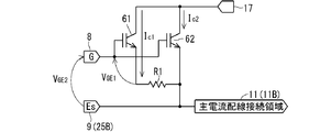
- FIG. It is a circuit diagram which shows the equivalent circuit of the semiconductor device of Embodiment 1.
- FIG. It is explanatory drawing which shows the structure of the semiconductor device which is Embodiment 2.
- FIG. It is explanatory drawing which shows the structure of the semiconductor device which is Embodiment 3.
- FIG. It is explanatory drawing which shows the structure of the semiconductor device which is Embodiment 4.
- It is a circuit diagram which shows the equivalent circuit of the semiconductor device shown in FIG. It is a circuit diagram which shows the equivalent circuit of the semiconductor device for comparison.
- FIG. 9 is an explanatory diagram showing the structure of a semiconductor device as a basic technology.
- the upper view of FIG. 9 is a cross-sectional view, and the lower view is a plan view.
- the GG cross section in the figure below is the figure above.
- the XYZ Cartesian coordinate system is shown in the upper and lower figures of FIG. 9, respectively.
- the insulating film 42 is shown as the uppermost layer.
- the semiconductor device 59 shown in FIG. 9 uses an IGBT as a switching element, and packages an IGBT chip 31, which is a semiconductor chip having an IGBT inside.
- the emitter electrode 33 is provided on the front surface of the IGBT chip 31, and the collector electrode 34 is provided on the back surface.
- the collector electrode 34 which is the back surface electrode, is electrically connected to the main current wiring 35 via the lower chip bottom bonding material 47.
- An insulating film 42 is provided on the surface of the emitter electrode 33, which is a surface electrode.
- the insulating film 42 has an opening region OP42 from the center to the + X direction.
- the opening region OP42 has a rectangular shape in which the length in the Y direction is longer than the length in the X direction in a plan view.
- the insulating film 42 further has an opening region OP43 on the outer peripheral portion on the ⁇ X direction side on the surface of the IGBT chip 31.
- the opening region OP43 has a rectangular shape in which the length in the Y direction is slightly longer than the length in the X direction in a plan view, and has a formation area smaller than that of the opening region OP42.
- the region in the opening region OP42 becomes the main current wiring connection region 41, and the region in the opening region OP43 becomes the emitter sense region.
- the bonding material 43 on the chip is provided on a part of the central region of the main current wiring connection region 41. That is, the emitter electrode 3 and the bonding material 43 on the chip are electrically connected by the contact between the lower surface S43 of the bonding material 43 on the chip and a part of the surface region of the main current wiring connection region 41.
- the forming area of the lower surface S43 of the bonding material 43 on the chip is smaller than the surface area of the main current wiring connection region 41.
- the main current wiring 36 is provided on the bonding material 43 on the chip, and the main current wiring 36 and the bonding material 43 on the chip are electrically connected.
- the emitter sense region of the emitter electrode 33 existing in the opening region OP43 is electrically connected to the control terminal 32 via the control wire 37.
- the gate pad 38 is electrically connected to a gate electrode which is an IGBT control electrode (not shown), and is provided on the surface of the IGBT chip 31 independently of the emitter electrode 33 without contacting the gate electrode 33. It is exposed.
- the gate pad 38 is electrically connected to a gate control terminal (not shown) via a gate control wire (not shown).
- control terminals of the IGBT there are a control terminal 32 for the emitter electrode 33 and a control terminal for the gate.
- Al or the like is used as a constituent material of the control wire 37 and the control wire for the gate, and an emitter sense pad (not shown) is placed on the emitter sense region in the opening region OP43 in order to establish an electrical connection between the control wire 37 and the collector electrode 34. It is common to provide. That is, by joining the control wire 37 to the surface of the emitter sense pad, it is possible to electrically connect the emitter sense region of the emitter electrode 33 and the control terminal 32 via the emitter sense pad and the control wire 37.
- the gate control wire is joined on the surface of the gate pad 38 like the control wire 37.
- the main current wiring 36 is electrically connected to the main current wiring 35 via the bonding material 43 on the chip, the emitter electrode 33, the IGBT in the IGBT chip 31, the collector electrode 34, and the bonding material 47 under the chip.
- the main current flows from the main current wiring 35 to the main current wiring 36 during the operation of the IGBT.
- the main current wirings 35 and 36 are external wiring for taking out the main current flowing through the IGBT.
- the current path IP9 shown in FIG. 9 shows the current flow in the main current.
- the gate pad 38 and the emitter sense pad are generally provided on the outer peripheral portion of the IGBT chip 31 in consideration of the connectivity with the module. That is, the emitter sense pad is provided on the outer peripheral region of the emitter electrode 33.
- FIG. 10 is a circuit diagram showing an equivalent circuit of the semiconductor device 59 shown in FIG.
- the resistance component of the emitter electrode 33 is taken into consideration.
- "39" means the above-mentioned emitter sense pad.
- the gate pad 38 is indicated by “G” and the emitter sense pad 39 is indicated by “Es”.
- the resistance component of the emitter electrode 33 is distributed in all the emitter electrodes 33 except the region bonded to the bonding material 43 on the chip, but for simplification, the emitter electrode is shown in FIG.
- the resistance component R9 as a lumped constant. That is, the IGBT in the IGBT chip 31 is classified into two, the IGBT in which the collector current Ic2 flows in the main current wiring connection region 41 and its vicinity is set as the IGBT 62, and the outer peripheral region of the emitter electrode 3 away from the main current wiring connection region 11 is used.
- the IGBT in which the collector current Ic1 is passed is defined as the IGBT 61.
- An emitter sense pad 39 is provided in the outer peripheral region of the emitter electrode 3.
- the collectors of the IGBTs 61 and 62 are commonly connected to the subchip joint material 47, and the gates of the IGBTs 61 and 62 are commonly connected to the gate pad 38.
- the emitter of the IGBT 62 is connected to the bonding material 43 on the chip, and the emitter of the IGBT 61 is connected to the emitter sense pad 39.
- An emitter electrode resistance component R9 exists between the emitters of the IGBTs 61 and 62.
- the emitter electrode resistance component R9 is a resistance component based on the distance from the lower surface of the bonding material 43 on the chip to the emitter sense pad 39 in the emitter electrode 33.
- the gate voltage VGE1 is applied between the gate pad 38 and the emitter sense pad 39 to put the IGBT in the IGBT chip 31 into an operating state.
- the collector current Ic1 flows through the IGBT 61, and the collector current Ic2 flows through the IGBT 62.
- the emitter electrode resistance component R9 exists between the emitters of the IGBTs 61 and 62, the emitter potential of the IGBT 62 becomes lower than the emitter potential of the IGBT 61 due to the voltage drop due to the emitter electrode resistance component R9.
- the gate voltage VGE2 of the IGBT 62 becomes higher than the gate voltage VGE1.
- VGE2 VGE1 + R9 ⁇ Ic1 ... (1)
- R9 is used as it is for the resistance value of the emitter electrode resistance component R9
- Ic2 is used as it is for the current value of the collector current Ic2.
- the collector current Ic2 in the semiconductor device 59 tends to increase with the in-plane potential distribution of the emitter electrode 33.
- this tendency becomes remarkable, so that the IGBT chip 31 may be thermally destroyed due to an increase in the collector current Ic2.
- the semiconductor device 59 which is a basic technology, has a problem of low reliability.
- the semiconductor device disclosed in Patent Document 1 focuses on the resistance component of the source electrode corresponding to the emitter electrode 33, changes the potential of the pad for source sense from the conventional structure, and is built in the switching element. We are trying to reduce the output variation of the current detection element. However, it was insufficient to improve the reliability of the semiconductor device disclosed in Patent Document 1.
- the embodiment described below is intended to solve the problems of the basic technology represented by the semiconductor device 59.
- FIG. 1 is a cross-sectional view
- the lower view is a plan view
- FIG. 2 is a plan view.
- the cross section AA in the lower part of FIG. 1 is the upper part of FIG. 1
- the cross section BB of FIG. 2 is also the upper part of FIG.
- the XYZ Cartesian coordinate system is shown in the upper and lower views of FIG. 1 and FIG. 2 respectively.
- FIG. 1 is a plan view with the uppermost portion as the insulating film 12, and FIG. 2 is a plan view with the uppermost portion as the emitter electrode 3.
- the semiconductor device 51 shown in FIGS. 1 and 2 uses an IGBT as a switching element, and packages an IGBT chip 1, which is a semiconductor chip having an IGBT inside.
- the emitter electrode 3 is provided on the surface of the IGBT chip 1.
- the emitter electrode 3 is formed in most of the region on the surface of the IGBT chip 1 except for the region where the gate pad 8, the emitter sense pad 9, and the emitter sense wiring 10 are formed.
- the collector electrode 4 is provided on the back surface of the IGBT chip 1.
- the collector electrode 4, which is the back surface electrode, is electrically connected to the main current wiring 5 via the bottom bonding member 17 provided below.
- the main current wiring 5 the lower part of the joint member 17 under the chip is the base.
- An insulating film 12 is provided on the surface of the emitter electrode 3.
- the insulating film 12 has an opening region OP12 from the center to the + X direction.
- the opening region OP12 has a rectangular shape in which the length in the Y direction is longer than the length in the X direction in a plan view.
- the insulating film 12 functions as a protective film, and is formed by, for example, applying polyimide on the surface of the emitter electrode 3.
- the region in the opening region OP12 is the main current wiring connection region 11.
- the bonding material 13 on the chip is provided on the entire area of the main current wiring connection area 11.
- the lower surface S13 of the bonding material 13 on the chip has a shape that matches the surface shape of the main current wiring connection region 11 in a plan view.
- the bonding material 13 on the chip corresponds to the “bonding material for chips”.
- the bottom surface S13 of the chip top bonding material 13 and the surface of the main current wiring connection region 11 come into contact with each other, so that the chip top bonding material 13 is electrically connected to the emitter electrode 3. Therefore, the bonding material 13 on the chip is provided on the entire surface of the main current wiring connection region 11.
- the main current wiring 6 is provided on the bonding material 13 on the chip, and the main current wiring 6 and the bonding material 13 on the chip are electrically connected.
- the gate pad 8 is provided on the surface of the IGBT chip 1 without contacting the emitter electrode 3, and the emitter sense pad 9 contacts the gate pad 8 and the emitter electrode 3 on the surface of the IGBT chip 1. It is provided without doing anything.
- the gate pad 8 and the emitter sense pad 9 are provided in the end region of the IGBT chip 1 on the ⁇ X direction side.
- the gate pad 8 and the emitter sense pad 9 each have a rectangular shape in which the length in the Y direction is slightly longer than the length in the X direction in a plan view.
- the gate pad 8 is electrically connected to the gate electrode of the IGBT via a gate wiring (not shown), and is electrically connected to an external control terminal for a gate (not shown) via a control wire for a gate (not shown). ..
- the gate electrode of the IGBT corresponds to the "control electrode of the switching element".
- the emitter sense wiring 10 is provided on the surface of the IGBT chip 1 and functions as a sense wiring that electrically connects the emitter electrode 3 and the emitter sense pad 9. Specifically, the emitter sense wiring 10 is provided extending from the emitter sense pad 9 in the + X direction, and as shown in FIG. 2, the emitter electrode is provided at the sense connection point 25 on the side surface of the main current wiring connection region 11. Contact with 3.
- the emitter electrode 3 is provided with a notch region extending in the X direction so as not to come into contact with the emitter sense wiring 10 other than the sense connection point 25.
- the emitter sense pad 9 is electrically connected to the control terminal 2 via the control wire 7. Specifically, by joining one end of the control wire 7 to the surface of the emitter sense pad 9, the emitter sense pad 9 and the control terminal 2 can be electrically connected.
- the gate control wire is joined on the surface of the gate pad 8 like the control wire 7.
- Al or the like is used as a constituent material for the control wire 7 and the gate control wire.
- control terminal of the IGBT which is the switching element in the IGBT chip 1
- control terminal 2 for the emitter electrode 3 there are a control terminal 2 for the emitter electrode 3 and a control terminal for the gate.
- the main current wiring 6 is electrically connected to the main current wiring 5 via the bonding material 13 on the chip, the emitter electrode 3, the IGBT in the IGBT chip 1, the collector electrode 4, and the bonding material 17 below the chip.
- the main current flows from the main current wiring 5 to the main current wiring 6 as a collector current.
- the main current wirings 5 and 6 are external wiring for taking out the main current flowing through the IGBT.
- the current path IP1 shown in FIGS. 1 and 2 shows the current flow in the main current.
- the emitter electrode 3, the emitter sense pad 9, and the emitter sense wiring 10 are integrally formed on the surface of the IGBT chip 1.
- the component of the IGBT is not formed in the invalid region 20 below the emitter sense pad 9 and the emitter sense wiring 10.
- the invalid region 20 is a region in which the switching element IGBT does not function.
- a field insulating film for element separation may be formed as the invalid region 20.
- the area below the gate pad 8 in the IGBT chip 1 is also an invalid area 20 in which the IGBT does not function.
- FIG. 3 is a circuit diagram showing an equivalent circuit of the semiconductor device 51 shown in FIGS. 1 and 2.
- the resistance component of the emitter electrode 3 is taken into consideration.
- the gate pad 8 is indicated by “G” and the emitter sense pad 9 is indicated by “Es”.
- the resistance component of the emitter electrode 3 is distributed in all the emitter electrodes 3 except the main current wiring connection region 11 bonded to the lower surface S13 of the bonding material 13 on the chip, but for simplification.
- the emitter electrode resistance component R1 is considered as a lumped constant. That is, the IGBT of the IGBT chip 1 is classified into two, the IGBT in which the collector current Ic2 flows in the main current wiring connection region 11 and its vicinity is set as the IGBT 62, and in the outer peripheral region of the emitter electrode 3 away from the main current wiring connection region 11.
- the IGBT through which the collector current Ic1 flows is defined as an IGBT 61. This outer peripheral region becomes the surface electrode remote region.
- the collectors of the IGBT 61 and 62 are commonly connected to the under-chip joint material 17, and the gate, which is the control electrode of the IGBT 61 and 62, is commonly connected to the gate pad 8 shown.
- the emitter of the IGBT 62 and the emitter sense pad 9 are electrically connected to the main current wiring connection region 11. At this time, the emitter electrode resistance component R1 exists between the emitter of the IGBT 61 and the emitter of the IGBT 61.
- This emitter electrode resistance component R1 is a resistance component based on the distance from the lower surface S13 of the bonding material 13 on the chip, that is, the main current wiring connection region 11 to the surface electrode remote region of the emitter electrode 3 in the emitter electrode 3. Therefore, the emitter of the IGBT 61 is connected to the main current wiring connection region 11 via the emitter electrode resistance component R1.
- the gate voltage VGE2 is applied between the gate pad 8 and the emitter sense pad 9, and the IGBT in the IGBT chip 1 is put into an operating state.
- the potential obtained from the emitter sense pad 9 becomes the control reference potential.
- the IGBT has a gate that is a control electrode, and the operation of the GIBT is controlled by applying a gate voltage VGE2, which is a control voltage with the potential of the emitter electrode 3 as a reference potential, to the gate of the IGBT.
- VGE2 is a control voltage with the potential of the emitter electrode 3 as a reference potential
- the collector current Ic1 flows through the IGBT 61, and the collector current Ic2 flows through the IGBT 62.
- the sum of the collector current Ic1 and the collector current Ic2 is the main current of the IGBT.
- the emitter potential of the IGBT 62 is not affected by the main current.
- the main current does not flow in the emitter sense wiring 10, and the charging / discharging current of the gate of the IGBT mainly flows. Since the charge / discharge current of the gate is a few orders of magnitude smaller than the main current, the voltage drop due to the current flowing through the emitter sense wiring 10 becomes a negligible level, and as a result, it is the potential of the emitter sense pad 9. The reference potential is not affected by the main current.
- the semiconductor device 51 Since the emitter electrode resistance component R1 exists between the emitters of the IGBTs 61 and 62, a voltage drop occurs between the emitters of the IGBTs 61 and 62 due to the emitter electrode resistance component R1.
- the semiconductor device 51 has a reference potential increase characteristic in which the emitter potential of the IGBT 61 becomes relatively higher than the emitter potential of the IGBT 62 due to the voltage drop. This reference potential rise characteristic corresponds to the "reference potential fluctuation characteristic".
- the remote region reference potential in the surface electrode remote region relatively far from the main current wiring connection region 11 is affected by the emitter electrode resistance component R1 based on the distance from the main current wiring connection region 11, and is higher than the control reference potential. It has a characteristic of increasing the reference potential.
- the gate voltage VGE1 of the IGBT 61 is lower than the gate voltage VGE2.
- VGE1 VGE2-R1 ⁇ Ic1 ... (2)
- R1 is used as it is for the resistance value of the emitter electrode resistance component R1
- Ic1 is used as it is for the current value of the collector current Ic1.
- the emitter potential of the IGBT 61 rises by (R1 ⁇ Ic1) due to the reference potential rising characteristic, so that the gate voltage VGE1 of the IGBT 61 is lower than the gate voltage VGE2. As a result, the collector current Ic1 flowing through the IGBT 61 can be reduced.
- the IGBT 61 has a reference potential rising characteristic based on the in-plane potential distribution of the emitter electrode 3. In particular, when a large current flows through the IGBT due to a short circuit or the like, this reference potential rise characteristic becomes remarkable.
- the collector current Ic1 flowing through the IGBT 61 decreases due to the reference potential rise characteristic, so that the increase in the main current of the IGBT can be effectively suppressed.
- the semiconductor device 51 effectively suppresses the increase in the main current by applying negative feedback to the gate voltage VGE1 of the IGBT 61 by the emitter electrode resistance component R1 when a large current is applied such as a short circuit.
- the reliability of the can be improved.
- the semiconductor device 51 suppresses the total amount of the collector current (Ic1 + Ic2) by controlling the current so that the collector current Ic1 decreases even if a large current such as a short circuit flows and the collector current Ic2 increases. Thereby, the reliability of the device can be improved.
- the value of the emitter electrode resistance component R1 can be arbitrarily adjusted. For example, if the surface area of the main current wiring connection region 11 is reduced by reducing the size of the opening region OP12, the emitter electrode resistance component R1 becomes large and the reference potential increase characteristic can be enhanced.
- the emitter electrode resistance component R1 is minute, power loss occurs. Therefore, when applying it to an actual semiconductor device, consider the trade-off between the degree of current decrease tendency of the collector current Ic1 and the increase in power loss. Therefore, it is necessary to properly design the dimensions of the opening region OP12.
- the chip is out of the surface region of the main current wiring connection region 11. Since the size of the emitter electrode resistance component R1 changes depending on the area in contact with the upper bonding material 13, optimum design becomes difficult.
- the surface shape of the lower surface S13 of the bonding material 13 on the chip is matched with the surface shape of the main current wiring connection region 11, and the entire surface region of the main current wiring connection region 11 and the chip are formed.
- the lower surface S13 of the upper bonding material 13 is bonded.
- the entire region of the surface of the main current wiring connection region 11 existing in the opening region OP12 of the insulating film 12 and the lower surface S13 of the bonding material 13 on the chip are brought into contact with each other to bring the emitter electrodes 3 and the chip into contact with each other.
- a full-face bonding structure for electrical connection between the upper bonding materials 13 is realized.
- the emitter electrode resistance component R1 can be accurately set according to the dimensions of the opening region OP12.
- the lower surface S13 of the lower surface S13 has a surface shape that matches the surface of the main current wiring connection region 11.
- the bonding material 13 on the chip when solder is used as the bonding material 13 on the chip, the inside of the opening region OP12 of the insulating film 12 is plated and the bonding material 13 on the chip is embedded in the opening region OP12 without a gap, so that the main current wiring connection region 11 It is possible to obtain a chip-on-chip bonding material 13 having a lower surface S13 in contact with the entire surface.
- the semiconductor device 51 of the first embodiment has the following features (1) to (3).
- the lower surface S13 of the bonding material 13 on the chip has a shape that matches the surface shape of the main current wiring connection region 11 in a plan view.
- the emitter sense wiring 10 is directly connected to the side surface of the main current wiring connection region 11.
- the IGBT chip 1 has an invalid region 20 in which the IGBT does not function in the region below the emitter sense pad 9 and the emitter sense wiring 10.
- the bonding material 13 on the chip corresponds to the "bonding material for the chip”
- the main current wiring connection area 11 corresponds to the "wiring connection area”
- the emitter sense wiring. 10 corresponds to "sense wiring”
- IGBT chip 1 corresponds to “semiconductor chip”
- emitter sense pad 9 corresponds to "sense pad”
- IGBT corresponds to "switching element”.
- the control reference potential obtained from the emitter sense pad 9 during the operation of the IGBT is the main current wiring connection region 11. It is not affected by the emitter electrode resistance component R1 based on the distance from.
- the gate voltage VGE2 becomes equal to the control voltage value VG0.
- the emitter potential of the IGBT 61 is affected by the emitter electrode resistance component R1 based on the distance from the main current wiring connection region 11, and has a reference potential increase characteristic that is higher than the emitter potential of the IGBT 62. Have.
- the gate voltage VGE1 of the IGBT 61 is lower than the gate voltage VGE2 as shown in the above equation (2).
- the emitter potential of the IGBT 61 corresponds to the "remote region reference potential" in the surface electrode remote region relatively far from the main current wiring connection region 11, and the emitter potential of the IGBT 62 is for control obtained from the emitter sense pad 9.
- the "reference potential rise characteristic" corresponds to the "reference potential fluctuation characteristic”.
- the semiconductor device 51 of the first embodiment when a large current flows as the main current flowing through the emitter electrode 3 at the time of a short circuit or the like, the amount of current of the collector current Ic1 flowing through the remote region of the surface electrode is accompanied by the reference potential rising characteristic. Can be reduced.
- the semiconductor device 51 of the first embodiment can effectively suppress an increase in the current amount of the main current of the IGBT by reducing the collector current Ic1 and improve the reliability of the device.
- the emitter electrode 3 corresponds to the “surface electrode”. Further, when the IGBTs in the IGBT chip 1 are classified into IGBTs 61 and 62, the gate voltage VGE2 corresponds to the "control voltage” for the IGBT 62, and the gate voltage VGE1 corresponds to the "control voltage” for the IGBT 61.
- FIG. 4 is an explanatory diagram showing the structure of the semiconductor device 52 according to the second embodiment of the present disclosure.
- the upper view of FIG. 4 is a cross-sectional view, and the lower view is a plan view.
- the CC cross section of the lower figure of FIG. 4 is the upper view of FIG. 4, and the XYZ Cartesian coordinate system is shown in each of the upper and lower views of FIG.
- the semiconductor device 52 shown in FIG. 4 uses an IGBT as a switching element, and packages an IGBT chip 1B, which is a semiconductor chip having an IGBT inside.
- the emitter electrode 3 is provided on the front surface of the IGBT chip 1B, and the collector electrode 4 is provided on the back surface.
- the collector electrode 4 serving as the back surface electrode is electrically connected to the main current wiring 5 via the chip bottom bonding material 17.
- each of the plurality of main current wires 14 is electrically connected to the emitter electrode 3 by contacting with the corresponding chip connection point 23B among the plurality of chip connection points 23B on the surface of the emitter electrode 3. ..
- the plurality of chip connection points 23B are discretely provided near the center in the X direction along the Y direction. In this way, one end of each of the plurality of main current wires 14 is joined on the surface of the emitter electrode 3. The other ends of the plurality of main current wires 14 are joined to the main current wiring 6 on the surface.
- the plurality of main current wires 14 correspond to "a plurality of chip wires".
- control wire 7B is electrically connected to the emitter electrode 3 by contacting with the sense connection point 25B on the surface of the emitter electrode 3. That is, one end of the control wire 7B is joined on the surface of the emitter electrode 3.
- the sense connection point 25B is provided near the third and fourth chip connection points 23B from the + Y direction side among the plurality of chip connection points 23B.
- the control wire 7B and the plurality of main current wires 14 are electrically and independently provided without contacting each other.
- the other end of the control wire 7B is joined to the control terminal 2.
- the region including the plurality of chip connection points 23B in the emitter electrode 3 is defined as the main current wiring connection region 11B, and the position farthest from the main current wiring connection region 11B in the emitter electrode 3 is defined as the electrode remote position.
- the outer peripheral surface on the ⁇ X side is the electrode remote position.
- the emitter electrode 3 corresponds to a "surface electrode”
- the main current wiring connection region 11B corresponds to a "wiring connection region”.
- the sense connection point 25B satisfies the connection point arrangement condition provided at a position closer to the chip connection point 23B among the chip connection point 23B and the electrode remote position.
- the sense connection point 25B may satisfy the above connection point arrangement condition in relation to at least one main current wire 14 among the plurality of main current wires 14. Further, the potential obtained from the sense connection point 25B becomes the control reference potential.
- the gate pad 8 is provided on the surface of the IGBT chip 1B without contacting the emitter electrode 3.
- the gate pad 8 is provided in the end region of the IGBT chip 1B on the ⁇ X direction side.
- the gate pad 8 has a rectangular shape in which the length in the Y direction is slightly longer than the length in the X direction in a plan view. Further, the region below the gate pad 8 in the IGBT chip 1B is an invalid region in which the IGBT does not function.
- the gate pad 8 is electrically connected to the gate electrode of the IGBT via a gate wiring (not shown), and is electrically connected to a gate control terminal (not shown) via a control wire for a gate (not shown).
- the gate control wire is joined on the surface of the gate pad 8. Al or the like is used as a constituent material of the control wire 7B, the main current wire 14, and the gate control wire.
- the second embodiment has the control terminal 2 for the emitter electrode 3 and the control terminal for the gate as the control terminal of the IGBT which is the switching element in the IGBT chip 1B as in the first embodiment. There is.
- the main current wiring 6 is electrically connected to the main current wiring 5 via a plurality of main current wires 14, an emitter electrode 3, an IGBT in the IGBT chip 1B, a collector electrode 4, and a subchip bonding material 17.
- the main current flows from the main current wiring 5 to the main current wiring 6 as a collector current.
- the main current wirings 5 and 6 are external wiring for taking out the main current flowing through the IGBT.
- the current path IP2 shown in FIG. 4 shows the current flow in the main current.
- the semiconductor device 52 of the second embodiment appears in the equivalent circuit shown in FIG. 3, as in the first embodiment. However, the main current wiring connection area 11 shown in FIG. 3 is replaced with the main current wiring connection area 11B, and the emitter sense pad 9 is replaced with the sense connection point 25B.
- the IGBT in which the collector current Ic2 flows in the main current wiring connection region 11B and its vicinity is set as the IGBT 62, and the collector current Ic1 is set in the outer peripheral region of the emitter electrode 3 away from the main current wiring connection region 11B.
- the IGBT to be flowed is set to the IGBT 61. This outer peripheral region becomes the surface electrode remote region.
- the sense connection point 25B close to one of the plurality of chip connection points 23B. That is, it is desirable to arrange the sense connection point 25B close to any of the plurality of chip connection points 23B so that the resistance component between the sense connection point 25B and the main current wiring connection area 11B can be ignored.
- the semiconductor device 52 of the second embodiment negatively feeds the gate voltage VGE1 of the IGBT 61 due to the reference potential rising characteristic of the IGBT 61 when a large current is applied such as a short circuit, so that the main current can be increased.
- the increase can be effectively suppressed and the reliability of the device can be improved.
- the semiconductor device 52 of the second embodiment has the following feature (4).
- the sense connection point 25B of the control wire 7B satisfies the connection point arrangement condition provided at a position closer to the chip connection point 23B among the chip connection point 23B and the electrode remote position in the emitter electrode 3.
- control wire 7B corresponds to the “sense connection member” or the “sense wire”
- the emitter electrode 3 corresponds to the “surface electrode”.
- the semiconductor device 52 of the second embodiment has the above-mentioned feature (4). Therefore, in the semiconductor device 52, by arranging the sense connection point 25B close to one of the plurality of chip connection points 23B, the control point 25B can be obtained from the sense connection point 25B during operation of the IGBT.
- the reference potential is almost unaffected by the emitter electrode resistance component R1 based on the distance from the main current wiring connection region 11B.
- the gate voltage VGE2 becomes equal to the control voltage value VG0.
- the emitter potential of the IGBT 61 is affected by the emitter electrode resistance component R1 based on the distance from the main current wiring connection region 11B, and has a reference potential increase characteristic that is higher than the emitter potential of the IGBT 62. Have.
- the gate voltage VGE1 of the IGBT 61 is lower than the gate voltage VGE2 as shown in the above equation (2).
- the emitter potential of the IGBT 61 corresponds to the "remote region reference potential" in the surface electrode remote region relatively far from the wire connection region.
- the collector current Ic1 flowing through the remote region of the surface electrode is accompanied by the reference potential rising characteristic of the IGBT 61. The amount of current can be reduced.
- the semiconductor device 52 of the second embodiment can effectively suppress an increase in the current amount of the main current of the IGBT by reducing the collector current Ic1 and improve the reliability of the device.
- the semiconductor device 52 of the second embodiment can relatively easily electrically connect the sense connection point 25B of the emitter electrode 3 and the control terminal 2 by the control wire 7B.
- the semiconductor device 52 of the second embodiment can take out a relatively large main current to the outside by making an electrical connection with the emitter electrode 3 by means of a plurality of main current wires 14.
- the emitter electrode 3 corresponds to the “surface electrode”. Further, when the IGBTs in the IGBT chip 1 are classified into IGBTs 61 and 62, the gate voltage VGE2 corresponds to the "control voltage” for the IGBT 62, and the gate voltage VGE1 corresponds to the "control voltage” for the IGBT 61. Further, the control wire 7B corresponds to the "sense joining member” or the “sense wire”, and the main current wire 14 corresponds to the "chip wire”.
- the sense connection point 25B of the control wire 7B can exhibit the above effect by satisfying the above-mentioned connection point arrangement condition.
- the sense connection point 25B be as close as possible to any one of the plurality of chip connection points 23B. This is because the emitter electrode resistance component R1 of the emitter electrode 3 can be increased to enhance the effect of suppressing the amount of main current.
- the sense connection point 25B be closer to the connection point existing in the center of the emitter electrode 3 among the plurality of chip connection points 23B.
- FIG. 5 is an explanatory diagram showing the structure of the semiconductor device 53 according to the third embodiment of the present disclosure.
- the upper view of FIG. 5 is a cross-sectional view, and the lower view is a plan view.
- the DD cross section of the lower figure of FIG. 5 is the upper view of FIG. 5, and the XYZ Cartesian coordinate system is shown in each of the upper and lower views of FIG.
- the semiconductor device 53 shown in FIG. 5 uses an IGBT as a switching element, and packages an IGBT chip 1C, which is a semiconductor chip having an IGBT inside.
- IGBT chip 1C which is a semiconductor chip having an IGBT inside.
- the gate pad 8 is provided on the surface of the IGBT chip 1C without contacting the emitter electrode 3, and the emitter sense pad 9 contacts the gate pad 8 and the emitter electrode 3 on the surface of the IGBT chip 1C. It is provided without doing anything.
- the gate pad 8 and the emitter sense pad 9 are provided in the end region of the IGBT chip 1C on the ⁇ X direction side.
- the gate pad 8 and the emitter sense pad 9 each have a rectangular shape in which the length in the Y direction is slightly longer than the length in the X direction in a plan view.
- the gate pad 8 is electrically connected to the gate electrode of the IGBT via a gate wiring (not shown), and is electrically connected to a gate control terminal (not shown) via a control wire for a gate (not shown).
- the emitter sense wiring 10 is provided on the surface of the IGBT chip 1C and is a sense wiring that electrically connects the emitter electrode 3 and the emitter sense pad 9. Specifically, the emitter sense wiring 10 extends from the emitter sense pad 9 in the + X direction and comes into direct contact with the emitter electrode 3 at the sense connection point 25C on the side surface of the main current wiring connection region 11.
- the emitter electrode 3 is provided with a notched region extending in the X direction so as not to come into contact with the emitter sense wiring 10 other than the sense connection point 25C.
- the sense connection point 25C satisfies the connection point arrangement condition provided at a position closer to the chip connection point 23B among the chip connection point 23B and the electrode remote position in the emitter electrode 3.
- the sense connection point 25C may satisfy the above connection point arrangement condition in relation to at least one main current wire 14 among the plurality of main current wires 14.
- the sense connection point 25C is provided near the fifth chip connection point 23B from the + Y direction side among the plurality of chip connection points 23B, and the above connection point arrangement condition is satisfied. I am satisfied.
- the emitter sense pad 9 is electrically connected to the control terminal 2 via the control wire 7. Specifically, by joining the tip of the control wire 7 to the surface of the emitter sense pad 9, the emitter sense pad 9 and the control terminal 2 can be electrically connected.
- Al or the like is used as a constituent material of the control wire 7, the main current wire 14, and the gate control wire.
- the component of the IGBT is not formed in the invalid region 20C below the emitter sense pad 9 and the emitter sense wiring 10.
- the invalid region 20C is a region in which the switching element IGBT does not function.
- the region below the gate pad 8 is also an invalid region 20C in which the IGBT does not function.
- control terminal 2 for the emitter electrode 3 and the control for the gate are used as the control terminals of the IGBT which is the switching element in the IGBT chip 1C. It has a terminal.
- the main current wiring 6 is electrically connected to the main current wiring 5 via a plurality of main current wires 14, an emitter electrode 3, an IGBT in the IGBT chip 1C, a collector electrode 4, and a subchip bonding material 17.
- the main current flows from the main current wiring 5 to the main current wiring 6 as a collector current.
- the main current wirings 5 and 6 are external wiring for taking out the main current flowing through the IGBT.
- the current path IP3 shown in FIG. 5 shows the current flow in the main current.
- the semiconductor device 53 of the third embodiment appears in the equivalent circuit shown in FIG. 3, as in the first and second embodiments. However, the main current wiring connection area 11 shown in FIG. 3 is replaced with the main current wiring connection area 11B.
- the semiconductor device 53 of the third embodiment can improve the reliability of the device as in the semiconductor device 51 and the second embodiment.
- the semiconductor device 53 of the third embodiment further exerts the following effects.
- the gate pad 8 and the emitter sense pad 9 are used instead of the control wire 7B as the sense connecting member. Therefore, in the semiconductor device 53, the interference does not occur even if the sense connection point 25C is brought close to the chip connection point 23B. Therefore, the distance between the chip connection point 23B and the sense connection point 25C is shortened to reduce the distance between the chip connection point 23B and the sense connection point 25C.
- the resistance component R1 can be increased to enhance the effect of suppressing the amount of the main current.
- the semiconductor device 53 of the third embodiment is electrically connected to the emitter electrode 3 with good stability by connecting the emitter sense wiring 10 at the sense connection point 25C relatively close to the chip connection point 23B. You can make a connection.
- the emitter potential of the IGBT 62 is the main current in the equivalent circuit shown in FIG. Not affected.
- the emitter sense wiring 10 corresponds to the “sense wiring”
- the emitter electrode 3 corresponds to the “surface electrode”
- the IGBT chip 1C corresponds to the “semiconductor chip”
- the emitter corresponds to the emitter.
- the sense pad 9 corresponds to the "sense pad”
- the emitter sense wiring 10 corresponds to the "sense wiring”
- the IGBT corresponds to the "switching element”.
- the emitter potential of the IGBT 62 is a control reference potential obtained from the emitter sense pad 9.
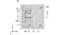
- FIG. 6 and 7 are explanatory views showing the structure of the semiconductor device 54 according to the fourth embodiment of the present disclosure.
- the upper view of FIG. 6 is a cross-sectional view
- the lower view is a plan view
- FIG. 7 is a plan view.
- the EE cross section of the lower figure of FIG. 6 is the upper view of FIG. 6, and the FF cross section of FIG. 7 is also the upper view of FIG.
- the XYZ Cartesian coordinate system is shown in the upper and lower views of FIG. 6 and FIG. 7 respectively.
- FIG. 6 is a plan view in which the uppermost portion is an insulating film 12
- FIG. 7 is a plan view in which the uppermost portion is an emitter electrode 3.
- the semiconductor device 54 shown in FIGS. 6 and 7 uses an IGBT as a switching element, and packages an IGBT chip 1D, which is a semiconductor chip having an IGBT inside.
- the current path IP4 shown in FIGS. 6 and 7 shows the current flow in the main current.
- the semiconductor device 54 of the fourth embodiment has the following features (5) to (7) in addition to the features (1) to (3) of the semiconductor device 51.
- the IGBT chip 1D further has a current detection IGBT that performs a switching operation equivalent to that of the original IGBT, and the current detection IGBT is provided in the current detection element forming region 27 of the IGBT chip 1D.
- a current detection output pad 15 provided on the surface of the current detection element forming region 27 of the IGBT chip 1D without contacting the emitter electrode 3 and through which a detection current flows during operation of the current detection IGBT is further provided. .. (7)
- the current obtained from the current detection output pad 15 is the sense current Is.
- the IGBT chip 1D corresponds to the "semiconductor chip”
- the IGBT corresponds to the "switching element”
- the current detection IGBT corresponds to the "current detection element”.
- the emitter electrode 3 corresponds to the "surface electrode”
- the current detection output pad 15 corresponds to the "current detection pad”.
- the component of the IGBT is not formed in the invalid region 20D below the emitter sense pad 9 and the emitter sense wiring 10.
- This invalid region 20D is a region in which the switching element IGBT does not function.
- the region below the gate pad 8 is also an invalid region 20D in which the IGBT does not function.
- an invalid region 20D is also formed around the current detection element forming region 27 in the IGBT chip 1D. Since the invalid region 20D functions as an element separation region, the current detection IGBT in the current detection element forming region 27 is provided independently of the original IGBT below the emitter electrode 3.
- the current detection output pad 15 is provided on the current detection element forming region 27 without contacting the emitter electrode 3, the gate pad 8, and the emitter sense pad 9, and functions as an emitter electrode of the current detection IGBT. As shown in the figure, it is electrically connected to the control terminal 2D via the control wire 7D. In this way, the current detection output pad 15 is provided independently of the emitter electrode 3.
- FIG. 8 is a circuit diagram showing an equivalent circuit of the semiconductor device 54 shown in FIGS. 6 and 7.
- the resistance component of the emitter electrode 3 is taken into consideration.
- the gate pad 8 is indicated by “G”
- the emitter sense pad 9 is indicated by “Es”
- the current detection output pad 15 is indicated by “S”.
- the emitter electrode resistance component R1 is considered as a lumped constant. That is, the IGBT of the IGBT chip 1D is classified into two, the IGBT in which the collector current Ic2 flows in the main current wiring connection region 11 and its vicinity is set as the IGBT 62, and the IGBT is located in the outer peripheral region of the emitter electrode 3 away from the main current wiring connection region 11.
- the IGBT through which the collector current Ic1 flows is defined as an IGBT 61. This outer peripheral region becomes the surface electrode remote region.
- FIG. 11 is a circuit diagram showing an equivalent circuit of the semiconductor device 59B for comparison, which has the same current detection function as the semiconductor device 54.
- the semiconductor device 59B has a configuration in which a current detection output pad 15 is added to the semiconductor device 59 of the basic technology shown in FIGS. 9 and 10. Further, in FIG. 11, the gate pad 38 is indicated by “G”, the emitter sense pad 39 is indicated by “Es”, and the current detection output pad 15 is indicated by “S”.
- the emitter electrode resistance component R9 is considered as a lumped constant. That is, the IGBT of the IGBT chip 31 is classified into two, the IGBT in which the collector current Ic2 is passed in the main current wiring connection region 41 and its vicinity is referred to as the IGBT 62, and the IGBT in which the collector current Ic1 is passed in the emitter sense pad 39 and its vicinity is referred to as the IGBT 61. It is supposed to be.
- the current detection IGBT is set to the IGBT 63, the gate of the IGBT 63 is connected to the gate pad 8, and the emitter is connected to the current detection output pad 15 without passing through the emitter electrode resistance component R1 or R9. Will be done.
- the current flowing through the IGBT 63 is defined as the sense current Is.
- the current detection output pad 15 and the emitter sense pad 9 or the emitter sense pad 39 are short-circuited.
- the semiconductor device 59B is affected by the emitter electrode resistance component R9, and the collector current Ic2 of the IGBT 62 tends to increase.
- both the gate voltage VGE1 of the IGBT 61 and the gate voltage VGE3 of the IGBT 63 are not affected by the emitter electrode resistance component R9.
- both the gate voltage VGE1 and the gate voltage VGE3 are equal to the control voltage value VG0.
- the collector current Ic1 and the sense current Is are not affected by the increase in the collector current Ic2.
- the semiconductor device 59B has a detection characteristic that the collector current Ic1 can be accurately detected by the sense current Is, but the collector current Ic2 cannot be accurately detected by the sense current Is.
- the semiconductor device 54 of the fourth embodiment has a tendency that the collector current Ic1 of the IGBT 61 decreases due to the influence of the emitter electrode resistance component R1 as in the semiconductor device 51.
- the gate voltage VGE2 of the IGBT 62 is not affected by the emitter electrode resistance component R1.
- the gate voltage VGE3 of the IGBT 63 is not affected by the emitter electrode resistance component R1. This is because the current detection element forming region 27 is below the current detection output pad 15, and the current detection output pad 15 can be formed relatively small. Therefore, the gate voltage VGE3 during operation of the current detection IGBT is current detection. This is because it is hardly affected by the resistance component of the output pad 15.
- both the gate voltage VGE2 and the gate voltage VGE3 are equal to the control voltage value VG0.
- the collector current Ic2 and the sense current Is are not affected by the decrease of the collector current Ic1.
- the semiconductor device 54 has a detection characteristic that the collector current Ic2 can be accurately detected by the sense current Is, but the collector current Ic1 cannot be accurately detected by the sense current Is.
- the gate voltage VGE1 becomes lower than the gate voltage VGE2, and the amount of the collector current Ic1 flowing in the remote region of the surface electrode decreases.
- the current detection IGBT It is possible to improve the detection sensitivity of the main current based on the sense current Is flowing through the.
- the IGBT corresponds to the "switching element” and the emitter electrode 3 corresponds to the "surface electrode”.
- the gate voltage VGE1 corresponds to the "control voltage” for the IGBT 61
- the gate voltage VGE2 corresponds to the "control voltage” for the IGBT 62.
- the current detection output pad 15 corresponds to the "current detection pad”
- the gate voltage VGE3 corresponds to the "control voltage” for the IGBT 63.
- a structure is shown in which a current detection output pad 15, a current detection element forming region 27, and the like are added based on the 51st embodiment.
- the structure is not limited to this, and a structure in which the current detection output pad 15 and the current detection element forming region 27 are added based on the semiconductor device 52 or the semiconductor device 53 may be adopted as a modification.
- the inherent effect of the fourth embodiment can be similarly exerted.
- the IGBT is used as the switching element.
- the semiconductor device 51 of the first embodiment will be described as a representative.
- the IGBT provided in the IGBT chip 1 of the semiconductor device 51 has a PN junction, and a loss of the rising voltage (1VF ⁇ 0.7V) always occurs when energized.
- VF means a forward voltage of the diode, and a loss of 1 VF is generated between the emitter electrode 3 and the collector electrode 4.
- the semiconductor device 51 even if a loss due to a minute emitter electrode resistance component R1 of the emitter electrode 3 which is a surface electrode occurs, the loss of 1 VF described above due to the original rising voltage becomes dominant. Therefore, in the semiconductor device 51, even if the emitter electrode resistance component R1 is designed to be large, it is easy to tolerate an increase in loss, and the reliability of the device can be further improved.
- the IGBT when the IGBT is used as the switching element provided in the IGBT chip 1, the IGBT has a characteristic that the rising voltage at the time of energization is not easily affected by the loss due to the emitter electrode resistance component R1 of the emitter electrode 3, and thus is reliable. A semiconductor device 51 having high performance can be obtained.
- MOSFET complementary metal-oxide-semiconductor
- Si silicon
- SiC silicon carbide
- the switching element represented by the IGBT is generally formed of silicon (Si), but as a modification, the switching element is configured by a wide bandgap semiconductor having a larger bandgap than silicon. Is possible. Wide bandgap semiconductors include, for example, silicon carbide, gallium nitride based materials or diamond.
- the IGBT is configured by the wide bandgap semiconductor. Since this IGBT has high withstand voltage resistance and high allowable current density, it is possible to reduce the size of the IGBT. Therefore, the modification of the semiconductor device 51 has an effect that the device as a semiconductor module can be miniaturized by providing the miniaturized IGBT in the IGBT chip 1.
- the wide-gap semiconductor has high heat resistance, it is possible to reduce the size of the heat radiation fins of the heat sink and to cool the water-cooled portion by air. Therefore, the modification of the semiconductor device 51 is further reduced in size as a semiconductor module. Can be planned.
- the IGBT in the modified example of the semiconductor device 51 is composed of a wide-gap semiconductor.
- the wide bandgap semiconductor has high withstand voltage resistance, high allowable power density, and high heat resistance, the modified example of the semiconductor device 51 can be miniaturized.
- the wide-gap semiconductor has a low power loss, it is possible to improve the efficiency of the IGBT element, and by extension, the efficiency of the semiconductor module having the IGBT can be improved. Due to the above-mentioned characteristics of high heat resistance and low loss, it is easy to tolerate an increase in loss deterioration due to the emitter electrode resistance component R1 of the emitter electrode 3.
- the modified example of the semiconductor device 51 can exert the various effects described above.
- the IGBT in the above-mentioned effect corresponds to the "switching element”
- the IGBT chip 1 corresponds to the “semiconductor chip”
- the emitter electrode 3 corresponds to the "surface electrode”.
- the switching element represented by the IGBT provided in the IGBT chips 1, 1B to 1D can be applied regardless of whether it is a planar type or a trench type.
- each embodiment can be freely combined, and each embodiment can be appropriately modified or omitted.
- 1,1B to 1D IGBT chip 2 control terminal, 3 emitter electrode, 4 collector electrode, 5,6 main current wiring, 7,7B control wire, 8 gate pad, 9 emitter sense pad, 10 emitter sense wiring, 11 main current Wiring connection area, 12 insulating film, 13 chip bonding material, 14 main current wire, 15 current detection output pad, 20, 20C, 20D invalid area, 27 current detection element formation area.
Landscapes
- Semiconductor Integrated Circuits (AREA)
- Metal-Oxide And Bipolar Metal-Oxide Semiconductor Integrated Circuits (AREA)
Abstract
Description
(1) チップ用接合材の下面は平面視して配線接続領域の表面形状と合致する形状を有する。
(2) センス配線は配線接続領域に接続される。
(3) 半導体チップは、センスパッド及びセンス配線の下方の領域において、スイッチング素子が機能しない無効領域を有する。
(4) センス用接続点は、チップ用接続点及び上記電極遠隔位置のうち、チップ用接続点に近い位置に設けられる接続点配置条件を満足する。
図9は基礎技術となる半導体装置の構造を示す説明図である。図9の上図が断面図であり、下図が平面図である。下図のG-G断面が上図となる。図9の上図及び下図にそれぞれXYZ直交座標系を記す。図9の下図では最上層として絶縁膜42を示している。
式(1)において、エミッタ電極抵抗成分R9の抵抗値に「R9」をそのまま用い、コレクタ電流Ic2の電流値に「Ic2」をそのまま用いている。
図1及び図2は本開示の実施の形態1である半導体装置51の構造を示す説明図である。図1の上図が断面図であり、下図が平面図であり、図2が平面図である。図1の下図のA-A断面が図1の上図となり、図2のB-B断面も図1の上図となる。図1の上図及び下図並びに図2それぞれにXYZ直交座標系を記す。
式(2)において、エミッタ電極抵抗成分R1の抵抗値に「R1」をそのまま用い、コレクタ電流Ic1の電流値に「Ic1」をそのまま用いている。
(1) チップ上接合材13の下面S13は主電流配線接続領域11の表面形状と平面視して合致する形状を有する。
(2) エミッタセンス配線10は、主電流配線接続領域11の側面に直接接続される。
(3) IGBTチップ1は、エミッタセンスパッド9及びエミッタセンス配線10の下方の領域において、IGBTが機能しない無効領域20を有する。
図4は本開示の実施の形態2である半導体装置52の構造を示す説明図である。図4の上図が断面図であり、下図が平面図である。図4の下図のC-C断面が図4の上図となり、図4の上図及び下図それぞれにXYZ直交座標系を記す。
(4) 制御ワイヤ7Bのセンス用接続点25Bは、エミッタ電極3におけるチップ用接続点23B及び電極遠隔位置のうち、チップ用接続点23Bに近い位置に設けられる接続点配置条件を満足する。
図5は本開示の実施の形態3である半導体装置53の構造を示す説明図である。図5の上図が断面図であり、下図が平面図である。図5の下図のD-D断面が図5の上図となり、図5の上図及び下図それぞれにXYZ直交座標系を記す。
図6及び図7は本開示の実施の形態4である半導体装置54の構造を示す説明図である。図6の上図が断面図であり、下図が平面図であり、図7が平面図である。図6の下図のE-E断面が図6の上図となり、図7のF-F断面も図6の上図となる。図6の上図及び下図並びに図7それぞれにXYZ直交座標系を記す。
(5) IGBTチップ1Dは、本来のIGBTと等価なスイッチング動作を行う電流検出用IGBTをさらに有し、電流検出用IGBTはIGBTチップ1Dの電流検出素子形成領域27内に設けられる。
(6) IGBTチップ1Dの電流検出素子形成領域27の表面上に、エミッタ電極3に接触することなく設けられ、電流検出用IGBTの動作時に検出電流が流れる電流検出出力パッド15をさらに備えている。
(7) 電流検出出力パッド15より得られる電流がセンス電流Isとなる。
実施の形態1~実施の形態4の半導体装置51~54では、スイッチング素子としてIGBTを用いている。スイッチング素子としてIGBTを用いることにより、以下の効果を奏する。以下、実施の形態1の半導体装置51を代表して説明する。
Claims (8)
- 内部にスイッチング素子を有する半導体チップと、
前記半導体チップの表面上に設けられ、前記スイッチング素子の動作時に主電流が流れる表面電極とを備え、前記スイッチング素子は制御電極を有し、前記表面電極の電位を基準電位とした制御電圧を前記制御電極に印加することにより前記スイッチング素子は動作制御され、
前記表面電極上に設けられる絶縁膜をさらに備え、前記絶縁膜は開口領域を有し、前記表面電極において前記開口領域内の領域が配線接続領域となり、
下面を有し、下面と前記配線接続領域の表面とが接触することにより、前記表面電極に電気的に接続されるチップ用接合材と、
前記半導体チップの表面上に前記表面電極と独立して設けられるセンスパッドと、
前記半導体チップの表面上に設けられ、前記表面電極と前記センスパッドとを電気的に接続するセンス配線とをさらに備え、
前記センスパッドの電位が前記スイッチング素子の制御用基準電位となり、
前記チップ用接合材の下面は平面視して前記配線接続領域の表面形状と合致する形状を有し、
前記センス配線は前記配線接続領域に接続され、
前記半導体チップは、前記センスパッド及び前記センス配線の下方の領域において、前記スイッチング素子が機能しない無効領域を有する、
半導体装置。 - 内部にスイッチング素子を有する半導体チップと、
前記半導体チップの表面上に設けられ、前記スイッチング素子の動作時に主電流が流れる表面電極とを備え、前記スイッチング素子は制御電極を有し、前記表面電極の電位を基準電位とした制御電圧を前記制御電極に印加することにより、前記スイッチング素子は動作制御され、
前記表面電極の表面上のチップ用接続点で接触することにより、前記表面電極と電気的に接続されるチップ用ワイヤと、
前記表面電極のセンス用接続点で接触することにより、前記表面電極と電気的に接続されるセンス用接続部材と、
前記センス用接続点の電位が前記スイッチング素子の制御用基準電位となり、前記表面電極において前記チップ用接続点を含む領域が配線接続領域として規定され、前記表面電極において前記配線接続領域から最も離れた位置が電極遠隔位置として規定され、
前記センス用接続点は、前記チップ用接続点及び前記電極遠隔位置のうち、前記チップ用接続点に近い位置に設けられる接続点配置条件を満足する、
半導体装置。 - 請求項2記載の半導体装置であって、
前記センス用接続部材はセンス用ワイヤを含み、
前記センス用接続点は、前記表面電極の表面に存在する、
半導体装置。 - 請求項2記載の半導体装置であって、
前記センス用接続部材は
前記半導体チップの表面上に前記表面電極と独立して設けられるセンスパッドと、
前記半導体チップの表面上に設けられ、前記表面電極と前記センスパッドとを電気的に接続するセンス配線とを含み、
前記センス用接続点は、前記配線接続領域の側面に存在し、
前記センス配線は前記センス用接続点で前記表面電極と接触することにより、前記表面電極と電気的に接続され、
前記半導体チップは、前記センスパッド及び前記センス配線の下方の領域において、前記スイッチング素子が機能しない無効領域を有する、
半導体装置。 - 請求項2から請求項4のうち、いずれか1項に記載の半導体装置であって、
前記チップ用ワイヤは複数のチップ用ワイヤを含み、
前記センス用接続点は、前記複数のチップ用ワイヤのうち少なくとも一つのチップ用ワイヤとの関係において、前記接続点配置条件を満足する、
半導体装置。 - 請求項1から請求項5のうち、いずれか1項に記載の半導体装置であって、
前記半導体チップは、前記スイッチング素子と独立して設けられ、前記スイッチング素子と等価なスイッチング動作を行う電流検出素子をさらに有し、前記電流検出素子は前記半導体チップの電流検出素子形成領域内に設けられ、
前記半導体装置は、
前記半導体チップの前記電流検出素子形成領域上に、前記表面電極と独立して設けられ、前記電流検出素子の動作時に検出電流が流れる電流検出用パッドをさらに備える、
半導体装置。 - 請求項1から請求項6のうち、いずれか1項に記載の半導体装置であって、
前記スイッチング素子はIGBTである、
半導体装置。 - 請求項1から請求項7のうち、いずれか1項に記載の半導体装置であって、
前記スイッチング素子はワイドバンドギャップ半導体により構成される、
半導体装置。
Priority Applications (5)
| Application Number | Priority Date | Filing Date | Title |
|---|---|---|---|
| US17/906,783 US12477762B2 (en) | 2020-05-21 | 2020-05-21 | Semiconductor device |
| PCT/JP2020/020031 WO2021234883A1 (ja) | 2020-05-21 | 2020-05-21 | 半導体装置 |
| JP2022524780A JP7353482B2 (ja) | 2020-05-21 | 2020-05-21 | 半導体装置 |
| DE112020007221.5T DE112020007221T5 (de) | 2020-05-21 | 2020-05-21 | Halbleitervorrichtung |
| CN202080101008.0A CN115668508B (zh) | 2020-05-21 | 2020-05-21 | 半导体装置 |
Applications Claiming Priority (1)
| Application Number | Priority Date | Filing Date | Title |
|---|---|---|---|
| PCT/JP2020/020031 WO2021234883A1 (ja) | 2020-05-21 | 2020-05-21 | 半導体装置 |
Publications (1)
| Publication Number | Publication Date |
|---|---|
| WO2021234883A1 true WO2021234883A1 (ja) | 2021-11-25 |
Family
ID=78708263
Family Applications (1)
| Application Number | Title | Priority Date | Filing Date |
|---|---|---|---|
| PCT/JP2020/020031 Ceased WO2021234883A1 (ja) | 2020-05-21 | 2020-05-21 | 半導体装置 |
Country Status (5)
| Country | Link |
|---|---|
| US (1) | US12477762B2 (ja) |
| JP (1) | JP7353482B2 (ja) |
| CN (1) | CN115668508B (ja) |
| DE (1) | DE112020007221T5 (ja) |
| WO (1) | WO2021234883A1 (ja) |
Cited By (1)
| Publication number | Priority date | Publication date | Assignee | Title |
|---|---|---|---|---|
| WO2024013857A1 (ja) * | 2022-07-12 | 2024-01-18 | 三菱電機株式会社 | 半導体装置および電力変換装置 |
Families Citing this family (1)
| Publication number | Priority date | Publication date | Assignee | Title |
|---|---|---|---|---|
| JP7685925B2 (ja) * | 2021-10-12 | 2025-05-30 | ルネサスエレクトロニクス株式会社 | 半導体装置およびその製造方法 |
Citations (3)
| Publication number | Priority date | Publication date | Assignee | Title |
|---|---|---|---|---|
| JP2000164858A (ja) * | 1998-11-25 | 2000-06-16 | Denso Corp | 半導体装置 |
| JP2010263032A (ja) * | 2009-05-01 | 2010-11-18 | Mitsubishi Electric Corp | 半導体装置 |
| WO2018211735A1 (ja) * | 2017-05-19 | 2018-11-22 | 三菱電機株式会社 | 半導体装置 |
Family Cites Families (8)
| Publication number | Priority date | Publication date | Assignee | Title |
|---|---|---|---|---|
| JP5706251B2 (ja) * | 2011-06-30 | 2015-04-22 | ルネサスエレクトロニクス株式会社 | 半導体装置 |
| JP5755533B2 (ja) | 2011-08-26 | 2015-07-29 | ルネサスエレクトロニクス株式会社 | 半導体装置 |
| WO2014045435A1 (ja) * | 2012-09-24 | 2014-03-27 | ルネサスエレクトロニクス株式会社 | 半導体装置の製造方法および半導体装置 |
| WO2015125281A1 (ja) * | 2014-02-21 | 2015-08-27 | 株式会社日立製作所 | パワーモジュール、電力変換装置、および鉄道車両 |
| US9691759B2 (en) * | 2015-10-01 | 2017-06-27 | Panasonic Intellectual Property Management Co., Ltd. | Semiconductor device including semiconductor substrate, silicon carbide semiconductor layer, unit cells, source, and gate |
| CN106601710B (zh) * | 2015-10-19 | 2021-01-29 | 富士电机株式会社 | 半导体装置以及半导体装置的制造方法 |
| JP6746978B2 (ja) * | 2016-03-15 | 2020-08-26 | 富士電機株式会社 | 半導体装置 |
| JP6726112B2 (ja) * | 2017-01-19 | 2020-07-22 | 株式会社 日立パワーデバイス | 半導体装置および電力変換装置 |
-
2020
- 2020-05-21 DE DE112020007221.5T patent/DE112020007221T5/de active Pending
- 2020-05-21 CN CN202080101008.0A patent/CN115668508B/zh active Active
- 2020-05-21 WO PCT/JP2020/020031 patent/WO2021234883A1/ja not_active Ceased
- 2020-05-21 JP JP2022524780A patent/JP7353482B2/ja active Active
- 2020-05-21 US US17/906,783 patent/US12477762B2/en active Active
Patent Citations (3)
| Publication number | Priority date | Publication date | Assignee | Title |
|---|---|---|---|---|
| JP2000164858A (ja) * | 1998-11-25 | 2000-06-16 | Denso Corp | 半導体装置 |
| JP2010263032A (ja) * | 2009-05-01 | 2010-11-18 | Mitsubishi Electric Corp | 半導体装置 |
| WO2018211735A1 (ja) * | 2017-05-19 | 2018-11-22 | 三菱電機株式会社 | 半導体装置 |
Cited By (1)
| Publication number | Priority date | Publication date | Assignee | Title |
|---|---|---|---|---|
| WO2024013857A1 (ja) * | 2022-07-12 | 2024-01-18 | 三菱電機株式会社 | 半導体装置および電力変換装置 |
Also Published As
| Publication number | Publication date |
|---|---|
| US12477762B2 (en) | 2025-11-18 |
| JP7353482B2 (ja) | 2023-09-29 |
| CN115668508A (zh) | 2023-01-31 |
| CN115668508B (zh) | 2025-07-08 |
| DE112020007221T5 (de) | 2023-03-09 |
| JPWO2021234883A1 (ja) | 2021-11-25 |
| US20230155012A1 (en) | 2023-05-18 |
Similar Documents
| Publication | Publication Date | Title |
|---|---|---|
| US12316309B2 (en) | Semiconductor device | |
| JP5676771B2 (ja) | 半導体装置 | |
| JP6685414B2 (ja) | 電力用半導体モジュール及び電力用半導体装置 | |
| CN109168321B (zh) | 半导体模块 | |
| US8970020B2 (en) | Semiconductor device | |
| JP7481343B2 (ja) | 半導体装置 | |
| CN110622320B (zh) | 半导体装置 | |
| WO2017199723A1 (ja) | 半導体装置 | |
| TWI640072B (zh) | 具有單列直插式引線的成型電源模組 | |
| CN110600457B (zh) | 半导体装置 | |
| WO2022059251A1 (ja) | 半導体装置 | |
| JP5824135B2 (ja) | 半導体装置 | |
| JP7353482B2 (ja) | 半導体装置 | |
| US11270970B2 (en) | Semiconductor device | |
| WO2018159018A1 (ja) | 半導体装置 | |
| CN113035818B (zh) | 电子电路、半导体模块以及半导体装置 | |
| CN111863743B (zh) | 半导体装置 | |
| JP2021180260A (ja) | 半導体装置 | |
| JP2021141235A (ja) | 半導体装置 | |
| TW202447963A (zh) | 對四象限三族氮化物開關的配置 | |
| JP2024013924A (ja) | 半導体モジュール | |
| WO2021215103A1 (ja) | 電子回路、半導体モジュール | |
| US20250105067A1 (en) | Semiconductor device | |
| JP2005268496A (ja) | 半導体装置 | |
| JP7625136B2 (ja) | 半導体装置 |
Legal Events
| Date | Code | Title | Description |
|---|---|---|---|
| 121 | Ep: the epo has been informed by wipo that ep was designated in this application |
Ref document number: 20936238 Country of ref document: EP Kind code of ref document: A1 |
|
| ENP | Entry into the national phase |
Ref document number: 2022524780 Country of ref document: JP Kind code of ref document: A |
|
| 122 | Ep: pct application non-entry in european phase |
Ref document number: 20936238 Country of ref document: EP Kind code of ref document: A1 |
|
| WWG | Wipo information: grant in national office |
Ref document number: 202080101008.0 Country of ref document: CN |
|
| WWG | Wipo information: grant in national office |
Ref document number: 17906783 Country of ref document: US |