WO2021218112A1 - 半导体结构及其形成方法、存储器及其形成方法 - Google Patents
半导体结构及其形成方法、存储器及其形成方法 Download PDFInfo
- Publication number
- WO2021218112A1 WO2021218112A1 PCT/CN2020/128131 CN2020128131W WO2021218112A1 WO 2021218112 A1 WO2021218112 A1 WO 2021218112A1 CN 2020128131 W CN2020128131 W CN 2020128131W WO 2021218112 A1 WO2021218112 A1 WO 2021218112A1
- Authority
- WO
- WIPO (PCT)
- Prior art keywords
- layer
- active
- forming
- bit line
- doped region
- Prior art date
Links
- 238000000034 method Methods 0.000 title claims abstract description 105
- 239000004065 semiconductor Substances 0.000 title claims abstract description 67
- 230000015572 biosynthetic process Effects 0.000 title abstract description 8
- 239000000758 substrate Substances 0.000 claims abstract description 67
- 238000002955 isolation Methods 0.000 claims description 91
- 230000008569 process Effects 0.000 claims description 43
- 238000003860 storage Methods 0.000 claims description 35
- 239000004020 conductor Substances 0.000 claims description 23
- 238000005530 etching Methods 0.000 claims description 23
- 230000007704 transition Effects 0.000 claims description 22
- 238000005468 ion implantation Methods 0.000 claims description 18
- 238000009792 diffusion process Methods 0.000 claims description 13
- 150000002500 ions Chemical class 0.000 claims description 9
- 238000011065 in-situ storage Methods 0.000 claims description 8
- 230000008859 change Effects 0.000 claims description 6
- 238000000059 patterning Methods 0.000 claims description 5
- 238000003491 array Methods 0.000 claims 1
- 239000004744 fabric Substances 0.000 claims 1
- 239000010410 layer Substances 0.000 description 282
- 239000000463 material Substances 0.000 description 28
- 229910052710 silicon Inorganic materials 0.000 description 16
- XUIMIQQOPSSXEZ-UHFFFAOYSA-N Silicon Chemical compound [Si] XUIMIQQOPSSXEZ-UHFFFAOYSA-N 0.000 description 14
- 239000010703 silicon Substances 0.000 description 14
- 239000003990 capacitor Substances 0.000 description 10
- 238000010586 diagram Methods 0.000 description 8
- VYPSYNLAJGMNEJ-UHFFFAOYSA-N Silicium dioxide Chemical compound O=[Si]=O VYPSYNLAJGMNEJ-UHFFFAOYSA-N 0.000 description 7
- 229910052814 silicon oxide Inorganic materials 0.000 description 7
- 239000003989 dielectric material Substances 0.000 description 6
- 238000002513 implantation Methods 0.000 description 5
- 229910052581 Si3N4 Inorganic materials 0.000 description 4
- 239000007789 gas Substances 0.000 description 4
- HQVNEWCFYHHQES-UHFFFAOYSA-N silicon nitride Chemical compound N12[Si]34N5[Si]62N3[Si]51N64 HQVNEWCFYHHQES-UHFFFAOYSA-N 0.000 description 4
- 238000013500 data storage Methods 0.000 description 3
- 230000006872 improvement Effects 0.000 description 3
- 229910052751 metal Inorganic materials 0.000 description 3
- 239000002184 metal Substances 0.000 description 3
- 229910021420 polycrystalline silicon Inorganic materials 0.000 description 3
- 229920005591 polysilicon Polymers 0.000 description 3
- IJGRMHOSHXDMSA-UHFFFAOYSA-N Atomic nitrogen Chemical compound N#N IJGRMHOSHXDMSA-UHFFFAOYSA-N 0.000 description 2
- 229910000577 Silicon-germanium Inorganic materials 0.000 description 2
- 238000000137 annealing Methods 0.000 description 2
- 229910052454 barium strontium titanate Inorganic materials 0.000 description 2
- 238000005229 chemical vapour deposition Methods 0.000 description 2
- 238000000151 deposition Methods 0.000 description 2
- 230000008021 deposition Effects 0.000 description 2
- 238000005137 deposition process Methods 0.000 description 2
- 239000002019 doping agent Substances 0.000 description 2
- 230000000694 effects Effects 0.000 description 2
- 230000010354 integration Effects 0.000 description 2
- HFGPZNIAWCZYJU-UHFFFAOYSA-N lead zirconate titanate Chemical compound [O-2].[O-2].[O-2].[O-2].[O-2].[Ti+4].[Zr+4].[Pb+2] HFGPZNIAWCZYJU-UHFFFAOYSA-N 0.000 description 2
- 229910052451 lead zirconate titanate Inorganic materials 0.000 description 2
- 230000004048 modification Effects 0.000 description 2
- 238000012986 modification Methods 0.000 description 2
- 229910052757 nitrogen Inorganic materials 0.000 description 2
- 229910052721 tungsten Inorganic materials 0.000 description 2
- 238000001039 wet etching Methods 0.000 description 2
- ATJFFYVFTNAWJD-UHFFFAOYSA-N Tin Chemical compound [Sn] ATJFFYVFTNAWJD-UHFFFAOYSA-N 0.000 description 1
- 229910052782 aluminium Inorganic materials 0.000 description 1
- XAGFODPZIPBFFR-UHFFFAOYSA-N aluminium Chemical compound [Al] XAGFODPZIPBFFR-UHFFFAOYSA-N 0.000 description 1
- 125000004429 atom Chemical group 0.000 description 1
- 238000000231 atomic layer deposition Methods 0.000 description 1
- 230000002457 bidirectional effect Effects 0.000 description 1
- 239000002131 composite material Substances 0.000 description 1
- 150000001875 compounds Chemical class 0.000 description 1
- 230000007423 decrease Effects 0.000 description 1
- 238000001312 dry etching Methods 0.000 description 1
- 238000005516 engineering process Methods 0.000 description 1
- 229910000449 hafnium oxide Inorganic materials 0.000 description 1
- WIHZLLGSGQNAGK-UHFFFAOYSA-N hafnium(4+);oxygen(2-) Chemical compound [O-2].[O-2].[Hf+4] WIHZLLGSGQNAGK-UHFFFAOYSA-N 0.000 description 1
- 239000012535 impurity Substances 0.000 description 1
- 239000011810 insulating material Substances 0.000 description 1
- 239000007769 metal material Substances 0.000 description 1
- TWNQGVIAIRXVLR-UHFFFAOYSA-N oxo(oxoalumanyloxy)alumane Chemical compound O=[Al]O[Al]=O TWNQGVIAIRXVLR-UHFFFAOYSA-N 0.000 description 1
- 230000000149 penetrating effect Effects 0.000 description 1
- 238000005240 physical vapour deposition Methods 0.000 description 1
- LIVNPJMFVYWSIS-UHFFFAOYSA-N silicon monoxide Chemical group [Si-]#[O+] LIVNPJMFVYWSIS-UHFFFAOYSA-N 0.000 description 1
- 229910052709 silver Inorganic materials 0.000 description 1
- 239000002356 single layer Substances 0.000 description 1
- WFKWXMTUELFFGS-UHFFFAOYSA-N tungsten Chemical compound [W] WFKWXMTUELFFGS-UHFFFAOYSA-N 0.000 description 1
- 239000010937 tungsten Substances 0.000 description 1
Images


Classifications
-
- H—ELECTRICITY
- H10—SEMICONDUCTOR DEVICES; ELECTRIC SOLID-STATE DEVICES NOT OTHERWISE PROVIDED FOR
- H10B—ELECTRONIC MEMORY DEVICES
- H10B12/00—Dynamic random access memory [DRAM] devices
- H10B12/30—DRAM devices comprising one-transistor - one-capacitor [1T-1C] memory cells
- H10B12/48—Data lines or contacts therefor
- H10B12/482—Bit lines
-
- H—ELECTRICITY
- H01—ELECTRIC ELEMENTS
- H01L—SEMICONDUCTOR DEVICES NOT COVERED BY CLASS H10
- H01L27/00—Devices consisting of a plurality of semiconductor or other solid-state components formed in or on a common substrate
- H01L27/02—Devices consisting of a plurality of semiconductor or other solid-state components formed in or on a common substrate including semiconductor components specially adapted for rectifying, oscillating, amplifying or switching and having potential barriers; including integrated passive circuit elements having potential barriers
- H01L27/04—Devices consisting of a plurality of semiconductor or other solid-state components formed in or on a common substrate including semiconductor components specially adapted for rectifying, oscillating, amplifying or switching and having potential barriers; including integrated passive circuit elements having potential barriers the substrate being a semiconductor body
- H01L27/08—Devices consisting of a plurality of semiconductor or other solid-state components formed in or on a common substrate including semiconductor components specially adapted for rectifying, oscillating, amplifying or switching and having potential barriers; including integrated passive circuit elements having potential barriers the substrate being a semiconductor body including only semiconductor components of a single kind
- H01L27/085—Devices consisting of a plurality of semiconductor or other solid-state components formed in or on a common substrate including semiconductor components specially adapted for rectifying, oscillating, amplifying or switching and having potential barriers; including integrated passive circuit elements having potential barriers the substrate being a semiconductor body including only semiconductor components of a single kind including field-effect components only
- H01L27/088—Devices consisting of a plurality of semiconductor or other solid-state components formed in or on a common substrate including semiconductor components specially adapted for rectifying, oscillating, amplifying or switching and having potential barriers; including integrated passive circuit elements having potential barriers the substrate being a semiconductor body including only semiconductor components of a single kind including field-effect components only the components being field-effect transistors with insulated gate
-
- H—ELECTRICITY
- H10—SEMICONDUCTOR DEVICES; ELECTRIC SOLID-STATE DEVICES NOT OTHERWISE PROVIDED FOR
- H10B—ELECTRONIC MEMORY DEVICES
- H10B12/00—Dynamic random access memory [DRAM] devices
- H10B12/30—DRAM devices comprising one-transistor - one-capacitor [1T-1C] memory cells
- H10B12/31—DRAM devices comprising one-transistor - one-capacitor [1T-1C] memory cells having a storage electrode stacked over the transistor
- H10B12/315—DRAM devices comprising one-transistor - one-capacitor [1T-1C] memory cells having a storage electrode stacked over the transistor with the capacitor higher than a bit line
-
- H—ELECTRICITY
- H01—ELECTRIC ELEMENTS
- H01L—SEMICONDUCTOR DEVICES NOT COVERED BY CLASS H10
- H01L21/00—Processes or apparatus adapted for the manufacture or treatment of semiconductor or solid state devices or of parts thereof
- H01L21/70—Manufacture or treatment of devices consisting of a plurality of solid state components formed in or on a common substrate or of parts thereof; Manufacture of integrated circuit devices or of parts thereof
- H01L21/77—Manufacture or treatment of devices consisting of a plurality of solid state components or integrated circuits formed in, or on, a common substrate
- H01L21/78—Manufacture or treatment of devices consisting of a plurality of solid state components or integrated circuits formed in, or on, a common substrate with subsequent division of the substrate into plural individual devices
- H01L21/82—Manufacture or treatment of devices consisting of a plurality of solid state components or integrated circuits formed in, or on, a common substrate with subsequent division of the substrate into plural individual devices to produce devices, e.g. integrated circuits, each consisting of a plurality of components
- H01L21/822—Manufacture or treatment of devices consisting of a plurality of solid state components or integrated circuits formed in, or on, a common substrate with subsequent division of the substrate into plural individual devices to produce devices, e.g. integrated circuits, each consisting of a plurality of components the substrate being a semiconductor, using silicon technology
- H01L21/8232—Field-effect technology
- H01L21/8234—MIS technology, i.e. integration processes of field effect transistors of the conductor-insulator-semiconductor type
- H01L21/823487—MIS technology, i.e. integration processes of field effect transistors of the conductor-insulator-semiconductor type with a particular manufacturing method of vertical transistor structures, i.e. with channel vertical to the substrate surface
-
- H—ELECTRICITY
- H10—SEMICONDUCTOR DEVICES; ELECTRIC SOLID-STATE DEVICES NOT OTHERWISE PROVIDED FOR
- H10B—ELECTRONIC MEMORY DEVICES
- H10B12/00—Dynamic random access memory [DRAM] devices
- H10B12/01—Manufacture or treatment
- H10B12/02—Manufacture or treatment for one transistor one-capacitor [1T-1C] memory cells
- H10B12/05—Making the transistor
-
- H—ELECTRICITY
- H10—SEMICONDUCTOR DEVICES; ELECTRIC SOLID-STATE DEVICES NOT OTHERWISE PROVIDED FOR
- H10B—ELECTRONIC MEMORY DEVICES
- H10B12/00—Dynamic random access memory [DRAM] devices
- H10B12/30—DRAM devices comprising one-transistor - one-capacitor [1T-1C] memory cells
-
- H—ELECTRICITY
- H10—SEMICONDUCTOR DEVICES; ELECTRIC SOLID-STATE DEVICES NOT OTHERWISE PROVIDED FOR
- H10B—ELECTRONIC MEMORY DEVICES
- H10B12/00—Dynamic random access memory [DRAM] devices
- H10B12/30—DRAM devices comprising one-transistor - one-capacitor [1T-1C] memory cells
- H10B12/39—DRAM devices comprising one-transistor - one-capacitor [1T-1C] memory cells the capacitor and the transistor being in a same trench
- H10B12/395—DRAM devices comprising one-transistor - one-capacitor [1T-1C] memory cells the capacitor and the transistor being in a same trench the transistor being vertical
-
- H—ELECTRICITY
- H10—SEMICONDUCTOR DEVICES; ELECTRIC SOLID-STATE DEVICES NOT OTHERWISE PROVIDED FOR
- H10B—ELECTRONIC MEMORY DEVICES
- H10B61/00—Magnetic memory devices, e.g. magnetoresistive RAM [MRAM] devices
- H10B61/20—Magnetic memory devices, e.g. magnetoresistive RAM [MRAM] devices comprising components having three or more electrodes, e.g. transistors
- H10B61/22—Magnetic memory devices, e.g. magnetoresistive RAM [MRAM] devices comprising components having three or more electrodes, e.g. transistors of the field-effect transistor [FET] type
-
- H—ELECTRICITY
- H10—SEMICONDUCTOR DEVICES; ELECTRIC SOLID-STATE DEVICES NOT OTHERWISE PROVIDED FOR
- H10B—ELECTRONIC MEMORY DEVICES
- H10B63/00—Resistance change memory devices, e.g. resistive RAM [ReRAM] devices
- H10B63/30—Resistance change memory devices, e.g. resistive RAM [ReRAM] devices comprising selection components having three or more electrodes, e.g. transistors
- H10B63/34—Resistance change memory devices, e.g. resistive RAM [ReRAM] devices comprising selection components having three or more electrodes, e.g. transistors of the vertical channel field-effect transistor type
-
- H—ELECTRICITY
- H10—SEMICONDUCTOR DEVICES; ELECTRIC SOLID-STATE DEVICES NOT OTHERWISE PROVIDED FOR
- H10N—ELECTRIC SOLID-STATE DEVICES NOT OTHERWISE PROVIDED FOR
- H10N59/00—Integrated devices, or assemblies of multiple devices, comprising at least one galvanomagnetic or Hall-effect element covered by groups H10N50/00 - H10N52/00
-
- H—ELECTRICITY
- H10—SEMICONDUCTOR DEVICES; ELECTRIC SOLID-STATE DEVICES NOT OTHERWISE PROVIDED FOR
- H10B—ELECTRONIC MEMORY DEVICES
- H10B12/00—Dynamic random access memory [DRAM] devices
- H10B12/01—Manufacture or treatment
- H10B12/02—Manufacture or treatment for one transistor one-capacitor [1T-1C] memory cells
- H10B12/03—Making the capacitor or connections thereto
- H10B12/033—Making the capacitor or connections thereto the capacitor extending over the transistor
- H10B12/0335—Making a connection between the transistor and the capacitor, e.g. plug
-
- H—ELECTRICITY
- H10—SEMICONDUCTOR DEVICES; ELECTRIC SOLID-STATE DEVICES NOT OTHERWISE PROVIDED FOR
- H10B—ELECTRONIC MEMORY DEVICES
- H10B53/00—Ferroelectric RAM [FeRAM] devices comprising ferroelectric memory capacitors
- H10B53/30—Ferroelectric RAM [FeRAM] devices comprising ferroelectric memory capacitors characterised by the memory core region
Definitions
- the present invention relates to the field of semiconductor technology, in particular to a semiconductor structure and its forming method, a memory and its forming method.
- the existing memory usually includes a data storage unit and a control transistor for controlling the data storage unit.
- the integration of transistors restricts the storage density of the memory.
- the prior art reduces the size of the transistor by reducing the channel size of the transistor, thereby increasing the storage density of the memory.
- the transistor performance is reduced due to the narrow channel effect and the short channel effect, which affects the performance of the memory and restricts the further improvement of the transistor size and the storage density of the memory.
- the technical problem to be solved by the present invention is to provide a semiconductor structure and a method for forming the same, a memory and a method for forming the same, so as to further improve the storage density of the memory.
- the present invention provides a semiconductor structure, including: a substrate;
- a vertical transistor located on the substrate; a bit line connected to the bottom of the vertical transistor and located between the bottom of the vertical transistor and the substrate.
- the vertical transistor includes: a first doped region, a channel region, a second doped region, and a gate structure arranged around the channel region that are sequentially arranged in an upward direction from the substrate.
- a plurality of the vertical transistors are formed on the substrate, which are arranged in an array along a first direction and a second direction, and the first dopant at the bottom of the vertical transistors on the same straight line arranged along the first direction
- the miscellaneous regions are connected to the same bit line; the gate structures of the vertical transistors on the same straight line arranged in the second direction are connected.
- it further includes: an isolation layer formed between the vertical transistors on the substrate, and the isolation layer includes at least one insulating dielectric layer.
- bit line connection line the bottom of the bit line connection line is connected to the bit line.
- the first doped region, the channel region, and the second doped region of the vertical transistor are located in the same active column; or, the channel region and the second doped region of the vertical transistor are formed In the epitaxial semiconductor pillar on the first doped region.
- the doped ions in the first doped region and/or the second doped region are formed by diffusion or ion implantation.
- bit line connection line and the bit line are formed in the same process step.
- bit line connecting lines are respectively located on the ends of the plurality of bit lines in a one-to-one correspondence, and the bit line connecting lines are distributed at intervals at the ends of the bit lines.
- the technical solution of the present invention also provides a method for forming a semiconductor structure, including: providing a substrate on which a sacrificial layer and an active layer located on the sacrificial layer are formed;
- the active layer is patterned to form an opening exposing the sacrificial layer; the sacrificial layer is removed by using the opening; and a bit line is formed at a part of the sacrificial layer.
- the active layer is patterned to form the active pillar; the bit line is formed between the bottom of the active pillar and the substrate.
- the method further includes: forming a first doped region, a channel region, and a second doped region located at the bottom of the active pillar and upwardly arranged in sequence, and forming a gate structure surrounding the channel region.
- the method for forming the first doped region, the channel region, and the second doped region includes: adopting an in-situ doping process, and in the process of using an epitaxial growth process to form the active layer, The active layer is doped to form a first doped layer, a channel doped layer, and a second doped layer in sequence; after the active layer is patterned to form the active pillar, the first doped The layer, the channel doped layer, and the second doped layer are respectively patterned into the first doped region, the channel region, and the second doped region that are sequentially arranged upward from the bottom of the active pillar.
- the method for forming the first doped region includes: after forming the active pillars, forming a transition layer with doping elements on the substrate between adjacent active pillars; and through diffusion treatment, At least part of the doping elements in the transition layer are diffused into the active pillar to form the first doped region.
- the method for forming the first doped region and the second doped region includes: performing ion implantation on the bottom region of the active pillar to form the first doped region at the bottom of the active pillar. Doped region; ion implantation is performed on the top region of the active column to form the second doped region on the top of the active column.
- the active layer is patterned to form an active pillar; the method of forming the bit line between the bottom of the active pillar and the substrate further includes: etching the active pillar Layer and the sacrificial layer to form active lines extending in the first direction; forming a first isolation layer filling the spacing between the active lines; patterning the active lines to form several active pillars and several Opening, the opening exposes the sacrificial layer; using the opening to remove the sacrificial layer, a gap is formed between the bottom of the active pillar and the substrate; a conductive material is filled in the gap to form an edge The bit line extending in the first direction.
- the active layer is patterned to form an active pillar; the method of forming the bit line between the bottom of the active pillar and the substrate further includes: etching the active pillar Layer and the sacrificial layer to form active lines extending in the first direction; forming a first isolation layer filling the spacing between the active lines; patterning the first isolation layer, A number of openings are formed in the layer, the openings exposing the sacrificial layer; the sacrificial layer is removed by using the openings to form a gap between the bottom of the active line and the substrate; the gap is filled with conductive
- the material is used to form the bit line extending in the first direction; the active line is patterned to form the active pillars arranged in an array along the first direction and the second direction.
- the method further includes: forming an opening at the end of the active line; filling the opening with a conductive material to form a bit line connection line, and the bottom of the bit line connection line is connected to the bit line.
- bit line connecting line and the bit line are formed in the same process step.
- the method further includes: etching back the first isolation layer to expose a part of the height of the active pillars; sequentially forming a gate dielectric layer and a gate electrode layer on the exposed active pillars after the etching back; The gate dielectric layer and the gate electrode layer are patterned to form a gate structure surrounding the channel region of the active pillar and expose the top area of the active pillar.
- the technical solution of the present invention also provides a memory, including: the semiconductor structure as described in any one of the above; a memory cell located above the vertical transistor, the memory cell electrically connected to the vertical transistor top.
- the storage unit includes any one of a capacitive storage unit, a magnetic storage unit, a ferroelectric storage unit, a phase change storage unit, or a resistance storage unit.
- the technical solution of the present invention also provides a method for forming a memory, including: providing the semiconductor structure as described in any one of the above; forming a memory cell above the vertical transistor, and the memory cell is electrically connected to the vertical transistor. The top of the transistor.
- the storage unit includes a capacitive storage unit, a magnetic storage unit, a ferroelectric storage unit, a phase change storage unit, or a resistance storage unit.
- a sacrificial layer and an active layer located on the sacrificial layer are formed on a substrate, and the position of the sacrificial layer is replaced by a bit line, thereby forming a buried bit line, thereby facilitating the subsequent formation of vertical
- the source/drain of the bottom of the vertical transistor is led out through the bit line of the transistor.
- vertical transistors occupy a smaller layout size, and the channel length is determined by the thickness of the active layer.
- the area of the transistor can be reduced without reducing the channel length, thereby improving the semiconductor structure.
- the degree of integration is the reason for manufacturing the transistor.
- the efficiency of removing the sacrificial layer can be improved, and the residue of the sacrificial layer can be avoided, thereby improving the quality of the formed bit line.
- the memory of the present invention includes a semiconductor structure with a vertical transistor array, and can improve the storage density of the memory when the size of the transistor is small.
- FIGS. 1 to 13C are structural schematic diagrams of a semiconductor forming process according to a specific embodiment of the present invention.
- FIG. 16 is a schematic structural diagram of a memory according to a specific embodiment of the present invention.
- FIG. 17 is a schematic structural diagram of a memory according to a specific embodiment of the present invention.
- FIGS. 1 to 13C are schematic structural diagrams of a semiconductor forming process according to a specific embodiment of the present invention.
- a substrate 110 is provided, and a sacrificial layer 120 and an active layer 130 on the sacrificial layer 120 are formed on the substrate 110.
- the substrate 110 may be Si, Ge, SiC, etc., various semiconductor materials, and may have a single-layer structure or a composite structure, which is not limited herein.
- the sacrificial layer 120 and the active layer 130 may be sequentially formed on the substrate 110 by deposition or other processes.
- the active layer 130 is made of semiconductor materials, such as Si, Ge, SiC, etc., and may be one or more of them.
- the material of the sacrificial layer 120 is different from the material of the substrate 110 and the active layer 130, so that the subsequent process of removing the sacrificial layer 120 reduces the influence on the substrate 110 and the active layer 130.
- the substrate 110 is a silicon substrate
- the sacrificial layer 120 is a SiGe layer
- the active layer is a silicon layer.
- the sacrificial layer 120 is made of a different material from the substrate 110 and the active layer 130, in the process of removing the sacrificial layer 120, the gap between the sacrificial layer 120 and the substrate 110 and the active layer 130 There is only an etching selection ratio.
- the substrate 110, the sacrificial layer 120, and the active layer 130 may have an SOI structure, wherein the buried oxide layer in the SOI structure serves as the sacrificial layer 120.
- ion implantation may be performed on a bulk silicon substrate to form a doped layer inside the bulk silicon substrate as the sacrificial layer 120.
- Ge implantation is performed on bulk silicon, and by controlling the depth of Ge implantation, a SiGe layer is formed inside the bulk silicon as the sacrificial layer 120, the silicon layer below the doped layer is the substrate 110, and the silicon layer above the doped layer is used as the active layer .
- the doped layer may also be formed by implanting other elements, such as C, O, N, etc., so that the etching rate of the doped layer is different from the material layers above and below, thereby forming The sacrificial layer 120.
- the material of the sacrificial layer 120 may be silicon oxide, silicon nitride, silicon oxynitride, silicon oxycarbide, or the like.
- the active layer 130 is used to form a vertical transistor, and the sacrificial layer 120 is used to replace a bit line later. According to the size of the vertical transistor to be formed and the size of the bit line, the thickness of the sacrificial layer 120 and the active layer 130 are set reasonably. In a specific embodiment, the thickness of the sacrificial layer 120 may be 35 nm to 50 nm, and the thickness of the active layer 130 may be 100 nm to 1000 nm.
- the active layer 130 and the sacrificial layer 120 are etched to the substrate 110 to form a plurality of parallel active lines 131 extending in the first direction.
- the method for forming the active line 131 further includes: forming a patterned mask layer (not shown in the figure) on the active layer 130, and the patterned mask layer has edges An opening pattern extending in the first direction; using the patterned mask layer as a mask, the active layer 130 and the sacrificial layer 120 are etched to form long active lines 131 and long sacrificial lines ⁇ 120a.
- the first direction is the y direction.
- the active layer 130 and the sacrificial layer 120 are etched by a dry etching process.
- a corresponding etching gas is selected to etch the active layer 130 and the sacrificial layer 120. eclipse.
- a transition layer 310 with doping elements is formed on the substrate 110 between adjacent active lines 131.
- transition layer material is deposited on the substrate 100, etch back is performed to form the transition layer 310 with a certain thickness.
- the thickness of the transition layer 310 can be adjusted according to the size requirements of the source/drain regions of the transistor to be formed.
- the material of the transition layer 310 is different from the material of the active line 131, and may be a material that facilitates the diffusion of impurities, such as polysilicon, or other materials such as dielectric materials such as silicon oxide, silicon nitride, and silicon oxynitride.
- the method for forming the transition layer 310 with doping elements includes: forming an undoped transition layer 310 with a certain thickness on the substrate 110 and then doping the transition layer 310 by ion implantation. At this time, a patterned mask layer is covered on the top of the active line 131, and by controlling the energy of the ion implantation, the ion implantation can only dope the transition layer 310. According to the type of transistor to be formed, N-type or P-type ions, or atomic clusters with N-type or P-type ions are implanted into the transition layer 310.
- the doping elements in the transition layer 310 may exist in the form of ions, atoms, compound molecules or clusters.
- an in-situ doping process may be used to directly form a doping element-containing doping gas by adding a doping gas with a doping element to the deposition process gas. Transition layer 310.
- the doping elements in the transition layer 310 with doping atoms are diffused into the active line 131 through diffusion treatment to form the first doped region 1311.
- the diffusion treatment may be a thermal annealing process. According to the diffusion efficiency of the dopant atoms, an annealing process with appropriate parameters is selected so that the doping elements in the transition layer 310 diffuse into the active line 131 to form the same
- the transition layer 310 has a first doped region 1311 of equivalent thickness.
- the doping concentration in the first doped region 1311 formed after the diffusion treatment can be adjusted by adjusting the concentration of the doping element in the transition layer 310, the diffusion treatment time, temperature and other parameters.
- the active line 131 may be directly implanted with doped ions to form the first doped region 1311, specifically Yes, by controlling the energy and direction of the implanted ions in the ion implantation process, and adjusting the implantation depth, the first doped region 1311 is formed at the bottom of the active line 131.
- the active lines are subsequently patterned to further form the active pillars or in other steps, the active lines or the bottom of the active pillars may be formed by ion implantation.
- the first doped area may be formed by ion implantation.
- an in-situ doping process can also be used.
- the active layer is doped to form a first layer located at the bottom of the active layer. Doped layer; after the active layer is patterned, a first doped region located at the bottom of the active line or the active pillar is formed.
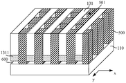
- a first isolation layer 500 is formed on the substrate 110 to fill the spacing between the active lines 131; the first isolation layer 500 is patterned, and the first isolation layer 500 is patterned between adjacent active lines 131 A plurality of openings 501 are formed in the first isolation layer 500 between, and the openings 501 expose the sacrificial layer 120a.
- the material of the first isolation layer 500 is different from that of the sacrificial layer 120 a, and the material of the first isolation layer 500 is an insulating material for providing electrical isolation between the active lines 131.
- the material of the first isolation layer 500 is silicon oxide.
- the method of forming the first isolation layer 500 is a chemical vapor deposition process, forming a filling space between adjacent active lines 131 and covering the top of the active lines 131 on the substrate 100 After the isolation material layer is formed, the isolation material layer is planarized to form the first isolation layer 500.
- the top of the first isolation layer 500 is flush with the top of the active line 131; in other specific embodiments, the top of the active line 131 is reserved for
- the layer is patterned to form a patterned mask layer for active lines, the first isolation layer 500 is flush with the patterned mask layer; in other specific embodiments, before the first isolation layer 500 is formed
- the patterned mask layer has been removed, and the first isolation layer 500 also covers the top of the active line. In the subsequent process, the top of the active line 131 can be protected.
- the isolation layer 500 is etched to form an opening 501.
- the sidewall of the opening 501 exposes the sidewall of the active line 131 and the sacrificial layer 120a. More than two openings 501 are formed between every two adjacent active lines 131.
- the bottom of the opening 501 may expose the substrate 100 or may be located in the sacrificial layer 120a, as long as the bottom of the opening 501 exposes at least a part of the sidewall of the sacrificial layer 120a.
- the opening 501 does not expose the sidewalls of the active lines 131, for example, the size of the opening 501 in the direction along the spacing between the active lines 131 is smaller than the length of the spacing between the active lines 131, In order to protect the active line.
- the isolation layer 500 is a multilayer dielectric layer.
- the silicon oxide is formed on the surface of the active line 131, the silicon nitride fills the space between the remaining active lines 131, and the opening 501 is formed in the nitrogen In silicon.
- the silicon oxide functions to protect the active line 131.
- the openings are also formed at the ends of the same side of each of the active lines, or the openings are formed at the ends of the two sides of each of the active lines, and each of the active lines
- the opening is formed on only one end of the source line, and the openings on the ends on the same side are distributed at intervals to reduce the density of the openings in a local area and increase the process window.
- a bit line connection line can be formed in the opening of the end portion at the same time, and the bit line connection line and the bit line are formed in the same process step to save process cost.
- the sacrificial layer 120 a is removed along the opening 501, and a gap 600 is formed between the bottom of the active line 131 and the substrate 110.
- the sacrificial layer 120a is removed by a wet etching process, and those skilled in the art can select an appropriate etching solution according to the material of the sacrificial layer 120a, so that during the wet etching process, the sacrificial layer 120a and the sacrificial layer 120a
- the active line 131 and the first isolation layer 500 have a higher etching selection ratio, so as to reduce the impact on the active line 131 and the first isolation layer 500 during the process of removing the sacrificial layer 120a .
- the active line 131 is supported by the first isolation layer 500 and suspended above the substrate 110 to form a gap 600 with the substrate 110.
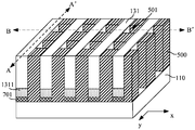
- FIGS. 7A-7C the gap 600 is filled with conductive material to form a bit line 701 extending in the first direction.
- FIG. 7B is a schematic cross-sectional view taken along the secant line A-A' in FIG. 7A
- FIG. 7C is an along view A schematic cross-sectional view of the secant line B-B' in 7A.
- a conductive material such as polysilicon or metal materials such as W, Co, Ag, or Al, can be deposited in the gap 600 by an atomic layer deposition process, a chemical vapor deposition process, or a physical vapor deposition process.
- the conductive material may also be a multilayer material, such as a combination of TiN and W.
- the conductive material fills the gap 600 to form a bit line 701 located at the bottom of the active line 131; the conductive material also fills the opening 501 and covers the first isolation layer 500 and the top of the active line 131 Afterwards, the conductive material on the top of the first isolation layer 500 and the top of the active line 131 is removed by etching back or planarization, and the conductive material of the opening 501 is removed by etching, so as to avoid adjacent active lines 131
- the bit lines 701 at the bottom are connected to each other.
- the bit line 701 may also be formed in the gap 600 by a selective growth technique.
- a bit line connection line 702 is formed at the end of the active line 131, and the bottom of the bit line connection line 702 is connected to the bit line 701.
- Fig. 8B is a schematic cross-sectional view along the cut line A-A' in Fig. 8A;
- Fig. 8C is a schematic cross-sectional view along the cut line B-B' in Fig. 8A.
- an opening exposing the bit line 701 is formed at the end of the active line 131; a conductive material is filled in the opening to form a bit line connection line 702.
- a conductive material is filled in the opening to form a bit line connection line 702.
- it further includes filling the opening 501 (please refer to FIG. 7A) with an insulating dielectric material and planarizing it to form the isolation dielectric layer 502.
- the surface of the isolation dielectric layer 502 is flush with the surface of the first isolation layer 500 or covers the entire first isolation layer 500 and the top of the active line 131.
- the isolation dielectric layer 502 is used to provide electrical isolation between adjacent active lines 131 and used to provide a flat surface to form a mask layer for etching the active lines 131 to form openings.
- the isolation dielectric layer 502 may not be formed.
- the opening 501 is filled with the material of the mask layer, such as the bottom anti-reflection layer. To form a flat surface.
- the opening is formed at the end of the active line 131; in other specific embodiments, the opening may also be formed at other positions of the active line 131.
- the end of the active line 131 is also formed with an opening 501.
- a mask is formed on the opening 501 at the end. Layer, the mask layer is used to prevent the removal of the conductive material in the opening 501 at the end of the active line 131 when the conductive material in the opening 501 is removed by etching, and the end opening of the active line 131 is used
- the conductive material remaining in 501 forms a bit line connection line 702.
- the bottom of the bit line connecting line 702 is connected to the bit line 701 and is used to lead out the bit line 701 buried under the active line 131 to facilitate the application of control signals to the bit line 701.
- the bit line 701 is located below the active line 131, forms an electrical connection with the first doped region 1311 at the bottom of the active line 131, and extends along the extending direction of the active line 131.
- FIG. 9 Please refer to FIG. 9 to pattern the active line 131 (refer to FIG. 8A) to form a number of discrete active pillars 132.
- the active line 131 is patterned through a selective etching process to form an active pillar 132.
- the active pillars 132 are arranged in an array along a first direction (y direction) and a second direction (x direction).
- first direction and the second direction form 90°; in other specific embodiments, the angle between the first direction and the second direction is 60° to 90°.
- ion implantation may be performed on the active pillar to form a channel region and a second doped region located above the channel region.
- the channel region is adjusted by ion implantation.
- the doping concentration inside is used to adjust the threshold voltage of the formed transistor.
- the channel region can be P-type or N-type doping. According to the requirements of the threshold voltage, an appropriate doping type and doping concentration are selected. In other specific embodiments, the channel region may not be doped.
- in-situ doping may also be used to form a doped channel layer in the active layer 130, After the active layer 130 is patterned to form the active pillar 132, the doped channel layer is patterned into a channel region.
- the second doped region may also be formed above the channel region by ion implantation; or in the process of forming the active layer 130, the second doped region may be formed at the corresponding position by in-situ doping. Two doped layers, so that after the active layer 130 is patterned to form the active pillars 132, the second doped layer is patterned into a second doped region.
- the active line may not be doped to form the first doped region 1311 in the foregoing step. Instead, after the active pillar 132 is formed in this step, the diffusion process or ion doped transition layer may be used.
- the first doped region at the bottom of the active pillar 132 is formed by implantation or the like.
- the first isolation layer 500 and the isolation dielectric layer 502 are etched back to expose a part of the height of the active pillars 132.
- the method further includes filling the openings between the adjacent active pillars 132 with isolation dielectric material, and at the same time, the first isolation layer 500 and the isolation dielectric layer
- the layer 502 and the isolation dielectric material are etched back to form a first isolation layer 500a, an isolation dielectric layer 502a, and an isolation dielectric layer 503 after the etch back, respectively, with a height equivalent to the first doped region 1311.
- the surfaces of the first isolation layer 500a, the isolation dielectric layer 502a, and the isolation dielectric layer 503 after the etch-back are flush with the top of the first doped region 1311.
- the surfaces of the first isolation layer 500a, isolation dielectric layer 502a, and isolation dielectric layer 503 may be slightly lower or slightly higher than the top boundary of the first doped region 1311, exposing the The active pillar 132 is located in an area above the first doped region 1311.
- a mask may be used to cover the bit line connection line 702 and a part of the first isolation layer 500 between the adjacent bit line connection lines 702, so that it is not It is etched to avoid damage to the bit line connection line 701.
- the first isolation layer 500 at each position may also be etched back.
- a gate dielectric layer and a gate electrode layer are sequentially formed on the first isolation layer 500a, isolation dielectric layer 502a, isolation dielectric layer 503, and exposed active pillars 132 after etch-back;
- the gate electrode layer is patterned to form a gate structure 1000 surrounding the channel region of the active pillar.
- the gate dielectric layer may be a gate dielectric material such as silicon oxide, silicon oxynitride, hafnium oxide, aluminum oxide, etc.; the material of the gate electrode layer may be a conductive material such as polysilicon, tungsten, or aluminum.
- the gate dielectric layer and the gate electrode layer covering the structure of FIG. 10 may be sequentially formed through a deposition process; then, through an etching process, the gate dielectric layer and the gate electrode layer are patterned to form the gate structure 1000 .
- the gate structure 1000 surrounds the channel region of the active pillar 132.
- the gate structure 1000 includes a gate dielectric layer and a gate electrode covering the gate dielectric layer. Only the gate electrode in the gate structure 1000 is shown in FIG. 11.
- the gate electrodes of the gate structures 1000 on the active pillars 132 on the same straight line arranged in the second direction (x direction) are connected to form a word line.
- the gate structures 1000 on each active pillar 132 may also be independent of each other.
- each gate structure 1000 After forming the gate structure 1000, it further includes filling an isolation dielectric layer 1001 between adjacent gate structures 1000.
- the isolation dielectric layer 1001 also covers the gate structure 1000 and the second doped region 1321.
- ion implantation is performed on the top region of the active pillar 132 to form the second doped region 1321.
- the doping type of the second doped region 1321 is the same as the doping type of the first doped region 1311, and the second doped region 1321 and the first doped region 1311 respectively serve as vertical transistors The source or drain.
- the second doped region 1321 can also be formed in the aforementioned steps by using a suitable in-situ doping, diffusion or implantation method, which will not be repeated here.
- a second isolation layer 1200 covering the gate structure 1000 and the second doped region 1321 is formed, and the second isolation layer 1200 exposes the bit line connection line 702 and the first The top surface of the second doped region 1321.
- Fig. 13B is a schematic cross-sectional view along the secant line A-A' in Fig. 13A
- Fig. 13C is a schematic cross-sectional view along the secant line C-C' in Fig. 13A.
- the material of the second isolation layer 1200 may be an insulating dielectric material such as silicon oxide, silicon oxynitride, etc.
- the second isolation layer 1200 and the first isolation layers 500, 500a and the isolation dielectric layers 502a, 1001 form respective vertical An isolation layer between type transistors and a flat surface for forming other semiconductor structures or material layers above the vertical type transistors.
- the above forming method forms a vertical transistor on a substrate, and forms a buried bit line between the first doped region at the bottom of the vertical transistor and the substrate, so that the area of the transistor can be reduced, and At the same time, the problem of how to apply the bit line signal to the vertical transistor is solved.
- FIG. 14 is a schematic structural diagram of the active line 131 in another specific embodiment based on FIG. 4 to form an opening 501'.
- the active lines 131 are patterned to form a number of active pillars 132' and a number of openings 501'.
- the sidewall of the opening 501' exposes the sacrificial layer 210a.
- the sacrificial layer 210a is removed along the opening 501', and a gap is formed between the bottom of the active pillar 132' and the substrate 110;
- the bit line 701' extending in one direction.
- conductive material will be filled in the opening 501', and a part of the thickness of the conductive material in the opening 501' can be removed by an etching process, leaving a portion of the thickness of the bottom of the opening 501' Conductive material to form a continuous bit line 701' at the bottom of the active pillars 132' on the same straight line arranged along the first direction.
- the opening 501' is also formed at the end of each active line 131 on the same side, or the opening is formed at the end of each active line 131 on both sides, and each The openings 501' are formed on only one end of each active line 131, and the openings on the ends on the same side are distributed at intervals to reduce the density of the openings in a local area and increase the process window.
- a bit line connection line can be formed in the opening of the end portion at the same time, and the bit line connection line and the bit line are formed in the same process step to save process cost.
- the specific embodiment of the present invention also provides a semiconductor structure.
- FIGS. 13A to 13C are schematic structural diagrams of a semiconductor structure according to a specific embodiment of the present invention.
- the semiconductor structure includes: a substrate 110; a vertical transistor located on the substrate 110; connected to the bottom of the vertical transistor and located between the bottom of the vertical transistor and the substrate 110 ⁇ 701 ⁇ The bit line 701. In this specific manner, the semiconductor structure is shown in FIGS. 13A to 13C.
- the semiconductor structure may be formed using the method in the above specific embodiments, or other methods may be used. All semiconductor structures with vertical transistors and buried bit lines located at the bottom of the vertical transistors can be used as the semiconductor structures claimed in this application.
- the vertical transistor includes a first doped region 1311, a channel region 1322, and a second doped region 1321 that are sequentially arranged in an upward direction from the substrate 110, and surround the channel region 1322.
- the gate structure 1000 is set.
- a plurality of the vertical transistors are formed on the semiconductor structure, which are arranged in an array along a first direction (y direction) and a second direction (x direction), and the bottoms of the vertical transistors on the same straight line arranged in the first direction
- the first doped region 1311 is connected to the same bit line 701; the gate structures 1000 of the vertical transistors on the same straight line arranged in the second direction are connected.
- the semiconductor structure further includes an isolation layer formed between the vertical transistors on the substrate 110, and the isolation layer includes an isolation layer located between the bit line 701 and the first doped region 1311 on different straight lines.
- the first isolation layer 500a, and the isolation dielectric layer 503 located between adjacent first doped regions 1311 on the same straight line, between the gate structure 1000 and located on the first isolation layer 500a and the isolation dielectric layer 503
- the semiconductor structure further includes an opening penetrating the active layer, a bit line connection line 702 is formed in the opening, and the bottom of the bit line connection line 702 is connected to the bit line 701.
- the bit line connection line 701 is located on both sides of the transistor array, and on each side of each row of transistors arranged in the y direction, a bit line connection line 702 and the bit line below the row of transistors are formed at intervals.
- the line 701 is connected, and a first isolation layer 500 is provided between adjacent bit line connection lines 702.
- the plurality of bit line connection lines are respectively located on the ends of the plurality of bit lines in a one-to-one correspondence, and the bit line connection lines are distributed at intervals at the ends of the bit lines.
- the bit line connection line and the bit line are formed in the same process step.
- the first doped region 1311, the channel region 1322, and the second doped region 1321 of the vertical transistor are located in the same active pillar, and the active pillar is an integral structure.
- the first doped region 1311, the channel region 1322, and the second doped region 1321 are formed by doping.
- in-situ doping may also be used to form a first doped layer and a doping trench in the active layer 130. The channel layer and the second doped layer.
- the first doped layer is patterned into a first doped region, and the doped channel layer It is patterned into a channel region, and the second doped layer is patterned into a second doped region.
- the channel region 1322 and the second doped region 1321 of the vertical transistor are formed in the epitaxial semiconductor column on the first doped region 1311, and the channel region 1322 and the second doped region 1311
- the semiconductor layer where the doped region 1321 is located and the epitaxial semiconductor pillar are not an integral structure, but are formed separately.
- the doped ions in the first doped region 1311 and/or the second doped region 1321 are formed by diffusion or ion implantation.
- the specific embodiment of the present invention also provides a memory and a method of forming the same.
- the semiconductor structure includes: a substrate; a vertical transistor located on the substrate; connected to the bottom of the vertical transistor and located between the bottom of the vertical transistor and the substrate Between the bit lines.
- the semiconductor structure is shown in FIGS. 13A to 13C.
- the semiconductor structure may be formed by the method in the above-mentioned specific embodiments, or other methods may be used. All semiconductor structures with vertical transistors and buried bit lines located at the bottom of the vertical transistors can be used as the semiconductor structures claimed in this application.
- a memory cell 1300 is formed above the vertical transistor, and the memory cell 1300 is electrically connected to the second doped region 1321 of the vertical transistor.
- the memory is a DRAM memory
- the memory unit 1300 is a capacitor, and includes an upper electrode, a lower electrode, and a capacitor dielectric layer located between the upper and lower electrodes.
- the structure of the capacitor may be a planar capacitor, a cylindrical capacitor, etc., and those skilled in the art can select a capacitor with a suitable structure as the storage unit according to requirements.
- the storage unit 1300 is only an example, and does not represent the actual structure of the capacitor.
- the second doped region 1321 of each transistor is connected to a memory cell to form a 1T1C memory structure.
- the storage unit may include one capacitor, or two or more capacitors connected in parallel.
- a metal contact layer may also be formed on the second doped region 1321, and then a metal contact layer may be formed on the second doped region 1321.
- the memory cell is formed on the metal contact layer.
- the memory cell 1300 is formed in a dielectric layer (not shown in the figure), and an interconnection structure connecting the bit line connecting line 701 and the gate structure 1000 may also be formed in the dielectric layer to connect the The bit line and the word line are connected to an external circuit.
- the memory cell may also be any of various memory cells such as a magnetic memory cell, a ferroelectric memory cell, a phase change memory cell, or a resistive memory cell.
- FIG. 17 is a schematic structural diagram of a memory according to a specific embodiment of the present invention.
- the memory is a FeRAM memory, and an electrically connected ferroelectric memory cell 1400 is formed above the second doped region 1321 of the vertical transistor of the semiconductor structure shown in FIG. 13A.
- the ferroelectric memory cell includes a lower electrode connected to the second doped region 1321, an upper electrode located above the lower electrode, and a layer of ferroelectric material between the upper and lower electrodes. Ferroelectric capacitors.
- the material of the ferroelectric material layer may be PZT (lead zirconate titanate) or SBT (barium strontium titanate).
- the ferroelectric memory cell 1400 in FIG. 17 is only for illustration, and does not represent the actual structure of the ferroelectric memory cell. Those skilled in the art should be able to combine as needed to form a ferroelectric memory cell 1400 with a corresponding structure, which is not limited here.
- the ferroelectric memory cell 1400 it is also necessary to form a plate line 1401 connected to the upper electrode above the ferroelectric memory cell 1400.
- the ferroelectric memory cells arranged in the second direction (x direction) on the same straight line are electrically connected to the same plate line 1401, and the plate line 1401 and the vertical transistors below can be realized Bidirectional pressure is applied to the ferroelectric memory cell 1400, thereby utilizing the properties of the ferroelectric material layer for data storage.
- a magnetic memory cell may also be formed on the second doped region 1321 of the vertical transistor, the magnetic memory cell includes a magnetic tunnel junction, and the magnetic tunnel junction includes a fixed layer, a free layer, and A dielectric layer located between the fixed layer and the free layer.
- the fixed layer is connected to the second doped region 1321.
- vertical transistors are used as the control transistors connected to the memory cell, and the buried bit lines connected to the control transistors can increase the storage density of the memory.
Landscapes
- Engineering & Computer Science (AREA)
- Power Engineering (AREA)
- Manufacturing & Machinery (AREA)
- Physics & Mathematics (AREA)
- Condensed Matter Physics & Semiconductors (AREA)
- General Physics & Mathematics (AREA)
- Computer Hardware Design (AREA)
- Microelectronics & Electronic Packaging (AREA)
- Semiconductor Memories (AREA)
Abstract
本发明涉及一种半导体结构及其形成方法,一种存储器及其形成方法,所述半导体结构包括:衬底;位于所述衬底上的竖直型晶体管;与所述竖直型晶体管底部连接,且位于所述竖直型晶体管底部与所述衬底之间的位线。所述半导体结构内的竖直晶体管的平面尺寸较小。
Description
相关申请引用说明
本申请要求于2020年04月27日递交的中国专利申请号202010343497.2,申请名为“半导体结构及其形成方法、存储器及其形成方法”的优先权,其全部内容以引用的形式附录于此。
本发明涉及半导体技术领域,尤其涉及一种半导体结构及其形成方法、存储器及其形成方法。
现有的存储器通常包括数据存储单元以及控制所述数据存储单元的控制晶体管。晶体管的集成度制约了存储器的存储密度。对于平面晶体管,现有技术通过缩小晶体管的沟道尺寸来减小晶体管的尺寸,从而提高存储器的存储密度。
但是随着晶体管沟道尺寸的减小,窄沟道效应以及短沟道效应所导致晶体管性能下降,使得存储器的性能受到影响,制约了晶体管尺寸以及存储器存储密度的进一步提高。
如何在不降低晶体管性能的前提下,减小晶体管的平面尺寸,提高存储器的存储密度是目前亟待解决的问题。
发明内容
本发明所要解决的技术问题是,提供一种半导体结构及其形成方法、存储器及其形成方法,进一步提高存储器的存储密度。
为了解决上述问题,本发明提供了一种半导体结构,包括:衬底;
位于所述衬底上的竖直型晶体管;与所述竖直型晶体管底部连接,且位于所述竖直型晶体管底部与所述衬底之间的位线。
可选的,所述竖直型晶体管包括:自衬底向上的方向上依次设置的第一掺杂区、沟道区、第二掺杂区以及环绕所述沟道区设置的栅极结构。
可选的,所述衬底上形成有多个所述竖直型晶体管,沿第一方向和第二方向阵列分布,沿第一方向排列的同一直线上的竖直型晶体管底部的第一掺杂区连接至同一位线;沿第二方向排列的同一直线上的竖直型晶体管的栅极结构相连接。
可选的,还包括:位于所述衬底上形成于各竖直型晶体管之间的隔离层,所述隔离层包括至少一层绝缘介质层。
可选的,还包括:位线连接线,所述位线连接线底部连接至所述位线。
可选的,所述竖直晶体管的第一掺杂区、沟道区、第二掺杂区位于同一有源柱内;或者,所述竖直晶体管的沟道区和第二掺杂区形成于所述第一掺杂区上的外延半导体柱内。
可选的,所述第一掺杂区和/或所述第二掺杂区内的掺杂离子通过扩散或离子注入方式形成。
可选的,所述位线连接线与所述位线在同一工艺步骤中形成。
可选的,多个所述位线连接线分别一一对应的位于多个所述位线的端部上,并且所述 位线连接线在所述位线的端部间隔分布。
本发明的技术方案还提供一种半导体结构的形成方法,包括:提供衬底,所述衬底上形成有牺牲层和位于所述牺牲层上的有源层;
对所述有源层进行图形化,形成暴露出所述牺牲层的开口;利用所述开口去除所述牺牲层;在所述牺牲层的部分位置处形成位线。
可选的,对所述有源层进行图形化,形成所述有源柱;在所述有源柱的底部与所述衬底之间形成所述位线。
可选的,还包括:形成位于所述有源柱底部向上依次设置的第一掺杂区、沟道区、第二掺杂区,以及形成环绕所述沟道区的栅极结构。
可选的,所述第一掺杂区、沟道区、第二掺杂区的形成方法包括:采用原位掺杂工艺,在采用外延生长工艺形成所述有源层的过程中,对所述有源层进行掺杂,依次形成第一掺杂层、沟道掺杂层以及第二掺杂层;在图形化所述有源层形成所述有源柱后,所述第一掺杂层、沟道掺杂层以及第二掺杂层分别被图形化为自有源柱底部向上依次设置的所述第一掺杂区、所述沟道区以及所述第二掺杂区。
可选的,所述第一掺杂区的形成方法包括:在形成所述有源柱之后,在相邻有源柱之间的衬底上形成具有掺杂元素的过渡层;通过扩散处理,将过渡层内的至少部分掺杂元素扩散进入有源柱内,形成所述第一掺杂区。
可选的,所述第一掺杂区和所述第二掺杂区的形成方法包括:对所述有源柱的底部区域进行离子注入,形成位于所述有源柱底部的所述第一掺杂区;对所述有源柱的顶部区域进行离子注入,形成位于所述有源柱顶部的所述第二掺杂区。
可选的,对所述有源层进行图形化,形成有源柱;在所述有源柱的底部与所述衬底之间形成所述位线的方法进一步包括:刻蚀所述有源层和所述牺牲层,形成沿第一方向延伸的有源线;形成填充各有源线之间间距的第一隔离层;对所述有源线进行图形化,形成若干有源柱及若干开口,所述开口暴露出所述牺牲层;利用所述开口去除所述牺牲层,在所述有源柱底部与所述衬底之间形成间隙;在所述间隙内填充导电材料,形成沿第一方向延伸的所述位线。
可选的,对所述有源层进行图形化,形成有源柱;在所述有源柱的底部与所述衬底之间形成所述位线的方法进一步包括:刻蚀所述有源层和所述牺牲层,形成沿第一方向延伸的有源线;形成填充各有源线之间间距的第一隔离层;对所述第一隔离层进行图形化,在所述第一隔离层内形成若干开口,所述开口暴露出所述牺牲层;利用所述开口去除所述牺牲层,在所述有源线底部与所述衬底之间形成间隙;在所述间隙内填充导电材料,形成沿第一方向延伸的所述位线;对所述有源线进行图形化,形成沿第一方向和第二方向阵列排布的有源柱。
可选的,还包括:在所述有源线端部形成开口;在所述开口内填充导电材料,形成位线连接线,所述位线连接线底部与所述位线连接。
可选的,在同一工艺步骤中形成所述位线连接线和所述位线。
可选的,还包括:回刻蚀所述第一隔离层,暴露出部分高度的有源柱;在回刻蚀后的暴露的有源柱上依次形成栅介质层以及栅电极层;对所述栅介质层和所述栅电极层进行图形化,形成环绕所述有源柱的沟道区的栅极结构,并暴露出所述有源柱的顶部区域。
本发明的技术方案还提供一种存储器,包括:如上述任一项所述的半导体结构;位于所述竖直型晶体管上方的存储单元,所述存储单元电连接至所述竖直型晶体管的顶部。
可选的,所述存储单元包括电容存储单元、磁性存储单元、铁电存储单元、相变存储单元或者电阻存储单元中的任一种。
本发明的技术方案还提供存储器的形成方法,包括:提供如上述任一项所述的半导体结构;在所述竖直型晶体管上方形成存储单元,所述存储单元电连接至所述竖直型晶体管的顶部。
可选的,所述存储单元包括电容存储单元、磁性存储单元、铁电存储单元、相变存储单元或者电阻存储单元。
本发明的半导体结构的形成方法,在衬底上形成牺牲层以及位于牺牲层上的有源层,利用位线替代牺牲层的位置,从而形成埋入式的位线,从而便于后续形成竖直型的晶体管,通过位线将竖直型的晶体管底部的源/漏极引出。
进一步的,竖直型的晶体管占据的版图尺寸较小,且沟道长度由有源层的厚度来决定,可以在不减小沟道长度等情况下,减小晶体管的面积,从而提高半导体结构的集成度。
进一步的,通过形成多个开口,利用多个开口去除牺牲层,可以提高去除牺牲层的效率,避免牺牲层的残留,从而提高形成的位线的质量。
本发明的存储器包括具有竖直型晶体管阵列的半导体结构,在晶体管尺寸较小的情况下,能够提高存储器的存储密度。
图1至图13C为本发明一具体实施方式的半导体形成过程的结构示意图;
图14至图15为本发明一具体实施方式的半导体形成过程的结构示意图;
图16为本发明一具体实施方式的存储器的结构示意图;
图17为本发明一具体实施方式的存储器的结构示意图。
下面结合附图对本发明提供的半导体结构及其形成方法、存储器及其形成方法的具体实施方式做详细说明。
请参考图1至图13C,为本发明一具体实施方式的半导体形成过程的结构示意图。
请参考图1,提供衬底110,所述衬底110上形成有牺牲层120和位于所述牺牲层120上的有源层130。
所述衬底110可以为Si、Ge、SiC等,各种半导体材料,可以为单层结构也可以为复合结构,在此不作限定。
可以通过沉积或其他工艺在所述衬底110上依次形成所述牺牲层120和所述有源层130。所述有源层130采用半导体材料,例如Si、Ge或SiC等,可以是其中的一种或多种 半导体材料。所述牺牲层120的材料与所述衬底110、有源层130的材料不同,使得后续在去除所述牺牲层120的过程中,减少对所述衬底110、有源层130的影响。
该具体实施方式中,所述衬底110为硅衬底,所述牺牲层120为SiGe层,所述有源层为硅层。采用外延生长工艺,在所述衬底110上外延形成所述牺牲层120之后,再通过外延工艺,在所述牺牲层120上形成有源层130。
实际上,所述牺牲层120只要与所述衬底110以及有源层130采用不同的材料,在去除牺牲层120的过程中,牺牲层120与所述衬底110以及有源层130之间有刻蚀选择比即可。
在一些具体实施方式中,所述衬底110、牺牲层120以及有源层130可以为SOI结构,其中SOI结构中的埋氧层作为牺牲层120。
在其他具体实施方式中,可以通过对体硅衬底进行离子注入,在所述体硅衬底内部形成掺杂层作为所述牺牲层120。例如对体硅进行Ge注入,通过控制Ge的注入深度,在体硅内部形成SiGe层作为牺牲层120,掺杂层下方的硅层为衬底110,掺杂层上方的硅层作为有源层。在其他具体实施方式中,也可以通过注入其他元素形成所述掺杂层,例如C、O、N等,使得所述掺杂层的刻蚀速率与其上方及下方的材料层均不同,从而形成所述牺牲层120。较佳的,所述牺牲层120的材料可以为氧化硅、氮化硅、氮氧化硅、碳氧化硅等。
所述有源层130用于形成竖直晶体管,所述牺牲层120用于后续被替代形成位线。根据待形成的竖直晶体管的尺寸以及位线的尺寸,合理设置所述牺牲层120和所述有源层130的厚度。在一个具体实施方式中,所述牺牲层120的厚度可以为35nm~50nm,所述有源层130的厚度可以为100nm~1000nm。
请参考图2,刻蚀所述有源层130和所述牺牲层120至所述衬底110,形成若干平行排列的沿第一方向延伸的有源线131。
该具体实施方式中,形成所述有源线131的方法进一步包括:在所述有源层130上形成图形化掩膜层(图中未示出),所述图形化掩膜层内具有沿第一方向延伸的开口图形;以所述图形化掩膜层为掩膜,刻蚀所述有源层130和所述牺牲层120,形成长条状的有源线131以及长条状的牺牲层120a。
该具体实施方式中,所述第一方向为y方向。采用干法刻蚀工艺刻蚀所述有源层130和所述牺牲层120,在相应的刻蚀阶段,选择对应的刻蚀气体,对所述有源层130和所述牺牲层120进行刻蚀。
请参考图3,在相邻有源线131之间的衬底110上形成具有掺杂元素的过渡层310。
可以通过在衬底100上沉积过渡层材料后,进行回刻蚀,形成一定厚度的过渡层310。所述过渡层310的厚度可以根据待形成的晶体管的源/漏区的尺寸要求调整。
所述过渡层310的材料与所述有源线131的材料不同,可以为利于杂质扩散的材料,例如多晶硅,还可以为其他材料例如氧化硅、氮化硅、氮氧化硅等介质材料。
形成具有掺杂元素的所述过渡层310的形成方法包括:在衬底110上形成一定厚度未被掺杂的过渡层310之后,通过离子注入,对所述过渡层310进行掺杂。此时,在所述有 源线131顶部覆盖有图形化掩膜层,通过控制所述离子注入的能量,使得所述离子注入仅能对所述过渡层310进行掺杂。根据待形成的晶体管的类型,向所述过渡层310内注入N型或P型离子,或者具有N型或P型离子的原子团簇。所述过渡层310内的掺杂元素可以以离子、原子、化合物分子或者团簇形式存在。
在其他具体实施方式中,也可以在形成所述过渡层310的过程中,通过原位掺杂工艺,通过在沉积工艺气体中加入具有掺杂元素的掺杂气体,直接形成具有掺杂元素的过渡层310。
请参考图4,通过扩散处理,将具有掺杂原子的过渡层310内的至少部分掺杂元素扩散进入有源线131内,形成所述第一掺杂区1311。
所述扩散处理可以为热退火工艺,根据掺杂原子的扩散效率,选择合适参数的退火工艺,使得所述过渡层310内的掺杂元素扩散进入所述有源线131内,形成与所述过渡层310厚度相当的第一掺杂区1311。
可以通过调整所述过渡层310内的掺杂元素的浓度,扩散处理时间、温度等参数,调整扩散处理后形成的第一掺杂区1311内的掺杂浓度。
在其他具体实施方式中,也可以在去除有源线131顶部的图形化掩膜层之后,直接通过对所述有源线131进行掺杂离子注入,形成所述第一掺杂区1311,具体的,通过控制离子注入过程的注入离子的能量和方向,调整注入深度,在所述有源线131的底部形成所述第一掺杂区1311。
在其他具体实施方式中,也可以在后续其他步骤中,例如后续对有源线进行图形化,进一步形成有源柱后或其他步骤中,通过离子注入方式在有源线或有源柱底部形成第一掺杂区。
在其他具体实施方式中,还可以采用原位掺杂工艺,在通过外延工艺沉积形成所述有源层的过程中,对所述有源层进行掺杂,形成位于有源层底部的第一掺杂层;在对有源层进行图形化后,形成位于有源线或有源柱底部的第一掺杂区。
请参考图5,在所述衬底110上形成填充各有源线131之间间距的第一隔离层500;对所述第一隔离层500进行图形化,在相邻的有源线131之间的第一隔离层500内形成若干开口501,所述开口501暴露出所述牺牲层120a。
所述第一隔离层500的材料与所述牺牲层120a不同,且所述第一隔离层500的材料为绝缘材料,用于在各有源线131之间提供电学隔离。该具体实施方式中,所述第一隔离层500的材料为氧化硅。该具体实施方式中,形成所述第一隔离层500的方法为化学气相沉积工艺,在所述衬底100上形成填充相邻有源线131之间的间距以及覆盖所述有源线131顶部的隔离材料层之后,对隔离材料层进行平坦化,形成所述第一隔离层500。该具体实施方式中,所述第一隔离层500的顶部与所述有源线131的顶部齐平;在其他具体实施方式中,所述有源线131顶部还保留有用于对由于对有源层进行图形化形成有源线的图形化掩膜层,所述第一隔离层500与所述图形化掩膜层齐平;在其他具体实施方式中,在形成所述第一隔离层500之前,所述图形化掩膜层已被去除,所述第一隔离层500还覆盖所述有源线的 顶部,在后续工艺中,可以对所述有源线131顶部进行保护。
在形成所述隔离层500之后,对所述隔离层500进行刻蚀,形成开口501。所述开口501的侧壁暴露出所述有源线131以及牺牲层120a的侧壁。每两个相邻的有源线131之间,均形成有两个以上的所述开口501。具体的,所述开口501的底部可以暴露所述衬底100,也可以位于所述牺牲层120a中,只要所述开口501的底部至少暴露所述牺牲层120a的部分侧壁即可。
在其他实施例中,所述开口501不暴露所述有源线131的侧壁,例如开口501在沿着有源线131之间间距方向上的尺寸小于有源线131之间间距的长度,以起到对有源线的保护。优选的,所述隔离层500为多层介质层。例如氧化硅和氮化硅的组合层,所述氧化硅形成于所述有源线131的表面,所述氮化硅填充剩余的有源线131之间的间距,开口501形成在所述氮化硅中。所述氧化硅起到保护有源线131的作用。
在其他实施例中,所述开口还形成在各所述有源线的同一边的端部,或者所述开口形成在各所述有源线两边的端部上,并且,每个所述有源线只有一个端部上形成所述开口,同一边的所述端部上的开口间隔分布,以减少局部区域上的所述开口的密度,以增大工艺窗口。在后续填充导电材料形成位线时,可同时在所述端部的开口中形成位线连接线,所述位线连接线与所述位线在同一工艺步骤中形成,以节约工艺成本。
请参考图6,沿所述开口501去除所述牺牲层120a,在所述有源线131底部与所述衬底110之间形成间隙600。
采用湿法刻蚀工艺去除所述牺牲层120a,本领域技术人员可以根据所述牺牲层120a的材料选择合适的刻蚀溶液,使得所述湿法刻蚀过程中,所述牺牲层120a和所述有源线131、第一隔离层500有较高的刻蚀选择比,以在去除所述牺牲层120a的过程中,减少对所述有源线131和所述第一隔离层500的影响。
在去除所述牺牲层120a之后,所述有源线131由所述第一隔离层500支撑,悬空于所述衬底110上方,与衬底110之间形成间隙600。
请参考图7A~7C,在所述间隙600内填充导电材料,形成沿第一方向延伸的位线701,图7B为沿图7A中割线A-A’的剖面示意图,图7C为沿图7A中割线B-B’的剖面示意图。
可以通过原子层沉积工艺或化学气相沉积或物理气相沉积工艺等方法在所述间隙600内沉积导电材料,例如多晶硅或者W、Co、Ag或Al等金属材料。所述导电材料也可以为多层材料,例如TiN和W的组合等。
所述导电材料填充所述间隙600,形成位于所述有源线131底部的位线701;所述导电材料还填充所述开口501,并覆盖所述第一隔离层500以及有源线131顶部,后续通过回刻蚀或者平坦化处理,去除所述第一隔离层500顶部以及有源线131顶部的导电材料以及通过刻蚀处理去除所述开口501的导电材料,避免相邻有源线131底部的位线701之间相互连接。也可以通过选择性生长技术在所述间隙600中形成所述位线701。
请参考图8A至图8C,在所述有源线131端部形成位线连接线702,所述位线连接线702底部与所述位线701连接。其中图8B为沿图8A中割线A-A’的剖面示意图;图8C为 沿图8A中割线B-B’的剖面示意图。
具体的,在所述有源线131端部形成暴露出所述位线701的开口;在所述开口内填充导电材料形成位线连接线702。在刻蚀形成所述开口之前,还包括在所述开口501(请参考图7A)内填充绝缘介质材料,并进行平坦化,形成所述隔离介质层502。所述隔离介质层502的表面与所述第一隔离层500的表面齐平或者覆盖整个所述第一隔离层500以及有源线131顶部。所述隔离介质层502用于提供相邻有源线131之间的电学隔离,并用于提供平坦表面,以形成用于刻蚀有源线131形成开口的掩膜层。
在其他具体实施方式中,也可以不形成所述隔离介质层502,在刻蚀有源线131的过程中,通过掩膜层的材料,例如底部抗反射层等将所述开口501填满,以形成平坦表面。
该具体实施方式中,在所述有源线131的端部形成所述开口;在其他具体实施方式中,也可以在所述有源线131的其他位置处形成所述开口。
在其他具体实施方式中,所述有源线131的端部也形成有开口501,在位线704的形成过程中,导电材料填充开口501之后,在所述端部的开口501上形成掩膜层,利用所述掩膜层阻止在刻蚀去除所述开口501中的导电材料时对所述有源线131端部的开口501中导电材料的去除,利用所述有源线131端部开口501中保留的导电材料形成位线连接线702。
位线连接线702的底部与所述位线701连接,用于将埋入所述有源线131下方的位线701引出,便于向所述位线701施加控制信号。所述位线701位于所述有源线131下方,与所述有源线131底部的第一掺杂区1311之间形成电连接,沿所述有源线131的延伸方向延伸。
请参考图9,对所述有源线131(请参考图8A)进行图形化,形成若干分立的有源柱132。
通过选择性刻蚀工艺,对所述有源线131进行图形化,形成有源柱132。所述有源柱132沿第一方向(y方向)和第二方向(x方向)阵列排布。该具体实施方式中,所述第一方向和第二方向之间成90°;在其他具体实施方式中,所述第一方向和第二方向之间的夹角为60°~90°。
在其他具体实施方式中,可以在形成所述有源柱132之后,对所述有源柱进行离子注入形成沟道区以及位于所述沟道区上方的第二掺杂区。
该具体实施方式中,在形成所述有源柱132之后,仅通过离子注入,在所述有源柱132底部的第一掺杂区1311上方,形成沟道区,通过离子注入调整沟道区内的掺杂浓度,以调整形成的晶体管的阈值电压,所述沟道区内可以为P型或N型掺杂,根据阈值电压的要求,选择合适的掺杂类型以及掺杂浓度。在其他具体实施方式中,也可以不用对沟道区进行掺杂。
在其他具体实施方式中,在前述形成有源层130(请参考图1)的过程中,也可以通过原位掺杂,在所述有源层130内形成有掺杂沟道层,在对有源层130进行图形化形成有源柱132后,所述掺杂沟道层被图形化为沟道区。
本发明的具体实施方式中,还可以通过离子注入,在所述沟道区上方形成第二掺杂区; 或者在形成有源层130的过程中,通过原位掺杂在对应位置处形成第二掺杂层,从而在对所述有源层130进行图形化形成有源柱132后,所述第二掺杂层被图形化为第二掺杂区。
在其他具体方式中,也可以在前述步骤中不对有源线进行掺杂形成第一掺杂区1311,而是在这一步骤形成有源柱132之后,通过掺杂过渡层的扩散处理或离子注入等方式形成有源柱132底部的第一掺杂区。
请参考图10,回刻蚀所述第一隔离层500和隔离介质层502,暴露出部分高度的有源柱132。
在回刻蚀所述第一隔离层500和隔离介质层502之前,还包括在相邻的有源柱132之间的开口内填充隔离介质材料,同时对所述第一隔离层500、隔离介质层502以及所述隔离介质材料进行回刻蚀,分别形成回刻蚀后的第一隔离层500a、隔离介质层502a以及隔离介质层503,高度与所述第一掺杂区1311相当。该具体实施方式中,回刻蚀后的第一隔离层500a、隔离介质层502a、隔离介质层503的表面与所述第一掺杂区1311的顶部齐平。在其他具体实施方式中,所述第一隔离层500a、隔离介质层502a、隔离介质层503的表面可以略低于或略高于所述第一掺杂区1311的顶部边界,暴露出所述有源柱132位于所述第一掺杂区1311上方的区域。
在对所述第一隔离层500进行回刻蚀的过程中,可以通过掩膜覆盖所述位线连接线702以及相邻位线连接线702之间的部分第一隔离层500,使其不被刻蚀,避免对所述位线连接线701造成损伤。
在其他具体实施方式中,也可以对各位置处的第一隔离层500均进行回刻蚀。
请参考图11,在回刻蚀后的第一隔离层500a、隔离介质层502a、隔离介质层503以及暴露的有源柱132上依次形成栅介质层以及栅电极层;对所述栅介质层和所述栅电极层进行图形化,形成环绕所述有源柱的沟道区的栅极结构1000。
所述栅介质层可以为氧化硅、氮氧化硅、氧化铪、氧化铝等栅介质材料;所述栅电极层的材料可以为多晶硅、钨或铝等导电材料。可以通过沉积工艺,依次形成覆盖所述图10结构上的栅介质层以及栅电极层;然后通过刻蚀工艺,随所述栅介质层和栅电极层进行图形化,形成所述栅极结构1000。所述栅极结构1000环绕有源柱132的沟道区。所述栅极结构1000包括栅介质层以及覆盖所述栅介质层的栅电极,图11中仅示出了所述栅极结构1000内的栅电极。
该具体实施方式中,沿第二方向(x方向)排列的同一直线上的有源柱132上的栅极结构1000的栅电极相连接,构成字线。
在其他具体实施方式中,各个有源柱132上的栅极结构1000之间也可以是相互独立的。
为了使得各栅极结构1000之间进行电学隔离,在形成所述栅极结构1000之后,还包括在相邻栅极结构1000之间填充隔离介质层1001。在其他具体实施方式中,所述隔离介质层1001还覆盖所述栅极结构1000和所述第二掺杂区1321。
请参考图12,形成所述栅极结构1000之后,对所述有源柱132的顶部区域进行离子注入,形成所述第二掺杂区1321。
所述第二掺杂区1321的掺杂类型与所述第一掺杂区1311的掺杂类型一致,所述第二掺杂区1321和所述第一掺杂区1311分别作为竖直型晶体管的源极或漏极。在其他具体实施方式中,所述第二掺杂区1321还可以在前述的步骤中,采用合适的原位掺杂、扩散或者注入方式形成,在此不再赘述。
请参考图13A至图13C,形成覆盖所述栅极结构1000、第二掺杂区1321的第二隔离层1200,所述第二隔离层1200暴露出所述位线连接线702和所述第二掺杂区1321的顶部表面。图13B为沿图13A中割线A-A’的剖面示意图,图13C为沿图13A中割线C-C’的剖面示意图。
所述第二隔离层1200的材料可以为氧化硅、氮氧化硅等绝缘介质材料,所述第二隔离层1200与所述第一隔离层500、500a以及隔离介质层502a、1001形成各竖直型晶体管之间的隔离层,并且为在所述竖直型晶体管上方形成其他半导体结构或材料层提供平坦表面。
上述形成方法在衬底上形成竖直型晶体管,且在所述竖直型晶体管底部的第一掺杂区下方与衬底之间形成埋入式的位线,从而可以减少晶体管的面积,并同时解决了如何对竖直晶体管的施加位线信号的问题。
在其他具体实施方式中,还可以通过对图4中有源线131进行图形化,形成有源柱之后,再去除所述牺牲层,形成位线。
请参考图14,为另一具体实施方式中,在图4基础上,对所述有源线131进行图形化,以形成开口501’的结构示意图。在所述衬底上形成填充各有源线131之间间距的第一隔离层500之后,对所述有源线131进行图形化,形成若干有源柱132’及若干开口501’,所述开口501’侧壁暴露出所述牺牲层210a。
请参考图15,沿所述开口501’去除所述牺牲层210a,在所述有源柱132’底部与所述衬底110之间形成间隙;在所述间隙内填充导电材料,形成沿第一方向延伸的所述位线701’。在形成所述位线701’的过程中,导电材料会填充于所述开口501’中,可以通过刻蚀工艺去除所述开口501’内部分厚度的导电材料,保留开口501’底部部分厚度的导电材料,以形成沿第一方向排列的同一直线上的有源柱132’底部的连续的位线701’。
在其他实施例中,所述开口501’还形成在各所述有源线131的同一边的端部,或者所述开口形成在各所述有源线131两边的端部上,并且,每个所述有源线131只有一个端部上形成所述开口501’,同一边的所述端部上的开口间隔分布,以减少局部区域上的所述开口的密度,以增大工艺窗口。在后续填充导电材料形成位线时,可同时在所述端部的开口中形成位线连接线,所述位线连接线与所述位线在同一工艺步骤中形成,以节约工艺成本。
后续可以采用上述具体实施方式中,如图8A以及后续的步骤,形成如图13A所示的半导体结构。与图8A相比,由于开口的位置发生变化,因此填充所述开口的隔离介质层的位置也发生变化,本领域技术人员可以根据需要对上述具体实施方式中部分步骤进行适应性的调整,均在本申请的保护范围内。
本发明的具体实施方式还提供一种半导体结构。
请参考图13A至图13C,为本发明一具体实施方式的半导体结构的结构示意图。
所述半导体结构包括:衬底110;位于所述衬底110上的竖直型晶体管;与所述竖直型晶体管底部连接,且位于所述竖直型晶体管底部与所述衬底110之间的位线701。该具体方式中,所述半导体结构如图13A至13C所示。
在本发明的其他具体实施方式中,所述半导体结构可以采用上述具体实施方式中的方法形成,也可以采用其他方法。所有具有竖直晶体管,以及位于竖直晶体管底部的埋入式位线的半导体结构,均可以作为本申请所要求保护的半导体结构。
该具体实施方式中,所述竖直型晶体管包括自衬底110向上的方向上依次设置的第一掺杂区1311、沟道区1322、第二掺杂区1321以及环绕所述沟道区1322设置的栅极结构1000。
所述半导体结构上形成有多个所述竖直型晶体管,沿第一方向(y方向)和第二方向(x方向)阵列分布,沿第一方向排列的同一直线上的竖直型晶体管底部的第一掺杂区1311连接至同一位线701;沿第二方向排列的同一直线上的竖直型晶体管的栅极结构1000相连接。
所述半导体结构还包括:位于所述衬底110上形成于各竖直型晶体管之间的隔离层,所述隔离层包括位于不同直线上的位线701、第一掺杂区1311之间的第一隔离层500a,以及位于同一直线上的相邻第一掺杂区1311之间的隔离介质层503、栅极结构1000之间且位于所述第一隔离层500a、隔离介质层503上的隔离介质层1001,以及位于所述隔离介质层1001上,相邻第二掺杂区1321之间的第二隔离层1200、与所述第一隔离层500a位于同一层内的隔离介质层502a。
所述半导体结构还包括:贯穿所述有源层的开口,所述开口内形成有位线连接线702,所述位线连接线702底部连接至所述位线701。该具体实施方式中,所述位线连接线701位于晶体管阵列的两侧边缘,沿y方向排列的每一行晶体管的每一侧,均间隔形成有位线连接线702与该行晶体管下方的位线701连接,相邻位线连接线702之间具有第一隔离层500。具体的,多个所述位线连接线分别一一对应的位于多个所述位线的端部上,并且所述位线连接线在所述位线的端部间隔分布。所述位线连接线与所述位线在同一工艺步骤中形成。
在一些具体实施方式中,所述竖直晶体管的第一掺杂区1311、沟道区1322、第二掺杂区1321位于同一有源柱内,所述有源柱为一体结构。通过掺杂形成了所述第一掺杂区1311、沟道区1322、第二掺杂区1321。在其他具体实施方式中,在形成有源层130(请参考图1)的过程中,也可以通过原位掺杂,在所述有源层130内形成有第一掺杂层、掺杂沟道层和第二掺杂层,在对所述有源层130进行图形化形成有源柱后,所述第一掺杂层被图形化为第一掺杂区,所述掺杂沟道层被图形化为沟道区,所述第二掺杂层被图形化为第二掺杂区。在其他具体实施方式中,所述竖直晶体管的沟道区1322和第二掺杂区1321形成于所述第一掺杂区1311上的外延半导体柱内,所述沟道区1322和第二掺杂区1321所在的半导体层和所述外延半导体柱非一体结构,而是分开形成的。
所述第一掺杂区1311和/或所述第二掺杂区1321内的掺杂离子通过扩散或离子注入方式形成。
本发明的具体实施方式还提供一种存储器及其形成方法。
首先提供半导体结构,所述半导体结构包括:衬底;位于所述衬底上的竖直型晶体管; 与所述竖直型晶体管底部连接,且位于所述竖直型晶体管底部与所述衬底之间的位线。该具体方式中,所述半导体结构如图13A至13C所示。所述半导体结构可以采用上述具体实施方式中的方法形成,也可以采用其他方法。所有具有竖直晶体管,以及位于竖直晶体管底部的埋入式位线的半导体结构,均可以作为本申请所要求保护的半导体结构。
请参考图16,在所述竖直型晶体管上方形成存储单元1300,所述存储单元1300电连接至所述竖直型晶体管的第二掺杂区1321。
在一个具体实施方式中,所述存储器为DRAM存储器,所述存储单元1300为电容器,包括上电极、下电极以及位于上、下电极之间的电容介质层。所述电容器的结构可以为平面电容器、柱形电容器等,本领域技术人员可以根据需求,选择合适结构的电容器作为存储单元。图16中,所述存储单元1300仅为示例,并不代表电容器的实际结构。该具体实施方式中,每个晶体管的第二掺杂区1321连接至一个存储单元,构成1T1C的存储结构。所述存储单元可以包括一个电容器,或两个以上并联的电容器。
在其他具体实施方式中,为了降低所述第二掺杂区1321与所述存储单元1300之间的连接电阻,还可以在所述第二掺杂区1321上形成金属接触层,然后再在所述金属接触层上形成所述存储单元。
所述存储单元1300形成于介质层(图中未示出)内,还可以在所述介质层内形成连接所述位线连接线701以及栅极结构1000的互连结构,用于将所述位线以及字线连接至外部电路。
在本发明的其他具体实施方式中,所述存储单元还可以为磁性存储单元、铁电存储单元、相变存储单元或者电阻存储单元等各种存储单元中的任一种。
请参考图17,为本发明一具体实施方式的存储器的结构示意图。
所述存储器为FeRAM存储器,在图13A所示的半导体结构的竖直型晶体管的第二掺杂区1321上方形成电连接的铁电存储单元1400。
所述铁电存储单元包括与所述的第二掺杂区1321连接的下电极、位于所述下电极上方的上电极、以及位于所述上、下电极之间的铁电材料层所构成的铁电电容。所述铁电材料层的材料可以为PZT(锆钛酸铅)或SBT(钛酸钡锶)。图17中的铁电存储单元1400仅为示意,并不代表实际的铁电存储单元的结构。本领域技术人员,应当能够根据需要结合,形成相应结构的铁电存储单元1400,在此不作限制。
对于铁电存储单元1400,还需要在所述铁电存储单元1400上方,形成与上电极连接的板线1401。该具体实施方式中,沿第二方向(x方向)上排列的位于同一直线上的铁电存储单元电连接至同一根板线1401,通过所述板线1401和下方的竖直晶体管,可以实现对所述铁电存储单元1400的双向加压,从而利用铁电材料层的性质进行数据存储。
在其他具体实施方式中,还可以在所述竖直晶体管的第二掺杂区1321上形成磁性存储单元,所述磁性存储单元包括磁性隧道结,所述磁性隧道结包括固定层、自由层以及位于所述固定层和自由层之间的介质层。所述固定层连接至所述第二掺杂区1321。
在其他具体实施方式中,还可以形成其他结构或类型的存储单元,以形成对应的存储 器。
上述存储器及其形成方法,采用竖直型晶体管作为与存储单元连接的控制晶体管,以及与所述控制晶体管连接的埋入型的位线,可以提高存储器的存储密度。
以上所述仅是本发明的优选实施方式,应当指出,对于本技术领域的普通技术人员,在不脱离本发明原理的前提下,还可以做出若干改进和润饰,这些改进和润饰也应视为本发明的保护范围。
Claims (24)
- 一种半导体结构,其特征在于,包括:衬底;位于所述衬底上的竖直型晶体管;与所述竖直型晶体管底部连接,且位于所述竖直型晶体管底部与所述衬底之间的位线。
- 根据权利要求1所述的半导体结构,其特征在于,所述竖直型晶体管包括:自衬底向上的方向上依次设置的第一掺杂区、沟道区、第二掺杂区以及环绕所述沟道区设置的栅极结构。
- 根据权利要求1所述的半导体结构,其特征在于,所述衬底上形成有多个所述竖直型晶体管,沿第一方向和第二方向阵列分布,沿第一方向排列的同一直线上的竖直型晶体管底部的第一掺杂区连接至同一位线;沿第二方向排列的同一直线上的竖直型晶体管的栅极结构相连接。
- 根据权利要求1所述的半导体结构,其特征在于,还包括:位于所述衬底上形成于各竖直型晶体管之间的隔离层,所述隔离层包括至少一层绝缘介质层。
- 根据权利要求1所述的半导体结构,其特征在于,还包括:位线连接线,所述位线连接线底部连接至所述位线。
- 根据权利要求2所述的半导体结构,其特征在于,所述竖直晶体管的第一掺杂区、沟道区、第二掺杂区位于同一有源柱内;或者,所述竖直晶体管的沟道区和第二掺杂区形成于所述第一掺杂区上的外延半导体柱内。
- 根据权利要求2所述的半导体结构,其特征在于,所述第一掺杂区和/或所述第二掺杂区内的掺杂离子通过扩散或离子注入方式形成。
- 根据权利要求5所述的半导体结构,其特征在于,所述位线连接线与所述位线在同一工艺步骤中形成。
- 根据权利要求5所述的半导体结构,其特征在于,多个所述位线连接线分别一一对应的位于多个所述位线的端部上,并且所述位线连接线在所述位线的端部间隔分布。
- 一种半导体结构的形成方法,其特征在于,包括:提供衬底,所述衬底上形成有牺牲层和位于所述牺牲层上的有源层;对所述有源层进行图形化,形成暴露出所述牺牲层的开口;利用所述开口去除所述牺牲层;在所述牺牲层的部分位置处形成位线。
- 根据权利要求10所述的半导体结构的形成方法,其特征在于,对所述有源层进行图形化,形成有源柱;在所述有源柱的底部与所述衬底之间形成所述位线。
- 根据权利要求11所述的半导体结构的形成方法,其特征在于,还包括:形成位于所述有源柱底部向上依次设置的第一掺杂区、沟道区、第二掺杂区,以及形成环绕所述沟道区的栅极结构。
- 根据权利要求12所述的半导体结构的形成方法,其特征在于,所述第一掺杂区、沟道区、第二掺杂区的形成方法包括:采用原位掺杂工艺,在采用外延生长工艺形成所述有 源层的过程中,对所述有源层进行掺杂,依次形成第一掺杂层、沟道掺杂层以及第二掺杂层;在图形化所述有源层形成所述有源柱后,所述第一掺杂层、沟道掺杂层以及第二掺杂层分别被图形化为自有源柱底部向上依次设置的所述第一掺杂区、所述沟道区以及所述第二掺杂区。
- 根据权利要求12所述的半导体结构的形成方法,其特征在于,所述第一掺杂区的形成方法包括:在形成所述有源柱之后,在相邻有源柱之间的衬底上形成具有掺杂元素的过渡层;通过扩散处理,将过渡层内的至少部分掺杂元素扩散进入有源柱内,形成所述第一掺杂区。
- 根据权利要求12所述的半导体结构的形成方法,其特征在于,所述第一掺杂区和所述第二掺杂区的形成方法包括:对所述有源柱的底部区域进行离子注入,形成位于所述有源柱底部的所述第一掺杂区;对所述有源柱的顶部区域进行离子注入,形成位于所述有源柱顶部的所述第二掺杂区。
- 根据权利要求11所述的半导体结构的形成方法,其特征在于,所述对所述有源层进行图形化,形成有源柱;在所述有源柱的底部与所述衬底之间形成所述位线的方法进一步包括:刻蚀所述有源层和所述牺牲层,形成沿第一方向延伸的有源线;形成填充各有源线之间间距的第一隔离层;对所述有源线进行图形化,形成若干有源柱及若干开口,所述开口暴露出所述牺牲层;利用所述开口去除所述牺牲层,在所述有源柱底部与所述衬底之间形成间隙;在所述间隙内填充导电材料,形成沿第一方向延伸的所述位线。
- 根据权利要求11所述的半导体结构的形成方法,其特征在于,所述对所述有源层进行图形化,形成有源柱;在所述有源柱的底部与所述衬底之间形成所述位线的方法进一步包括:刻蚀所述有源层和所述牺牲层,形成沿第一方向延伸的有源线;形成填充各有源线之间间距的第一隔离层;对所述第一隔离层进行图形化,在所述第一隔离层内形成若干开口,所述开口暴露出所述牺牲层;利用所述开口去除所述牺牲层,在所述有源线底部与所述衬底之间形成间隙;在所述间隙内填充导电材料,形成沿第一方向延伸的所述位线;对所述有源线进行图形化,形成沿第一方向和第二方向阵列排布的有源柱。
- 根据权利要求16或17所述的半导体结构的形成方法,其特征在于,还包括:在所述有源线端部形成开口;在所述开口内填充导电材料,形成位线连接线,所述位线连接线底部与所述位线连接。
- 根据权利要求18所述的半导体结构的形成方法,其特征在于,在同一工艺步骤中形成所述位线连接线和所述位线。
- 根据权利要求16或17所述的半导体结构的形成方法,其特征在于,还包括:回刻蚀所述第一隔离层,暴露出部分高度的有源柱;在回刻蚀后的暴露的有源柱上依次形成栅介质层以及栅电极层;对所述栅介质层和所述栅电极层进行图形化,形成环绕所述有源柱的沟道区的栅极结构,并暴露出所述有源柱的顶部区域。
- 一种存储器,其特征在于,包括:如权利要求1至9中任一项所述的半导体结构;位于所述竖直型晶体管上方的存储单元,所述存储单元电连接至所述竖直型晶体管的顶部。
- 根据权利要求21所述的存储器,其特征在于,所述存储单元包括电容存储单元、磁性存储单元、铁电存储单元、相变存储单元或者电阻存储单元中的任一种。
- 一种存储器的形成方法,其特征在于,包括:提供如权利要求1至9中任一项所述的半导体结构;在所述竖直型晶体管上方形成存储单元,所述存储单元电连接至所述竖直型晶体管的顶部。
- 根据权利要求23所述的存储器的形成方法,其特征在于,所述存储单元包括电容存储单元、磁性存储单元、铁电存储单元、相变存储单元或者电阻存储单元中的任一种。
Priority Applications (2)
| Application Number | Priority Date | Filing Date | Title |
|---|---|---|---|
| US17/430,184 US20220310625A1 (en) | 2020-04-27 | 2020-11-11 | Semiconductor structure and method of forming the same, memory and method of forming the same |
| EP20934120.5A EP4145511A4 (en) | 2020-04-27 | 2020-11-11 | SEMICONDUCTOR STRUCTURE AND ITS FORMATION METHOD, MEMORY AND ITS FORMATION METHOD |
Applications Claiming Priority (2)
| Application Number | Priority Date | Filing Date | Title |
|---|---|---|---|
| CN202010343497.2 | 2020-04-27 | ||
| CN202010343497.2A CN113644062A (zh) | 2020-04-27 | 2020-04-27 | 半导体结构及其形成方法、存储器及其形成方法 |
Publications (1)
| Publication Number | Publication Date |
|---|---|
| WO2021218112A1 true WO2021218112A1 (zh) | 2021-11-04 |
Family
ID=78331716
Family Applications (1)
| Application Number | Title | Priority Date | Filing Date |
|---|---|---|---|
| PCT/CN2020/128131 WO2021218112A1 (zh) | 2020-04-27 | 2020-11-11 | 半导体结构及其形成方法、存储器及其形成方法 |
Country Status (4)
| Country | Link |
|---|---|
| US (1) | US20220310625A1 (zh) |
| EP (1) | EP4145511A4 (zh) |
| CN (1) | CN113644062A (zh) |
| WO (1) | WO2021218112A1 (zh) |
Cited By (1)
| Publication number | Priority date | Publication date | Assignee | Title |
|---|---|---|---|---|
| US11818877B2 (en) | 2020-11-02 | 2023-11-14 | Applied Materials, Inc. | Three-dimensional dynamic random access memory (DRAM) and methods of forming the same |
Families Citing this family (1)
| Publication number | Priority date | Publication date | Assignee | Title |
|---|---|---|---|---|
| CN117479525A (zh) * | 2022-07-22 | 2024-01-30 | 北京超弦存储器研究院 | 半导体器件的制作方法、半导体器件及电子设备 |
Citations (6)
| Publication number | Priority date | Publication date | Assignee | Title |
|---|---|---|---|---|
| US20100096691A1 (en) * | 2008-10-22 | 2010-04-22 | Shin Jong Han | Semiconductor device having vertically aligned pillar structures that have flat side surfaces and method for manufacturing the same |
| CN109285838A (zh) * | 2018-08-28 | 2019-01-29 | 中国科学院微电子研究所 | 半导体存储设备及其制造方法及包括存储设备的电子设备 |
| CN109461738A (zh) * | 2017-09-06 | 2019-03-12 | 中国科学院微电子研究所 | 半导体存储设备及其制造方法及包括存储设备的电子设备 |
| CN109461756A (zh) * | 2017-09-06 | 2019-03-12 | 中国科学院微电子研究所 | Mram及其制造方法及包括mram的电子设备 |
| CN110896074A (zh) * | 2018-09-12 | 2020-03-20 | 长鑫存储技术有限公司 | 集成电路存储器及其制造方法 |
| CN211719592U (zh) * | 2020-04-27 | 2020-10-20 | 长鑫存储技术有限公司 | 半导体结构和存储器 |
Family Cites Families (2)
| Publication number | Priority date | Publication date | Assignee | Title |
|---|---|---|---|---|
| US10134739B1 (en) * | 2017-07-27 | 2018-11-20 | Globalfoundries Inc. | Memory array with buried bitlines below vertical field effect transistors of memory cells and a method of forming the memory array |
| CN109285836B (zh) * | 2018-08-28 | 2023-10-10 | 中国科学院微电子研究所 | 半导体存储设备及其制造方法及包括存储设备的电子设备 |
-
2020
- 2020-04-27 CN CN202010343497.2A patent/CN113644062A/zh active Pending
- 2020-11-11 EP EP20934120.5A patent/EP4145511A4/en active Pending
- 2020-11-11 WO PCT/CN2020/128131 patent/WO2021218112A1/zh unknown
- 2020-11-11 US US17/430,184 patent/US20220310625A1/en active Pending
Patent Citations (6)
| Publication number | Priority date | Publication date | Assignee | Title |
|---|---|---|---|---|
| US20100096691A1 (en) * | 2008-10-22 | 2010-04-22 | Shin Jong Han | Semiconductor device having vertically aligned pillar structures that have flat side surfaces and method for manufacturing the same |
| CN109461738A (zh) * | 2017-09-06 | 2019-03-12 | 中国科学院微电子研究所 | 半导体存储设备及其制造方法及包括存储设备的电子设备 |
| CN109461756A (zh) * | 2017-09-06 | 2019-03-12 | 中国科学院微电子研究所 | Mram及其制造方法及包括mram的电子设备 |
| CN109285838A (zh) * | 2018-08-28 | 2019-01-29 | 中国科学院微电子研究所 | 半导体存储设备及其制造方法及包括存储设备的电子设备 |
| CN110896074A (zh) * | 2018-09-12 | 2020-03-20 | 长鑫存储技术有限公司 | 集成电路存储器及其制造方法 |
| CN211719592U (zh) * | 2020-04-27 | 2020-10-20 | 长鑫存储技术有限公司 | 半导体结构和存储器 |
Cited By (1)
| Publication number | Priority date | Publication date | Assignee | Title |
|---|---|---|---|---|
| US11818877B2 (en) | 2020-11-02 | 2023-11-14 | Applied Materials, Inc. | Three-dimensional dynamic random access memory (DRAM) and methods of forming the same |
Also Published As
| Publication number | Publication date |
|---|---|
| EP4145511A1 (en) | 2023-03-08 |
| EP4145511A4 (en) | 2023-11-01 |
| US20220310625A1 (en) | 2022-09-29 |
| CN113644062A (zh) | 2021-11-12 |
Similar Documents
| Publication | Publication Date | Title |
|---|---|---|
| CN211719592U (zh) | 半导体结构和存储器 | |
| WO2021218882A1 (zh) | 半导体结构及其形成方法、存储器 | |
| US9997462B2 (en) | Semiconductor memory devices | |
| WO2021218606A1 (zh) | 半导体结构及其形成方法、存储器及其形成方法 | |
| WO2021218881A1 (zh) | 半导体结构及其形成方法、存储器 | |
| WO2021218112A1 (zh) | 半导体结构及其形成方法、存储器及其形成方法 | |
| US20220139431A1 (en) | Semiconductor structure and method for forming same, and memory and method for forming same | |
| WO2021218059A1 (zh) | 半导体结构及其形成方法、存储器及其形成方法 | |
| US11404436B2 (en) | Memory arrays comprising strings of memory cells and methods used in forming a memory array comprising strings of memory cells | |
| JP6872437B2 (ja) | 半導体装置及び半導体装置の製造方法 | |
| US20220005823A1 (en) | Memory Arrays Comprising Strings Of Memory Cells And Methods Used In Forming A Memory Array Comprising Strings Of Memory Cells | |
| US11856764B2 (en) | Memory arrays comprising strings of memory cells and methods used in forming a memory array comprising strings of memory cells | |
| US20230397420A1 (en) | Memory Arrays Comprising Strings Of Memory Cells And Methods Used In Forming A Memory Array Comprising Strings Of Memory Cells | |
| US20230262978A1 (en) | Memory Arrays Comprising Strings Of Memory Cells And Methods Used In Forming A Memory Array Comprising Strings Of Memory Cells | |
| US20240008288A1 (en) | Nor-type memory device, method of manufacturing nor-type memory device, and electronic apparatus including memory device | |
| US20210193812A1 (en) | Semiconductor devices | |
| CN117412588A (zh) | 半导体器件 |
Legal Events
| Date | Code | Title | Description |
|---|---|---|---|
| 121 | Ep: the epo has been informed by wipo that ep was designated in this application |
Ref document number: 20934120 Country of ref document: EP Kind code of ref document: A1 |
|
| NENP | Non-entry into the national phase |
Ref country code: DE |
|
| ENP | Entry into the national phase |
Ref document number: 2020934120 Country of ref document: EP Effective date: 20221128 |