WO2021214831A1 - 電力変換装置および空気調和機 - Google Patents
電力変換装置および空気調和機 Download PDFInfo
- Publication number
- WO2021214831A1 WO2021214831A1 PCT/JP2020/017057 JP2020017057W WO2021214831A1 WO 2021214831 A1 WO2021214831 A1 WO 2021214831A1 JP 2020017057 W JP2020017057 W JP 2020017057W WO 2021214831 A1 WO2021214831 A1 WO 2021214831A1
- Authority
- WO
- WIPO (PCT)
- Prior art keywords
- wiring
- noise
- switching element
- power conversion
- conversion device
- Prior art date
- Legal status (The legal status is an assumption and is not a legal conclusion. Google has not performed a legal analysis and makes no representation as to the accuracy of the status listed.)
- Ceased
Links
Images
















Classifications
-
- H—ELECTRICITY
- H02—GENERATION; CONVERSION OR DISTRIBUTION OF ELECTRIC POWER
- H02M—APPARATUS FOR CONVERSION BETWEEN AC AND AC, BETWEEN AC AND DC, OR BETWEEN DC AND DC, AND FOR USE WITH MAINS OR SIMILAR POWER SUPPLY SYSTEMS; CONVERSION OF DC OR AC INPUT POWER INTO SURGE OUTPUT POWER; CONTROL OR REGULATION THEREOF
- H02M1/00—Details of apparatus for conversion
- H02M1/44—Circuits or arrangements for compensating for electromagnetic interference in converters or inverters
-
- H—ELECTRICITY
- H02—GENERATION; CONVERSION OR DISTRIBUTION OF ELECTRIC POWER
- H02M—APPARATUS FOR CONVERSION BETWEEN AC AND AC, BETWEEN AC AND DC, OR BETWEEN DC AND DC, AND FOR USE WITH MAINS OR SIMILAR POWER SUPPLY SYSTEMS; CONVERSION OF DC OR AC INPUT POWER INTO SURGE OUTPUT POWER; CONTROL OR REGULATION THEREOF
- H02M1/00—Details of apparatus for conversion
- H02M1/0064—Magnetic structures combining different functions, e.g. storage, filtering or transformation
-
- H—ELECTRICITY
- H02—GENERATION; CONVERSION OR DISTRIBUTION OF ELECTRIC POWER
- H02M—APPARATUS FOR CONVERSION BETWEEN AC AND AC, BETWEEN AC AND DC, OR BETWEEN DC AND DC, AND FOR USE WITH MAINS OR SIMILAR POWER SUPPLY SYSTEMS; CONVERSION OF DC OR AC INPUT POWER INTO SURGE OUTPUT POWER; CONTROL OR REGULATION THEREOF
- H02M1/00—Details of apparatus for conversion
- H02M1/0003—Details of control, feedback or regulation circuits
- H02M1/0012—Control circuits using digital or numerical techniques
-
- H—ELECTRICITY
- H02—GENERATION; CONVERSION OR DISTRIBUTION OF ELECTRIC POWER
- H02M—APPARATUS FOR CONVERSION BETWEEN AC AND AC, BETWEEN AC AND DC, OR BETWEEN DC AND DC, AND FOR USE WITH MAINS OR SIMILAR POWER SUPPLY SYSTEMS; CONVERSION OF DC OR AC INPUT POWER INTO SURGE OUTPUT POWER; CONTROL OR REGULATION THEREOF
- H02M1/00—Details of apparatus for conversion
- H02M1/12—Arrangements for reducing harmonics from AC input or output
- H02M1/123—Suppression of common mode voltage or current
-
- H—ELECTRICITY
- H02—GENERATION; CONVERSION OR DISTRIBUTION OF ELECTRIC POWER
- H02M—APPARATUS FOR CONVERSION BETWEEN AC AND AC, BETWEEN AC AND DC, OR BETWEEN DC AND DC, AND FOR USE WITH MAINS OR SIMILAR POWER SUPPLY SYSTEMS; CONVERSION OF DC OR AC INPUT POWER INTO SURGE OUTPUT POWER; CONTROL OR REGULATION THEREOF
- H02M1/00—Details of apparatus for conversion
- H02M1/12—Arrangements for reducing harmonics from AC input or output
- H02M1/126—Arrangements for reducing harmonics from AC input or output using passive filters
-
- H—ELECTRICITY
- H02—GENERATION; CONVERSION OR DISTRIBUTION OF ELECTRIC POWER
- H02M—APPARATUS FOR CONVERSION BETWEEN AC AND AC, BETWEEN AC AND DC, OR BETWEEN DC AND DC, AND FOR USE WITH MAINS OR SIMILAR POWER SUPPLY SYSTEMS; CONVERSION OF DC OR AC INPUT POWER INTO SURGE OUTPUT POWER; CONTROL OR REGULATION THEREOF
- H02M1/00—Details of apparatus for conversion
- H02M1/42—Circuits or arrangements for compensating for or adjusting power factor in converters or inverters
- H02M1/4208—Arrangements for improving power factor of AC input
- H02M1/4225—Arrangements for improving power factor of AC input using a non-isolated boost converter
-
- H—ELECTRICITY
- H02—GENERATION; CONVERSION OR DISTRIBUTION OF ELECTRIC POWER
- H02M—APPARATUS FOR CONVERSION BETWEEN AC AND AC, BETWEEN AC AND DC, OR BETWEEN DC AND DC, AND FOR USE WITH MAINS OR SIMILAR POWER SUPPLY SYSTEMS; CONVERSION OF DC OR AC INPUT POWER INTO SURGE OUTPUT POWER; CONTROL OR REGULATION THEREOF
- H02M3/00—Conversion of DC power input into DC power output
- H02M3/003—Constructional details, e.g. physical layout, assembly, wiring or busbar connections
-
- H—ELECTRICITY
- H02—GENERATION; CONVERSION OR DISTRIBUTION OF ELECTRIC POWER
- H02M—APPARATUS FOR CONVERSION BETWEEN AC AND AC, BETWEEN AC AND DC, OR BETWEEN DC AND DC, AND FOR USE WITH MAINS OR SIMILAR POWER SUPPLY SYSTEMS; CONVERSION OF DC OR AC INPUT POWER INTO SURGE OUTPUT POWER; CONTROL OR REGULATION THEREOF
- H02M7/00—Conversion of AC power input into DC power output; Conversion of DC power input into AC power output
- H02M7/003—Constructional details, e.g. physical layout, assembly, wiring or busbar connections
-
- H—ELECTRICITY
- H02—GENERATION; CONVERSION OR DISTRIBUTION OF ELECTRIC POWER
- H02M—APPARATUS FOR CONVERSION BETWEEN AC AND AC, BETWEEN AC AND DC, OR BETWEEN DC AND DC, AND FOR USE WITH MAINS OR SIMILAR POWER SUPPLY SYSTEMS; CONVERSION OF DC OR AC INPUT POWER INTO SURGE OUTPUT POWER; CONTROL OR REGULATION THEREOF
- H02M7/00—Conversion of AC power input into DC power output; Conversion of DC power input into AC power output
- H02M7/42—Conversion of DC power input into AC power output without possibility of reversal
- H02M7/44—Conversion of DC power input into AC power output without possibility of reversal by static converters
- H02M7/48—Conversion of DC power input into AC power output without possibility of reversal by static converters using discharge tubes with control electrode or semiconductor devices with control electrode
- H02M7/53—Conversion of DC power input into AC power output without possibility of reversal by static converters using discharge tubes with control electrode or semiconductor devices with control electrode using devices of a triode or transistor type requiring continuous application of a control signal
- H02M7/537—Conversion of DC power input into AC power output without possibility of reversal by static converters using discharge tubes with control electrode or semiconductor devices with control electrode using devices of a triode or transistor type requiring continuous application of a control signal using semiconductor devices only, e.g. single switched pulse inverters
- H02M7/5387—Conversion of DC power input into AC power output without possibility of reversal by static converters using discharge tubes with control electrode or semiconductor devices with control electrode using devices of a triode or transistor type requiring continuous application of a control signal using semiconductor devices only, e.g. single switched pulse inverters in a bridge configuration
- H02M7/53871—Conversion of DC power input into AC power output without possibility of reversal by static converters using discharge tubes with control electrode or semiconductor devices with control electrode using devices of a triode or transistor type requiring continuous application of a control signal using semiconductor devices only, e.g. single switched pulse inverters in a bridge configuration with automatic control of output voltage or current
-
- H—ELECTRICITY
- H02—GENERATION; CONVERSION OR DISTRIBUTION OF ELECTRIC POWER
- H02M—APPARATUS FOR CONVERSION BETWEEN AC AND AC, BETWEEN AC AND DC, OR BETWEEN DC AND DC, AND FOR USE WITH MAINS OR SIMILAR POWER SUPPLY SYSTEMS; CONVERSION OF DC OR AC INPUT POWER INTO SURGE OUTPUT POWER; CONTROL OR REGULATION THEREOF
- H02M3/00—Conversion of DC power input into DC power output
- H02M3/02—Conversion of DC power input into DC power output without intermediate conversion into AC
- H02M3/04—Conversion of DC power input into DC power output without intermediate conversion into AC by static converters
- H02M3/10—Conversion of DC power input into DC power output without intermediate conversion into AC by static converters using discharge tubes with control electrode or semiconductor devices with control electrode
- H02M3/145—Conversion of DC power input into DC power output without intermediate conversion into AC by static converters using discharge tubes with control electrode or semiconductor devices with control electrode using devices of a triode or transistor type requiring continuous application of a control signal
- H02M3/155—Conversion of DC power input into DC power output without intermediate conversion into AC by static converters using discharge tubes with control electrode or semiconductor devices with control electrode using devices of a triode or transistor type requiring continuous application of a control signal using semiconductor devices only
- H02M3/156—Conversion of DC power input into DC power output without intermediate conversion into AC by static converters using discharge tubes with control electrode or semiconductor devices with control electrode using devices of a triode or transistor type requiring continuous application of a control signal using semiconductor devices only with automatic control of output voltage or current, e.g. switching regulators
-
- H—ELECTRICITY
- H02—GENERATION; CONVERSION OR DISTRIBUTION OF ELECTRIC POWER
- H02M—APPARATUS FOR CONVERSION BETWEEN AC AND AC, BETWEEN AC AND DC, OR BETWEEN DC AND DC, AND FOR USE WITH MAINS OR SIMILAR POWER SUPPLY SYSTEMS; CONVERSION OF DC OR AC INPUT POWER INTO SURGE OUTPUT POWER; CONTROL OR REGULATION THEREOF
- H02M3/00—Conversion of DC power input into DC power output
- H02M3/22—Conversion of DC power input into DC power output with intermediate conversion into AC
- H02M3/24—Conversion of DC power input into DC power output with intermediate conversion into AC by static converters
- H02M3/28—Conversion of DC power input into DC power output with intermediate conversion into AC by static converters using discharge tubes with control electrode or semiconductor devices with control electrode to produce the intermediate AC
- H02M3/325—Conversion of DC power input into DC power output with intermediate conversion into AC by static converters using discharge tubes with control electrode or semiconductor devices with control electrode to produce the intermediate AC using devices of a triode or a transistor type requiring continuous application of a control signal
- H02M3/335—Conversion of DC power input into DC power output with intermediate conversion into AC by static converters using discharge tubes with control electrode or semiconductor devices with control electrode to produce the intermediate AC using devices of a triode or a transistor type requiring continuous application of a control signal using semiconductor devices only
- H02M3/33569—Conversion of DC power input into DC power output with intermediate conversion into AC by static converters using discharge tubes with control electrode or semiconductor devices with control electrode to produce the intermediate AC using devices of a triode or a transistor type requiring continuous application of a control signal using semiconductor devices only having several active switching elements
- H02M3/33573—Full-bridge at primary side of an isolation transformer
-
- H—ELECTRICITY
- H02—GENERATION; CONVERSION OR DISTRIBUTION OF ELECTRIC POWER
- H02M—APPARATUS FOR CONVERSION BETWEEN AC AND AC, BETWEEN AC AND DC, OR BETWEEN DC AND DC, AND FOR USE WITH MAINS OR SIMILAR POWER SUPPLY SYSTEMS; CONVERSION OF DC OR AC INPUT POWER INTO SURGE OUTPUT POWER; CONTROL OR REGULATION THEREOF
- H02M7/00—Conversion of AC power input into DC power output; Conversion of DC power input into AC power output
- H02M7/02—Conversion of AC power input into DC power output without possibility of reversal
- H02M7/04—Conversion of AC power input into DC power output without possibility of reversal by static converters
- H02M7/12—Conversion of AC power input into DC power output without possibility of reversal by static converters using discharge tubes with control electrode or semiconductor devices with control electrode
- H02M7/21—Conversion of AC power input into DC power output without possibility of reversal by static converters using discharge tubes with control electrode or semiconductor devices with control electrode using devices of a triode or transistor type requiring continuous application of a control signal
- H02M7/217—Conversion of AC power input into DC power output without possibility of reversal by static converters using discharge tubes with control electrode or semiconductor devices with control electrode using devices of a triode or transistor type requiring continuous application of a control signal using semiconductor devices only
- H02M7/219—Conversion of AC power input into DC power output without possibility of reversal by static converters using discharge tubes with control electrode or semiconductor devices with control electrode using devices of a triode or transistor type requiring continuous application of a control signal using semiconductor devices only in a bridge configuration
-
- H—ELECTRICITY
- H02—GENERATION; CONVERSION OR DISTRIBUTION OF ELECTRIC POWER
- H02M—APPARATUS FOR CONVERSION BETWEEN AC AND AC, BETWEEN AC AND DC, OR BETWEEN DC AND DC, AND FOR USE WITH MAINS OR SIMILAR POWER SUPPLY SYSTEMS; CONVERSION OF DC OR AC INPUT POWER INTO SURGE OUTPUT POWER; CONTROL OR REGULATION THEREOF
- H02M7/00—Conversion of AC power input into DC power output; Conversion of DC power input into AC power output
- H02M7/42—Conversion of DC power input into AC power output without possibility of reversal
- H02M7/44—Conversion of DC power input into AC power output without possibility of reversal by static converters
- H02M7/48—Conversion of DC power input into AC power output without possibility of reversal by static converters using discharge tubes with control electrode or semiconductor devices with control electrode
- H02M7/53—Conversion of DC power input into AC power output without possibility of reversal by static converters using discharge tubes with control electrode or semiconductor devices with control electrode using devices of a triode or transistor type requiring continuous application of a control signal
- H02M7/537—Conversion of DC power input into AC power output without possibility of reversal by static converters using discharge tubes with control electrode or semiconductor devices with control electrode using devices of a triode or transistor type requiring continuous application of a control signal using semiconductor devices only, e.g. single switched pulse inverters
- H02M7/5387—Conversion of DC power input into AC power output without possibility of reversal by static converters using discharge tubes with control electrode or semiconductor devices with control electrode using devices of a triode or transistor type requiring continuous application of a control signal using semiconductor devices only, e.g. single switched pulse inverters in a bridge configuration
-
- H—ELECTRICITY
- H02—GENERATION; CONVERSION OR DISTRIBUTION OF ELECTRIC POWER
- H02M—APPARATUS FOR CONVERSION BETWEEN AC AND AC, BETWEEN AC AND DC, OR BETWEEN DC AND DC, AND FOR USE WITH MAINS OR SIMILAR POWER SUPPLY SYSTEMS; CONVERSION OF DC OR AC INPUT POWER INTO SURGE OUTPUT POWER; CONTROL OR REGULATION THEREOF
- H02M7/00—Conversion of AC power input into DC power output; Conversion of DC power input into AC power output
- H02M7/66—Conversion of AC power input into DC power output; Conversion of DC power input into AC power output with possibility of reversal
- H02M7/68—Conversion of AC power input into DC power output; Conversion of DC power input into AC power output with possibility of reversal by static converters
- H02M7/72—Conversion of AC power input into DC power output; Conversion of DC power input into AC power output with possibility of reversal by static converters using discharge tubes with control electrode or semiconductor devices with control electrode
- H02M7/79—Conversion of AC power input into DC power output; Conversion of DC power input into AC power output with possibility of reversal by static converters using discharge tubes with control electrode or semiconductor devices with control electrode using devices of a triode or transistor type requiring continuous application of a control signal
- H02M7/797—Conversion of AC power input into DC power output; Conversion of DC power input into AC power output with possibility of reversal by static converters using discharge tubes with control electrode or semiconductor devices with control electrode using devices of a triode or transistor type requiring continuous application of a control signal using semiconductor devices only
Definitions
- This disclosure relates to a power converter and an air conditioner.
- Patent Document 1 when the switching element of the inverter and the inductor are arranged at separate positions, the switching element and the inductor are connected by a cable. do. At that time, as a noise countermeasure for the inverter, a ferrite core is attached to the cable in order to suppress noise propagating in the cable.
- the present disclosure has been made to solve such a problem, and an object of the present disclosure is to reduce noise propagating to the outside of the power conversion device.
- the power conversion device connects at least one external electrode, a switching element, a noise filter connected between at least one external electrode and the switching element, and at least one external electrode and a noise filter. It includes at least one first wiring, a second wiring for connecting the noise filter and the switching element, and a magnetic filter attached to the second wiring.
- the attenuation characteristic of the noise filter is A [dB]
- the attenuation characteristic due to the spatial coupling between at least one first wiring and the second wiring located between the switching element and the magnetic filter is B [dB]
- the damping characteristic A and the damping characteristic B satisfy the relationship of B ⁇ A.
- the noise filter it is possible to increase the noise propagating to the outside of the power conversion device through the noise filter. As a result, even if it is incorporated in the power conversion device, the attenuation characteristics of the noise filter as designed can be obtained, so that the power conversion device can be reduced in size and cost.
- FIG. It is a figure which shows the 1st example of the power conversion apparatus according to Embodiment 1.
- FIG. It is a figure which shows the 2nd example of the power conversion apparatus according to Embodiment 1.
- FIG. It is a figure which shows schematic the time waveform of the voltage applied to a switching element. It is a figure which shows schematic the frequency spectrum obtained by Fourier transforming the time waveform shown in FIG. It is a figure which shows the 1st configuration example of a noise filter. It is a figure which shows the 2nd configuration example of a noise filter. It is a figure which shows the 1st configuration example of the step-up DC-DC converter to which the power conversion apparatus according to Embodiment 1 is applied.
- FIG. 5 is a plan view showing a first example in which a power conversion device according to the first embodiment is mounted on a printed circuit board.
- FIG. It is a figure which shows the measurement result of the noise terminal voltage in the power conversion apparatus according to Embodiment 1.
- FIG. It is a top view which shows the 2nd example which mounted the power conversion apparatus according to Embodiment 1 on a printed circuit board. It is a circuit diagram which extracted and showed the component which affects a common mode component from a noise filter. It is a figure which shows the measurement result of the attenuation characteristic with respect to the common mode of the noise filter shown in FIG. It is the figure which extracted and showed the component which affects a normal mode component from a noise filter. It is a figure which shows the measurement result of the attenuation characteristic with respect to the normal mode of the noise filter shown in FIG.
- FIG. 1 shows typically the 1st structural example of an air conditioner.
- FIG. 2nd structural example of the air conditioner shows typically the 2nd structural example of the air conditioner. It is a circuit diagram for demonstrating the attachment position of a ferrite core to a cable.
- FIG. It is a figure which shows typically the 3rd structural example of the air conditioner. It is sectional drawing which shows the structural example of the cable according to Embodiment 9.
- FIG. It is a figure which shows the relationship between the parallel running distance of 2 wirings, the distance between wirings, and mutual inductance. It is a figure which shows the configuration example which arranges the power conversion device between a solar panel and a storage battery.
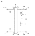
- FIG. 1 is a diagram showing a first example of a power conversion device according to the first embodiment.
- the power conversion device according to the first example includes external electrodes 1 to 4, noise filter 5, switching element 6, magnetic filter 7, first wiring 100, 101, and second wiring.
- the 103 and the third wirings 106 and 107 are provided.
- the first wiring 100 is connected between the external electrode 1 and the first input terminal 5a of the noise filter 5.
- the first wiring 101 is connected between the external electrode 2 and the second input terminal 5b of the noise filter 5.
- the third wiring 106 is connected between the first output terminal 5c of the noise filter 5 and the external electrode 3.
- the third wiring 107 is connected between the second output terminal 5d of the noise filter 5 and the external electrode 4.
- the first terminal of the magnetic filter 7 is connected to the third wiring 106.
- the second wiring 103 is connected between the second terminal of the magnetic filter 7 and the first terminal of the switching element 6.
- the second terminal of the switching element is connected to the third wiring 107. That is, the magnetic filter 7, the second wiring 103, and the switching element 6 are connected in series between the third wiring 106 and the third wiring 107 in this order.
- there is electrical continuity between the first wiring 100, the third wiring 106, and the second wiring 103 and there is electrical continuity between the first wiring 101 and the third wiring 107.
- the fact that there is electrical continuity means that the DC resistance is infinite, and in reality, the resistance value when measured with a tester or the like is smaller than at least 1 M ⁇ .
- A be the attenuation characteristic between the input and output of the noise filter 5.
- B the attenuation characteristic due to spatial propagation between the wirings.
- the attenuation characteristic of the filter is a characteristic proportional to the ratio of the power of the noise output from the filter to the power of the electromagnetic noise (hereinafter, also simply referred to as “noise”) input to the filter. say. That is, the fact that the noise filter 5 and the spatial propagation have a large attenuation characteristic means that the power of the output noise is smaller than the power of the input noise.
- the ratio of the power of the output noise to the power of the input noise is expressed using a logarithm because the output is a very small value such as 1/1000 with respect to the input 1. Specifically, if the power of the input noise is Win [W] and the power of the output noise is Wout [W], it is expressed as 10 ⁇ log 10 (Wout / Win).
- the first wirings 100 and 101, the second wiring 103, and the magnetic filter 7 are arranged so that the damping characteristic B is smaller than the damping characteristic A (B ⁇ A).
- the noise power is proportional to the square of the voltage or the square of the current
- the above relationship can be expressed by the voltage ratio or the current ratio. In this case, it can be expressed as 20 ⁇ log 10 (Vout / Vin).
- Vout / Vin the voltage ratio or the current ratio.
- the wavelength with respect to the frequency if the dimensions are about the same with respect to the wavelength, it is considered as a distribution constant. In such a distributed constant, the voltage and current values differ depending on the position of the measurement point. Therefore, it is generally desirable to consider the power (current ⁇ voltage) that is constant even in the distributed constant circuit.
- S-parameters also called scattering matrix, also called Scattering Parameter
- a network analyzer or a method applying the network analyzer for example, an impedance analyzer
- a method using an LCR meter or a TDR (Time Domain Reflectometry) method can also be used.
- FIG. 2 is a diagram showing a second example of the power conversion device according to the first embodiment.
- the power conversion device according to the second example is a power conversion device according to the first example shown in FIG. 1 with the reactor 8 added.
- the first terminal is connected to the third wiring 106, and the second terminal is connected to the first terminal of the second wiring 105.
- the second terminal of the second wiring 105 is connected to the first terminal of the magnetic filter 7.
- the first terminal of the second wiring 104 is connected between the second terminal of the magnetic filter 7 and the first terminal of the switching element 6.
- the second terminal of the switching element 6 is connected to the third wiring 107. That is, the reactor 8, the second wiring 105, the magnetic filter 7, the second wiring 104, and the switching element 6 are connected in series between the third wiring 106 and the third wiring 107 in this order.
- A be the attenuation characteristic of the noise filter 5.
- the attenuation characteristic due to spatial propagation between the wirings is defined as B. ..
- the first wirings 100 and 101, the second wiring 104, and the magnetic filter 7 are arranged so that the damping characteristic B is smaller than the damping characteristic A (B ⁇ A).
- the power conversion device has a circuit configuration of a single-phase two-wire input and a single-phase two-wire output.
- a power supply device such as a battery, a commercial power supply, or a solar panel, or a power conversion device such as an AC-DC converter described later may be connected to the external electrodes 1 and 2.
- Power is supplied to the external electrodes 1 and 2 by these devices.
- the external electrodes 3 and 4 are electrodes (terminals) that output the power generated by the power conversion device, and output DC power, AC power, or AC power on which DC power is superimposed.
- the current input to the external electrodes 1 and 2 is in the opposite direction from the external electrode 2 according to Kirchhoff's law. It is output with a current value equal to.
- a load such as a rotating machine or a battery, or a power conversion device such as a DC-DC converter or an AC-DC converter may be connected to the external electrodes 3 and 4.
- the external electrodes 1 and 2 are single-phase two-wire inputs
- the external electrodes 3 and 4 are single-phase two-wire outputs.
- the number of external electrodes should be changed for both the input and the output. It is also possible to correspond to general single-phase three-wire, three-phase three-wire, three-phase four-wire, and the like. In any configuration, the effect of the first embodiment can be obtained.
- the conduction noise is caused by noise (switching noise) generated at the moment when the switching element 6 is turned on or off.
- the noise includes the switching element 6 to the second wiring 104, the magnetic filter 7, the second wiring 105, the reactor 8, the third wiring 106, the noise filter 5, and the third wiring 107. 1 Return to the switching element 6 through the propagation path P1.
- the noise that cannot be completely removed by the noise filter 5 in the first propagation path P1 passes through the second propagation path P2.
- the second propagation path P2 flows from the switching element 6 to the external electrode 1 through the second wiring 104, the magnetic filter 7, the second wiring 105, the reactor 8, the third wiring 106, the noise filter 5, and the first wiring 100. This is a path that returns to the switching element 6 through the external electrode 2, the first wiring 101, the noise filter 5, and the third wiring 107.
- the third propagation path P3 flows from the switching element 6 through the second wiring 104, the magnetic filter 7, the second wiring 105, the reactor 8 and the third wiring 106 to the external electrode 3, and is connected to the external electrodes 3 and 4. This is a path that returns to the switching element 6 through the external electrode 4 and the third wiring 107 after passing through the load.
- the conduction noise propagates through the noise filter 5 and the wiring.
- the same can be considered for other power conversion devices.
- a semiconductor element is used for the switching element 6.
- semiconductor elements semiconductor elements used in power conversion devices are also referred to as "power semiconductor elements".
- Power semiconductor devices include those having a rectifying action such as a diode, those having an amplifying action such as an amplifier, and those having an action of conducting / blocking a current.
- the switching element 6 is a power semiconductor element having a rectifying action and a current conducting / blocking action.
- Si silicon
- wide bandgap semiconductors such as SiC (silicon carbide), GaN (gallium nitride), SiO (silicon oxide), and C (carbon) can be used as the material of the power semiconductor element.
- an IGBT Insulated Gate Bipolar Transistor
- MOSFET Metal Oxide Semiconductor Field Effect Transistor
- the switching element 6 (power semiconductor element) is mounted on a printed circuit board.
- the printed circuit board is on a dielectric formed of glass epoxy (FR-4: Flame Retardant Type 4) or paper phenol (FR-1,2), paper epoxy (FR-3), glass composite (CEM3), etc.
- FR-4 Flame Retardant Type 4
- FR-1,2 paper phenol
- FR-3 paper epoxy
- CEM3 glass composite
- a wiring made of a conductor such as copper or aluminum is formed.
- FR-4 is a glass fiber cloth impregnated with an epoxy resin and has a relative permittivity of about 4.
- a snubber circuit can also be used to reduce ringing and the like generated by the switching element 6. However, care must be taken because the power conversion efficiency decreases when a snubber circuit is used. Further, a heat dissipation mechanism such as a heat dissipation fin can be provided for heat dissipation of the switching element 6.
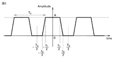
- FIG. 3 is a diagram schematically showing a time waveform of a voltage applied to the switching element 6.
- the switching element 6 is an IGBT
- a gate signal from a gate drive circuit not shown
- the switching element 6 is turned on, the collector-emitter voltage drops to 0%, and the collector-emitter current is generated. Flows.
- the gate signal is turned off, the switching element 6 is turned off, the current is cut off, and the collector-emitter voltage rises to 100%.
- the waveform shown in FIG. 3 can be created.
- the switching element 6 is a MOSFET, the current between the drain and the source is conducted or cut off according to the on / off of the gate signal input from the gate drive circuit.
- the switching element 6 When Si is used as the material of the power semiconductor element, the switching element 6 can be composed of an IGBT in order to obtain a dielectric strength. On the other hand, when a wide bandgap semiconductor is used as the material, the switching element 6 can be configured by a MOSFET that can be easily driven at high speed because the dielectric strength is high as a material characteristic.
- a power semiconductor element is called a switching element because it becomes a switch that conducts / cuts off current by turning on / off the gate signal. Then, by operating the switching element, magnetic energy is stored in the reactor (also referred to as coil, inductor or inductance) connected to the switching element, and the magnetic energy is discharged from the reactor to generate desired output power. can do.
- the reactor also referred to as coil, inductor or inductance
- the operating frequency of the switching element (hereinafter, also referred to as a drive frequency) is usually set to about 10 kHz to 100 kHz due to the relationship between heat generated by switching loss and heat dissipation.
- the drive frequency is usually set to about 30 kHz to 1 MHz.
- a high output voltage means a voltage of DC 300 V or more.
- the switching element is composed of a semiconductor, a bonding wire extending from the semiconductor, and a lead wire connected to the bonding wire, and the bonding wire and the lead wire are also of the second wiring. You can think of it as a part.
- the collector-emitter voltage drops from 500V to 0V within a time of about 30ns to 100ns at turn-on, and increases from 0V to 500V within a time of about 30ns to 100ns at turn-off.
- the switching element 6 is a MOSFET
- the drain-source voltage drops from 500V to 0V within a time of several ns to 30ns at turn-on, and 0V within a time of several ns to 30ns at turn-off. It rises from to 500V.
- the current shows a time change opposite to the time change of the voltage described above. Therefore, when the switching element 6 is turned on, the voltage drops to 0V and the current increases from 0A to several tens of A.
- the time waveforms of the voltage and current at this time have a trapezoidal wave shape as shown in FIG.
- one cycle T 0 of the voltage waveform corresponds to the reciprocal of the drive frequency of the switching element 6.
- the voltage rise time is set to the time from 0% to 100% (time from time-t2 / 2 to time-t1 / 2)
- the voltage fall time is set to 100% to 0%.
- the time time from time t1 / 2 to time t2 / 2 is defined, the definitions of rise time and fall time are not limited to this.
- ringing In the actual switching operation, ringing (overshoot and undershoot) occurs at the time of rising and falling, so the time waveform of voltage and current may not ideally be trapezoidal. Ringing is a high-frequency component (noise) superimposed on a trapezoidal wave, and depends exclusively on the design of the device such as the residual inductance of the wiring. Therefore, in this embodiment, ringing is ignored and the time waveforms of voltage and current are treated as ideal trapezoidal waves.
- FIG. 4 is a diagram schematically showing a frequency spectrum obtained by Fourier transforming the time waveform shown in FIG.
- the horizontal axis is the frequency and the vertical axis is the voltage, and both logarithms are taken.
- the Fourier transform shall be performed in a state where both ends of the time waveform are equal values (usually 0V or 0A). If both ends of the time waveform are not equal, a window function such as a humming window or hanning window is applied to the time waveform.
- the frequency spectrum shown in FIG. 4 has a constant amplitude in the frequency range of 0 [Hz] to 1 / ( ⁇ T 0) [Hz].
- the amplitude envelope decreases by -20 dB when the frequency increases 10 times (this is-). Also referred to as 20 dB / dec).
- the envelope of the amplitude is reduced by ⁇ 40 dB / dec.
- the time waveform of the voltage or current during the switching operation has a wide frequency component from a low frequency component to a high frequency component.
- frequency components of 1 / ( ⁇ T 0 ) [Hz] or higher correspond to noise and should be reduced.
- the rise time and fall time of the time waveform are different so as not to underestimate the noise, it is preferable to calculate the frequency component using the shorter time.
- the waveform after Fourier transform may be used for evaluation instead of the envelope.
- the wiring between the switching element 6 and the reactor 8 shall be designed so that the wiring pattern on the printed circuit board constituting the wiring and the wiring length of the cable are as short as possible. Is required.
- the reactor 8 is arranged close to the heat radiating plate or the heat radiating fin for heat dissipation, it is often actually arranged apart from the switching element 6 mounted on the printed circuit board. Further, since the reactor 8 is formed of a magnetic material such as an iron-based material and has a large weight, the reactor 8 may be arranged outside the printed circuit board in order to avoid deformation of the printed circuit board. In the present embodiment, it is considered that the reactor 8 is composed of a wiring portion wound around a magnetic material and a lead wire extending from the wiring portion, and the lead wire may also be considered as a part of the second wiring. ..
- the magnetic filter 7 can be mounted between the switching element 6 and the reactor 8.
- the wiring pattern forming the second wiring 104 between the switching element 6 and the magnetic filter 7 or the wiring length of the cable and the wiring routing are designed.
- the noise propagation characteristic (attenuation characteristic B) due to the magnetic coupling between the second wiring 104 and the first wirings 100 and 101 is lowered to be smaller than the attenuation characteristic A of the noise filter 5 (B ⁇ A). More preferably, the attenuation characteristic B is designed so that B [dB] + 6 dB ⁇ A [dB]. By setting the attenuation characteristic B with a margin of 6 dB or more in this way, it is significant between the attenuation characteristic A and the attenuation characteristic B in consideration of manufacturing errors or measurement errors such as routing of cables and wiring patterns. Can make a difference.
- the frequency characteristics of the magnetic filter 7 generally vary depending on the material.
- Mn—Zn-based ferrite, Ni—Zn-based ferrite, or the like is used depending on the drive frequency of the switching element 6.
- Mn—Zn-based ferrite can reduce noise of about 1 kHz to 1 MHz.
- Ni—Zn-based ferrite can reduce noise of about 1 MHz to 300 MHz.
- a normal mode choke coil, ferrite beads, or the like is mounted as the magnetic filter 7 on the second wiring 103 of the first example (see FIG. 1) and the second wirings 104 and 105 of the second example (see FIG. 2). Can be done.
- the magnetic filter 7 can be mounted in a non-contact manner by winding the cable in a state where the second wiring 104 and the second wiring 105 are connected like the ferrite core.
- the magnetic material may be magnetically saturated as the current capacity increases, a magnetic material filter 7 that does not magnetically saturate at the maximum rated current of the power converter is used.
- Magnetic saturation can be avoided by providing a gap (void) in the magnetic material or by using a magnetic material having a small relative magnetic permeability.
- magnetic saturation can be avoided by providing a heat dissipation mechanism in the magnetic material or by using a magnetic material having a large cross-sectional area.
- use a magnetic material such as the spike killer (amorphous magnetic material) manufactured by Toshiba Materials Co., Ltd., which is difficult to saturate, does not easily retain magnetic energy, and has a small back electromotive force (small noise) when the current is off. You can also.
- a gap may be formed in the magnetic filter 7.
- a cancel winding, a bifara winding, or the like can be used as the winding method when the wiring is attached to the magnetic filter 7.
- a split type ferrite core may be used so that the magnetic filter 7 can be retrofitted to the cable or the like.
- the impedance at the target frequency is large.
- the impedance of the magnetic filter 7 is given at 2 ⁇ fL (f is a frequency [Hz]), where L is the self-inductance of the magnetic filter 7.
- L is the self-inductance of the magnetic filter 7.
- the self-inductance of the cable is about 1 nH / mm, which is smaller than the self-inductance of the magnetic filter 7, the effect of the magnetic filter 7 can be obtained regardless of the inductance value of the magnetic filter 7.
- ⁇ Noise filter> At least one of a common mode choke coil, a normal mode choke coil, a line capacitor (also referred to as an X capacitor), a ground capacitor (also referred to as a Y capacitor), and a resistance element can be used for the noise filter 5. .. Since parts used for measures against dielectric lightning such as varistor or arrester have a capacitance component of about several 0.1 pF to several 100 pF, these parts can be used as a line capacitor or a ground capacitor.
- FIG. 5 is a diagram showing a first configuration example of the noise filter 5.
- the noise filter 5 according to the first configuration example includes input terminals 9, 10, output terminals 11, 12, line capacitors 13-1, 13-2, 13-3, and ground capacitors 14-1. , 14-2, 14-3, 14-4, 14-5, 14-6 and common mode choke coils 15-1, 15-2.
- the line capacitors 13-1, 13-2, and 13-3 are collectively referred to as the line capacitors 13.
- Ground-to-ground capacitors 14-1, 14-2, 14-3, 14-4, 14-5, 14-6 are also collectively referred to as ground-to-ground capacitors 14.
- the common mode choke coils 15-1 and 15-2 are collectively referred to as the common mode choke coil 15.
- the input terminal 9 is connected to the external electrode 1, and the input terminal 10 is connected to the external electrode 2.
- the output terminal 11 is connected to the external electrode 3, and the output terminal 12 is connected to the external electrode 4.
- the ground-to-ground capacitor 14 may be a reference potential in a housing or a printed circuit board that serves as a reference potential for the power conversion device, and does not necessarily have to be connected to the ground (ground, ground potential). Noise attenuation characteristics can be improved by arranging the ground-to-ground capacitors 14 in multiple stages. Further, by connecting two ground-to-ground capacitors 14 in series with respect to the line, it can also function as a part of the line capacitor.
- FIG. 6 is a diagram showing a second configuration example of the noise filter 5.
- the noise filter 5 according to the second configuration example includes input terminals 9, 10, output terminals 11, 12, line capacitors 13-1, 13-2, ground capacitors 14, and a common mode choke coil 15. It also has a normal mode choke coil 16.
- the normal mode choke coil may be magnetically saturated and the characteristics as a filter may be significantly deteriorated. Therefore, it is desirable to design the normal mode choke coil so that it does not magnetically saturate even when the maximum rated current flows.
- a noise filter such as a single-phase three-wire, three-phase three-wire, or three-phase four-wire can be similarly designed.
- the cable may be either a single wire or a stranded wire such as a litz wire. Copper, aluminum or iron, which have high conductivity, is generally used as the material of the cable, but an alloy of these or another material may be used.
- the wire diameter of the conducting wire may be any wire diameter that allows the maximum rated current to flow.
- the thickness and material of the covering member that covers the outer circumference of the conductor are not limited. However, considering that the dielectric breakdown withstand voltage of the conducting wire is about 1 kV / mm, it is necessary to prevent the dielectric breakdown withstand voltage of the covering member from becoming smaller than this.
- a connector such as a Faston terminal is attached to the tip of the cable by crimping, screwing, or soldering.
- a terminal block or bolts and nuts can be used.
- the contact resistance will increase and the cable or parts may be damaged by heat. Therefore, it is necessary to connect the cable and other parts so that the contact resistance becomes small.
- the contact force between parts is Ftc [N] and the contact resistance is Rtc [ ⁇ ]
- Rtc is proportional to 1 / ⁇ Ftc. That is, the contact resistance decreases as the contact force increases.
- ⁇ Load> Another power conversion device, a rotating machine (motor, compressor, etc.) or a secondary battery is connected as a load to the external electrodes 3 and 4 of the power conversion device according to the first embodiment.
- ICs that consume electric power to execute calculations, electric heaters such as heating wires, light sources, or sensors are connected to the external electrodes 3 and 4.
- Conduction noise generally refers to a high-frequency signal propagating via a cable such as a power supply line connected to the outside of an electronic device on which a power conversion device is mounted.
- Randomtion noise generally refers to a high frequency signal propagating to the outside of a device via space.
- Conduction noise is also referred to as noise terminal voltage, conduction emission, conduction EMI, conduction interference wave, interference power, noise power, and the like.
- Radiation noise is also referred to as radiation emission, radiation EMI, radiation jamming, jamming power, and the like.
- Embodiment 1 is also valid for other standards.
- Conduction noise is measured by measuring the output of a pseudo power network (also referred to as LISN or AMN) with a measuring instrument such as a spectrum analyzer or EMI receiver.
- a pseudo power network also referred to as LISN or AMN
- a measuring instrument such as a spectrum analyzer or EMI receiver.
- a receiving antenna is installed at a distance of 1 m to 10 m from the electronic device, and the electromagnetic wave output from the electronic device is received by the receiving antenna.
- the antenna end voltage is measured according to peak (PK: PEAK) detection, quasi-peak (QP: QUASI PEAK) detection, and average value (AV: AVERAGE) detection, and horizontal polarization or vertical polarization is measured. Further, in consideration of the directivity of the radio wave, the measurement is performed using a turntable or a device for measuring the height pattern.
- CISPR Comite International Special des Perturbations Radio /10, CISPR14, CISPR15, CISPR25, CISPR32, and IEC (International Electrotechnical Commission).
- IEC International Electrotechnical Commission
- the standard of conduction noise is defined in the range of 150 kHz to 30 MHz.
- the IEC further defines radiation noise standards in the range of 30 MHz to 1 GHz.
- High-frequency noise may interfere with the operation of electronic devices and may destroy the electronic circuits inside the electronic devices, so standards have been established to prevent these problems from occurring.
- the Electrical Appliance and Material Safety Law defines switching noise standards in the range of 500 kHz or higher
- CISPR defines switching noise standards in the range of 150 kHz or higher. According to the power conversion device according to the first embodiment, noise in these frequency ranges can be reduced.
- the power converter according to the first embodiment can construct the following four types of power converters by using a power semiconductor element for the switching element 6.
- the first power converter is a DC-AC converter (also called an inverter), which generates drive power for a motor or coil including a compressor.
- the second power converter is an AC-DC converter, which is used to charge a secondary battery or the like from a commercial power source.
- the third power converter is a DC-DC converter, which performs a step-up operation and / or a step-down operation so as to output a desired DC voltage.
- the fourth power converter is an AC-AC converter (also referred to as a matrix converter), which can generate an AC power source having a desired frequency.
- the power converter can be configured by combining a plurality of types of power converters. For example, by combining an AC-DC converter and a DC-AC converter, the power converter can generate an alternating current (AC) of any frequency from a commercial alternating current power supply (AC) to drive the rotating machine. Can be done. Further, by using the AC-DC converter, the boost DC-DC converter, and the DC-AC converter, a converter having high power conversion efficiency can be configured.
- AC alternating current
- AC commercial alternating current power supply
- a gate drive IC is generally used to control the on / off of the switching element included in the power converter.
- the gate drive IC is configured to control the gate voltage or gate current of the switching element.
- the above four types of power converters include those in which the input and output are not insulated and those in which the input and output are insulated. Unless otherwise specified in Embodiment 1, a non-insulated power converter shall be used. Even if an insulated power converter is used, the effect according to the first embodiment can be obtained.
- DC-DC converter Among DC-DC converters, those that are small and used as power supplies for electronic devices are also called switching regulators.
- the power conversion device according to the first embodiment can be applied to a switching regulator.
- the control of the switching regulator may be any of a current continuous mode, a current discontinuous mode, and a current critical mode.
- each of the step-up DC-DC converter, the step-down DC-DC converter, the step-up / down pressure DC-DC converter, and the four-quadrant chopper circuit will be described in order.
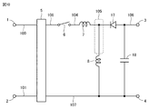
- FIG. 7 is a diagram showing a first configuration example of a boosted DC-DC converter to which the power conversion device according to the first embodiment is applied.
- the step-up DC-DC converter shown in FIG. 7 is obtained by adding a diode 17 and a smoothing capacitor 18 to the power conversion device (see FIG. 2) according to the second example.
- the diode 17 the anode is connected to the second wire 105 and the cathode is connected to the third wire 106.
- the smoothing capacitor 18 is connected between the third wiring 106 and the third wiring 107.
- the reactor 8 stores the energy of the DC power supply supplied via the external electrode 1 as magnetic energy in response to the turn-on of the switching element 6.
- the reactor 8 releases the stored magnetic energy. Since the emitted magnetic energy is superimposed on the output voltage of the DC power supply, the step-up DC-DC converter can output a voltage higher than the output voltage of the DC power supply.
- the smoothing capacitor 18 When the voltage is output, the voltage is also applied to both ends of the smoothing capacitor 18, so that electrical energy is stored in the smoothing capacitor 18. When the output voltage drops, the smoothing capacitor 18 releases the stored electrical energy. Thereby, the output voltage can be stabilized.
- the smoothing capacitor 18 a capacitor having a capacitance of about several hundred nF to several tens of mF can be used.
- the diode 17 is provided to prevent current from flowing from the smoothing capacitor 18 to the input side when the switching element 6 is in the off state. As a result, it is possible to suppress a decrease in the output voltage.
- the diode 17 is also referred to as a freewheeling diode.
- the magnetic filter 7 is connected in series with the switching element 6 via the second wiring 104.
- the magnetic filter 7 is connected to the reactor 8 and the diode 17 via the second wiring 105.
- the reactor 8 and the magnetic filter 7 and the diode 17 are used. Will be connected by a cable. Therefore, the magnetic filter 7 does not necessarily have to be mounted on the printed circuit board.
- the attenuation characteristic of the reactor 8 and the noise filter 5 combined can be regarded as the attenuation characteristic of the noise filter 5.
- a strong magnetic field is formed around the reactor 8, when the reactor 8 and the noise filter 5 are brought close to each other by several mm to several cm, the damping characteristics of the noise filter 5 alone and the noise filter 5 are used. It is necessary to compare the damping characteristics due to the spatial coupling including the magnetic coupling with the reactor 8.
- the attenuation amount in the latter attenuation characteristic cannot be significantly different from the attenuation amount of the noise filter 5 alone, it is necessary to provide a shield or the like.
- the wiring that constitutes the reactor 8 as a part of the second wiring 105, the wiring that constitutes the diode 17 as a part of the second wiring 105, and the wiring that constitutes the switching element 6 as a part of the second wiring 104 You may consider it.
- the reactor 8 since the reactor 8 is likely to be magnetically coupled to the magnetic material constituting the noise filter 5, the magnetic material filter and the like are designed according to the damping characteristics according to the present embodiment at the locations where the magnetic coupling is likely to occur as described above. There is a need to.
- FIG. 8 is a diagram showing a second configuration example of a step-up DC-DC converter to which the power conversion device according to the first embodiment is applied.
- the position of the magnetic filter 7 is different in the second configuration example shown in FIG. 8 as compared with the first configuration example shown in FIG. 7.
- the magnetic filter 7 is connected to the switching element 6 and the diode 17 via the second wiring 104.
- the total length of the second wiring 104 and the second wiring 104 connecting the switching element 6 and the reactor 8 is larger than the length of the second wiring 104 connecting the switching element 6 and the diode 17. It can be applied when it becomes long.
- a magnetic filter 7 such as a ferrite core is provided on the cable.
- the magnetic filter 7 having a large resistance component since the current flowing through the second wiring 104 is large, if the magnetic filter 7 having a large resistance component is used, the power conversion efficiency is lowered due to the heat generated by the magnetic filter 7.
- a magnetic filter 7 having a large inductance component is used in order to increase the impedance component while reducing the resistance component, the magnetic energy stored in the magnetic filter 7 becomes a voltage source at the moment when the switching element 6 is turned off. Become.
- back electromotive force is applied to both ends of the switching element 6, and a noise propagation path is formed due to the parasitic capacitance at both ends of the switching element 6, so that switching noise is likely to be generated. Therefore, it is desirable that the magnetic filter 7 has a small resistance component and is difficult to retain magnetic energy.
- FIG. 9 is a diagram showing a configuration example of a step-down DC-DC converter to which the power conversion device according to the first embodiment is applied.
- step-down DC-DC converter shown in FIG. 9, magnetic energy is stored in the reactor 8 when the switching element 6 is on, as in the step-down converter described above. At this time, due to the backflow prevention action of the diode 17 (reflux diode), a current flows only in the reactor 8. When the switching element 6 is turned off, the magnetic energy stored in the reactor 8 is released to the load. However, unlike the time of boosting, since the voltage and current on the power supply side are cut off by the switching element 6, it is possible to output the voltage stepped down to an arbitrary voltage according to the on-duty of the switching element 6.
- the attenuation characteristics of the noise filter 5 and the second wiring 104 and the first wiring 100 or 101 Compare with the damping characteristics due to the spatial coupling of. It is necessary that the damping characteristic of the space coupling is smaller than the damping characteristic of the noise filter 5.
- the attenuation characteristic due to spatial coupling can be made smaller than the attenuation characteristic of the noise filter 5. This makes it possible to enhance the apparent attenuation characteristic of the noise filter 5.
- FIG. 10 is a diagram showing a configuration example of a buck-boost converter to which the power conversion device according to the first embodiment is applied.
- the boost converter shown in FIG. 10 is similar to the boost converter shown in FIG. 7, but the power source is not connected between the external electrodes 1 and 2 when the magnetic energy stored in the reactor 8 is released. Different from boost converter. With such a configuration, the buck-boost converter can control the output voltage to 0 or more, and can be used for both the step-up circuit and the step-down circuit. However, it is necessary to use a reactor 8 having a large inductance value.
- the magnetic filter 7 is connected to the second wiring 104.
- the magnetic filter 7 is connected to the diode 17 and the reactor 8 via the second wiring 105.
- a ferrite core or the like may be attached to the cable.
- a magnetic filter 7 is provided.
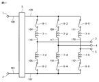
- FIG. 11 is a diagram showing a configuration example of a four-quadrant converter to which the power conversion device according to the first embodiment is applied.
- a four-quadrant converter is a circuit capable of outputting any combination of positive (output) and negative (input) DC output voltage and positive and negative output current.
- the four-quadrant converter shown in FIG. 11 controls the on / off of a plurality of switching elements to force and regenerate in the positive direction (the direction in which current flows from the external electrode 3 to the external electrode 4) and in the negative direction (external electrode). It is configured to be able to execute four types of operations of force running and regeneration (direction in which current flows from 4 to the direction of the external electrode 3).
- the four-quadrant converter has four switching elements 6-1 to 6-4, a reactor 8, four magnetic filter 7-1 to 7-4, and a noise filter 5. ..
- the four-quadrant converter has first wiring 100, 101, second wiring 104, 105, 109 to 112, and third wiring 106, 107.
- the magnetic filter 7-1 is connected to the switching element 6-1 via the second wiring 104, and is connected to the reactor 8 via the second wiring 111.
- the magnetic filter 7-2 is connected to the switching element 6-2 via the second wiring 105, and is connected to the reactor 8 via the second wiring 111.
- the magnetic filter 7-3 is connected to the switching element 6-3 via the second wiring 109, and is connected to the reactor 8 via the second wiring 112.
- the magnetic filter 7-4 is connected to the switching element 6-4 via the second wiring 110, and is connected to the reactor 8 via the second wiring 112.
- the attenuation characteristic due to spatial coupling can be made smaller than the attenuation characteristic of the noise filter 5, so that the attenuation characteristic of the noise filter 5 can be substantially enhanced.
- Such a configuration can be realized by routing the first wirings 100, 101 and the second wirings 104, 105, 109, 110 together with the positions where the magnetic filters 7-1 to 7-4 are connected. ..
- the wiring distance between the first wiring 100, 101 and any of the second wiring 104, 105, 109, 110 can be separated, the spatial coupling can be reduced, so that some switching elements can be used. Only the magnetic filter 7 can be provided.
- a magnetic filter 7-1 is attached between the second wirings 111 between the second wirings 104 and 105 and the reactor 8, and the second wirings 110 and 112 and the external electrode 4 are attached to each other.
- a magnetic filter 7-2 may be attached between them.
- the second wiring 106, 107 is connected to the magnetic filter 7-3,7-. 4 may be attached.
- FIG. 12 shows a configuration in which a magnetic filter is attached to each of the second wirings 106 and 107
- the second wirings 106 and 107 are wound around one magnetic component (for example, a ring-shaped core).
- a configuration that is, a configuration using a common mode filter may be used.
- the second wirings 110 and 112 may be wound around one magnetic component.
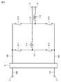
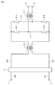
- FIG. 13 is a diagram showing a configuration example of a full bridge converter to which the power conversion device according to the first embodiment is applied.
- magnetic filters 7-1 to 7-4 are provided for each of the four switching elements 6-1 to 6-4, as in the case of the four-quadrant converter shown in FIG. Be done.
- the full bridge converter differs from the four quadrant converter in that it has a transformer 19, a smoothing capacitor 18, and a diode bridge 20.
- the transformer 19 is connected between the second wiring 111 and the second wiring 112. Since the primary winding of the transformer 19 can be regarded as a reactor, the power conversion device according to the first embodiment can be applied.
- a diode bridge 20 is connected to the secondary winding of the transformer 19. The voltage full-wave rectified by the diode bridge 20 is converted into a DC voltage by passing through the reactor 8 and the smoothing capacitor 18. By using a full bridge converter, a DC voltage of about several kV can be easily created.
- noise propagated by spatial coupling can be prevented by providing a magnetic filter between the switching element and the reactor in other isolated DC-DC converters such as flyback converters and forward converters. Can be reduced. As a result, it is possible to suppress a decrease in the attenuation characteristics of the noise filter 5.
- FIG. 14 is a diagram showing a first configuration example of an AC-DC converter to which the power conversion device according to the first embodiment is applied.
- the AC-DC converter has four switching elements 6-1 to 6-4.
- Four magnetic filter 7-1 to 7-4 are provided corresponding to the four switching elements 6-1 to 6-4.
- the magnetic filter 7-1 to 7-4 can reduce the noise propagated by the spatial coupling between the first wiring 100, 101 and the second wiring 104, 105, 109, 110.
- the spatial coupling can be efficiently reduced.
- the AC-DC converter may be composed of a diode bridge instead of a switching element.
- a diode bridge is not suitable for a switching circuit through which a large current flows because the loss due to the threshold voltage (resistance component) of the diode is large. Therefore, when a diode is used as a part of the switching element or when a switching element is used as a part of the diode bridge (for example, a totem pole type AC-DC converter), the power conversion device according to the first embodiment is applied. be able to.
- FIG. 15 is a diagram showing a step-up chopper composite rectifier circuit which is a second configuration example of an AC-DC converter to which the power conversion device according to the first embodiment is applied.
- the step-up chopper composite rectifier circuit performs full-wave rectification of the AC voltage by a diode bridge composed of four diodes 17-1 to 17-4, and then converts it into a DC voltage by the reactor 8. Further, the DC voltage is boosted by a booster circuit including a switching element 6, a diode 17, and a smoothing capacitor 18.
- the magnetic filter 7 between the switching element 6 and the reactor 8
- the spatial coupling between the second wiring 104 and the first wirings 100 and 101 can be reduced.
- the noise flowing between the external electrodes 1 and 2 can be reduced, so that the deterioration of the attenuation characteristics of the noise filter 5 can be suppressed.
- FIG. 16 is a diagram showing a first configuration example of a DC-AC converter to which the power conversion device according to the first embodiment is applied.
- FIG. 17 is a diagram showing a second configuration example of a DC-AC converter to which the power conversion device according to the first embodiment is applied.
- FIG. 16 is a configuration example in which the power conversion device according to the first embodiment is applied to the single-phase inverter
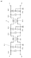
- FIG. 17 is a configuration example in which the power conversion device according to the first embodiment is applied to the three-phase inverter. Since there is no difference in the mounting method of the magnetic filter 7 between the single-phase inverter and the three-phase inverter, the first configuration example shown in FIG. 16 will be described below.
- the magnetic filter 7-1 to reduce the spatial coupling between each of the second wirings 104, 105, 109, 110 and the first wirings 100, 101. 7-4 is provided.
- the noise of the switching element 6-1 is propagated to the external electrode 3 through the second wiring 104 and returned from the external electrode 4 via the load connected between the external electrodes 3 and 4. Come on. Since the noise propagation path becomes long in this way, many spatial couplings are generated between the noise propagation paths and the first wirings 100 and 101. As a result, the attenuation characteristics when the noise filter 5 is connected to the switching elements 6-1 to 6-4 are deteriorated as compared with the attenuation characteristics of the noise filter 5 alone.
- the attenuation characteristics of the noise filter 5 are deteriorated by providing the magnetic filters 7-1 to 7-4 for the switching elements 6-1 to 6-4, respectively. It can be suppressed.
- the magnetic filters 7-1 to 7-4 having a large resistance component are used, the conversion efficiency is lowered. Further, when the magnetic materials filters 7-1 to 7-4 having a large inductance component are used, the magnetic energy stored in the magnetic material filters 7-1 to 7-4 becomes a voltage when the switching elements 6-1 to 6-4 are turned off. Become a source. As a result, a counter electromotive force is applied to both ends of the switching elements 6-1 to 6-4, and a noise propagation path is formed due to the parasitic capacitance at both ends of the switching elements 6-1 to 6-4. , It becomes easy to generate switching noise. Therefore, it is desirable that the magnetic filters 7-1 to 7-4 have a small resistance component and do not easily retain magnetic energy.
- the magnetic filter 7- is connected to the second wirings 111 and 112. It may be configured to attach 1 and 7-2 respectively. As a result, the number of magnetic filters can be reduced.
- the second wirings 111 and 112 may be wound around one magnetic filter 7-1. ..
- the spatial coupling in the present embodiment is satisfied between the switching elements 6-1 to 6-4 and the noise filter 5.
- the magnetic filter 7-2 may be provided.
- the magnetic filter 7-2 is described as a common mode filter through which the third wirings 106 and 107 are passed through one magnetic filter.
- the magnetic filter is divided into the first magnetic filter. It may be configured to be attached as a normal mode filter to each of the three wirings 106 and 107.
- AC-AC converter Although not shown, the power conversion device according to the first embodiment can be applied to the AC-AC converter.
- AC-AC converters include cycloconverters and matrix converters. Since a switching element is also used in these converters, by providing a magnetic filter in the vicinity of the switching element, spatial coupling can be reduced, and as a result, the attenuation characteristics of the noise filter 5 can be improved. ..
- the first embodiment shows a method of reducing the spatial propagation of noise caused by mutual inductance.
- the magnetic coupling in the present embodiment means mutual inductance.
- d indicates a minute amount
- dt indicates a minute time
- dI1 / dt indicates a change in current in a minute time. This change in current can be considered as a time change in noise current.
- FIG. 22 is a diagram illustrating the magnetic coupling between the two cables 26-1 and 26-2.
- the mutual inductance M due to the magnetic coupling of the cables 26-1 and 26-2 can be derived by the above equation (1).
- the cables 26-1 and 26-2 represent the first wiring 100, 101 and the second wiring 103, respectively, in the power conversion device according to the first embodiment.
- the mutual inductance M can be expressed by the following equation (3).
- the noise current flowing through one of the wirings When the time change dI / dt of the current (including the noise component) flowing through the wiring is not 0 in this way, the noise current flowing through one of the wirings generates a noise voltage in the conductor including the surrounding wirings.
- This noise voltage further forms a circuit via a conductor or space, and the impedance of the circuit generates a noise current.
- the second wiring 103 by reducing the magnetic field coupling between the second wiring 103 between the switching element 6 and the reactor 8 and the first wirings 100 and 101 between the external electrodes 1 and 2 and the noise filter 5 is reduced.
- the noise current flowing through the first wiring is prevented from being mixed into the first wiring.
- designing the positions of the noise filter 5 and the magnetic filter 7 and the wiring routing in consideration of the magnetic field coupling between the wirings is a concept not found in the prior art.
- the magnetic filter 7 is provided in the second wiring 103 connecting the switching element 6 and the reactor 8 so as to be close to the switching element 6. And. Further, the wirings of the second wiring 103 and the first wirings 100 and 101 connecting the external electrodes 1 and 2 and the noise filter 5 are separated from each other.
- the amount of noise propagation due to magnetic field coupling is reduced by increasing the distance between the wirings, but in the actual design, the attenuation characteristics of noise propagating in space due to magnetic field coupling are compared to the attenuation characteristics of the noise filter 5.
- the mutual inductance M is designed so that
- Parasitic capacitance also referred to as stray capacitance
- stray capacitance always occurs between two or more conductors. In this embodiment, two conductors are considered for simplicity.
- the parasitic capacitance C does not change unless the shape or dielectric constant of each conductor changes, or even if it changes, the amount of change is sufficiently smaller than dQ / dt and can be ignored. Therefore, C can be considered to be constant.
- the connector When a large voltage is applied between the two conductors due to the load, the effect of electric field coupling cannot be ignored. In a system where a large voltage is applied, the connector also becomes large. As a result, the distance between the switching element 6 or the reactor 8 and the connector may be short. In such a system, it is necessary to consider not only magnetic field coupling but also electric field coupling. As a countermeasure, the connector is arranged at a position separated by a spatial distance from the switching element 6 or the reactor 8. As a result, the amount of noise current mixed due to the electric field coupling between the connector and the switching element 6 or the reactor 8 is reduced.
- FIG. 23 is a diagram showing a configuration example of a power conversion device equipped with the noise filter 5 shown in FIG.
- the noise filter 5 is configured by combining a plurality of antistatic components such as an interline capacitor, an interground capacitor, a common mode choke coil, a normal mode choke coil, a diode, a resistor, and a varistor or an arrester.
- the ground-to-ground capacitor is attached to the housing of the power converter. If there is no housing, the ground-to-ground capacitor is installed at the reference potential.
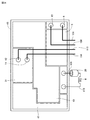
- FIG. 24 is a plan view showing a first example in which the power conversion device according to the first embodiment is mounted on a printed circuit board.
- a noise filter 5 a converter circuit 40, a reactor 8, an inverter circuit 31 and a control circuit 41 are mounted on the printed circuit board 43.
- a switching element 6 is mounted on the converter circuit 40.
- the reactor 8 and the printed circuit board 43 are connected by the second wiring 104.
- a ferrite core 30 is mounted on the second wiring 104 as a magnetic filter 7.
- the printed circuit board 43 is mounted with the first wirings 100 and 101 for connecting the external power supply to the external electrodes 9 and 10.
- the position of the ferrite core 30 and / or the routing of the first wiring 100, 101 and the second wiring 104 is designed.
- Third wirings 114 and 115 are connected to the output terminals 11 and 12 of the inverter circuit 31, respectively.
- a load (not shown) is connected to the third wirings 114 and 115.
- FIG. 25 is a diagram showing the measurement results of the noise terminal voltage in the power conversion device according to the first embodiment shown in FIGS. 23 and 24.
- the horizontal axis of FIG. 25 indicates the frequency, and the vertical axis indicates the noise terminal voltage.
- the test conditions are in accordance with CISPR14.
- a ferrite core 30 is used as the magnetic filter 7.
- the distance between each of the first wirings 100 and 101 and the second wiring 104 is widened from the initial value of 30 cm to 50 cm. Further, the distance between the ferrite core 30 and the switching element 6 of the converter circuit 40 is shortened from the initial value of 30 cm to 10 cm.
- a non-divided toroidal type ferrite is used for the ferrite core 30.
- the ferrite is wound twice around the second wiring 104 by bifara winding.
- the waveform 33 in FIG. 25 shows the measurement result of the noise terminal voltage of the power conversion device according to the first embodiment, and the waveform 34 shows the measurement result of the noise terminal voltage of the power conversion device in the initial state.
- Waveform 32 indicates a limit value of a standard defined by CISPR14.
- a GaN power semiconductor element is used for the switching element 6. Therefore, resonance occurs in the vicinity of 10 MHz due to the influence of the size of the housing, the inductance of the reactor 8, and the parasitic capacitance between the reactor 8 and the housing.
- the noise in the 10 MHz band has become more likely to occur.
- the noise propagating to the outside of the power conversion device without passing through the noise filter 5 is reduced by reducing the spatial coupling by installing the magnetic filter 7 and designing the distance between the wirings. Can be reduced.
- FIG. 26 is a plan view showing a second example in which the power conversion device according to the first embodiment is mounted on a printed circuit board.
- a noise filter 5 an inverter circuit 31, a converter circuit 40, a reactor 8, and a smoothing capacitor 18 are mounted on the printed circuit board 43.
- the first wirings 100 and 101 are connected between the external AC power supply and the noise filter 5.
- the electric power from the AC power supply is supplied to the inverter circuit 31 via the noise filter 5.
- the inverter circuit 31 converts AC power into DC power and outputs it.
- the converter circuit 40 converts this DC power into AC power of an arbitrary frequency and supplies it to the load via the third wirings 114 and 115.
- the reactor 8 and the smoothing capacitor 18 are mounted on a printed circuit board different from the printed circuit board 43 in consideration of their weight and heat generation.
- the converter circuit 40 is connected to the reactor 8 by the second wirings 104 and 119, and is also connected to the substrate on which the smoothing capacitor 18 is mounted by the wiring. Even in such wiring, it is possible to control the magnetic coupling by bringing the ferrite core 30 which is the magnetic filter 7 closer to the converter circuit 40.
- the noise filter 5 and the converter circuit 40 are mounted on the upper surface of the printed circuit board 43, and the reactor 8 and the smoothing capacitor 18 are arranged on the lower side of the printed circuit board 43. This is because warm air flows upward, so that the reactor 8 and the smoothing capacitor 18, which are sensitive to heat, are not heated, and the purpose is to reduce the inductance value of the reactor 8 due to heat or to extend the life of the smoothing capacitor. Therefore, it is difficult to arrange these parts apart from the first wirings 100 and 101.
- the first wirings 100 and 101 are usually connected via a terminal block, but the possibility of short-circuiting or corrosion increases when water droplets such as rain are applied, so the side close to the ground where direct rain is unlikely to be applied. Placed in. Therefore, it is difficult to arrange the first wirings 100 and 101 apart from the reactor 8 and the smoothing capacitor 18.
- the ferrite core 30 is attached to the second wiring 104 to remove the noise due to the magnetic coupling, thereby improving the apparent characteristics of the noise filter 5.
- the ferrite core 30 is attached only to the second wiring 104, but the second wiring 104 and the second wiring 119 may be wound around one ferrite core 30.
- the frequency is 100 MHz or less
- the effect of the ferrite core 30 can be enhanced by winding not only one turn but also a plurality of turns.
- the frequency is 100 MHz or more, by winding the wiring around the ferrite core 30 a plurality of times, the electric field coupling between the wound wirings increases, and the apparent characteristics of the ferrite core 30 are deteriorated. Therefore, it is desirable to set it to about 1 to 3 turns.
- Embodiment 2 In the second embodiment, normal mode noise and common mode noise will be described.
- Normal mode noise refers to noise in which a switching element, which is a noise source, is connected in series with a power supply line, and noise flows as a current in the same direction as the power supply current. Since the current flow and return are out of phase (phases differ by 180 degrees), it is also called normal mode or differential mode.
- Common mode noise is also called common mode because the currents flowing in the same direction with respect to the power supply line are in phase (phases match).
- the return of the common mode noise is the stray capacitance between the housing and the printed circuit board, the stray capacitance between the housing and the rotating machine, or the ground capacitor. It returns to the noise source via such as.
- FIG. 27 is a circuit diagram showing parts that affect the common mode component extracted from the noise filter 5 shown in FIG. Parts that do not affect the common mode component, such as line capacitors and normal mode choke coils, can be removed.
- FIG. 28 is a diagram showing the measurement results of the attenuation characteristics of the noise filter shown in FIG. 27 with respect to the common mode.
- the horizontal axis of FIG. 28 shows the frequency, and the vertical axis shows the attenuation characteristic.
- an attenuation characteristic for common mode noise of ⁇ 75 dB is obtained.
- a vector network analyzer or an impedance analyzer can be used to measure the noise filter.
- a vector network analyzer product name: E5061B, manufactured by Keysight was used.
- FIG. 29 is a diagram showing parts that affect the normal mode component extracted from the noise filter 5 of FIG.
- the line capacitor and the normal mode choke coil are effective in the normal mode, but in addition to that, the leakage inductance component of the common mode choke coil and the ground capacitor are series capacitors, so that they can be regarded as line capacitors.
- FIG. 30 is a diagram showing the measurement results of the attenuation characteristics of the noise filter shown in FIG. 29 with respect to the normal mode.
- the horizontal axis of FIG. 30 shows the frequency, and the vertical axis shows the attenuation characteristic.
- an attenuation characteristic for normal mode noise of ⁇ 82 dB is obtained.
- the first wiring 100 and the first wiring 101 are usually accompanied by each other within a few centimeters. This is because the first wirings 100 and 101 are often bundled and arranged in the device for ease of manufacturing, and the first wirings 100 and 100 are often fixed to the protrusions provided in the device. be.
- the normal mode noise is generated due to the difference in the wiring length of the cable or the difference in the impedance at both ends of the first wiring 100 and the first wiring 101 (for example, the impedance of the noise filter 5). Normal mode noise can also occur by changing from common mode noise to normal mode noise due to the phase shift of the first wiring 100 and the first wiring 101.
- the distance between the first wiring 100 and the second wiring 104 is different from the distance between the first wiring 101 and the second wiring 104, or when the orientation of the first wiring 100 and the second wiring 104 is the first.
- the normal mode noise increases.
- FIG. 31 is a diagram showing a result of comparing the mutual inductance M (Equation (3)) shown in the first embodiment with the characteristics of the noise filter shown in FIG. 28 with respect to the common mode component.
- the attenuation characteristic at the time of noise propagation due to magnetic coupling can be made smaller than that of the common mode component of the noise filter.
- the distance between the switching element 6 and the magnetic filter 7 is 1 cm, and the distance between the first wirings 100 and 101 and the second wiring 104 is 0.5 m.
- M ⁇ 0.01 nH can be obtained.
- the distance between the switching element 6 and the magnetic filter 7 is set to 1 cm or less, and the distance between the first wirings 100 and 101 and the second wiring 104 is set. Need to be separated by 0.5 m or more.
- the mutual inductance M is smaller than the M obtained from the equation (3) when the directions of the two wires are not parallel or when the two wires are in a twisting relationship.
- the angle formed by the directions of the two wirings is ⁇ with respect to the mutual inductance M0 at the closest distance between the two
- the mutual inductance M is calculated with M0 ⁇ cos ⁇ as an approximate value. Can be done.
- Embodiment 3 In the third embodiment, a design in consideration of the frequency characteristics of the noise filter 5 will be described.
- the noise filter 5 has frequency characteristics as shown in the measurement result of conduction noise shown in FIG. 25. Further, as shown in the first embodiment, the limit value determined by the noise standard (for example, the limit value 32 with respect to CISPR14 in FIG. 25) has a frequency characteristic.
- the mutual inductance between the first wiring and the second wiring shown in the first embodiment is obtained only for the frequency band exceeding the noise standard. Further, it is shown that the attenuation characteristic B due to the spatial coupling due to the parasitic capacitance is B ⁇ A with respect to the attenuation characteristic A of the noise filter 5.
- the noise in the frequency band of 7 to 10 MHz is strict with respect to the standard, and the noise filter 5 is designed so as to positively reduce the noise in the frequency band of 7 to 10 MHz. That is, only for such a frequency band, the noise attenuation characteristic B due to the spatial coupling between the first wirings 100 and 101 and the second wiring 103 is B ⁇ A rather than the attenuation characteristic A of the noise filter 5.
- the routing of the first wirings 100 and 101 and the second wiring 103 and the arrangement of the magnetic filter 7 are determined.
- the frequency characteristics of the switching element 6 that is the noise source the frequency characteristics of the noise propagation path, the frequency characteristics of the receiving port (LISN frequency characteristics in the case of conduction noise, and the frequency characteristics of the antenna itself in the case of radiation noise). ) Need to be grasped.
- the frequency characteristics of the switching element 6 that is a noise source can be estimated at the design stage as shown in FIGS. 3 and 4 of the first embodiment. Since the receiving port uses a fixed measuring instrument such as LISN, the frequency characteristics can be grasped.
- the issue is the frequency characteristics of the noise propagation path.
- Noise basically propagates along the propagation path of the circuit diagram, but it is necessary to consider other parasitic components.
- the impedance of the noise propagation path can be calculated by using equivalent circuit calculation software (product name: Q3D, manufactured by Ansys).
- Q3D equivalent circuit calculation software
- an electromagnetic field simulator for example, product name: HFSS, manufactured by Anysys, product name: MWstudio, CST, product name: FEMTET, manufactured by Murata Software, etc.
- Q3D electromagnetic field simulator
- a pseudo power supply network (AMN: Artificial Mains Network or LISN:), which is a measurement point, is used. It is possible to estimate the noise generated in (also called Line Impedance Stabilization Network).
- the self-inductance caused by the physical length of the wiring and the housing can be estimated from the theoretical formula without using a simulator. Specifically, regarding the calculation method, the self-inductance can be roughly calculated from Neumann's formula as well as the mutual inductance.
- Parasitic capacitance between wiring or IC on the housing and board, parasitic capacitance between housing and wiring, parasitic capacitance between housing and load, capacitance of the capacitor of noise filter 5, and capacitance of the measurement target as combined capacitance Can be calculated.
- the above-mentioned inductance component and capacitance component are combined and connected in series or in parallel when viewed from the switching element 6 which is a noise source.
- the noise propagation path has an impedance characteristic having resonances in a plurality of frequency bands. From the results, it is possible to reduce the noise mixed in the noise measurement location by making the amount of attenuation due to spatial coupling in these frequency bands smaller than the amount of attenuation of the noise filter 5. As a result, the resonance frequency can be predicted at the design stage, so that the frequency band to be reduced in the present embodiment can be grasped. As a result, wiring restrictions for reducing spatial coupling can be reduced, so that a smaller power conversion device can be provided at a lower cost.
- FIG. 32 is a perspective view showing an example of a power conversion device using the conductor plate 45 according to the fourth embodiment.
- a converter circuit 40 As shown in FIG. 32, a converter circuit 40, an inverter circuit 31, a control circuit 41, connectors 39-1, 39-2, 39-3, and a conductor plate 45 are mounted on the printed circuit board 43.
- the connector 39-1 connects the cable 38-1 connected to the commercial power supply 44 (not shown) and the printed circuit board 43.
- the cable 38-1 corresponds to the first wirings 100 and 101 shown in FIG.
- the noise filter 5 is connected to the connector 39-1, and the converter circuit 40 is connected to the noise filter 5.
- the inverter circuit 31 converts the DC power output from the converter circuit 40 into AC power.
- the control circuit 41 controls the converter circuit 40 and the inverter circuit 31.
- the connector 39-2 connects the cable 38-2 connected to the reactor 8 (not shown) mounted on the outside of the printed circuit board 43 and the converter circuit 40.
- the cable 38-2 corresponds to the second wiring 103 shown in FIG.
- the connector 39-3 connects the cable 38-3 connected to the load of the rotating machine or the like and the inverter circuit 31.
- the conductor plate 45 is connected to the ground on the printed circuit board 43 or a metal housing (not shown) around the printed circuit board 43.
- the conductor plate 45 may be connected to the ground on the printed circuit board 43 and may be connected to the metal housing by using another cable.
- the conductor plate 45 and the ground can be connected by soldering, screws, springs, bolts and nuts, crimping, connectors, or the like.
- the conductor plate 45 is not limited to one flat plate, and may be bent or may be composed of a plurality of plates. Further, the conductor plate 45 does not have to be mounted perpendicularly to the printed circuit board 43.
- the conductor plate 45 is provided at least in the second wiring 103 between the switching element 6 and the magnetic filter 7 including the ferrite core.
- the conductor plate 45 is provided on the second wiring 103 side connecting the switching element 6 and the magnetic filter 7, but on the first wiring 100, 101 side connecting the noise filter 5 and the external terminal.
- the conductor plate 45 may be connected to the.
- the thickness of the conductor plate 45 is not limited. It is desirable to cover the surface of the conductor plate 45 with a dielectric so that the conductor plate 45 does not short-circuit when it is unintentionally detached due to vibration or the like.
- the conductor plate 45 is mounted between the connectors 39-2, 39-3 and the converter circuit 40 and the inverter circuit 31, but the converter circuit 40 and the inverter circuit 31 and the noise filter 5 And the conductor plate 45 may be mounted between the control circuit 41 and the control circuit 41.
- the connector 39-1 and the connectors 39-2, 39-3 are attached diagonally on the printed circuit board 43 or at both ends of the long side of the printed circuit board 43.
- the distance between the cable 38-1 (corresponding to the first wirings 100 and 101 in FIG. 1) and the cable 38-2 (corresponding to the second wiring 103 in FIG. 1) can be increased, and the distance can be increased. It is possible to secure a space for arranging the conductor plate 45.
- FIG. 33 is a perspective view showing an example of a power conversion device using the magnetic shield 47 according to the fifth embodiment.
- a magnetic shield 47 made of a ferromagnetic material is used for the conductor plate 45 according to the fourth embodiment shown in FIG. 32.
- Ferromagnets include alloys containing iron, cobalt, nickel and the like.
- the magnetic shield 47 is placed on the ground on the printed circuit board 43 by utilizing the feature that the magnetic shield 47 sticks to the magnet.
- it may be attached to a metal housing (not shown).
- the magnetic shield 47 does not have to be electrically connected to the ground or the metal housing on the printed circuit board 43. That is, the magnetic shield 47 may be insulated from the ground and the metal housing (that is, it means that the DC resistance is sufficiently large).
- FIG. 34 is a diagram showing the measurement results of the shielding effect of paramagnetic materials (copper, aluminum, etc.) and ferromagnets.
- the paramagnetic material and the ferromagnetic material are insulated from the ground, and two loop probes, each of which has a diameter of 50 mm and is wound 10 times, are arranged with the loop surfaces facing each other at a distance of 5 mm. do. In this state, the spatial coupling between the two loop probes is measured.
- the damping characteristics were measured for each of the cases.
- the paramagnetic material is an aluminum plate having a thickness of 1 mm.
- the ferromagnet is an iron plate with a thickness of 1 mm.
- the waveform 48 shows (1) the damping characteristic when the conductor plate is not arranged
- the waveform 49 shows (2) the damping characteristic when the paramagnetic material is arranged
- the waveform 50 is (3) strong. The damping characteristics when a magnetic material is arranged are shown.
- the paramagnetic material can reduce the spatial coupling more than the ferromagnetic material in the frequency band lower than 10 MHz.
- noise of 1 MHz or less is often a problem for IGBTs and the like that are operated at low speeds.
- the space coupling between the wirings can be reduced by using a shield sheet metal made of a paramagnetic material.
- the magnetic shield 47 does not necessarily have to be connected to the ground, the possibility of a short circuit can be reduced even if the magnetic shield is unintentionally removed due to vibration or the like. Further, since the shield can be provided even for the power conversion device having no metal housing, the magnetic coupling can be reduced. Further, according to the magnetic shield 47, the degree of freedom of arrangement can be increased, and the steps of soldering or screw tightening can be reduced, so that the damping characteristics of the noise filter 5 can be improved at low cost.
- the mounting position of the magnetic shield 47 may be close to the second wiring 103 side or the first wiring 100, 101 side. No.
- Embodiment 6 In the sixth and seventh embodiments, an application example of the power conversion device shown in the fourth embodiment will be described.
- FIG. 35 is a diagram schematically showing a first configuration example of an air conditioner equipped with the power conversion device shown in FIG. 32.
- the outdoor unit 51 of the air conditioner has a fan 52, a partition plate 53, a compressor 54, and a printed circuit board 43.
- the space in which the fan 52 is arranged and the space in which the compressor 54 and the printed circuit board 43 are arranged are separated by a partition plate 53.
- the reactor 8 for the converter is attached to the conductor portion of the partition plate 53 for heat dissipation.
- the mounting position of the reactor 8 is not limited to this.
- the compressor 54 is arranged on the bottom surface of the outdoor unit 51.
- the compressor 54 is connected to the printed circuit board 43 via the cable 38-3.
- the printed circuit board 43 is connected to the reactor 8 via the cable 38-2.
- a ferrite core 30 is installed as a magnetic filter 7 on the cable 38-2.
- the ferrite core 30 is arranged close to the switching element 6 (not shown) on the printed circuit board 43.
- the cable 38-3 is arranged so as to be separated from the cable 38-2 in the depth direction in the drawing.
- the cable 38-1 is connected from the printed circuit board 43 to the commercial power supply 44 (not shown) of the outdoor unit 51.
- the outdoor unit 51 when measuring conduction noise, the outdoor unit 51 is connected to the LISN and then the outdoor unit 51 is connected to the commercial power source.
- the conductor plate 45 (or magnetic shield 47) is provided between the cable 38-2 and the cable 38-1, and between the cable 38-3 and the cable 38-1. As a result, the spatial coupling between the cable 38-2 and the cable 38-1 is reduced, and the spatial coupling between the cable 38-3 and the cable 38-1 is reduced.
- the noise attenuation characteristic of the noise filter 5 attached to the tip of the cable 38-1 when viewed from the commercial power supply 44 can be improved.
- the distance between the cable 38-1 and the cable 38-2 is 0.3 m or more.
- the distance between the wirings between the switching element 6 and the ferrite core 30 on the printed circuit board 43 is preferably 3 cm or less, and when there is a conductor plate 45 (or a magnetic shield 47), the distance between the wirings is 10 cm or less. Is desirable.
- FIG. 36 is a diagram schematically showing a second configuration example of the air conditioner equipped with the power conversion device shown in FIG. 32.
- the space where the fan 52 is arranged and the space where the printed circuit board 43 and the compressor 54 are arranged are arranged. Is separated from the partition plate 53.
- the reactor 8 is attached to the partition plate 53.
- the twisted cable 55-1 is used as the cable for connecting the printed circuit board 43 and the commercial power supply 44.
- a twisted cable 55-2 is used as a cable for connecting the switching element 6 (not shown) on the printed circuit board 43 and the reactor 8.
- the cable 38-3 that connects the inverter circuit (not shown) on the printed circuit board 43 and the compressor 54 does not have to be a twisted cable. This is because in a general outdoor unit 51, the inverter is often slower than the converter using the reactor 8.
- the printed circuit board 43 and each cable can be connected using a terminal block.
- the twisted cable may be used only for the cable arranged in the outdoor unit 51.
- the twisted pitch of the twisted cable is usually preferably about 10 mm to 50 mm.
- the switching element 6 is normally operating in the normal mode. Common mode occurs when the wiring or component through which normal mode current flows becomes an asymmetric propagation path. Therefore, the normal mode component is dominant as the noise component output by the switching element 6. According to this configuration example, the spatial propagation of the normal mode component of noise can be reduced by the twisted cable.
- Embodiment 8 In the eighth embodiment, the attachment position of the ferrite core 30 constituting the magnetic filter 7 to the cable will be described.
- FIG. 37 is a circuit diagram for explaining the mounting position of the ferrite core to the cable.
- the cable is marked with a mark indicating the mounting position of the ferrite core 30.
- a mark indicating the mounting position of the ferrite core 30 is provided on the cable.
- the cable is provided with a mark 56 indicating the start position at which the ferrite core 30 starts to be wound. Then, by winding two or more cables around the ferrite core 30, the ferrite core 30 is made difficult to move with respect to the cable.
- the mark 56 may be removed after the cable is wound by using a removable member such as a clip as the mark 56. Further, the shape of the mark 56 is not limited.
- the cable may be wound around the ferrite core 30 manually, or a machine such as a robot arm may be used.
- Embodiment 9 In the ninth embodiment, a method of fixing the ferrite core will be described with reference to FIG. 38.
- FIG. 38 is a diagram schematically showing a third configuration example of the air conditioner equipped with the power conversion device shown in FIG. 32.
- the outdoor unit of the air conditioner shown in FIG. 38 has the same basic configuration as the outdoor unit in the first configuration example of the air conditioner shown in FIG. 35.
- a ferrite core 30 having a weight of 5 to 200 g can be used as the ferrite core 30 attached to the outdoor unit.
- the ferrite core 30 may have a structure of hanging from the printed circuit board 43. In such a case, since a force is applied to the printed circuit board 43 or the connector on the printed circuit board 43, the components may be peeled off from the printed circuit board 43 or the cable may be disconnected from the printed circuit board 43.
- the ferrite core 30 is fixed.
- a hole is formed in the partition plate 53, and the ferrite core 30 is fixed to the partition plate 53 by using a fixing member 57 extending through the hole.
- the ferrite core 30 may be fixed to the printed circuit board 43 instead of the partition plate 53.
- the fixing member 57 is preferably a dielectric in order to prevent a short circuit or the like, but any material may be used. Further, in the examples of FIGS. 35, 36 and 38, the ferrite core 30 is hung from the printed circuit board 43, but in another air conditioner or power conversion device, the ferrite core is above the printed circuit board 43. It may be necessary to have a structure in which the 30s are arranged apart from each other. In that case, a structure in which the fixing member 57 is erected from the housing or the printed circuit board 43 to fix the ferrite core 30 can be adopted.
- FIG. 39 is a cross-sectional perspective view showing a configuration example of a cable according to the ninth embodiment.
- the cable according to the ninth embodiment has a shield structure for reducing noise in the normal mode.
- the cable when the power supply is a single-phase two-wire power supply, the cable has a structure in which the outer circumferences of the two core wires 58 are surrounded by an outer conductor 59 formed of a conductor.
- the core wire 58 is attached to the connector or terminal block described in the above embodiment.
- the first end of the outer conductor 59 is connected to the metal housing of the power conversion device, and the second end is connected to the ground on the printed circuit board.
- the ground on the printed circuit board has a reference potential and is usually conductive with the metal housing.
- the cable according to the ninth embodiment is applied to at least one of the first wirings 100 and 101 and the second wiring 103 in FIG. Thereby, it is possible to suppress the noise of the normal mode component and the common mode component from being transmitted and received via the spatial propagation.
- a shield structure can be provided for the twisted cables 55-1 and 55-2 by combining with the seventh embodiment shown in FIG.
- the ground (reference potential) which is the return path of the current is not a surface but a ground to which a Y capacitor is attached. It may be wiring.
- the outer conductor 59 of the cable will be connected to the ground wiring.
- This structure is generally called a pigtail structure and deteriorates the shield characteristics of the cable.
- the printed circuit board 43 is a multilayer board.
- FIG. 40 is a diagram showing the result of calculating the approximate value of the mutual inductance based on the parallel running distance of the two wirings and the distance between the wirings using the above equation (3).
- the horizontal axis of the graph of FIG. 40 shows the parallel running distance of the two wires, and the vertical axis shows the mutual inductance.
- the mutual inductance increases as the parallel running distance increases, regardless of the distance gap between the wirings.
- the mutual inductance decreases as the distance gap between the wirings increases.
- the noise attenuation characteristic is desired to be about -20 dB to -60 dB at 1 MHz.
- the above-mentioned design is performed for each of the normal mode and the common mode.
- the first wiring 100, 101 and the second wiring 103 shown in FIG. 1 are close to the same metal housing so that the two wirings do not run in parallel, the first wiring 100 and the metal housing are used. It is desirable that the distance between the wires 103 is 0.1 m or more and the distance between the second wiring 103 and the metal housing is 0.1 m or more.
- Embodiment 12 In the above-described embodiment, the method of reducing the conduction noise has been described, but according to the present embodiment, the radiation noise can also be reduced.
- the outside of the air conditioner is covered with a metal housing.
- the conductor plate 45 (or the magnetic shield 47) has a structure in which radiation noise is less likely to occur.
- the radiation noise standard is very small, such as 0 dB ⁇ V at 120 kHz. This standard corresponds to the electric power when the noise passing through the 120 kHz bandpass filter is measured by using the EMI receiver. Since the standard of radiation noise is very small, noise due to such secondary radiation can be a problem. Further, in air conditioners and other electronic devices, resin is often used as a part of a metal housing. Therefore, the shielding effect of the housing may not be obtained.
- FIG. 41 is a diagram showing a configuration example in which a power conversion device is arranged between the solar panel and the storage battery.
- a power conversion device in order to charge the power storage device such as a storage battery with the DC power generated by the solar panel 60, it is necessary to step up / down the voltage value of the DC power to an appropriate voltage value.
- DC-AC converter direct current power is converted to alternating current power by an inverter (DC-AC converter).
- the power conversion device according to the present embodiment can be applied to all the power devices having the power conversion device and the noise filter.
Landscapes
- Engineering & Computer Science (AREA)
- Power Engineering (AREA)
- Physics & Mathematics (AREA)
- Electromagnetism (AREA)
- Power Conversion In General (AREA)
- Inverter Devices (AREA)
Priority Applications (5)
| Application Number | Priority Date | Filing Date | Title |
|---|---|---|---|
| CN202080099821.9A CN115398786A (zh) | 2020-04-20 | 2020-04-20 | 电力变换装置以及空气调节机 |
| US17/913,871 US12009734B2 (en) | 2020-04-20 | 2020-04-20 | Power conversion device and air conditioner |
| EP20931798.1A EP4142134A4 (en) | 2020-04-20 | 2020-04-20 | POWER CONVERSION DEVICE AND AIR CONDITIONING |
| JP2020554913A JP6851554B1 (ja) | 2020-04-20 | 2020-04-20 | 電力変換装置および空気調和機 |
| PCT/JP2020/017057 WO2021214831A1 (ja) | 2020-04-20 | 2020-04-20 | 電力変換装置および空気調和機 |
Applications Claiming Priority (1)
| Application Number | Priority Date | Filing Date | Title |
|---|---|---|---|
| PCT/JP2020/017057 WO2021214831A1 (ja) | 2020-04-20 | 2020-04-20 | 電力変換装置および空気調和機 |
Publications (1)
| Publication Number | Publication Date |
|---|---|
| WO2021214831A1 true WO2021214831A1 (ja) | 2021-10-28 |
Family
ID=75154761
Family Applications (1)
| Application Number | Title | Priority Date | Filing Date |
|---|---|---|---|
| PCT/JP2020/017057 Ceased WO2021214831A1 (ja) | 2020-04-20 | 2020-04-20 | 電力変換装置および空気調和機 |
Country Status (5)
| Country | Link |
|---|---|
| US (1) | US12009734B2 (https=) |
| EP (1) | EP4142134A4 (https=) |
| JP (1) | JP6851554B1 (https=) |
| CN (1) | CN115398786A (https=) |
| WO (1) | WO2021214831A1 (https=) |
Cited By (2)
| Publication number | Priority date | Publication date | Assignee | Title |
|---|---|---|---|---|
| JP7531763B1 (ja) * | 2023-06-30 | 2024-08-09 | 三菱電機株式会社 | 電気機器 |
| WO2026038551A1 (ja) * | 2024-08-15 | 2026-02-19 | ニデック株式会社 | モータユニット |
Families Citing this family (5)
| Publication number | Priority date | Publication date | Assignee | Title |
|---|---|---|---|---|
| CN113258898B (zh) * | 2021-06-23 | 2025-06-10 | 珠海格力电器股份有限公司 | 一种滤波电路、滤波器及洗衣机 |
| WO2023013343A1 (ja) * | 2021-08-02 | 2023-02-09 | 株式会社村田製作所 | スイッチング電源装置 |
| JPWO2023079617A1 (https=) * | 2021-11-04 | 2023-05-11 | ||
| WO2024053006A1 (ja) * | 2022-09-07 | 2024-03-14 | 三菱電機株式会社 | 空気調和機の室外機 |
| JP7705061B2 (ja) * | 2023-09-29 | 2025-07-09 | ダイキン工業株式会社 | 電力変換装置、空気調和機 |
Citations (4)
| Publication number | Priority date | Publication date | Assignee | Title |
|---|---|---|---|---|
| JP2009060723A (ja) * | 2007-08-31 | 2009-03-19 | Fuji Electric Systems Co Ltd | 電力変換装置の制御装置および車両用静止形補助電源装置 |
| JP2009250521A (ja) | 2008-04-07 | 2009-10-29 | Panasonic Corp | 空気調和機の制御装置 |
| JP2013138552A (ja) * | 2011-12-28 | 2013-07-11 | Honda Motor Co Ltd | 負荷駆動装置 |
| JP2013150369A (ja) * | 2012-01-17 | 2013-08-01 | Mitsubishi Electric Corp | 系統連系用電力変換システム |
Family Cites Families (11)
| Publication number | Priority date | Publication date | Assignee | Title |
|---|---|---|---|---|
| JPS55164835U (https=) * | 1979-07-31 | 1980-11-27 | ||
| JP2003299386A (ja) | 2002-03-29 | 2003-10-17 | Mitsubishi Heavy Ind Ltd | 電動機用駆動制御装置 |
| EP2278694B1 (en) * | 2008-05-14 | 2017-06-28 | Daikin Industries, Ltd. | Filter circuit mounting unit and power source unit |
| JP5385939B2 (ja) * | 2011-04-21 | 2014-01-08 | 真 齋藤 | 電動機駆動システム |
| JP6176501B2 (ja) * | 2015-09-11 | 2017-08-09 | 株式会社安川電機 | 回路基板、及び電力変換装置 |
| JP6437959B2 (ja) * | 2016-06-30 | 2018-12-12 | トヨタ自動車株式会社 | 電力変換装置 |
| WO2019130874A1 (ja) * | 2017-12-27 | 2019-07-04 | 株式会社村田製作所 | 電源装置 |
| KR102524192B1 (ko) * | 2018-03-21 | 2023-04-21 | 현대자동차주식회사 | 전기 자동차의 충전 장치 |
| WO2020174563A1 (ja) * | 2019-02-26 | 2020-09-03 | 三菱電機株式会社 | 電気装置及び空気調和機 |
| JP7321377B2 (ja) * | 2020-07-13 | 2023-08-04 | 三菱電機株式会社 | ノイズフィルタ |
| JP7468275B2 (ja) * | 2020-09-29 | 2024-04-16 | 株式会社豊田自動織機 | ノイズフィルタ |
-
2020
- 2020-04-20 US US17/913,871 patent/US12009734B2/en active Active
- 2020-04-20 JP JP2020554913A patent/JP6851554B1/ja active Active
- 2020-04-20 WO PCT/JP2020/017057 patent/WO2021214831A1/ja not_active Ceased
- 2020-04-20 CN CN202080099821.9A patent/CN115398786A/zh not_active Withdrawn
- 2020-04-20 EP EP20931798.1A patent/EP4142134A4/en not_active Ceased
Patent Citations (4)
| Publication number | Priority date | Publication date | Assignee | Title |
|---|---|---|---|---|
| JP2009060723A (ja) * | 2007-08-31 | 2009-03-19 | Fuji Electric Systems Co Ltd | 電力変換装置の制御装置および車両用静止形補助電源装置 |
| JP2009250521A (ja) | 2008-04-07 | 2009-10-29 | Panasonic Corp | 空気調和機の制御装置 |
| JP2013138552A (ja) * | 2011-12-28 | 2013-07-11 | Honda Motor Co Ltd | 負荷駆動装置 |
| JP2013150369A (ja) * | 2012-01-17 | 2013-08-01 | Mitsubishi Electric Corp | 系統連系用電力変換システム |
Cited By (3)
| Publication number | Priority date | Publication date | Assignee | Title |
|---|---|---|---|---|
| JP7531763B1 (ja) * | 2023-06-30 | 2024-08-09 | 三菱電機株式会社 | 電気機器 |
| WO2025004347A1 (ja) * | 2023-06-30 | 2025-01-02 | 三菱電機株式会社 | 電気機器 |
| WO2026038551A1 (ja) * | 2024-08-15 | 2026-02-19 | ニデック株式会社 | モータユニット |
Also Published As
| Publication number | Publication date |
|---|---|
| EP4142134A1 (en) | 2023-03-01 |
| US12009734B2 (en) | 2024-06-11 |
| EP4142134A4 (en) | 2023-05-31 |
| CN115398786A (zh) | 2022-11-25 |
| JP6851554B1 (ja) | 2021-03-31 |
| JPWO2021214831A1 (https=) | 2021-10-28 |
| US20230344330A1 (en) | 2023-10-26 |
Similar Documents
| Publication | Publication Date | Title |
|---|---|---|
| JP6851554B1 (ja) | 電力変換装置および空気調和機 | |
| US10530193B2 (en) | Passive magnetic field attenuation | |
| Zhang et al. | Characteristics and influence factors of radiated disturbance induced by IGBT switching | |
| CN104270002B (zh) | Pwm功率变换器传导电磁干扰无源抑制方法 | |
| US11764613B2 (en) | Wireless power transfer pad with multiple windings and magnetic pathway between windings | |
| US9647535B2 (en) | Compact structure of power-supply apparatus capable of minimizing electromagnetic noise | |
| CN111490638A (zh) | 电控组件及电器设备 | |
| KR20190008385A (ko) | 전력 변환 장치 | |
| CN104518692B (zh) | 采集辐射性电磁干扰并利用其能量的切换式电源供应器 | |
| CN117849588B (zh) | 多电飞机系统传导电磁干扰交互作用的干扰源分析方法 | |
| JP2004319134A (ja) | 高周波加熱装置 | |
| US10559405B2 (en) | Cable configured to reduce a radiated electromagnetic field | |
| JP2022113013A (ja) | 電気機器 | |
| Sinclair et al. | A systematic study of EMI reduction by physical converter layout and suppressive circuits | |
| US12340939B2 (en) | Symmetric air-core planar transformer with partial electromagnetic interference shielding | |
| JP2020048404A (ja) | 電子電気機器 | |
| JP5338171B2 (ja) | スイッチング電源 | |
| CN208158433U (zh) | 铁路机车车载电子设备一次隔离电源模块 | |
| CN114629339A (zh) | 一种集成功率器件的电源模块电路及pcb板 | |
| US20150138058A1 (en) | Switched-Mode Power Supply Capable of Catching Radiated Electromagnetic Interference and Using its Energy | |
| WO2021257680A1 (en) | Isolated gate driver power supply device and related applications | |
| JP7672043B2 (ja) | 電力変換装置 | |
| CN207801779U (zh) | 一种基于lc谐振电路的脉冲电流发生器 | |
| CN117239947A (zh) | 一种提高功率输出的磁场能量收集装置 | |
| JP2010177100A (ja) | 高周波加熱装置用電源装置 |
Legal Events
| Date | Code | Title | Description |
|---|---|---|---|
| ENP | Entry into the national phase |
Ref document number: 2020554913 Country of ref document: JP Kind code of ref document: A |
|
| 121 | Ep: the epo has been informed by wipo that ep was designated in this application |
Ref document number: 20931798 Country of ref document: EP Kind code of ref document: A1 |
|
| NENP | Non-entry into the national phase |
Ref country code: DE |
|
| ENP | Entry into the national phase |
Ref document number: 2020931798 Country of ref document: EP Effective date: 20221121 |
|
| WWW | Wipo information: withdrawn in national office |
Ref document number: 2020931798 Country of ref document: EP |