WO2021210047A1 - 半導体素子の製造方法 - Google Patents
半導体素子の製造方法 Download PDFInfo
- Publication number
- WO2021210047A1 WO2021210047A1 PCT/JP2020/016312 JP2020016312W WO2021210047A1 WO 2021210047 A1 WO2021210047 A1 WO 2021210047A1 JP 2020016312 W JP2020016312 W JP 2020016312W WO 2021210047 A1 WO2021210047 A1 WO 2021210047A1
- Authority
- WO
- WIPO (PCT)
- Prior art keywords
- substrate
- circuit element
- semiconductor
- manufacturing
- support substrate
- Prior art date
- Legal status (The legal status is an assumption and is not a legal conclusion. Google has not performed a legal analysis and makes no representation as to the accuracy of the status listed.)
- Ceased
Links
Images


Classifications
-
- H—ELECTRICITY
- H10—SEMICONDUCTOR DEVICES; ELECTRIC SOLID-STATE DEVICES NOT OTHERWISE PROVIDED FOR
- H10P—GENERIC PROCESSES OR APPARATUS FOR THE MANUFACTURE OR TREATMENT OF DEVICES COVERED BY CLASS H10
- H10P10/00—Bonding of wafers, substrates or parts of devices
- H10P10/12—Bonding of semiconductor wafers or semiconductor substrates to semiconductor wafers or semiconductor substrates
-
- H—ELECTRICITY
- H10—SEMICONDUCTOR DEVICES; ELECTRIC SOLID-STATE DEVICES NOT OTHERWISE PROVIDED FOR
- H10D—INORGANIC ELECTRIC SEMICONDUCTOR DEVICES
- H10D30/00—Field-effect transistors [FET]
- H10D30/01—Manufacture or treatment
- H10D30/015—Manufacture or treatment of FETs having heterojunction interface channels or heterojunction gate electrodes, e.g. HEMT
-
- H—ELECTRICITY
- H10—SEMICONDUCTOR DEVICES; ELECTRIC SOLID-STATE DEVICES NOT OTHERWISE PROVIDED FOR
- H10D—INORGANIC ELECTRIC SEMICONDUCTOR DEVICES
- H10D62/00—Semiconductor bodies, or regions thereof, of devices having potential barriers
- H10D62/80—Semiconductor bodies, or regions thereof, of devices having potential barriers characterised by the materials
- H10D62/85—Semiconductor bodies, or regions thereof, of devices having potential barriers characterised by the materials being Group III-V materials, e.g. GaAs
- H10D62/8503—Nitride Group III-V materials, e.g. AlN or GaN
-
- H—ELECTRICITY
- H10—SEMICONDUCTOR DEVICES; ELECTRIC SOLID-STATE DEVICES NOT OTHERWISE PROVIDED FOR
- H10P—GENERIC PROCESSES OR APPARATUS FOR THE MANUFACTURE OR TREATMENT OF DEVICES COVERED BY CLASS H10
- H10P52/00—Grinding, lapping or polishing of wafers, substrates or parts of devices
-
- H—ELECTRICITY
- H10—SEMICONDUCTOR DEVICES; ELECTRIC SOLID-STATE DEVICES NOT OTHERWISE PROVIDED FOR
- H10P—GENERIC PROCESSES OR APPARATUS FOR THE MANUFACTURE OR TREATMENT OF DEVICES COVERED BY CLASS H10
- H10P54/00—Cutting or separating of wafers, substrates or parts of devices
-
- H—ELECTRICITY
- H10—SEMICONDUCTOR DEVICES; ELECTRIC SOLID-STATE DEVICES NOT OTHERWISE PROVIDED FOR
- H10P—GENERIC PROCESSES OR APPARATUS FOR THE MANUFACTURE OR TREATMENT OF DEVICES COVERED BY CLASS H10
- H10P72/00—Handling or holding of wafers, substrates or devices during manufacture or treatment thereof
- H10P72/70—Handling or holding of wafers, substrates or devices during manufacture or treatment thereof for supporting or gripping
- H10P72/74—Handling or holding of wafers, substrates or devices during manufacture or treatment thereof for supporting or gripping using temporarily an auxiliary support
- H10P72/7448—Handling or holding of wafers, substrates or devices during manufacture or treatment thereof for supporting or gripping using temporarily an auxiliary support the bond interface between the auxiliary support and the wafer comprising two or more, e.g. multilayer adhesive or adhesive and release layer
- H10P72/745—Handling or holding of wafers, substrates or devices during manufacture or treatment thereof for supporting or gripping using temporarily an auxiliary support the bond interface between the auxiliary support and the wafer comprising two or more, e.g. multilayer adhesive or adhesive and release layer the bond interface between the auxiliary support and the wafer comprises three or more layers
-
- H—ELECTRICITY
- H10—SEMICONDUCTOR DEVICES; ELECTRIC SOLID-STATE DEVICES NOT OTHERWISE PROVIDED FOR
- H10P—GENERIC PROCESSES OR APPARATUS FOR THE MANUFACTURE OR TREATMENT OF DEVICES COVERED BY CLASS H10
- H10P72/00—Handling or holding of wafers, substrates or devices during manufacture or treatment thereof
- H10P72/70—Handling or holding of wafers, substrates or devices during manufacture or treatment thereof for supporting or gripping
- H10P72/74—Handling or holding of wafers, substrates or devices during manufacture or treatment thereof for supporting or gripping using temporarily an auxiliary support
- H10P72/7412—Handling or holding of wafers, substrates or devices during manufacture or treatment thereof for supporting or gripping using temporarily an auxiliary support the auxiliary support including means facilitating the separation of a device or wafer from the auxiliary support
-
- H—ELECTRICITY
- H10—SEMICONDUCTOR DEVICES; ELECTRIC SOLID-STATE DEVICES NOT OTHERWISE PROVIDED FOR
- H10P—GENERIC PROCESSES OR APPARATUS FOR THE MANUFACTURE OR TREATMENT OF DEVICES COVERED BY CLASS H10
- H10P72/00—Handling or holding of wafers, substrates or devices during manufacture or treatment thereof
- H10P72/70—Handling or holding of wafers, substrates or devices during manufacture or treatment thereof for supporting or gripping
- H10P72/74—Handling or holding of wafers, substrates or devices during manufacture or treatment thereof for supporting or gripping using temporarily an auxiliary support
- H10P72/7416—Handling or holding of wafers, substrates or devices during manufacture or treatment thereof for supporting or gripping using temporarily an auxiliary support used during dicing or grinding
-
- H—ELECTRICITY
- H10—SEMICONDUCTOR DEVICES; ELECTRIC SOLID-STATE DEVICES NOT OTHERWISE PROVIDED FOR
- H10P—GENERIC PROCESSES OR APPARATUS FOR THE MANUFACTURE OR TREATMENT OF DEVICES COVERED BY CLASS H10
- H10P72/00—Handling or holding of wafers, substrates or devices during manufacture or treatment thereof
- H10P72/70—Handling or holding of wafers, substrates or devices during manufacture or treatment thereof for supporting or gripping
- H10P72/74—Handling or holding of wafers, substrates or devices during manufacture or treatment thereof for supporting or gripping using temporarily an auxiliary support
- H10P72/7422—Handling or holding of wafers, substrates or devices during manufacture or treatment thereof for supporting or gripping using temporarily an auxiliary support used to protect an active side of a device or wafer
-
- H—ELECTRICITY
- H10—SEMICONDUCTOR DEVICES; ELECTRIC SOLID-STATE DEVICES NOT OTHERWISE PROVIDED FOR
- H10P—GENERIC PROCESSES OR APPARATUS FOR THE MANUFACTURE OR TREATMENT OF DEVICES COVERED BY CLASS H10
- H10P72/00—Handling or holding of wafers, substrates or devices during manufacture or treatment thereof
- H10P72/70—Handling or holding of wafers, substrates or devices during manufacture or treatment thereof for supporting or gripping
- H10P72/74—Handling or holding of wafers, substrates or devices during manufacture or treatment thereof for supporting or gripping using temporarily an auxiliary support
- H10P72/744—Details of chemical or physical process used for separating the auxiliary support from a device or a wafer
Definitions
- This disclosure relates to a method for manufacturing a semiconductor device.
- the thickness of a semiconductor element has been reduced in order to package the semiconductor element at a high density to reduce the size of the semiconductor module, or to join a heat-dissipating substrate to the semiconductor element to improve the performance (hereinafter, "thinning"). Also called) is required.
- the thinning of the semiconductor element is performed by the following process. First, the circuit element surface of the semiconductor element is adhered to the support substrate, and the opposite surface is mechanically and chemically polished. Next, the support substrate is peeled off from the semiconductor element. In these steps, it is necessary to prevent cracks or breakage in the thinned semiconductor element.
- Patent Document 1 describes a method in which a semiconductor substrate having a thickness of 1130 ⁇ m is adhered to a support substrate with electron wax, the back surface of the semiconductor substrate is polished, a transfer substrate is bonded to the back surface of the semiconductor substrate, and the support substrate is peeled off by heating. It is shown.
- Patent Document 2 discloses a method of removing a substrate by etching instead of polishing. Specifically, an organic insulating film is applied onto the semiconductor layer on the Si substrate except for the end portion of the wafer formed by the Si substrate and the semiconductor layer. Next, an inorganic insulating film is formed so as to cover the organic insulating film. After that, the surfaces of the wafer and the support substrate are activated in vacuum, and the wafer is bonded to the support substrate. After that, the Si substrate is removed by etching.
- Patent Document 3 describes a method for manufacturing a semiconductor element having a chip-on-chip structure.
- the semiconductor wafer includes a Si substrate and an element layer on the Si substrate. Through electrodes straddling both the Si substrate and the element layer are formed. After the insulating film and the metal layer are sequentially formed on the element layer, the metal layer of the semiconductor wafer is bonded to the metal layer of the support substrate. The back surface of the wafer is polished until the through silicon vias are exposed from the back surface, and then the supporting substrate is removed by polishing and etching.
- the present disclosure has been made to solve the above problems, and an object of the present disclosure is to provide a method for manufacturing a thin semiconductor device having a low defect rate.
- a circuit element substrate including a semiconductor substrate and a circuit element on the semiconductor substrate is prepared, an electrode protection layer is formed on the circuit element, a support substrate is prepared, and a circuit is performed in vacuum.
- a metal thin film is formed on the electrode protection layer of the element substrate and the support substrate, and the metal thin films of the circuit element substrate and the support substrate are bonded to each other by the atomic diffusion bonding method to bond the circuit element substrate and the support substrate.
- the semiconductor substrate is polished and removed to expose the circuit element, the transfer substrate is bonded to the exposed surface of the circuit element, and the support substrate is peeled off from the circuit element after the transfer substrate is bonded.
- FIG. It is a flowchart which shows the manufacturing method of the semiconductor element of Embodiment 1. It is sectional drawing which shows the manufacturing method of the semiconductor element of Embodiment 1. It is sectional drawing which shows the manufacturing method of the semiconductor element of Embodiment 1. It is sectional drawing which shows the manufacturing method of the semiconductor element of Embodiment 1. It is sectional drawing which shows the manufacturing method of the semiconductor element of Embodiment 1. It is sectional drawing which shows the manufacturing method of the semiconductor element of Embodiment 1. It is sectional drawing which shows the manufacturing method of the semiconductor element of Embodiment 1. It is sectional drawing which shows the manufacturing method of the semiconductor element of Embodiment 1. It is sectional drawing which shows the manufacturing method of the semiconductor element of Embodiment 1. It is sectional drawing which shows the manufacturing method of the semiconductor element of Embodiment 1.
- FIG. 1 is a cross-sectional view showing the configuration of the semiconductor element 101 of the first embodiment.
- the semiconductor element 101 includes a circuit element 2 and a transfer substrate 10.
- the transfer board 10 is joined to the lower surface of the circuit element 2.
- the circuit element 2 is a HEMT (high electron mobility transistor) having gallium nitride (GaN) as a semiconductor layer, but is a MOSFET (metal-oxide-semiconductor field-effect transistor) or an IGBT (insulated gate bipolar transistor). ) And other circuit elements may be used.
- the thickness of the circuit element 2 is, for example, 10 ⁇ m.
- the transfer substrate 10 is a substrate having high thermal conductivity, for example, a diamond substrate.
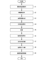
- FIG. 2 is a flowchart showing a manufacturing method of the semiconductor element 101. Hereinafter, a method of manufacturing the semiconductor element 101 will be described according to the flow of FIG.
- the circuit element substrate 7 includes a semiconductor substrate 1 and a circuit element 2 formed on the semiconductor substrate 1.
- the semiconductor substrate 1 is, for example, a Si wafer, a SiC (silicon carbide) wafer, or the like.
- the circuit element 2 includes a hollow bridge electrode connecting the electrodes, and although not shown in FIG. 3, there is a step due to the electrodes on the upper surface of the circuit element 2. It is necessary to form a protective layer on the circuit element 2 in order to prevent damage to the electrodes in the subsequent polishing step. Therefore, as shown in FIG. 4, the electrode protection layer 3 is coated and formed on the circuit element 2 (step S1). The electrode protection layer 3 not only protects the electrodes of the circuit element 2 in the subsequent polishing step, but also has the effect of increasing the bonding strength with the support substrate by flattening the irregularities of the electrodes.
- an adhesive composed of an organic solvent and a thermosetting resin or a photocurable resin, or a photoresist material, which can be removed by chemical treatment or oxygen ashing in the final step is selected.
- an acrylic resin, an olefin resin, a phenol resin, a polypropylene resin, a polyethylene resin, a polyethylene resin or the like is used for the electrode protective layer 3.
- a material having a high substrate strength in which the circuit element substrate 7 and the support substrate are integrated and which does not cause peeling or cracking in the polishing process is effective. From that viewpoint, an acrylic resin is effective.
- a material having high film strength such as epoxy resin is preferable.
- the electrode protective layer 3 For coating the electrode protection layer 3, for example, a spin coating method is used in which an adhesive is dropped on the main surface of the circuit element substrate 7 on which the circuit element 2 is formed, and the circuit element substrate 7 is rotated at high speed. However, other coating methods such as printing or spraying may be used.
- the electrode protective layer 3 has a thickness of 5 ⁇ m or more and 8 ⁇ m or less, and is formed so as to cover the circuit element 2. After applying the electrode protective layer 3 on the circuit element 2, the electrode protective layer 3 is cured.
- a thermosetting resin is used as the material of the electrode protective layer 3
- the solvent component evaporates and cures when the electrode protective layer 3 is heated to 90 ° C. or higher and 120 ° C. or lower by a hot plate or the like.
- a photocurable resin is used as the material of the electrode protective layer 3, the electrode protective layer 3 is cured by irradiating the circuit element substrate 7 with light.
- a release layer 5 is formed on the adhesive surface of the transparent substrate 4 to prepare the support substrate 8 (step S2). That is, the support substrate 8 includes a transparent substrate 4 and a release layer 5 formed on the transparent substrate 4.
- the transparent substrate 4 has light transmittance and is made of non-alkali glass, sapphire glass, or the like.
- the release layer 5 made of a photodegradable material that decomposes when it absorbs light such as laser or infrared rays is formed on the transparent substrate 4.
- a peeling layer 5 is formed by applying a paste composed of a resin containing a carbon material that absorbs light, generates heat, and thermally decomposes to a transparent substrate 4 by a spin coating method, and heat-drying the paste. ..
- a carbon film having a thickness of 1 ⁇ m or more and 2 ⁇ m or less may be formed as the release layer 5 on the transparent substrate 4 by a CVD sputtering device. When the carbon film is used for the release layer 5, the support substrate 8 can be firmly adhered to the circuit element substrate 7.
- the surface of the release layer 5 is mirror-finished by lapping polishing.
- the arithmetic mean roughness of the surface of the release layer 5 is preferably less than 0.5 nm, more preferably less than 0.2 nm. If the arithmetic mean roughness of the surface of the peeling layer 5 is less than 0.5 nm, it is possible to reduce the portion that is not adhered to the circuit element substrate 7 in the subsequent process, and the adhesive strength to the circuit element substrate 7 is increased.
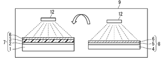
- the circuit element substrate 7 and the support substrate 8 are set in the vacuum chamber 9 and exhausted to an ultra-high vacuum of 10-6 Pa.
- a metal thin film 6 is formed on the electrode protection layer 3 of the circuit element substrate 7 and the release layer 5 of the support substrate 8 by a sputtering method or a vapor deposition method to a thickness of several nm or more and several tens of nm or less.
- FIG. 6 shows how sputter atoms are emitted from the sputtering target 12 onto the electrode protection layer 3.
- the material of the metal thin film 6 aluminum, copper, silicon, titanium, gold, silver, iron, chromium and the like are used.
- step S4 the metal thin films 6 are bonded to each other in the vacuum chamber 9 to join the circuit element substrate 7 and the support substrate 8 (step S4).
- step S3 The formation of the metal thin film 6 (step S3) and the joining of the circuit element substrate 7 and the support substrate 8 (step S4) are continuously performed in the same vacuum chamber 9. If the circuit element substrate 7 and the support substrate 8 are taken out into the atmosphere after the metal thin film 6 is formed, moisture, a natural oxide film or an organic substance adheres to the surface, and the metal thin films 6 do not bond to each other. Therefore, in order to bond the circuit element substrate 7 and the support substrate 8, it is necessary to irradiate the circuit element substrate 7 and the support substrate 8 with an ion beam or a neutral atom beam again in a vacuum to clean the circuit element substrate 7.
- step S3 and step S4 since the atomic diffusion bonding method is used in which the metal thin films 6 are formed on the circuit element substrate 7 and the support substrate 8 in a vacuum and then the metal thin films 6 are bonded to each other in the same vacuum, an atomic beam or the like is used. No need for surface activation by. Therefore, there is no loss in the process, and the process time of the joining step (step S3 and step S4) can be shortened from 10 minutes to 15 minutes. Therefore, if a cassette that can set several wafers at a time is used and a load lock chamber, which is a preliminary exhaust chamber, is provided in the vacuum chamber 9, it is compared with the process of attaching a substrate using a general adhesive. The processing time can be shortened.
- the thickness of the resin film is as thick as several hundred ⁇ m or more and several mm, and the elastic modulus of the resin film is small. .. Therefore, the substrate strength after bonding is low, and when the circuit element substrate 7 is polished to be thinned, cracks occur in the peripheral portion of the circuit element substrate 7 or the circuit element substrate 7 is peeled off from the support substrate 8. Problems occur.
- the thickness of the adhesive layer can be made very thin, from about 0.2 nm to 20 nm for one atom.
- the adhesive force is strong and the mechanical strength of the bonded substrate is high. Therefore, defects such as cracks, peeling or breakage during polishing or dicing are reduced.
- the substrate is not thermally expanded and distorted by heating. Therefore, the material of the substrate to be joined is not selected.
- the surface of the bonding substrate composed of the circuit element substrate 7 and the support substrate 8 on the circuit element substrate 7 side is polished to remove the semiconductor substrate 1 (step S5).
- the reason for removing the semiconductor substrate 1 is to improve the heat dissipation efficiency of the circuit element 2 and to obtain low power consumption and high output.
- the semiconductor substrate 1 having a thickness of 500 ⁇ m is polished to a thickness of 20 ⁇ m.
- the polishing method mechanical polishing, chemical polishing, chemical mechanical polishing, or the like is used.
- the remaining semiconductor substrate 1 having a thickness of 20 ⁇ m is removed by dry etching such as reactive ion etching (RIE).
- RIE reactive ion etching
- the semiconductor substrate 1 is completely removed, and the lower surface of the circuit element 2 is exposed. Then, chemical mechanical polishing is performed to obtain the flatness of the lower surface of the circuit element 2. It is desirable that the arithmetic average roughness Ra of the lower surface of the circuit element 2 is 0.5 nm or less in consideration of the bonding with the transfer substrate 10 to be performed later.
- the strength of the circuit element substrate 7 including the circuit element 2 decreases. Therefore, the circuit element 2 is deformed due to the influence of the stress of the residual film, and cracks or peeling occur in the peripheral portion of the circuit element 2 due to uneven polishing.
- the semiconductor substrate 1 is polished in a state where the circuit element substrate 7 is firmly adhered to the support substrate 8, the strength of the circuit element substrate 7 is maintained even if the semiconductor substrate 1 is removed. Therefore, defects such as deformation, cracking, and peeling of the circuit element 2 are suppressed.
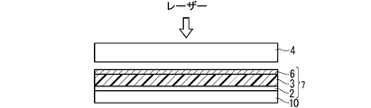
- the lower surface of the circuit element 2 is joined to the transfer substrate 10 (step S6).
- the transfer substrate 10 for example, a diamond substrate having excellent thermal conductivity is used.
- the transfer substrate 10 has a thickness of 100 ⁇ m, and the arithmetic average roughness of the joint surface is 0.5 nm or less by precision polishing.
- the same atomic diffusion bonding method as the bonding of the support substrate 8 described above is used.
- the coefficient of thermal expansion of diamond constituting the transfer substrate 10 is 2.3 ⁇ 10 -6 / K, which is significantly different from the coefficient of thermal expansion of gallium nitride constituting the circuit element 2 of 5.5 ⁇ 10 -6 / K. ..
- the circuit element 2 and the transfer substrate 10 may be bonded by irradiating the bonding surface with a neutral atom beam to remove the natural oxide film or the organic substance, and then using a surface activation method of bonding.
- the arithmetic average roughness of the joint surface between the circuit element 2 and the transfer substrate 10 is set to 0.5 nm or less by surface polishing.
- the support substrate 8 is peeled off from the circuit element substrate 7 (step S7). Specifically, the support substrate 8 is peeled off by irradiating a laser from the upper surface of the transparent substrate 4 to heat and decompose the peeling layer 5.
- the number of steps is small, the processing time is short, and the transparent substrate 4 can be reused, so that the productivity is improved and the productivity is improved. Production cost can be reduced.
- step S8 dicing is performed as shown in FIGS. 10 and 11, and the bonding substrate including the transfer substrate 10 and the circuit element substrate 7 is divided into a plurality of chips (step S8).
- FIG. 11 shows one chip after division. Many elements are formed in the circuit element 2, and each element is divided in this step.
- the dicing method laser dicing, plasma dicing or the like can be used. Conventionally, cracks, peeling, or chipping have occurred in the circuit element substrate 7 in the dicing process due to the decrease in strength due to the thinning.
- the circuit element substrate 7 is directly bonded to the support substrate 8 to increase the strength, the above-mentioned problems are suppressed.
- step S9 the metal thin film 6 and the electrode protective layer 3 are peeled off from the individualized chip.
- the circuit element substrate 7 is immersed in an alkaline or acidic stripping solution, an organic solvent, or the like, and the metal thin film 6 and the electrode protective layer 3 are dissolved and removed. Then, the residual organic matter is washed and the circuit element substrate 7 is dried.
- the metal thin film 6 may be removed with an acidic stripping solution, and the electrode protective layer 3 may be removed with oxygen ashing. In this way, the semiconductor element 101 shown in FIG. 1 is completed.
- a circuit element substrate 7 including the semiconductor substrate 1 and the circuit element 2 on the semiconductor substrate 1 is prepared, and an electrode is provided on the circuit element 2.
- a protective layer 3 is formed, a support substrate 8 is prepared, a metal thin film 6 is formed on the electrode protective layer 3 and the support substrate 8 of the circuit element substrate 7 in vacuum, and the circuit element substrate 7 and the support substrate 8 are formed.
- the substrates 10 are joined, and after the transfer substrate 10 is joined, the support substrate 8 is peeled off from the circuit element 2. Since the metal thin films 6 of the circuit element substrate 7 and the support substrate 8 are firmly bonded to each other by the atomic diffusion bonding method, the mechanical strength of the bonded substrate to which the circuit element substrate 7 and the support substrate 8 are bonded is increased. Therefore, even if the semiconductor substrate 1 is polished to make the semiconductor element thinner, defects such as cracks, peeling, or breakage are less likely to occur in the circuit element 2, and the defect rate can be lowered.
- FIG. 12 is a cross-sectional view of the semiconductor element 102 of the second embodiment.
- the semiconductor element 102 includes a circuit element 2, an inorganic insulating film 11 formed on the upper surface of the circuit element 2, and a transfer substrate 10 formed on the lower surface of the circuit element 2.
- the circuit element 2 and the transfer substrate 10 are as described in the first embodiment.
- the inorganic insulating film 11 is an electrode protective layer.
- the resin was used for the electrode protective layer 3 of the first embodiment, the inorganic insulating film having high thermal conductivity is used as the electrode protective layer in the second embodiment, so that this is referred to as the inorganic insulating film 11. Refer to.
- the strength of the bonding substrate between the circuit element substrate 7 and the support substrate 8 is improved as compared with the case where a resin is used, and cracks or peeling of the semiconductor substrate 1 after polishing are suppressed. be able to.
- the inorganic insulating film 11 is not removed and is used as a heat radiating material on the upper surface side of the circuit element 2, thereby improving the heat radiating performance of the semiconductor element 102 and omitting the step of removing the inorganic insulating film 11.
- the inorganic insulating film 11 is an inorganic insulating film having high thermal conductivity.
- FIG. 13 shows a semiconductor substrate 1 and a circuit element substrate 7 including a circuit element 2 on the semiconductor substrate 1. Since the circuit element 2 has a hollow bridge electrode connecting the electrodes, a step is formed on the upper surface of the circuit element 2 as shown in FIG. The height of this step is about several ⁇ m.
- the circuit element substrate 7 is put into a film forming apparatus such as a CVD plasma apparatus, and as shown in FIG. 14, an inorganic insulating film 11 having high thermal conductivity is formed on the circuit element 2 to be equal to or higher than the height of the electrode in the circuit element 2. It is formed with the thickness of.
- a film forming apparatus such as a CVD plasma apparatus
- an inorganic insulating film 11 having high thermal conductivity is formed on the circuit element 2 to be equal to or higher than the height of the electrode in the circuit element 2. It is formed with the thickness of.
- the material of the inorganic insulating film 11 diamond, aluminum nitride, silicon nitride, beryllium oxide or the like can be used.
- the electrode protective layer can be used as a heat sink on the upper surface side of the circuit element 2, so that the step of removing the electrode protective layer becomes unnecessary. Therefore, it is possible to shorten the process time and improve the device performance.
- the electrode protective layer 3 of the first embodiment is a resin
- the resin flows by using the spin coating method, and the upper surface of the electrode protective layer 3 is formed flat.
- the inorganic insulating film 11 is formed by a CVD method or the like, a step is formed on the upper surface of the inorganic insulating film 11 as shown in FIG.
- the high portion of the inorganic insulating film 11 is flattened to the same height as the electrodes of the circuit element 2 by a polishing method.
- the arithmetic mean roughness of the upper surface of the inorganic insulating film 11 at this time is 1.0 nm or less.
- Step S3 After cleaning the upper surface of the inorganic insulating film 11 to remove polishing residues, the formation of the metal thin film 6 (step S3), the circuit element substrate 7 (step S4), and the support substrate 8 are performed in the same manner as in the first embodiment.
- Step S5 polishing the semiconductor substrate 1 (step S6), joining the transfer substrate 10 (step S7), peeling the support substrate 8 (step S8), and dividing the circuit element 2 (step S9).
- the metal thin film 6 is removed from the upper surface of the inorganic insulating film 11, and the semiconductor element 102 shown in FIG. 12 is completed.
- the inorganic insulating film 11 remains on the upper surface of the circuit element 2 and functions as a heat sink.
- the electrode protective layer formed on the upper surface of the circuit element 2 is an inorganic insulating film 11 made of an inorganic insulating material. Therefore, as compared with the case where resin is used for the electrode protection layer, the strength of the bonding substrate between the circuit element substrate 7 and the support substrate 8 is improved, and cracks or peeling of the semiconductor substrate 1 after polishing can be suppressed.
- the inorganic insulating film 11 is an inorganic insulating film having high thermal conductivity, the inorganic insulating film 11 can be used not only as an electrode protective layer but also as a heat radiating material on the upper surface side of the circuit element 2. Therefore, the heat dissipation of the semiconductor element 102 can be improved, and the step of removing the electrode protective layer can be omitted.
Landscapes
- Mechanical Treatment Of Semiconductor (AREA)
Priority Applications (6)
| Application Number | Priority Date | Filing Date | Title |
|---|---|---|---|
| CN202080099340.8A CN115428127B (zh) | 2020-04-13 | 2020-04-13 | 半导体元件的制造方法 |
| PCT/JP2020/016312 WO2021210047A1 (ja) | 2020-04-13 | 2020-04-13 | 半導体素子の製造方法 |
| KR1020227032511A KR102718211B1 (ko) | 2020-04-13 | 2020-04-13 | 반도체 소자의 제조 방법 |
| JP2022514883A JP7186921B2 (ja) | 2020-04-13 | 2020-04-13 | 半導体素子の製造方法 |
| EP20931548.0A EP4138116B1 (en) | 2020-04-13 | 2020-04-13 | Method for manufacturing semiconductor element |
| US17/912,053 US12387934B2 (en) | 2020-04-13 | 2020-04-13 | Method of manufacturing semiconductor element |
Applications Claiming Priority (1)
| Application Number | Priority Date | Filing Date | Title |
|---|---|---|---|
| PCT/JP2020/016312 WO2021210047A1 (ja) | 2020-04-13 | 2020-04-13 | 半導体素子の製造方法 |
Publications (1)
| Publication Number | Publication Date |
|---|---|
| WO2021210047A1 true WO2021210047A1 (ja) | 2021-10-21 |
Family
ID=78084736
Family Applications (1)
| Application Number | Title | Priority Date | Filing Date |
|---|---|---|---|
| PCT/JP2020/016312 Ceased WO2021210047A1 (ja) | 2020-04-13 | 2020-04-13 | 半導体素子の製造方法 |
Country Status (6)
| Country | Link |
|---|---|
| US (1) | US12387934B2 (https=) |
| EP (1) | EP4138116B1 (https=) |
| JP (1) | JP7186921B2 (https=) |
| KR (1) | KR102718211B1 (https=) |
| CN (1) | CN115428127B (https=) |
| WO (1) | WO2021210047A1 (https=) |
Families Citing this family (2)
| Publication number | Priority date | Publication date | Assignee | Title |
|---|---|---|---|---|
| US12347717B2 (en) * | 2021-06-24 | 2025-07-01 | Taiwan Semiconductor Manufacturing Company, Ltd. | Debonding structures for wafer bonding |
| JP2025020566A (ja) * | 2023-07-31 | 2025-02-13 | 株式会社東芝 | 半導体装置の製造方法 |
Citations (5)
| Publication number | Priority date | Publication date | Assignee | Title |
|---|---|---|---|---|
| JPH1174230A (ja) * | 1997-08-29 | 1999-03-16 | Nippon Telegr & Teleph Corp <Ntt> | 薄膜半導体装置の製造方法 |
| JP2005129825A (ja) | 2003-10-27 | 2005-05-19 | Sumitomo Chemical Co Ltd | 化合物半導体基板の製造方法 |
| JP2007188967A (ja) * | 2006-01-11 | 2007-07-26 | Sony Corp | 基板支持体、基板処理方法及び半導体装置の製造方法 |
| JP2007324406A (ja) | 2006-06-01 | 2007-12-13 | Sony Corp | 基板処理方法及び半導体装置の製造方法 |
| JP2012028477A (ja) | 2010-07-22 | 2012-02-09 | Sumitomo Electric Ind Ltd | 半導体装置の製造方法 |
Family Cites Families (10)
| Publication number | Priority date | Publication date | Assignee | Title |
|---|---|---|---|---|
| JPH11261198A (ja) * | 1998-03-11 | 1999-09-24 | Dainippon Printing Co Ltd | 転写用原版を用いた配線基板の製造方法と転写用原版、および該転写用原版の製造方法 |
| US6593213B2 (en) * | 2001-09-20 | 2003-07-15 | Heliovolt Corporation | Synthesis of layers, coatings or films using electrostatic fields |
| JP2004055593A (ja) * | 2002-07-16 | 2004-02-19 | Hoya Corp | 配線基板およびその製造方法 |
| US20140144593A1 (en) * | 2012-11-28 | 2014-05-29 | International Business Machiness Corporation | Wafer debonding using long-wavelength infrared radiation ablation |
| JP6299478B2 (ja) * | 2013-06-26 | 2018-03-28 | 日亜化学工業株式会社 | 発光装置およびその製造方法 |
| JP6210152B2 (ja) * | 2014-04-10 | 2017-10-11 | 富士電機株式会社 | 半導体基板の処理方法及び該処理方法を用いる半導体装置の製造方法 |
| WO2018216763A1 (ja) | 2017-05-25 | 2018-11-29 | 株式会社新川 | 構造体の製造方法及び構造体 |
| KR102558905B1 (ko) | 2017-07-14 | 2023-07-21 | 신에쓰 가가꾸 고교 가부시끼가이샤 | 고열전도성의 디바이스 기판 및 그 제조 방법 |
| JP7041338B2 (ja) * | 2017-09-01 | 2022-03-24 | 日亜化学工業株式会社 | 発光装置の製造方法 |
| JP7002398B2 (ja) * | 2018-04-13 | 2022-01-20 | 株式会社ディスコ | 光学部品の接合方法 |
-
2020
- 2020-04-13 EP EP20931548.0A patent/EP4138116B1/en active Active
- 2020-04-13 JP JP2022514883A patent/JP7186921B2/ja active Active
- 2020-04-13 WO PCT/JP2020/016312 patent/WO2021210047A1/ja not_active Ceased
- 2020-04-13 US US17/912,053 patent/US12387934B2/en active Active
- 2020-04-13 KR KR1020227032511A patent/KR102718211B1/ko active Active
- 2020-04-13 CN CN202080099340.8A patent/CN115428127B/zh active Active
Patent Citations (5)
| Publication number | Priority date | Publication date | Assignee | Title |
|---|---|---|---|---|
| JPH1174230A (ja) * | 1997-08-29 | 1999-03-16 | Nippon Telegr & Teleph Corp <Ntt> | 薄膜半導体装置の製造方法 |
| JP2005129825A (ja) | 2003-10-27 | 2005-05-19 | Sumitomo Chemical Co Ltd | 化合物半導体基板の製造方法 |
| JP2007188967A (ja) * | 2006-01-11 | 2007-07-26 | Sony Corp | 基板支持体、基板処理方法及び半導体装置の製造方法 |
| JP2007324406A (ja) | 2006-06-01 | 2007-12-13 | Sony Corp | 基板処理方法及び半導体装置の製造方法 |
| JP2012028477A (ja) | 2010-07-22 | 2012-02-09 | Sumitomo Electric Ind Ltd | 半導体装置の製造方法 |
Non-Patent Citations (1)
| Title |
|---|
| See also references of EP4138116A4 |
Also Published As
| Publication number | Publication date |
|---|---|
| US20230134255A1 (en) | 2023-05-04 |
| EP4138116B1 (en) | 2024-03-13 |
| US12387934B2 (en) | 2025-08-12 |
| EP4138116A1 (en) | 2023-02-22 |
| KR102718211B1 (ko) | 2024-10-15 |
| JP7186921B2 (ja) | 2022-12-09 |
| CN115428127A (zh) | 2022-12-02 |
| JPWO2021210047A1 (https=) | 2021-10-21 |
| CN115428127B (zh) | 2025-02-18 |
| KR20220143741A (ko) | 2022-10-25 |
| EP4138116A4 (en) | 2023-07-19 |
Similar Documents
| Publication | Publication Date | Title |
|---|---|---|
| TWI749087B (zh) | 將裝置層轉印至轉印基板之方法及高導熱性基板 | |
| CN113454758B (zh) | 半导体元件的制造方法 | |
| TWI798236B (zh) | 高熱傳導性之元件基板及其製造方法 | |
| JP3502036B2 (ja) | 半導体素子の製造方法および半導体素子 | |
| CN105960707B (zh) | 装卸器晶片移除 | |
| CN116856051A (zh) | 降低外延层破碎几率的金刚石基氮化镓晶圆的制备方法 | |
| JP7186921B2 (ja) | 半導体素子の製造方法 | |
| CN113013061B (zh) | 一种利用有机薄膜进行化合物半导体加工的方法 | |
| WO2020235074A1 (ja) | 半導体基板の製造方法および半導体装置の製造方法 | |
| JP6775722B1 (ja) | 研磨方法、半導体基板の製造方法 | |
| CN116978786A (zh) | 金刚石基氮化镓晶体管制备方法及金刚石基氮化镓晶体管 | |
| JP2005129653A (ja) | 半導体装置の製造方法 | |
| TWI845377B (zh) | 半導體製造方法 | |
| CN118645450A (zh) | 碳化硅晶圆的返工处理方法及半导体器件 | |
| CN118315287A (zh) | 一种芯片的制造方法 | |
| JP7182105B2 (ja) | Iii族窒化物半導体デバイスの製造方法 | |
| WO2022168217A1 (ja) | 半導体基板の製造方法および半導体装置の製造方法 | |
| CN120690699A (zh) | 一种薄片晶圆的加工方法和半导体制品 | |
| CN110783178A (zh) | 一种半导体晶片及其加工方法 |
Legal Events
| Date | Code | Title | Description |
|---|---|---|---|
| 121 | Ep: the epo has been informed by wipo that ep was designated in this application |
Ref document number: 20931548 Country of ref document: EP Kind code of ref document: A1 |
|
| ENP | Entry into the national phase |
Ref document number: 2022514883 Country of ref document: JP Kind code of ref document: A |
|
| ENP | Entry into the national phase |
Ref document number: 20227032511 Country of ref document: KR Kind code of ref document: A |
|
| NENP | Non-entry into the national phase |
Ref country code: DE |
|
| ENP | Entry into the national phase |
Ref document number: 2020931548 Country of ref document: EP Effective date: 20221114 |
|
| WWG | Wipo information: grant in national office |
Ref document number: 202080099340.8 Country of ref document: CN |
|
| WWG | Wipo information: grant in national office |
Ref document number: 17912053 Country of ref document: US |